Embed Size (px)
Citation preview
1
Numerical study of the thermoelectric power factor
in ultra-thin Si nanowires
Neophytos Neophytou and Hans Kosina
Institute for Microelectronics, TU Wien, Gußhausstraße 27-29/E360, A-1040 Wien, Austria
e-mail: {neophytou|kosina}@iue.tuwien.ac.at
Abstract
Low dimensional structures have demonstrated improved thermoelectric (TE)
performance because of a drastic reduction in their thermal conductivity, κl. This has
been observed for a variety of materials, even for traditionally poor thermoelectrics such
as silicon. Other than the reduction in κl, further improvements in the TE figure of merit
ZT could potentially originate from the thermoelectric power factor. In this work, we
couple the ballistic (Landauer) and diffusive linearized Boltzmann electron transport
theory to the atomistic sp3d
5s*-spin-orbit-coupled tight-binding (TB) electronic structure
model. We calculate the room temperature electrical conductivity, Seebeck coefficient,
and power factor of narrow 1D Si nanowires (NWs). We describe the numerical
formulation of coupling TB to those transport formalisms, the approximations involved,
and explain the differences in the conclusions obtained from each model. We investigate
the effects of cross section size, transport orientation and confinement orientation, and the
influence of the different scattering mechanisms. We show that such methodology can
provide robust results for structures including thousands of atoms in the simulation
domain and extending to length scales beyond 10nm, and point towards insightful design
directions using the length scale and geometry as a design degree of freedom. We find
that the effect of low dimensionality on the thermoelectric power factor of Si NWs can be
observed at diameters below ~7nm, and that quantum confinement and different transport
orientations offer the possibility for power factor optimization.
Index terms: thermoelectrics, tight-binding, atomistic, sp3d
5s*, Boltzmann transport,
Seebeck coefficient, thermoelectric power factor, silicon, nanowire, ZT.
2
I. Introduction
The ability of a material to convert heat into electricity is measured by the
dimensionless figure of merit ZT=σS2T/(κe+κl), where σ is the electrical conductivity, S is
the Seebeck coefficient, and κe and κl are the electronic and lattice part of the thermal
conductivity, respectively. The interrelation between σ, S, and κe in bulk materials keeps
ZT low [1]. Some of the best thermoelectric materials are compounds of Bi, Te, Pb, Sb,
Ag, and exhibit ZT ~ 1 [1, 2]. Recently, however, using low-dimensional structures, it
was demonstrated that ZT could be greatly increased compared to their bulk counterparts,
setting the stage for highly efficient TE energy conversion.
It was initially suggested that thermoelectric efficiency could be improved at the
nanoscale because of two reasons: i) Low-dimensionality and quantum size effects could
improve the Seebeck coefficient [3], and ii) Small feature sizes enhance phonon
scattering on nanoscale interfaces and reduce thermal conductivity [4]. Indeed, large
improvements of ZT in low-dimensional structures such as 0D quantum dots, 1D
nanowires (NWs), 2D superlattices and bulk nanocomposites have recently been
achieved [4, 5, 6, 7, 8, 9, 10, 11, 12, 13, 14]. This was even achieved for common
materials, and importantly Si based systems such as Si, SiGe, and SiC [15, 12, 13, 14].
Silicon, the most common semiconductor with the most advanced industrial processes, is
a poor TE material with ZTbulk~0.01. Si NWs, on the other hand, have demonstrated
ZT~1, a 100X increase [12, 13, 14, 15], and they are now considered as emerging
candidates for high efficiency and large volume production TE applications [16].
Most of the benefit to the measured ZT values of NWs originates from a dramatic
reduction in the lattice thermal conductivity κl [15, 17, 18, 19, 20]. It has very recently
become evident, however, that benefits from κl reduction are reaching their limits, and
further increases of ZT can only be achieved through improvements in the power factor
σS2 [16, 21]. By nanostructuring, the electronic structure could be engineered to tune the
Seebeck coefficient [3, 7, 22] and the electrical conductivity [23] independently, which
could maximize σS2. For example, Hicks and Dresselhaus suggested that the sharp
3
features in the low-dimensional density of states function DOS(E) can improve the
Seebeck coefficient [3, 7]. Mahan and Sofo have further shown that thermoelectric
energy conversion through a single energy level (0D channel) can reach the Carnot
efficiency when κl is zero [24]. Because of the strong interconnection between σ and S,
and their dependence on the geometrical features, involved simulation capabilities that
account for the atomistic nature over large length scales are necessary in order to guide
the design of such devices.
In this work the atomistic sp3d
5s*-spin-orbit-coupled (sp
3d
5s*-SO) tight-binding
model [25, 26, 27, 28, 29] is used to calculate the electronic structure of thin silicon
NWs. Two transport formalisms are employed to calculate the thermoelectric coefficients
σ, S, and the power factor σS2: i) The Landauer formalism [30, 31, 32, 33, 34], and
linearized Boltzmann theory [23, 24, 35]. We describe the numerical methodologies and
the approximations used, and demonstrate why such methodology is appropriate and
efficient for this purpose. We consider different NW diameters, different transport
orientations ([100], [110], [111]), different cross section geometries and various relevant
scattering mechanisms. Using experimental values for κl in Si NWs, we estimate the ZT
figure of merit. Our results explore effects of bandstructure features resulting from
scaling the channel cross sections on the TE coefficients. Design optimization directions
based on bandstructure engineering in low-dimensional channels are identified.
The paper is organized as follows: In section II we describe the Landauer
approach which is used to investigate the effect of the geometrical features on the
electronic structures and the thermoelectric coefficients of ultra-scaled Si NWs. In section
III we describe the numerical approach to couple the TB model and Boltzmann transport
theory, and the approximations used. In section IV we investigate the effects of NW cross
section size, orientation, and scattering mechanisms on the thermoelectric coefficients.
Finally, in V we conclude.
II. Ballistic Landauer approach for TE coefficients
4
The NW bandstructure is calculated using the 20 orbital atomistic tight-binding
sp3d
5s*-SO model [25, 28], which is sufficiently accurate and inherently includes the
effects of different transport and quantization orientations. We consider infinitely long,
uniform, silicon NWs in the [100], [110] and [111] transport orientations as shown in Fig.
1, with different cross section shapes. We assume passivated surfaces. The passivation
technique details are provided in Appendix 2 [36]. These geometrical features have an
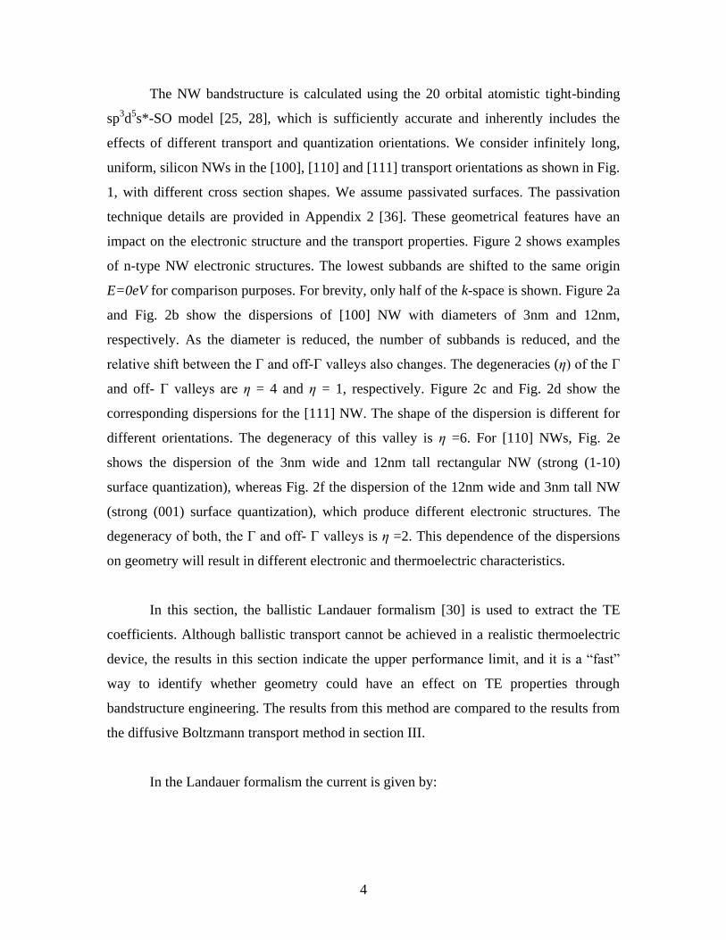
impact on the electronic structure and the transport properties. Figure 2 shows examples
of n-type NW electronic structures. The lowest subbands are shifted to the same origin
E=0eV for comparison purposes. For brevity, only half of the k-space is shown. Figure 2a
and Fig. 2b show the dispersions of [100] NW with diameters of 3nm and 12nm,
respectively. As the diameter is reduced, the number of subbands is reduced, and the
relative shift between the Γ and off-Γ valleys also changes. The degeneracies (η) of the Γ
and off- Γ valleys are η = 4 and η = 1, respectively. Figure 2c and Fig. 2d show the
corresponding dispersions for the [111] NW. The shape of the dispersion is different for
different orientations. The degeneracy of this valley is η =6. For [110] NWs, Fig. 2e
shows the dispersion of the 3nm wide and 12nm tall rectangular NW (strong (1-10)
surface quantization), whereas Fig. 2f the dispersion of the 12nm wide and 3nm tall NW
(strong (001) surface quantization), which produce different electronic structures. The
degeneracy of both, the Γ and off- Γ valleys is η =2. This dependence of the dispersions
on geometry will result in different electronic and thermoelectric characteristics.
In this section, the ballistic Landauer formalism [30] is used to extract the TE
coefficients. Although ballistic transport cannot be achieved in a realistic thermoelectric
device, the results in this section indicate the upper performance limit, and it is a “fast”
way to identify whether geometry could have an effect on TE properties through
bandstructure engineering. The results from this method are compared to the results from
the diffusive Boltzmann transport method in section III.
In the Landauer formalism the current is given by:
5
0 01 2
0 0
k k
k k
q qJ v f v f
L L
(1a)
01 2
0
,k
k
qv f f
L
(1b)
where vk is the bandstructure velocity, and f1, f2 are the Fermi functions of the left and
right contacts, respectively. Auxiliary functions R(α)
(f1, f2,T) can be defined as:
01 2 1
( ) 0
1 2
,k k
k
qv f f E
LR
(2)
where µ1, µ2 are the contact Fermi levels, and Ek is the subband dispersion relation. This
formula is the same as the one described in references [31, 37], where for small driving
fields ΔV, the linearization 11 2 0
ff f q V
E
is applied. Here, however, the
computation is explicitly performed in k-space rather than energy-space. From these
functions, the conductance G, the Seebeck coefficient S, and the electronic part of the
thermal conductivity κe, can be derived as
,0RG (3a)
,
10
1
R
R
TS (3b)
21
2
0
1.e
RR
T R
(3c)
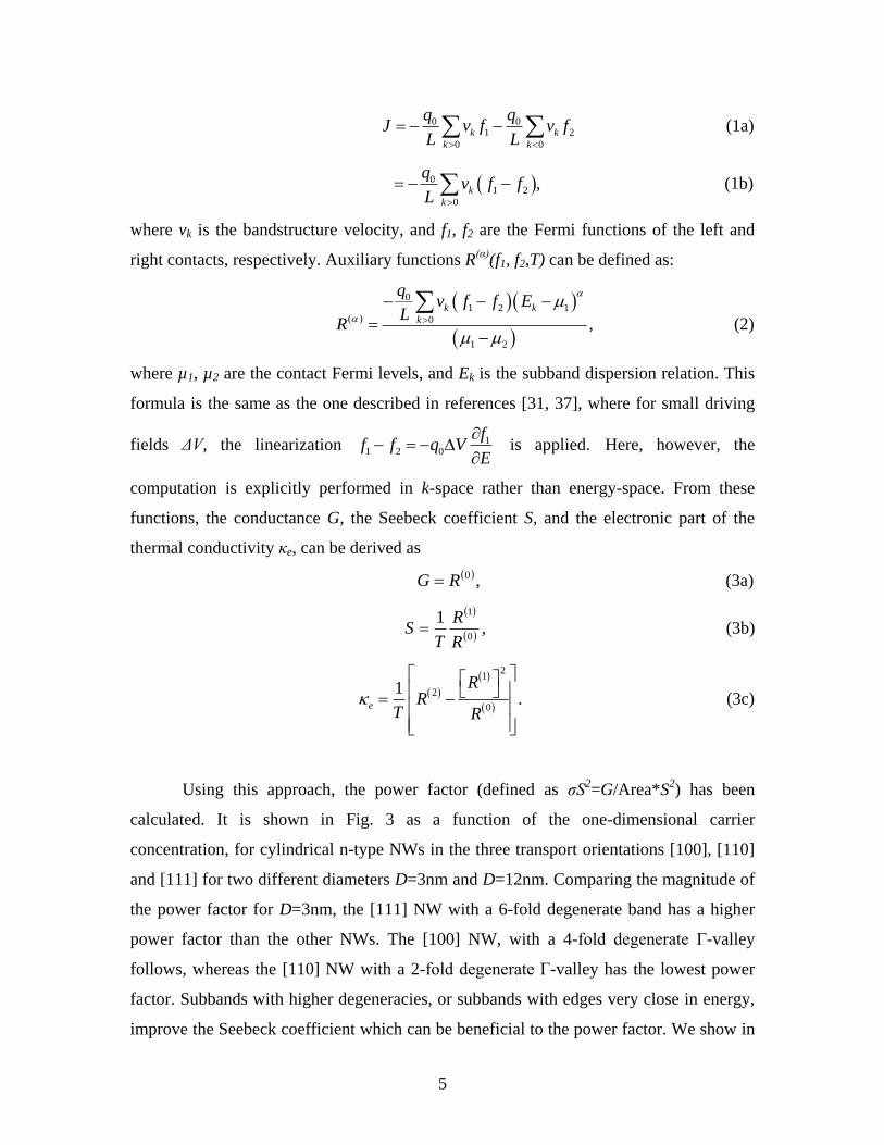
Using this approach, the power factor (defined as σS2=G/Area*S
2) has been
calculated. It is shown in Fig. 3 as a function of the one-dimensional carrier
concentration, for cylindrical n-type NWs in the three transport orientations [100], [110]
and [111] for two different diameters D=3nm and D=12nm. Comparing the magnitude of
the power factor for D=3nm, the [111] NW with a 6-fold degenerate band has a higher
power factor than the other NWs. The [100] NW, with a 4-fold degenerate Γ-valley
follows, whereas the [110] NW with a 2-fold degenerate Γ-valley has the lowest power
factor. Subbands with higher degeneracies, or subbands with edges very close in energy,
improve the Seebeck coefficient which can be beneficial to the power factor. We show in
6
section III, however, that once scattering is included in the calculation, the conductivity is
degraded, which turns out to be a more dominant effect than the increase in Seebeck
coefficient. For D=12nm in Fig. 3, the NW bandstructure becomes bulk-like, and any
orientation effects that existed because of the bandstructure differences in lower
diameters, are now smeared out. The interesting observation, however, is that under
ballistic conditions, it seems that it is possible to improve the thermoelectric power factor
by feature size scaling, in agreement with other theoretical ballistic transport studies, [31,
32, 33, 34]. The magnitude of these benefits, however, is only within a factor of two.
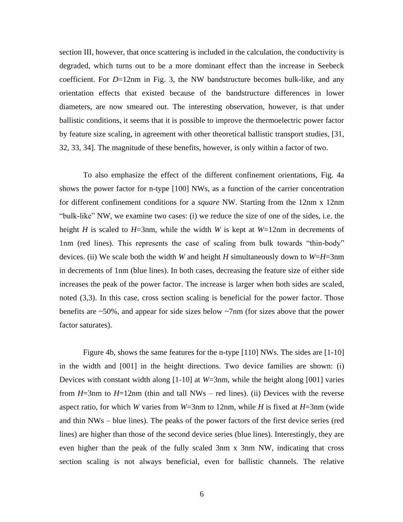
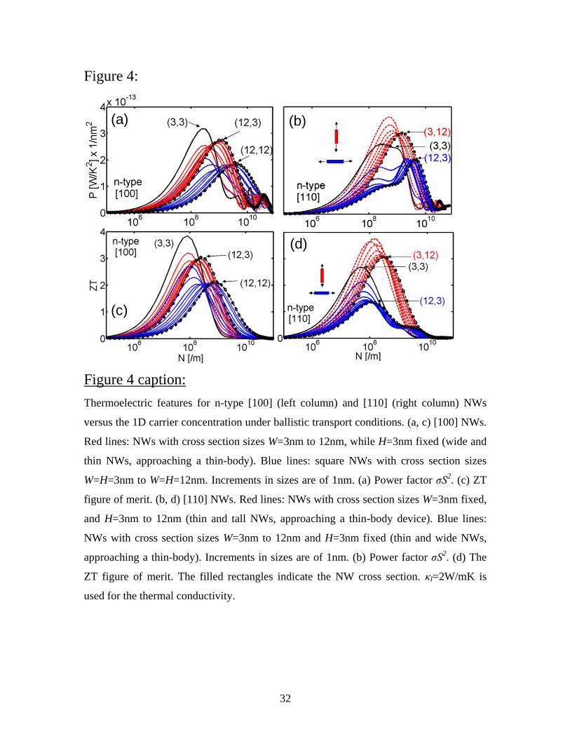
To also emphasize the effect of the different confinement orientations, Fig. 4a
shows the power factor for n-type [100] NWs, as a function of the carrier concentration
for different confinement conditions for a square NW. Starting from the 12nm x 12nm
“bulk-like” NW, we examine two cases: (i) we reduce the size of one of the sides, i.e. the
height H is scaled to H=3nm, while the width W is kept at W=12nm in decrements of
1nm (red lines). This represents the case of scaling from bulk towards “thin-body”
devices. (ii) We scale both the width W and height H simultaneously down to W=H=3nm
in decrements of 1nm (blue lines). In both cases, decreasing the feature size of either side
increases the peak of the power factor. The increase is larger when both sides are scaled,
noted (3,3). In this case, cross section scaling is beneficial for the power factor. Those
benefits are ~50%, and appear for side sizes below ~7nm (for sizes above that the power
factor saturates).
Figure 4b, shows the same features for the n-type [110] NWs. The sides are [1-10]
in the width and [001] in the height directions. Two device families are shown: (i)
Devices with constant width along [1-10] at W=3nm, while the height along [001] varies
from H=3nm to H=12nm (thin and tall NWs – red lines). (ii) Devices with the reverse
aspect ratio, for which W varies from W=3nm to 12nm, while H is fixed at H=3nm (wide
and thin NWs – blue lines). The peaks of the power factors of the first device series (red
lines) are higher than those of the second device series (blue lines). Interestingly, they are
even higher than the peak of the fully scaled 3nm x 3nm NW, indicating that cross
section scaling is not always beneficial, even for ballistic channels. The relative
7
performance in these channels, as in the case of the ones described in Fig. 3, originate
from the higher Seebeck coefficient, which is a consequence of the larger number of
subbands/degeneracies in the electronic structure of this nanowire near the conduction
band edge. The 3nm x 12nm NW has a higher performance than the 12nm x 3nm
because, as previously shown in Fig. 2e, the band edges of the Γ and off-Γ valleys are
nearby in energy. For the 12nm x 3nm NW in Fig. 2f, the off-Γ valleys are higher in
energy and do not participate in transport.
Figure 4c and Fig. 4d show the figure of merit ZT values of the devices in Fig. 4a
and Fig. 4b, respectively, using a single value of κl=2W/mK for the lattice part of the
thermal conductivity, which was experimentally demonstrated for NWs [13, 15, 18]. ZT
follows the shape and trends of the power factor. Interestingly, under ballistic
assumptions, very high ZT values up to 4 can be achieved. We emphasize that such a low
value for the thermal conductivity has experimentally only been achieved in rough or
distorted NWs. We still use it, however, although for electrons we consider ballistic
transport. Our intention here is to provide an idealized upper value for the ZT in Si NWs.
As we will describe later on in section IV, such values cannot be obtained once surface
roughness scattering is incorporated. On the other hand, other methods for achieving very
low thermal conductivity values have been theoretically proposed, which do not rely on
surface roughness. Markussen et al., has proposed that Si nanowires, having surfaces
decorated with molecules could also significantly reduce thermal conductivity, for which
case our results are more relevant [38].
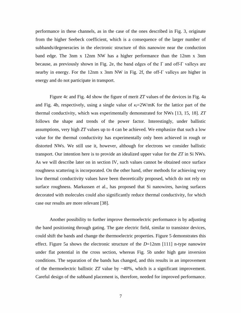
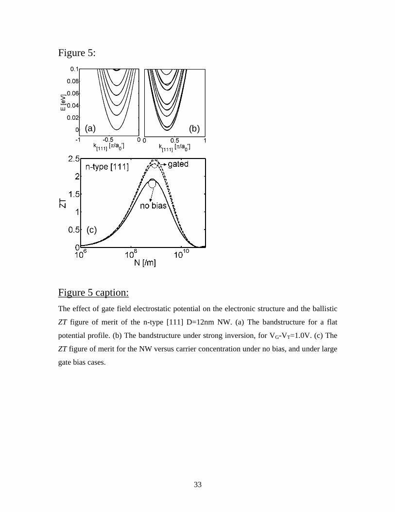
Another possibility to further improve thermoelectric performance is by adjusting
the band positioning through gating. The gate electric field, similar to transistor devices,
could shift the bands and change the thermoelectric properties. Figure 5 demonstrates this
effect. Figure 5a shows the electronic structure of the D=12nm [111] n-type nanowire
under flat potential in the cross section, whereas Fig. 5b under high gate inversion
conditions. The separation of the bands has changed, and this results in an improvement
of the thermoelectric ballistic ZT value by ~40%, which is a significant improvement.
Careful design of the subband placement is, therefore, needed for improved performance.
8
The nanostructure geometry enters the design through subband engineering. The tight-
binding (TB) model is particularly suited for this, because the computational domain can
be extended beyond 10nm, and the effect of length scale can be properly investigated.
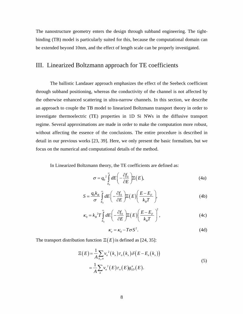
III. Linearized Boltzmann approach for TE coefficients
The ballistic Landauer approach emphasizes the effect of the Seebeck coefficient
through subband positioning, whereas the conductivity of the channel is not affected by
the otherwise enhanced scattering in ultra-narrow channels. In this section, we describe
an approach to couple the TB model to linearized Boltzmann transport theory in order to
investigate thermoelectric (TE) properties in 1D Si NWs in the diffusive transport
regime. Several approximations are made in order to make the computation more robust,
without affecting the essence of the conclusions. The entire procedure is described in
detail in our previous works [23, 39]. Here, we only present the basic formalism, but we
focus on the numerical and computational details of the method.
In Linearized Boltzmann theory, the TE coefficients are defined as:
0
2 00 ,
E
fq dE E
E
(4a)
0
0 0 ,B F
BE
q k f E ES dE E
E k T
(4b)
0
2
2 00 ,F
B
BE
f E Ek T dE E
E k T
(4c)
2
0 .e T S (4d)
The transport distribution function E is defined as [24, 35]:
2
,
2
1
1
1 .
x
n x n x n x
k n
n
n n D
n
E v k k E E kA
v E E g EA
(5)
9
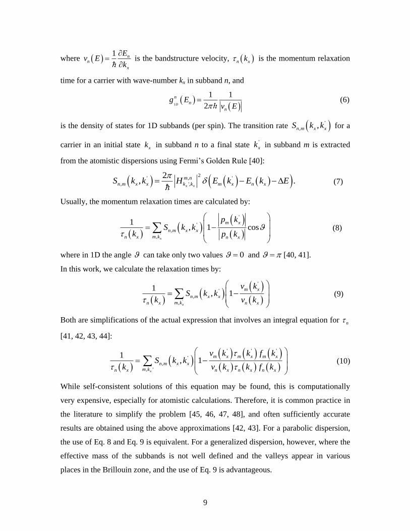
where 1 n
n
x
Ev E
k
is the bandstructure velocity, n xk is the momentum relaxation
time for a carrier with wave-number kx in subband n, and
1
1 1
2D
n
n
n
g Ev E
(6)
is the density of states for 1D subbands (per spin). The transition rate '
, ,n m x xS k k for a
carrier in an initial state xk in subband n to a final state '
xk in subband m is extracted
from the atomistic dispersions using Fermi’s Golden Rule [40]:
2
' , '
, ',
2, .
x x
m n
n m x x k k m x n xS k k H E k E k E
(7)
Usually, the momentum relaxation times are calculated by:
'
'
'
,
,
1, 1 cos
x
m x
n m x x
m kn x n x
p kS k k
k p k
(8)
where in 1D the angle can take only two values 0 and [40, 41].
In this work, we calculate the relaxation times by:
'
'
'
,
,
1, 1
x
m x
n m x x
m kn x n x
v kS k k
k v k
(9)
Both are simplifications of the actual expression that involves an integral equation for n
[41, 42, 43, 44]:
' ' '
'
,
, '
1, 1
x
m x m x m x
n m x x
m kn x n x n x n x
v k k f kS k k
k v k k f k
(10)
While self-consistent solutions of this equation may be found, this is computationally
very expensive, especially for atomistic calculations. Therefore, it is common practice in
the literature to simplify the problem [45, 46, 47, 48], and often sufficiently accurate
results are obtained using the above approximations [42, 43]. For a parabolic dispersion,
the use of Eq. 8 and Eq. 9 is equivalent. For a generalized dispersion, however, where the
effective mass of the subbands is not well defined and the valleys appear in various
places in the Brillouin zone, and the use of Eq. 9 is advantageous.
10
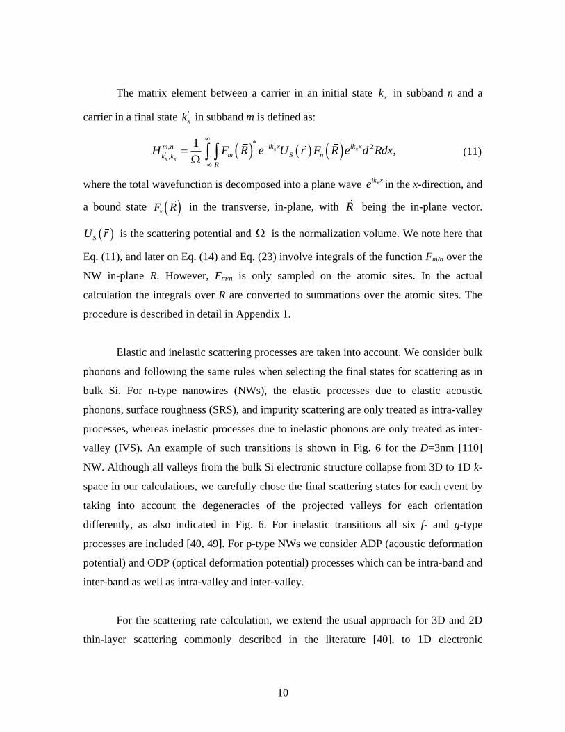
The matrix element between a carrier in an initial state xk in subband n and a
carrier in a final state '
xk in subband m is defined as:
'
'
*, 2
,
1,x x
x x
ik x ik xm n
m S nk k
R
H F R e U r F R e d Rdx
(11)
where the total wavefunction is decomposed into a plane wave xik xe in the x-direction, and
a bound state vF R in the transverse, in-plane, with R being the in-plane vector.
SU r is the scattering potential and is the normalization volume. We note here that
Eq. (11), and later on Eq. (14) and Eq. (23) involve integrals of the function Fm/n over the
NW in-plane R. However, Fm/n is only sampled on the atomic sites. In the actual
calculation the integrals over R are converted to summations over the atomic sites. The
procedure is described in detail in Appendix 1.
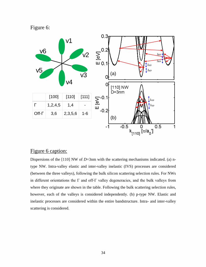
Elastic and inelastic scattering processes are taken into account. We consider bulk
phonons and following the same rules when selecting the final states for scattering as in
bulk Si. For n-type nanowires (NWs), the elastic processes due to elastic acoustic
phonons, surface roughness (SRS), and impurity scattering are only treated as intra-valley
processes, whereas inelastic processes due to inelastic phonons are only treated as inter-
valley (IVS). An example of such transitions is shown in Fig. 6 for the D=3nm [110]
NW. Although all valleys from the bulk Si electronic structure collapse from 3D to 1D k-
space in our calculations, we carefully chose the final scattering states for each event by
taking into account the degeneracies of the projected valleys for each orientation
differently, as also indicated in Fig. 6. For inelastic transitions all six f- and g-type
processes are included [40, 49]. For p-type NWs we consider ADP (acoustic deformation
potential) and ODP (optical deformation potential) processes which can be intra-band and
inter-band as well as intra-valley and inter-valley.
For the scattering rate calculation, we extend the usual approach for 3D and 2D
thin-layer scattering commonly described in the literature [40], to 1D electronic
11
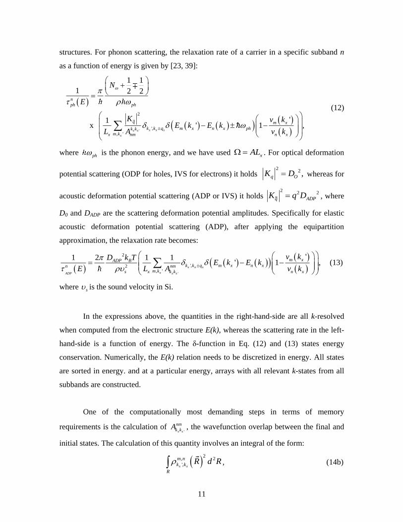
structures. For phonon scattering, the relaxation rate of a carrier in a specific subband n
as a function of energy is given by [23, 39]:
'
2
',
, '
1 1
1 2 2
'1 x ' 1 ,
x x xx x
x
n
ph ph
q m x
k k q m x n x phk km kx nm n x
N
E
K v kE k E k
L A v k
(12)
where ph is the phonon energy, and we have used xAL . For optical deformation
potential scattering (ODP for holes, IVS for electrons) it holds 2
2 ,q OK D whereas for
acoustic deformation potential scattering (ADP or IVS) it holds 2
2 2
q ADPK q D , where
D0 and DADP are the scattering deformation potential amplitudes. Specifically for elastic
acoustic deformation potential scattering (ADP), after applying the equipartition
approximation, the relaxation rate becomes:
'
2
',2, '
'1 2 1 1' 1 ,
x x x
xADP x x
m xADP Bk k q m x n xn nm
m ks x k k n x
v kD k TE k E k
E L A v k
(13)
where s is the sound velocity in Si.
In the expressions above, the quantities in the right-hand-side are all k-resolved
when computed from the electronic structure E(k), whereas the scattering rate in the left-
hand-side is a function of energy. The δ-function in Eq. (12) and (13) states energy
conservation. Numerically, the E(k) relation needs to be discretized in energy. All states
are sorted in energy. and at a particular energy, arrays with all relevant k-states from all
subbands are constructed.
One of the computationally most demanding steps in terms of memory
requirements is the calculation of 'x x
nm
k kA , the wavefunction overlap between the final and
initial states. The calculation of this quantity involves an integral of the form:
2
, 2
',x x
m n
k k
R
R d R , (14b)
12
*
,
', , ' ,x x x x
m n
k k m k n kR F R F R . (14b)
For the larger NWs, this calculation of the matrix elements imposes a huge computational
burden. All wavefunctions of every k-state for every subband need to be stored because it
is not known a priori for each initial state which are the corresponding final scattering k-
states and at which subbands when calculating the electronic structure, as indicated in the
scattering examples of Fig. 6. The D=12nm structures that could include 5500 atoms each
described by 20 orbitals, and a typical k-space grid of 200 points and considering 100
subbands, require several tens of Gbytes for the storage of the wavefunctions alone. For
computational efficiency, therefore, we use the following scheme: on each atom we add
the probability density of the components of each multi-orbital wavefunction, and
afterwards perform the final/initial state overlap multiplication. In such way, we
approximate the form factor components of a lattice atom at a specific location 0R by:
2, * *
', , , ' , , '
* *
, , , , ' , ' ,
, ,
2 2 2 2
, , ' , , '
x x x x x x
x x x x
x x x x
m n
k k n k m k n k m k
n k n k m k m k
n k m k n k m k
F F F F
F F F F
F F F F
(15)
where , run over the tight-binding orbitals of a specific atom. With this the overlaps
are computed using the probability density of each state, as in a single orbital (i.e.
effective mass) model, although we still keep the kx-dependence of the wavefunctions.
The approximation in Eq. 15 is important because it reduces the memory needed in the
computation by 20X, allowing simulations of large NW cross sections with only minimal
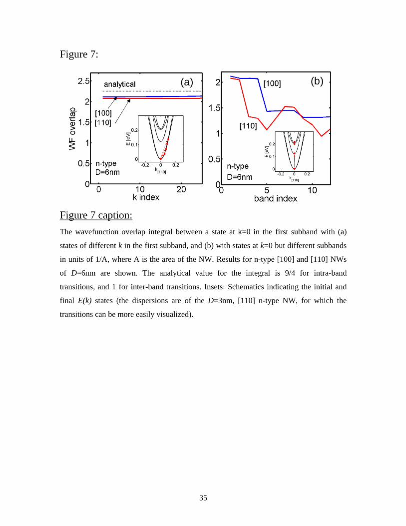
reduction in accuracy. Indeed, our numerical overlaps agree with the analytical
expressions for the wavefunction overlaps if one assumes sine or cosine wavefunctions
and parabolic bands, which can be derived to be 9 / 4A for intra-band and 1/ A for inter-
band transitions, where A is the cross section area of the NW [31, 40]. This is clearly
indicated in Fig. 7, where we show the wavefunction overlap for the n-type [100] and
[110] NWs with D=6nm between the state k=0, in subband n=1, and several final states in
units of 1/A. In Fig. 7a, the intra-band transitions are shown with final states in subband
m=1, and varying k-values. The wavefunction overlaps are indeed very close to the
13
analytical value of 9/4. In Fig. 7b, the inter-band transitions are shown with final states in
subbands m=1,2,…,12 and k=0. The first point, for m=1 is the intraband transition which
gives ~9/4, whereas for higher bands the overlaps reduce to lower values around ~1. The
values are very close to the analytical ones, do not have significant k-dependence, and
should not affect the qualitative nature of the results significantly. The price to pay,
however, is that with this simplification the phase information for the wavefunctions is
lost, and the selection rules are incorporated into the scattering rate calculation “by
hand”. However, this treatment is consistent with that for scattering in bulk and ultra-
thin-layer structures reported in the literature. Still, even after this simplification, the
storage of the probability density for the larger diameter NWs still requires several Giga
bytes of memory.
For surface roughness (SR), we assume a 1D exponential autocorrelation function
[50] for the roughness given by:
2 /2' CL
rmse
(16)
with Δrms = 0.48nm and LC = 1.3nm [48]. We derive the surface roughness matrix element
assuming that SR only causes a band edge shift. The scattering strength is given by the
shift in the subband edges with diameter scaling , /C VE D [51, 52]. The transition rate
is derived as:
2 2
0 ,' '
, 2 2
2 22, ,
2
C VSRS rms Cn m x x m x n x
x C
q E LS k k E k E k
D q L
(17)
where ' .x x xq k k As described by various authors, the band edge variation is the cause
of the major impact of SRS in ultra-scaled channels [48, 51, 52, 53, 54]. In Refs [48, 52]
it was shown that that the SRS limited low-field mobility in ultra-thin nanostructures
follows a L6 behavior, where L is the confinement length scale, originating from this
subband shift due to the variation of L. This SRS model is a simplified one, compared to
the ones described in Refs [48, 55, 56, 57] that account for additional Coulomb effects,
the wavefunction deformation at the interface, and the position of electrons in the
channel. These effects are ignored here since they only cause quantitative changes in our
14
results, whereas our focus is on qualitative trends that originate from geometry-induced
electronic structure variations.
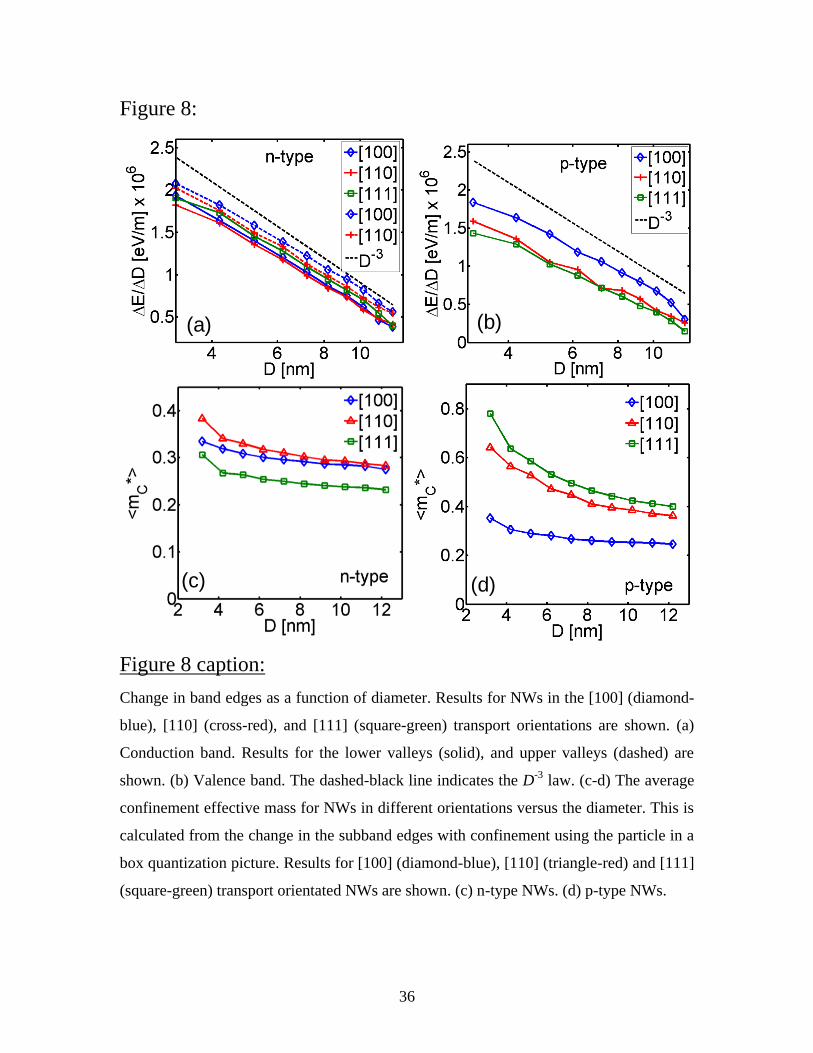
Figure 8a and Fig. 8b show the shift in the band edges /E D as a function of
diameter for the conduction and valence subbands, respectively. Indeed, the trends follow
a D-3
power law both for electrons and holes as expected, with some minor deviations.
For the n-type, the lowest valleys have slightly lower band edge shifts compared to the
higher valleys. In the calculation of the SRS, the Γ and off-Γ valleys are taken separately
into account when calculating the scattering rate. The orientation dependence is more
evident in the case of p-type NWs. The band edge shifts are larger for the [100] NWs,
whereas the band edges of the [111] NW are affected the least by diameter variations.
The sensitivity of the band edges can be directly correlated with a confinement effective
mass *
Cm . Using the simple notion of a particle in a box where the ground state energy is
2 2 * 2/ 2 CE m D , approximate values for *
Cm can be extracted. These are shown in Fig.
8c and Fig. 8d. For n-type NWs, the [110] orientation shows the largest *
Cm , whereas for
p-type NWs the [110] and [111] NWs have the largest *
Cm . The slight deviation in the
band edges from the D-3
law at smaller diameters, which reduces the rate of increase in
the scattering matrix element, are also reflected as an increase in the confinement
effective mass. The value of *
Cm of the n-type NWs lies between the longitudinal and
transverse bulk Si masses of ml=0.9m0 and mt=0.19m0. For p-type NWs, the *
Cm values
for the larger NW diameters are close to the bulk Si heavy-hole mass mhh=0.4m0. For the
[100] orientation they remain in that region for the smaller diameters as well. For the
[110] and [111] orientations on the other hand, *
Cm increases as the diameter is reduced.
This is an important observation that indicates that the p-type [111] and [110] NWs will
be less sensitive to surface roughness scattering (SRS). For thermoelectric materials this
can be especially important since SRS is needed for the reduction in thermal conductivity
κl. The fact that an intrinsic bandstructure mechanism makes the conductivity more
tolerant to SRS could help in power factor optimization in such channels in which rough
boundaries are favored.
15
For ionized impurity scattering the scattering potential is approximated by:
2 2' /2
0
220
,4
'
DR R x L
S
s
q eU r
R R x
(21)
where R is the position of an electron in the 2D cross section at 0x , influenced by an
impurity at , 'x R , and the x direction is assumed to extend to infinity. The 3D
screening length LD is given by:
1/20
2
0 3/2
.n
Fs BD
F
k TL
q
(22)
where F is the Fermi-Dirac integral of order α, and n is the carrier concentration.
The matrix element for electron-impurity scattering then becomes:
2 2' /2
, , ', 20',
220
1'
4'
Dxx x
x x
R R x Liq xn k m km n
k k
x sR
F R F Rq e eH R dx d R
LA AR R x
(23)
where the expression in the brackets is the Green’s function of the infinitely long channel
device. For a cylindrical channel, the expression in the parenthesis is the modified Bessel
function of second kind of order zero, 0 , 'K q R [48, 58, 59, 60].
The total transition rate due to impurity scattering is computed after taking the
square of the matrix element, multiplying by NILx, the number of impurities in the
normalized cross sectional area of the NW in the length of the unit cell, and integrating
over the distribution of impurities in the cross sectional area (over 'R ). The impurities are
assumed to be distributed uniformly in the volume considered.
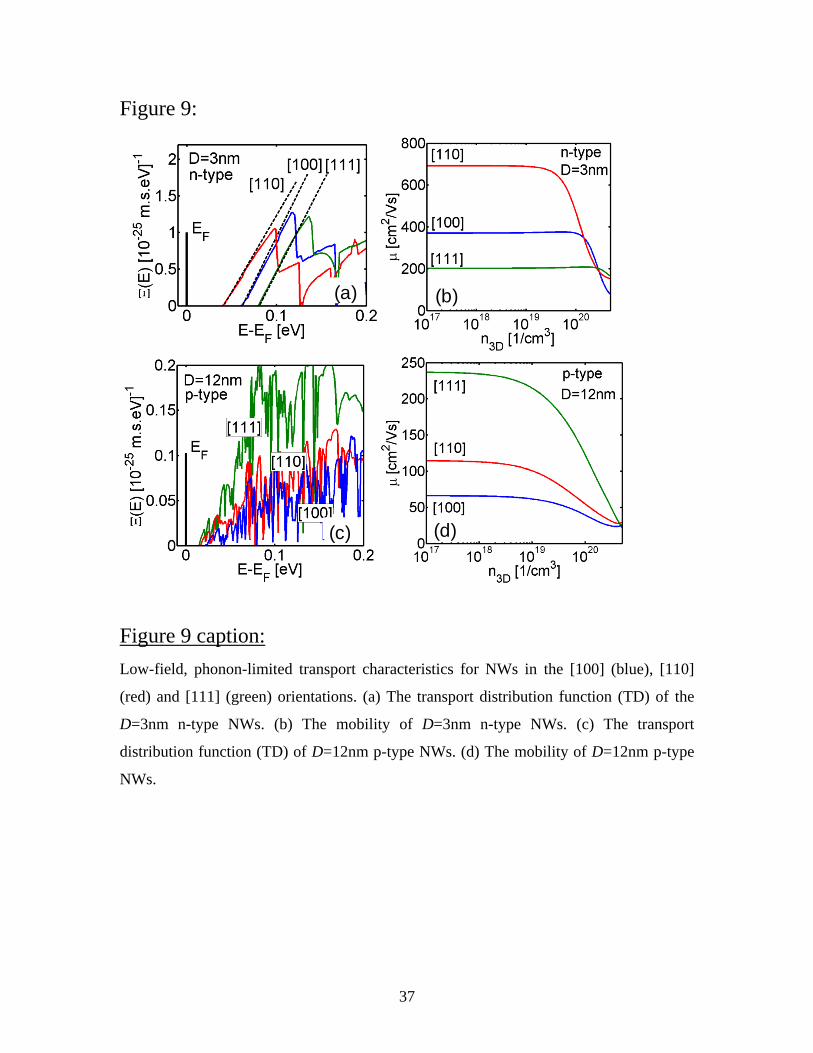
The transport distribution function (TD) in Eq. 5 turns out to be a very convenient
means to understand the effect of the electronic structure on the thermoelectric (TE)
coefficients. Figure 9a shows the phonon-limited TDs for n-type NWs of D=3nm. The
16
TDs for the three different orientations [100], [110] and [111] are shown. There are two
observations that determine the performance of the NWs. i) The low energy linear region,
where only one subband participates in transport, with slope proportional to */ m , where
is the degeneracy of the subband [39]. ii) The separation of the TD from the Fermi
level, F . The closer the TD is to the Fermi level for a particular carrier concentration
and the higher its slope, the larger the conductivity and mobility will be. This is shown in
Fig. 9b, where the orientation dependence of the mobility correlates with the order the
TDs appear with respect to the Fermi level. It is important to note that since the transport
and density-of-states (DOS) effective masses (m*) are the same for NWs, a reduction in
*m will not only reduce F in order to keep the carrier concentration fixed, but it will
also increase the TD slope, finally having a doubly positive impact on the conductivity
[39, 61]. Figure 9c shows a different situation, regarding the TDs for p-type NWs of
D=12nm in the three orientations. As the NW diameter increases, the DOS of the NWs
approaches the bulk DOS, and F is the same for all NWs. Their slope, however, is
different, which is reflected in the large anisotropy in the mobility in Fig. 9d. Note that
there are more subbands which result in more peaks in the TDs of the larger NWs
compared to the narrower ones.
As mentioned previously, one of the approximations used is that of bulk phonons.
Bulk phonons provide an ease of modeling and allow the understanding of the
bandstructure effects on the TE coefficients, still with good qualitative accuracy in the
results. Confined phonons in NWs can have very different dispersions and properties than
bulk. However, the effect of phonon confinement for the thinnest NWs examined in this
work is not that strong; it can be of the order of 10-20% (reduction in conductivity), and
declines fast as the diameter increases [45, 46, 47, 62]. In the literature it is common to
employ higher than bulk deformation potential values to account for phonon confinement
[48, 63, 64, 65]. Here we use deformation potential parameters 1013.24x10 eV / mholes
ODPD ,
5.34 eVholes
ADPD , and 9.5 eVelectrons
ADPD from Refs [45, 46, 61] which are more suitable
for NWs. All other electron-phonon coupling parameters are the bulk values taken from
[40]. The qualitative behavior of our results mostly depends on the shape of the
17
bandstructure and not on the strength of the phonon scattering mechanisms. For a more
quantitative description of the results, phonon confinement has to be accounted for.
However, even in that case, phonon scattering is not the major scattering mechanism in
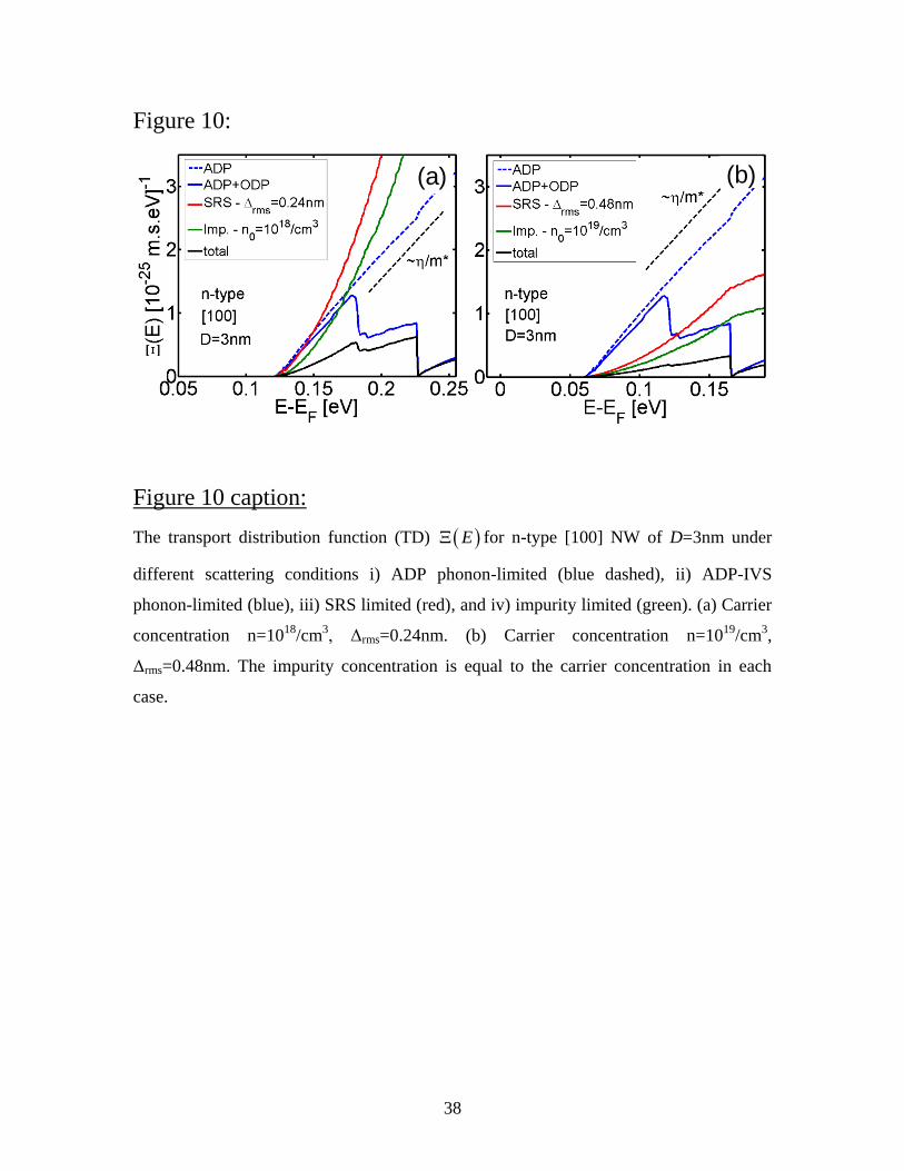
NW devices suited for TE applications. This is clearly demonstrated in Fig. 10, again
using the TD features for ADP-limited (blue-dotted), ADP-ODP-limited (blue-solid),
SRS-limited (red), impurity scattering-limited (green), and the TD including all scattering
mechanisms (black). In Fig. 10a moderate values for surface roughness (Δrms=0.24nm)
and impurity concentration (n0=1018
/cm3) are used. Strong scattering will lower the TD
value and degrade conductivity. From the important low energy region, we observe that
both SRS and impurity scattering mechanisms are stronger than phonon scattering. Figure
10b shows the same features, but with Δrms=0.48nm and n0=1019
/cm3, which are more
relevant for high performance thermoelectric devices (around the peak of the power
factor as it will be shown in section IV). SRS and impurity scattering are much stronger
than phonon scattering. A calculation of the phonon contribution to the total scattering
rate shows that it is only 12% and 6% in the situations of Fig. 10a and Fig. 10b,
respectively, even with the larger than bulk deformation potential values [23]. The
strongest mechanism is impurity scattering, which dominates the scattering processes at
such high concentrations. Indeed, this is in agreement with impurity scattering in bulk Si
which reduces the mobility by almost an order of magnitude from the phonon-limited
value at such high concentrations [66]. This shows that the details of phonon scattering
strength for NW devices might not be of great importance to the total channel
conductivity. This also demonstrates the importance of modulation doping in achieving
high thermoelectric performance.
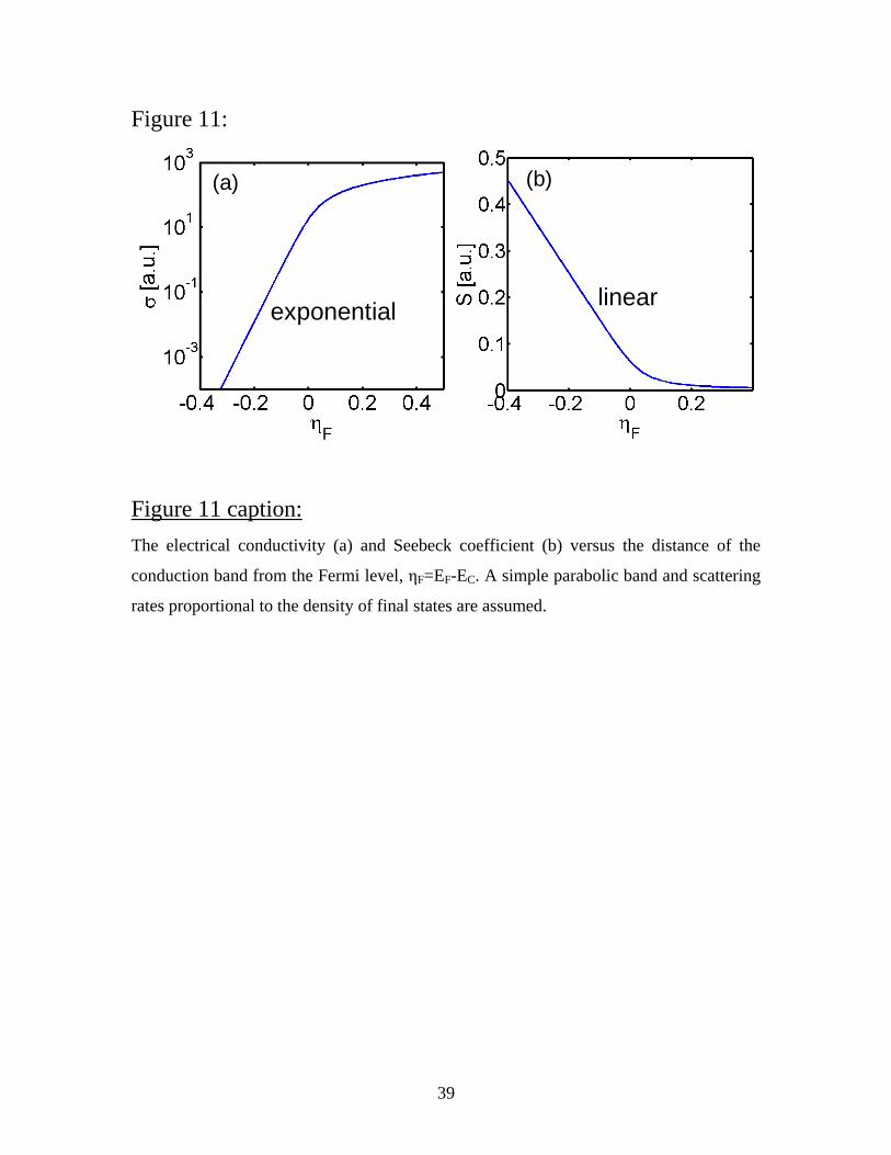
IV. Si nanowire thermoelectric coefficients
Geometrical features such as diameter and orientation will affect the electronic
structure, and influence the electrical conductivity and the Seebeck coefficient. If one
considers a specific carrier concentration, the influence of geometry shows up is two
ways: i) The band edges (or transport distribution functions TD) shift with respect to the
18
Fermi level as the geometry changes. ii) The effective masses (or carrier velocities)
change. The changes will be different for different NW cases. A change in F F CE E
will affect both the conductivity and the Seebeck coefficient. This effect is shown in Fig.
11a and Fig. 11b, respectively, using a simple 1D subband and effective mass
approximation. Changes in F affect the conductivity exponentially, but affect the
Seebeck coefficient only linearly, (and in an inverse way). The conductivity, therefore, is
affected much more than the Seebeck coefficient. At a specific carrier concentration,
changes in F can happen as follows: i) In a NW channel with only a few subbands, once
the diameter is reduced, F increases in order to keep the carrier concentration constant
as explained in detail in Refs [23, 39]. This reduces the conductivity exponentially. ii)
The DOS changes through electronic structure modifications and F will adjust to keep
the carrier concentration constant.
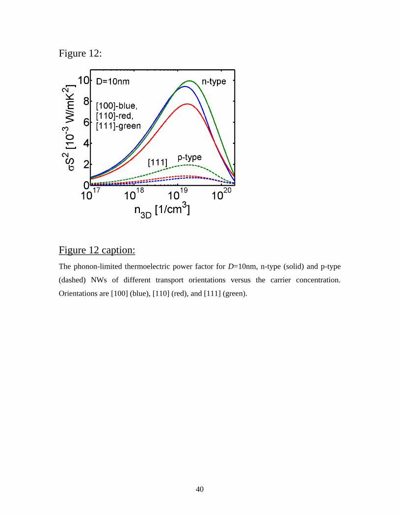
As a consequence, since the electronic structures of the NWs in different
orientations are different, F will differ as well, resulting in orientation and geometry
dependence of TE performance. Figure 12 shows the power factor for the n-type (solid)
and p-type (dashed) NWs with D=10nm, in the [100] (blue), [110] (red), and [111]
(green) transport orientations. The Boltzmann transport formalism was used. Some
orientation dependence can be observed. Especially in p-type NWs the [111] orientation
gives almost ~2X higher power factor than the other two p-type NW orientations. Note
that p-type NWs perform lower than the n-type NWs for this NW diameter, but this
difference is less severe for smaller diameters [23].
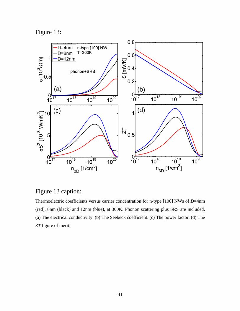
The conductivity usually degrades with diameter reduction because of the
enhancement of scattering mechanisms such as phonon and surface roughness scattering
(SRS) at smaller feature sizes. Figure 13 shows the effect of the diameter reduction on the
TE coefficients for the [100] n-type NW at room temperature. Phonon scattering and SRS
are considered. Figure 13a shows that the electrical conductivity decreases as the
diameter of the NW is reduced. On the other hand, the Seebeck coefficient in Fig. 13b
increases for the smaller diameters due to an F increase. Overall, the power factor in
19
Fig. 13c decreases with diameter, because the conductivity is degraded much more than
the Seebeck coefficient is improved. Using an experimentally measured value for the
thermal conductivity κl=2W/mK [15, 18], we compute the ZT figure of merit in Fig. 13d.
ZT is reduced with diameter reduction, following the trend in the power factor. Two
important observations can be made at this point: i) The conclusions are different from
what previously described in Fig. 3 and Fig. 4 for ballistic transport. The increase in the
power factor and ZT at reduced feature sizes is not observed when scattering is
incorporated. On the contrary, the performance is degraded, because of a reduction in the
conductivity. ii) ZT ~0.5-1 can be achieved in Si NWs, in agreement with recent
experimental measurements [12, 13] (reduced from ZT~4 under ballistic considerations in
Fig. 4). On the other hand, the value κl=2W/mK used for the calculation of ZT is
measured for Si NWs of diameters D=15nm [15, 18]. This might be even smaller for
smaller NW diameters or even orientation dependent [67, 68]. The power factor and ZT
could potentially change and higher performance could be achieved. Nevertheless, the
magnitude of these results is in agreement with other reports, both theoretical [37, 69]
and experimental [12, 13, 14, 65].
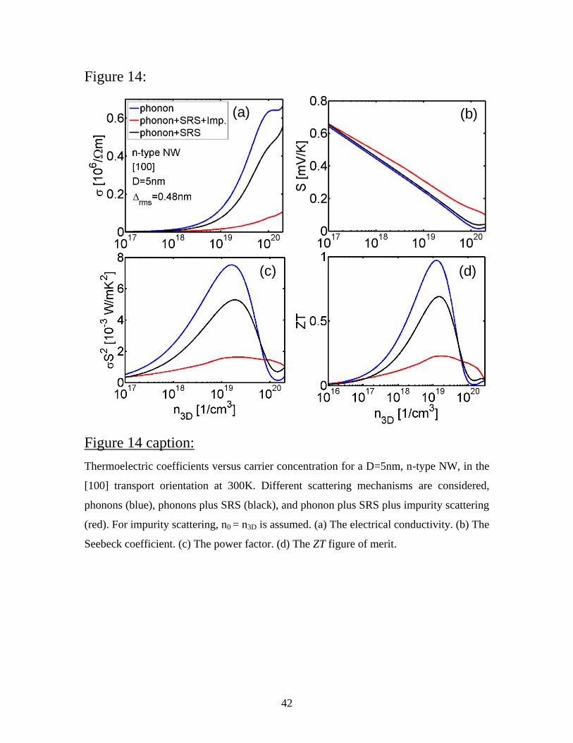
The results in Fig. 13 only consider phonon scattering and SRS. The peak of the
power factor, however, appears at carrier concentrations of 1019
/cm3. In order to reach
such concentration high doping levels are required and the effect of impurity scattering
thus cannot be excluded. In Fig. 14, we demonstrate the effect of different scattering
mechanisms for the n-type [100] NW of diameters D=5nm. The conductivity in Fig. 14a
is strongly degraded from the phonon-limited values (blue) once surface roughness
scattering-SRS (black) and most importantly impurity scattering (red) are included in the
calculation. The impurity concentration used at each instance is equal to the carrier
concentration. The Seebeck coefficient in Fig. 14b does not change significantly with the
introduction of additional scattering mechanisms because it is independent of scattering
at first order [31]. The conductivity dominates the power factor, which is drastically
reduced due to SRS and mostly impurity scattering (Fig. 14c). This can also reduce the
ZT as shown in Fig. 14d from ZT~1 down to ZT~0.2. Since impurity scattering is such a
20
strong mechanism, for high performance NW TEs alternative doping schemes need to be
employed such as modulation doping or charge transfer techniques [65, 70, 71, 72].
V. Conclusions
We presented a methodology that couples the atomistic sp3d
5s
*-SO tight-binding
model to two different transport formalisms: i) Landauer ballistic and ii) Linearized
Boltzmann theory for calculating the thermoelectric power factor in ultra-thin Si
nanowires. We introduced some approximations needed to make such methodology
robust and efficient, and explained the differences in the conclusions obtained from these
two different transport methods. Using this formalism the computational domain can be
extended to “large” feature sizes (>10nm) still accounting for all atomistic effects, so that
the length scale degree of freedom can be properly used as a design parameter. We show
that geometrical features such as cross section and orientations could potentially provide
optimization directions for the thermoelectric power factor in NWs. In the Si NWs
investigated, low-dimensionality and geometrical features affect the electrical
conductivity much more than the Seebeck coefficient. The conductivity is, therefore, the
quantity that controls the behavior of the power factor and the figure of merit ZT, in
contrast to the current view that the low-dimensional features could provide benefits
through improvements in the Seebeck coefficient. We finally show that impurity
scattering is the strongest scattering mechanism in nanowire thermoelectric channels, and
ways that allow high carrier concentration without direct doping could largely improve
the performance.
Acknowledgements
This work was supported by the Austrian Climate and Energy Fund, contract No. 825467.
21
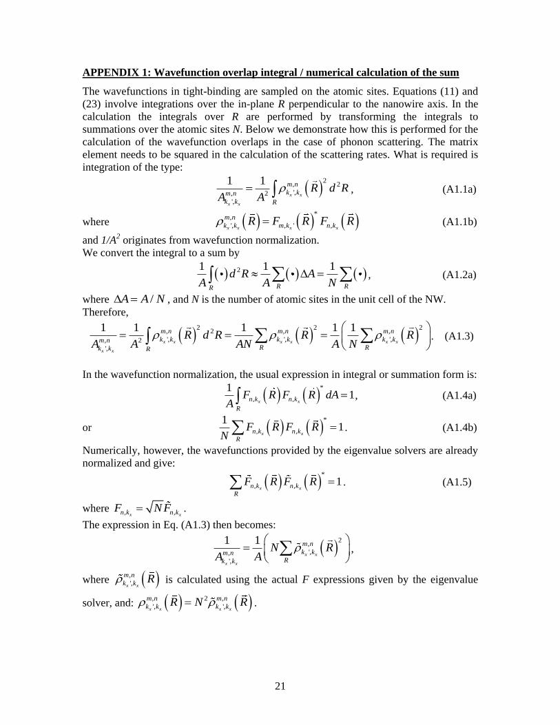
APPENDIX 1: Wavefunction overlap integral / numerical calculation of the sum
The wavefunctions in tight-binding are sampled on the atomic sites. Equations (11) and
(23) involve integrations over the in-plane R perpendicular to the nanowire axis. In the
calculation the integrals over R are performed by transforming the integrals to
summations over the atomic sites N. Below we demonstrate how this is performed for the
calculation of the wavefunction overlaps in the case of phonon scattering. The matrix
element needs to be squared in the calculation of the scattering rates. What is required is
integration of the type:
2
, 2
',, 2
',
1 1x x
x x
m n
k km n
k k R
R d RA A
, (A1.1a)
where *
,
', , ' ,x x x x
m n
k k m k n kR F R F R (A1.1b)
and 1/A2 originates from wavefunction normalization.
We convert the integral to a sum by
21 1 1
R RR
d R AA A N
, (A1.2a)
where /A A N , and N is the number of atomic sites in the unit cell of the NW.
Therefore,
2 2 2
, 2 , ,
', ', ',, 2
',
1 1 1 1 1x x x x x x
x x
m n m n m n
k k k k k km nR Rk k R
R d R R RA A AN A N
. (A1.3)
In the wavefunction normalization, the usual expression in integral or summation form is:
*
, ,
11
x xn k n k
R
F R F R dAA
, (A1.4a)
or *
, ,
11
x xn k n k
R
F R F RN
. (A1.4b)
Numerically, however, the wavefunctions provided by the eigenvalue solvers are already
normalized and give:
*
, , 1x xn k n k
R
F R F R . (A1.5)
where , ,x xn k n kF N F .
The expression in Eq. (A1.3) then becomes:
2
,
',,
',
1 1x x
x x
m n
k km nRk k
N RA A
,
where ,
',x x
m n
k k R is calculated using the actual F expressions given by the eigenvalue
solver, and: , 2 ,
', ',x x x x
m n m n
k k k kR N R .
22
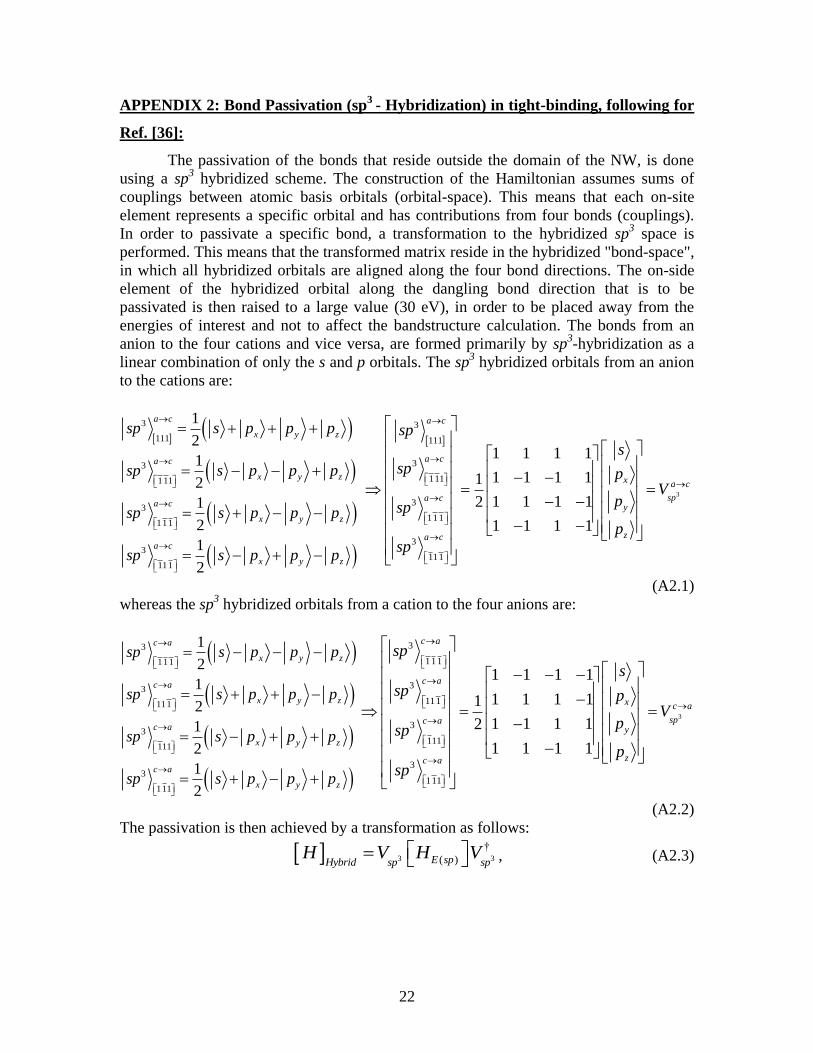
APPENDIX 2: Bond Passivation (sp3
- Hybridization) in tight-binding, following for
Ref. [36]:
The passivation of the bonds that reside outside the domain of the NW, is done
using a sp3 hybridized scheme. The construction of the Hamiltonian assumes sums of
couplings between atomic basis orbitals (orbital-space). This means that each on-site
element represents a specific orbital and has contributions from four bonds (couplings).
In order to passivate a specific bond, a transformation to the hybridized sp3 space is
performed. This means that the transformed matrix reside in the hybridized "bond-space",
in which all hybridized orbitals are aligned along the four bond directions. The on-side
element of the hybridized orbital along the dangling bond direction that is to be
passivated is then raised to a large value (30 eV), in order to be placed away from the
energies of interest and not to affect the bandstructure calculation. The bonds from an
anion to the four cations and vice versa, are formed primarily by sp3-hybridization as a
linear combination of only the s and p orbitals. The sp3 hybridized orbitals from an anion
to the cations are:
3
111
3
111
3
111
3
111
1
2
1
2
1
2
1
2
a c
x y z
a c
x y z
a c
x y z
a c
x y z
sp s p p p
sp s p p p
sp s p p p
sp s p p p
3
3
111
3
111
3
111
3
111
1 1 1 1
1 1 1 11
1 1 1 12
1 1 1 1
a c
a c
x a c
spa cy
za c
sp
s
sp pV
psp
psp
(A2.1)
whereas the sp3 hybridized orbitals from a cation to the four anions are:
3
111
3
111
3
111
3
111
1
2
1
2
1
2
1
2
c a
x y z
c a
x y z
c a
x y z
c a
x y z
sp s p p p
sp s p p p
sp s p p p
sp s p p p
3
3
111
3
111
3
111
3
111
1 1 1 1
1 1 1 11
1 1 1 12
1 1 1 1
c a
c a
x c a
spc ay
zc a
sp
s
sp pV
psp
psp
(A2.2)
The passivation is then achieved by a transformation as follows:
3 3
†
( )E spHybrid sp spH V H V , (A2.3)
23
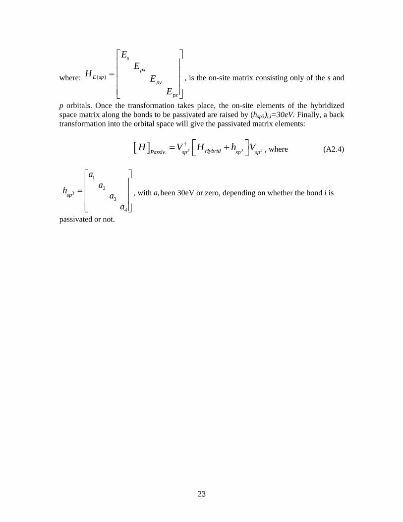
where: ( )
s
px
E sppy
pz
E
EH
E
E
, is the on-site matrix consisting only of the s and
p orbitals. Once the transformation takes place, the on-site elements of the hybridized
space matrix along the bonds to be passivated are raised by (hsp3)i,i=30eV. Finally, a back
transformation into the orbital space will give the passivated matrix elements:
3 3 3
†
. HybridPassiv sp sp spH V H h V
, where (A2.4)
3
1
2
3
4
sp
a
ah
a
a
, with ai been 30eV or zero, depending on whether the bond i is
passivated or not.
24
References
[1] G. J. Snyder and E. S. Toberer, Nature Materials, vol. 7, pp. 105–114, 2008.
[2] A. Majumdar, Science Materials, vol. 303, pp. 777–778, 2004.
[3] L.D. Hicks, and M. S. Dresselhaus, Phys. Rev. B, vol. 47, no. 24, p. 16631, 1993.
[4] R. Venkatasubramanian, E. Siivola, T. Colpitts, and B. O’ Quinn, Nature, vol. 413,
pp. 597-602, 2001.
[5] D. A. Broido and T. L. Reinecke, Phys. Rev. B, vol. 51, p. 13797, 1994.
[6] T. C. Harman, P. J. Taylor, M. P. Walsh, and B. E. LaForge, Science, 297, 2229–
2232, 2002.
[7] M. Dresselhaus, G. Chen, M. Y. Tang, R. Yang, H. Lee, D. Wang, Z. Ren, J.-P.
Fleurial, and P. Gagna, Adv. Mater., vol. 19, pp. 1043-1053, 2007.
[8] A. Shakouri, IEEE International Conference on thermoelectrics, pp. 495–500, 2005.
[9] J. O. Sofo and G. D. Mahan, Appl. Phys. Lett., vol. 65, p. 2690 (3pp), 1994.
[10] W. Kim, S. L. Singer, A. Majumdar, D. Vashaee, Z. Bian, A. Shakouri, G. Zeng, J.
E. Bowers, J. M. O. Zide, and A. C. Gossard, Appl. Phys. Lett., vol. 88, p. 242107, 2006.
[11] Y. Wu, R. Fan, and P. Yang, Nano Lett., vol. 2, no. 2, pp. 83-83, 2002.
[12] A. I. Boukai, Y. Bunimovich, J. T.-Kheli, J.-K. Yu, W. A. G. III, and J. R. Heath,
Nature, 451, 168–171, 2008.
[13] A. I. Hochbaum, R. Chen, R. D. Delgado, W. Liang, E. C. Garnett, M. Najarian, A.
Majumdar, and P. Yang, Nature, vol. 451, pp. 163–168, 2008.
[14] J. Tang, H.-T. Wang, D. H. Lee, M. Fardy, Z. Huo, T. P. Russell, and P. Yang, Nano
Lett., 10, 10, 4279-4283, 2010.
[15] D. Li, Y. Wu, R. Fang, P. Yang, and A. Majumdar Appl. Phys. Lett., 83, 3186–3188,
2003.
[16] K. Nielsch, J. Bachmann , J. Kimling , and H. Böttner, Adv. Energy Mater., 1, 713,
2011.
[17] G. Chen, Semiconductors and Semimetals, vol. 71, pp. 203–259, 2001.
25
[18] R. Chen, A. I. Hochbaum, P. Murphy, J. Moore, P. Yang, and A. Majumdar, Phys.
Rev. Lett., vol. 101, p. 105501, 2008.
[19] D. Li, S. T. Huxtable, A. R. Abramsin, and A. Majumdar, Trans. of the ASME, 127,
108–114, 2005.
[20] P. Martin, Z. Aksamija, E. Pop, and U. Ravaioli, Phys. Rev. Lett., 102, 125503,
2009.
[21] C. J. Vineis, A. Shakouri, A. Majumdar, and M. C. Kanatzidis, Adv. Mater., 22,
3970-3980, 2010.
[22] C. M. Jaworski, V. Kulbachinskii, and J. P. Heremans, Phys. Rev. B, 80, 125208,
2009.
[23] N. Neophytou and H. Kosina, Phys. Rev. B, vol. 83, 245305, 2011.
[24] G. D. Mahan and J. O. Sofo, Proc. Natl. Acad. Sci. USA, vol. 93, pp. 7436-7439,
1996.
[25] T. B. Boykin, G. Klimeck, and F. Oyafuso, Phys. Rev. B, vol. 69, no. 11, pp.
115201-115210, 2004.
[26] G. Klimeck, S. Ahmed, B. Hansang, N. Kharche, S. Clark, B. Haley, S. Lee, M.
Naumov, H. Ryu, F. Saied, M. Prada, M. Korkusinski, T. B. Boykin, and R. Rahman,
IEEE Trans. Electr. Dev., vol. 54, no. 9, pp. 2079-2089, 2007.
[27] G. Klimeck, S. Ahmed, N. Kharche, M. Korkusinski, M. Usman, M. Prada, and T.
B. Boykin, IEEE Trans. Electr. Dev., vol. 54, no. 9, pp. 2090-2099, 2007.
[28] N. Neophytou, A. Paul, M. Lundstrom, and G. Klimeck, IEEE Trans. Elect. Dev.,
vol. 55, no. 6, pp. 1286-1297, 2008.
[29] N. Neophytou, A. Paul, and G. Klimeck, IEEE Trans. Nanotechnol., vol. 7, no. 6,
pp. 710-719, 2008.
[30] R. Landauer, IBM J. Res. Dev., vol. 1, p. 223, 1957.
[31] R. Kim, S. Datta, and M. S. Lundstrom, J. Appl. Phys., vol. 105, p. 034506, 2009.
[32] C. Jeong, R. Kim, M. Luisier, S. Datta, and M. Lundstrom, J. Appl. Phys. 107,
023707 2010.
[33] G. Liang, W. Huang, C. S. Koong, J.-S. Wang, and J. Lan, J. Appl. Phys. 107,
014317, 2010.
26
[34] N. Neophytou, M. Wagner, H. Kosina, and S. Selberherr, J. Electr. Materials, vol.
39, no. 9, pp. 1902-1908, 2010.
[35] T. J. Scheidemantel, C. A.-Draxl, T. Thonhauser, J. V. Badding, and J. O. Sofo,
Phys. Rev. B, vol. 68, p. 125210, 2003.
[36] S. Lee, F. Oyafuso, P. Von, Allmen, and G. Klimeck, Phys. Rev. B, vol. 69, pp.
045316-045323, 2004.
[37] T. T.M. Vo, A. J. Williamson, V. Lordi, and G. Galli, Nano Lett., vol. 8, no. 4, pp.
1111-1114, 2008.
[38] T. Markussen, A.-P. Jauho, and M. Brandbyge, Phys. Rev. Lett., vol. 103, p.
055502, 2009.
[39] N. Neophytou and H. Kosina, Phys. Rev. B, vol. 84, p. 085313, 2011.
[40] M. Lundstrom, “Fundamentals of Carrier Transport,” Cambridge University Press,
2000.
[41] D. K. Ferry and S. M. Goodnick, “Transport in Nanostructures,” Cambridge
University Press, 1997.
[42] M. V. Fischetti, J. Appl. Phys., 89, 1232, 2001.
[43] M. V. Fischetti, Z. Ren, P. M. Solomon, M. Yang, and K. Rim, J. Appl. Phys., 94,
1079, 2003.
[44] D. Esseni and A. Abramo, IEEE Trans. Electr. Dev., 50, 7, 1665, 2003.
[45] A. K. Buin, A. Verma, A. Svizhenko, and M. P. Anantram, Nano Lett., vol. 8, no. 2,
pp. 760-765, 2008.
[46] A. K. Buin, A. Verma, and M. P. Anantram, J. Appl. Phys., vol. 104, p. 053716,
2008.
[47] E. B. Ramayya, D. Vasileska, S. M. Goodnick, and I. Knezevic, J. Appl. Phys., vol.
104, p. 063711, 2008.
[48] S. Jin, M. V. Fischetti, and T. Tang, Jour. Appl. Phys., 102, 83715, 2007.
[49] C. Jacoboni and L. Reggiani, Rev. Mod. Phys., vol. 55, 645, 1983.
[50] S. M. Goodnick, D. K. Ferry, C. W. Wilmsen, Z. Liliental, D. Fathy, and O. L.
Krivanek, Phys. Rev. B, vol. 32, p. 8171, 1985.
27
[51] H. Sakaki, T. Noda, K. Hirakawa, M. Tanaka, and T. Matsusue, Appl. Phys. Lett.,
vol 51, no. 23, p. 1934, 1987.
[52] K. Uchida and S. Takagi, Appl. Phys. Lett., vol. 82, no. 17, pp. 2916-2918, 2003.
[53] T. Fang, A. Konar, H. Xing, and D. Jena, Phys. Rev. B, 78, 205403, 2008.
[54] J. Wang, E. Polizzi, A. Ghosh, S. Datta, and M. Lundstrom, Appl. Phys. Lett., 87,
043101, 2005.
[55] R. E. Prange and T.-W. Nee, Phys. Rev., vol. 168, 779, 1968.
[56] T. Ando, A. Fowler, and F. Stern, Rev. Mod. Phys., vol. 54, p. 437, 1982.
[57] D. Esseni, IEEE Trans. Electr. Dev., vol. 51, no. 3, p. 394, 2004.
[58] J. Lee and H. N. Spector, J. Appl. Phys., vol. 57, no. 2, p. 366, 1985.
[59] S. D. Sarma and W. Lai, Phys. Rev. B, vol. 32, no. 2, p. 1401, 1985.
[60] P. Yuh and K. L. Wang, Appl. Phys. Lett., vol. 49, no. 25, p. 1738, 1986.
[61] N. Neophytou and H. Kosina, Nano Lett., vol. 10, no. 12, pp. 4913-4919, 2010.
[62] L. Donetti, F. Gamiz, J. B. Roldan, and A. Godoy, J. Appl. Phys., vol. 100, p.
013701, 2006.
[63] M. V. Fischetti and S. E. Laux, J. Appl. Phys., 80, 2234, 1996.
[64] T. Yamada and D. K. Ferry, Solid-State Electron., 38, 881, 1995.
[65] H. J. Ryu, Z. Aksamija, D. M. Paskiewicz, S. A. Scott, M. G. Lagally, I. Knezevic,
and M. A. Eriksson, Phys. Rev. Lett., vol. 105, p. 256601, 2010.
[66] H. Kosina and G. Kaiblinger-Grujin, Solid-State Electronics, vol. 42, no. 3, pp. 331-
338, 1998.
[67] T. Markussen, A.-P. Jauho, and M. Brandbyge, Nano Lett., vol. 8, no. 11, pp. 3771-
3775, 2008.
[68] Z. Aksamija and I. Knezevic, Phys. Rev. B, 82, 045319, 2010.
[69] T. Markussen, A.-P. Jauho, and M. Brandbyge, Phys. Rev. B, 79, 035415, 2009.
[70] S. Goswami, C. Siegert, S. Shamim, M. Pepper, I. Farrer, D. A. Ritchie, and A.
Ghosh, Appl. Phys. Lett., 97, 132104, 2010.
28
[71] P. Zhang, E. Tewaarwerk, B.-N. Park, D. E. Savage, G. K. Celler, I. Knezevic, P. G.
Evans, M. A. Eriksson, and M. G. Lagally, Nature Lett., 439, 703, 2006.
[72] T. He, J. He, M. Lu, B. Chen, H. Pan, W. F. Reus, W. M. Nolte, D. P. Nackashi, P.
D. Franzon, and J. M. Tour, J. Am. Chem. Soc., 128, 14537, 2006.
29
Figure 1:
[100] [110] [111]
Figure 1 caption:
Zincblende lattice of cylindrical nanowires in the [100], [110], and [111] orientations.
30
Figure 2:
(a) (b)
(c) (d)
(e) (f)
Figure 2 caption:
Dispersions of n-type NWs in various orientations and diameters/side lengths. (a) [100],
D=3nm. (b) [100], D=12nm. (c) [111], D=3nm. (d) [111], D=12nm. (e-f) Dispersions of
rectangular NWs with widths (W) and heights (H): (e) [110] NW, W=3nm, H=12nm. (f)
[110] NW, W=12nm, H=3nm. a0, a0’ and a0’’ are the unit cell lengths for the wires in the
[100], [110], and [111] orientations, respectively. The filled rectangles indicate the NW
cross section.
31
Figure 3:
Figure 3 caption:
The thermoelectric power factor versus the 1D carrier concentration under ballistic
transport conditions for n-type NWs of D=3nm and D=12nm in the [100] (blue), [110]
(red), and [111] (green) orientations.
32
Figure 4:
(b)(a)
(d)
(c)
Figure 4 caption:
Thermoelectric features for n-type [100] (left column) and [110] (right column) NWs
versus the 1D carrier concentration under ballistic transport conditions. (a, c) [100] NWs.
Red lines: NWs with cross section sizes W=3nm to 12nm, while H=3nm fixed (wide and
thin NWs, approaching a thin-body). Blue lines: square NWs with cross section sizes
W=H=3nm to W=H=12nm. Increments in sizes are of 1nm. (a) Power factor σS2. (c) ZT
figure of merit. (b, d) [110] NWs. Red lines: NWs with cross section sizes W=3nm fixed,
and H=3nm to 12nm (thin and tall NWs, approaching a thin-body device). Blue lines:
NWs with cross section sizes W=3nm to 12nm and H=3nm fixed (thin and wide NWs,
approaching a thin-body). Increments in sizes are of 1nm. (b) Power factor σS2. (d) The
ZT figure of merit. The filled rectangles indicate the NW cross section. κl=2W/mK is
used for the thermal conductivity.
33
Figure 5:
(a) (b)
(c)
Figure 5 caption:
The effect of gate field electrostatic potential on the electronic structure and the ballistic
ZT figure of merit of the n-type [111] D=12nm NW. (a) The bandstructure for a flat
potential profile. (b) The bandstructure under strong inversion, for VG-VT=1.0V. (c) The
ZT figure of merit for the NW versus carrier concentration under no bias, and under large
gate bias cases.
34
Figure 6:
(a)
(b)
v1
v2
v3v4
v5
v6
[100] [110] [111]
Γ 1,2,4,5 1,4 -
Off-Γ 3,6 2,3,5,6 1-6
Figure 6 caption:
Dispersions of the [110] NW of D=3nm with the scattering mechanisms indicated. (a) n-
type NW. Intra-valley elastic and inter-valley inelastic (IVS) processes are considered
(between the three valleys), following the bulk silicon scattering selection rules. For NWs
in different orientations the Γ and off-Γ valley degeneracies, and the bulk valleys from
where they originate are shown in the table. Following the bulk scattering selection rules,
however, each of the valleys is considered independently. (b) p-type NW. Elastic and
inelastic processes are considered within the entire bandstructure. Intra- and inter-valley
scattering is considered.
35
Figure 7:
(b)(a)
Figure 7 caption:
The wavefunction overlap integral between a state at k=0 in the first subband with (a)
states of different k in the first subband, and (b) with states at k=0 but different subbands
in units of 1/A, where A is the area of the NW. Results for n-type [100] and [110] NWs
of D=6nm are shown. The analytical value for the integral is 9/4 for intra-band
transitions, and 1 for inter-band transitions. Insets: Schematics indicating the initial and
final E(k) states (the dispersions are of the D=3nm, [110] n-type NW, for which the
transitions can be more easily visualized).
36
Figure 8:
(a) (b)
(c) (d)
Figure 8 caption:
Change in band edges as a function of diameter. Results for NWs in the [100] (diamond-
blue), [110] (cross-red), and [111] (square-green) transport orientations are shown. (a)
Conduction band. Results for the lower valleys (solid), and upper valleys (dashed) are
shown. (b) Valence band. The dashed-black line indicates the D-3
law. (c-d) The average
confinement effective mass for NWs in different orientations versus the diameter. This is
calculated from the change in the subband edges with confinement using the particle in a
box quantization picture. Results for [100] (diamond-blue), [110] (triangle-red) and [111]
(square-green) transport orientated NWs are shown. (c) n-type NWs. (d) p-type NWs.
37
Figure 9:
(a) (b)
(c) (d)
Figure 9 caption:
Low-field, phonon-limited transport characteristics for NWs in the [100] (blue), [110]
(red) and [111] (green) orientations. (a) The transport distribution function (TD) of the
D=3nm n-type NWs. (b) The mobility of D=3nm n-type NWs. (c) The transport
distribution function (TD) of D=12nm p-type NWs. (d) The mobility of D=12nm p-type
NWs.
38
Figure 10:
(a) (b)
Figure 10 caption:
The transport distribution function (TD) E for n-type [100] NW of D=3nm under
different scattering conditions i) ADP phonon-limited (blue dashed), ii) ADP-IVS
phonon-limited (blue), iii) SRS limited (red), and iv) impurity limited (green). (a) Carrier
concentration n=1018
/cm3, Δrms=0.24nm. (b) Carrier concentration n=10
19/cm
3,
Δrms=0.48nm. The impurity concentration is equal to the carrier concentration in each
case.
39
Figure 11:
exponentiallinear
(a) (b)
Figure 11 caption:
The electrical conductivity (a) and Seebeck coefficient (b) versus the distance of the
conduction band from the Fermi level, ηF=EF-EC. A simple parabolic band and scattering
rates proportional to the density of final states are assumed.
40
Figure 12:
Figure 12 caption:
The phonon-limited thermoelectric power factor for D=10nm, n-type (solid) and p-type
(dashed) NWs of different transport orientations versus the carrier concentration.
Orientations are [100] (blue), [110] (red), and [111] (green).
41
Figure 13:
(a) (b)
(c) (d)
Figure 13 caption:
Thermoelectric coefficients versus carrier concentration for n-type [100] NWs of D=4nm
(red), 8nm (black) and 12nm (blue), at 300K. Phonon scattering plus SRS are included.
(a) The electrical conductivity. (b) The Seebeck coefficient. (c) The power factor. (d) The
ZT figure of merit.
42
Figure 14:
(a) (b)
(c) (d)
Figure 14 caption:
Thermoelectric coefficients versus carrier concentration for a D=5nm, n-type NW, in the
[100] transport orientation at 300K. Different scattering mechanisms are considered,
phonons (blue), phonons plus SRS (black), and phonon plus SRS plus impurity scattering
(red). For impurity scattering, n0 = n3D is assumed. (a) The electrical conductivity. (b) The
Seebeck coefficient. (c) The power factor. (d) The ZT figure of merit.


![Large thermoelectric power factor in p-type Si (110)/[110 ... · Large thermoelectric power factor in p-type Si (110)/[110] ultra-thin-layers compared to differently oriented channels](https://img.pdfslide.net/doc/110x75/5d1cafe188c993d66e8d65b4/large-thermoelectric-power-factor-in-p-type-si-110110-large-thermoelectric.jpg)