Embed Size (px)
Citation preview

NuMicro NUC131 Series Datasheet
Oct 31, 2014 Page 1 of 75 Revision 1.00
NU
MIC
RO
™ N
UC
13
1 S
ER
IES
DA
TA
SH
EE
T
NuMicro™ NUC131 Series
Datasheet
The information described in this document is the exclusive intellectual property of Nuvoton Technology Corporation and shall not be reproduced without permission from Nuvoton.
Nuvoton is providing this document only for reference purposes of NuMicroTM
microcontroller based system design. Nuvoton assumes no responsibility for errors or omissions.
All data and specifications are subject to change without notice.
For additional information or questions, please contact: Nuvoton Technology Corporation.
www.nuvoton.com

NuMicro NUC131 Series Datasheet
Oct 31, 2014 Page 2 of 75 Revision 1.00
NU
MIC
RO
™ N
UC
13
1 S
ER
IES
DA
TA
SH
EE
T
TABLE OF CONTENTS
1 GENERAL DESCRIPTION ..................................................................................... 7
2 FEATURES ............................................................................................................ 8
3 ABBREVIATIONS ................................................................................................ 11
4 PARTS INFORMATION LIST AND PIN CONFIGURATION ................................ 12
4.1 NuMicro MUC131 Series Selection Code ................................................. 12
4.2 NuMicro NUC131 Series Selection Guide ................................................. 13
4.3 Pin Configuration ................................................................................ 14
4.3.1 NuMicro NUC131 Pin Diagram .................................................................. 14
4.4 Pin Description .................................................................................. 16
4.4.1 NuMicro NUC131 Pin Description ............................................................... 16
5 BLOCK DIAGRAM ............................................................................................... 22
5.1 NuMicro NUC131 Block Diagram ........................................................... 22
6 FUNCTIONAL DESCRIPTION ............................................................................. 23
6.1 ARM® Cortex™-M0 Core ...................................................................... 23
6.2 System Manager ................................................................................ 25
6.2.1 Overview .............................................................................................. 25
6.2.2 System Reset ........................................................................................ 25
6.2.3 System Power Distribution ......................................................................... 26
6.2.4 System Memory Map ............................................................................... 27
6.2.5 System Timer (SysTick) ............................................................................ 29
6.2.6 Nested Vectored Interrupt Controller (NVIC) .................................................... 30
6.2.7 System Control ....................................................................................... 34
6.3 Clock Controller ................................................................................. 35
6.3.1 Overview .............................................................................................. 35
6.3.2 System Clock and SysTick Clock ................................................................. 36
6.3.3 Power-down Mode Clock ........................................................................... 38
6.3.4 Frequency Divider Output .......................................................................... 39
6.4 Flash Memory Controller (FMC) .............................................................. 40
6.4.1 Overview .............................................................................................. 40
6.4.2 Features .............................................................................................. 40
6.5 General Purpose I/O (GPIO) .................................................................. 41
6.5.1 Overview .............................................................................................. 41
6.5.2 Features .............................................................................................. 41

NuMicro NUC131 Series Datasheet
Oct 31, 2014 Page 3 of 75 Revision 1.00
NU
MIC
RO
™ N
UC
13
1 S
ER
IES
DA
TA
SH
EE
T
6.6 Timer Controller (TIMER) ...................................................................... 42
6.6.1 Overview .............................................................................................. 42
6.6.2 Features .............................................................................................. 42
6.7 PWM Generator and Capture Timer (PWM) ................................................ 43
6.7.1 Overview .............................................................................................. 43
6.7.2 Features .............................................................................................. 43
6.8 Basic PWM Generator and Capture Timer (BPWM) ....................................... 45
6.8.1 Overview .............................................................................................. 45
6.8.2 Features .............................................................................................. 45
6.9 Watchdog Timer (WDT) ........................................................................ 47
6.9.1 Overview .............................................................................................. 47
6.9.2 Features .............................................................................................. 47
6.10 Window Watchdog Timer (WWDT) ........................................................... 48
6.10.1 Overview .............................................................................................. 48
6.10.2 Features .............................................................................................. 48
6.11 UART Interface Controller (UART) ........................................................... 49
6.11.1 Overview .............................................................................................. 49
6.11.2 Features .............................................................................................. 49
6.12 I2C Serial Interface Controller (I2C) .......................................................... 50
6.12.1 Overview .............................................................................................. 50
6.12.2 Features .............................................................................................. 50
6.13 Serial Peripheral Interface (SPI) .............................................................. 51
6.13.1 Overview .............................................................................................. 51
6.13.2 Features .............................................................................................. 51
6.14 Controller Area Network (CAN) ............................................................... 52
6.14.1 Overview .............................................................................................. 52
6.14.2 Features .............................................................................................. 52
6.15 Analog-to-Digital Converter (ADC) ........................................................... 53
6.15.1 Overview .............................................................................................. 53
6.15.2 Features .............................................................................................. 53
7 APPLICATION CIRCUIT ...................................................................................... 54
8 ELECTRICAL CHARACTERISTICS .................................................................... 55
8.1 Absolute Maximum Ratings ................................................................... 55
8.2 DC Electrical Characteristics .................................................................. 56

NuMicro NUC131 Series Datasheet
Oct 31, 2014 Page 4 of 75 Revision 1.00
NU
MIC
RO
™ N
UC
13
1 S
ER
IES
DA
TA
SH
EE
T
8.3 AC Electrical Characteristics .................................................................. 60
8.3.1 External 4~24 MHz High Speed Oscillator ....................................................... 60
8.3.2 External 4~24 MHz High Speed Crystal .......................................................... 60
8.3.3 Internal 22.1184 MHz High Speed Oscillator .................................................... 61
8.3.4 Internal 10 kHz Low Speed Oscillator ............................................................ 62
8.4 Analog Characteristics ......................................................................... 63
8.4.1 12-bit SARADC Specification ...................................................................... 63
8.4.2 LDO and Power Management Specification ..................................................... 64
8.4.3 Low Voltage Reset Specification .................................................................. 65
8.4.4 Brown-out Detector Specification ................................................................. 65
8.4.5 Power-on Reset Specification ..................................................................... 65
8.5 Flash DC Electrical Characteristics ........................................................... 67
8.6 I2C Dynamic Characteristics .................................................................. 68
8.7 SPI Dynamic Characteristics .................................................................. 69
8.8 I2S Dynamic Characteristics .................................................................. 71
9 PACKAGE DIMENSIONS .................................................................................... 73
9.1 64-pin LQFP (7x7x1.4 mm footprint 2.0 mm) ............................................... 73
9.2 48-pin LQFP (7x7x1.4 mm footprint 2.0 mm) ............................................... 74
10 REVISION HISTORY ............................................................................................ 75

NuMicro NUC131 Series Datasheet
Oct 31, 2014 Page 5 of 75 Revision 1.00
NU
MIC
RO
™ N
UC
13
1 S
ER
IES
DA
TA
SH
EE
T
List of Figures
Figure 4-1 NuMicro NUC131 Series Selection Code .................................................................. 12
Figure 4-2 NuMicro NUC131SxxAE LQFP 64-pin Diagram ........................................................ 14
Figure 4-3 NuMicro NUC131LxxAE LQFP 48-pin Diagram ........................................................ 15
Figure 5-1 NuMicro NUC131 Block Diagram .............................................................................. 22
Figure 6-1 Functional Controller Diagram ...................................................................................... 23
Figure 6-2 NuMicro NUC131 Power Distribution Diagram .......................................................... 26
Figure 6-3 Clock Generator Block Diagram ................................................................................... 35
Figure 6-4 Clock Generator Global View Diagram ......................................................................... 36
Figure 6-5 System Clock Block Diagram ....................................................................................... 37
Figure 6-6 SysTick Clock Control Block Diagram .......................................................................... 37
Figure 6-7 Clock Source of Frequency Divider .............................................................................. 39
Figure 6-8 Frequency Divider Block Diagram ................................................................................ 39
Figure 8-1 Typical Crystal Application Circuit ................................................................................ 61
Figure 8-2 HIRC Accuracy vs. Temperature .................................................................................. 62
Figure 8-3 Power-up Ramp Condition............................................................................................ 66
Figure 8-4 I2C Timing Diagram ...................................................................................................... 68
Figure 8-5 SPI Master Mode Timing Diagram ............................................................................... 69
Figure 8-6 SPI Slave Mode Timing Diagram ................................................................................. 70
Figure 8-7 I2S Master Mode Timing Diagram ................................................................................ 71
Figure 8-8 I2S Slave Mode Timing Diagram .................................................................................. 72

NuMicro NUC131 Series Datasheet
Oct 31, 2014 Page 6 of 75 Revision 1.00
NU
MIC
RO
™ N
UC
13
1 S
ER
IES
DA
TA
SH
EE
T
List of Tables
Table 3-1 List of Abbreviations ....................................................................................................... 11
Table 6-1 Address Space Assignments for On-Chip Controllers ................................................... 28
Table 6-2 Exception Model ............................................................................................................ 31
Table 6-3 System Interrupt Map ..................................................................................................... 32
Table 6-4 Vector Table Format ...................................................................................................... 33
Table 6-5 PWM and BPWM Features Different Table ................................................................... 44
Table 6-6 PWM and BPWM Features Different Table ................................................................... 46

NuMicro NUC131 Series Datasheet
Oct 31, 2014 Page 7 of 75 Revision 1.00
NU
MIC
RO
™ N
UC
13
1 S
ER
IES
DA
TA
SH
EE
T
1 GENERAL DESCRIPTION
The NuMicro NUC131 CAN Line is embedded with the Cortex™-M0 core running up to 50 MHz and features 36K/68K bytes flash, 8K bytes SRAM, and 4 Kbytes loader ROM for the ISP. It is also equipped with plenty of peripheral devices, such as Timers, Watchdog Timer (WDT), Window Watchdog Timer (WWDT), UART, SPI, I
2C, PWM, GPIO, LIN, CAN, 800 kSPS high speed 12-bit
ADC, Low Voltage Reset Controller and Brown-out Detector.

NuMicro NUC131 Series Datasheet
Oct 31, 2014 Page 8 of 75 Revision 1.00
NU
MIC
RO
™ N
UC
13
1 S
ER
IES
DA
TA
SH
EE
T
2 FEATURES
ARM® Cortex™-M0 core – Runs up to 50 MHz – One 24-bit system timer – Supports low power sleep mode – Single-cycle 32-bit hardware multiplier – NVIC for the 32 interrupt inputs, each with 4-levels of priority – Serial Wire Debug supports with 2 watchpoints/4 breakpoints
Built-in LDO for wide operating voltage ranged from 2.5 V to 5.5 V Flash Memory
– 36K/68K bytes Flash for program code – Configurable Flash memory for data memory (Data Flash), 4 KB flash for ISP loader – Supports In-System-Program (ISP) and In-Application-Program (IAP) application code
update – 512 byte page erase for flash – Supports 2-wired ICP update through SWD/ICE interface – Supports fast parallel programming mode by external programmer
SRAM Memory – 8KB embedded SRAM
Clock Control – Flexible selection for different applications – Built-in 22.1184 MHz high speed oscillator for system operation
Trimmed to ±1 % at +25 and VDD = 5 V
Trimmed to ±2 % at -40 ~ +105 and VDD = 2.5 V ~ 5.5 V
– Built-in 10 kHz low speed oscillator for Watchdog Timer and Wake-up operation – Supports one PLL output frequency up to 200 MHz, BPWM/PWM clock frequency up to 100
MHz, and System operation frequency up to 50 MHz – External 4~24 MHz high speed crystal input for precise timing operation
GPIO – Four I/O modes:
Quasi-bidirectional Push-pull output Open-drain output Input only with high impendence
– TTL/Schmitt trigger input selectable – I/O pin configured as interrupt source with edge/level setting
Timer – Supports 4 sets of 32-bit timers with 24-bit up-timer and one 8-bit prescale counter – Independent clock source for each timer – Provides one-shot, periodic, toggle and continuous counting operation modes – Supports event counting function – Supports input capture function
Watchdog Timer – Multiple clock sources
System clock (HCLK) Internal 10 kHz oscillator (LIRC)
– 8 selectable time-out period from 1.6 ms ~ 26.0 sec (depending on clock source) – Wake-up from Power-down or Idle mode – Interrupt or reset selectable on watchdog time-out
Window Watchdog Timer – 6-bit down counter with 11-bit prescale for wide range window selected
BPWM/Capture – Supports maximum clock frequency up to 100MHz – Supports up to two BPWM modules, each module provides one 16-bit timer and 6 output

NuMicro NUC131 Series Datasheet
Oct 31, 2014 Page 9 of 75 Revision 1.00
NU
MIC
RO
™ N
UC
13
1 S
ER
IES
DA
TA
SH
EE
T
channels – Supports independent mode for BPWM output/Capture input channel – Supports 12-bit pre-scalar from 1 to 4096 – Supports 16-bit resolution BPWM counter
Up, down and up/down counter operation type – Supports mask function and tri-state enable for each BPWM pin – Supports interrupt on the following events:
BPWM counter match zero, period value or compared value – Supports trigger ADC on the following events:
BPWM counter match zero, period value or compared value – Supports up to 12 capture input channels with 16-bit resolution – Supports rising edges, falling edges or both edges capture condition – Supports input rising edges, falling edges or both edges capture interrupt – Supports rising edges, falling edges or both edges capture with counter reload option
PWM/Capture – Supports maximum clock frequency up to 100MHz – Supports up to two PWM modules, each module provides three 16-bit timers and 6 output
channels – Supports independent mode for PWM output/Capture input channel – Supports complementary mode for 3 complementary paired PWM output channel
Dead-time insertion with 12-bit resolution Two compared values during one period
– Supports 12-bit pre-scalar from 1 to 4096 – Supports 16-bit resolution PWM counter
Up, down and up/down counter operation type – Supports mask function and tri-state enable for each PWM pin – Supports brake function
Brake source from pin and system safety events (clock failed, Brown-out detection and CPU lockup)
Noise filter for brake source from pin Edge detect brake source to control brake state until brake interrupt cleared Level detect brake source to auto recover function after brake condition removed
– Supports interrupt on the following events: PWM counter match zero, period value or compared value Brake condition happened
– Supports trigger ADC on the following events: PWM counter match zero, period value or compared value
– Supports up to 12 capture input channels with 16-bit resolution – Supports rising edges, falling edges or both edges capture condition – Supports input rising edges, falling edges or both edges capture interrupt – Supports rising edges, falling edges or both edges capture with counter reload option
UART – Up to six UART controllers – UART0 and UART1 ports with flow control (TXD, RXD, nCTS and nRTS) – UART0, UART1 and UART2 with 16-byte FIFO for standard device – Supports IrDA (SIR) and LIN function – Supports RS-485 9-bit mode and direction control – Supports auto baud-rate generator
SPI – One set of SPI controller – Supports SPI Master/Slave mode – Full duplex synchronous serial data transfer – Variable length of transfer data from 8 to 32 bits – MSB or LSB first data transfer – Rx and Tx on both rising or falling edge of serial clock independently

NuMicro NUC131 Series Datasheet
Oct 31, 2014 Page 10 of 75 Revision 1.00
NU
MIC
RO
™ N
UC
13
1 S
ER
IES
DA
TA
SH
EE
T
– Supports Byte Suspend mode in 32-bit transmission – Supports three wire, no slave select signal, bi-direction interface
I2C
– Up to two sets of I2C devices
– Master/Slave mode – Bidirectional data transfer between masters and slaves – Multi-master bus (no central master) – Arbitration between simultaneously transmitting masters without corruption of serial data on
the bus – Serial clock synchronization allowing devices with different bit rates to communicate via one
serial bus – Serial clock synchronization used as a handshake mechanism to suspend and resume serial
transfer – Programmable clocks allowing for versatile rate control – Supports multiple address recognition (four slave address with mask option) – Supports wake-up function
CAN 2.0 – One set of CAN device – Supports CAN protocol version 2.0 part A and B – Bit rates up to 1M bit/s – 32 Message Objects – Each Message Object has its own identifier mask – Programmable FIFO mode (concatenation of Message Object) – Maskable interrupt – Disabled Automatic Re-transmission mode for Time Triggered CAN applications – Support power-down wake-up function
ADC – 12-bit SAR ADC with 800 kSPS – Up to 8-ch single-end input or 4-ch differential input – Single scan/single cycle scan/continuous scan – Each channel with individual result register – Scan on enabled channels – Threshold voltage detection – Conversion started by software programming or external input
96-bit unique ID (UID) 128-bit unique customer ID(UCID) Brown-out Detector
– With 4 levels: 4.4 V/3.7 V/2.7 V/2.2 V – Supports Brown-out Interrupt and Reset option
Low Voltage Reset – Threshold voltage level: 2.0 V
Operating Temperature: -40 ~ +105
Packages: – All Green package (RoHS) – LQFP 64-pin / 48-pin (7mm x 7mm)
NuMicro NUC131 Series Datasheet
Oct 31, 2014 Page 11 of 75 Revision 1.00
NU
MIC
RO
™ N
UC
13
1 S
ER
IES
DA
TA
SH
EE
T
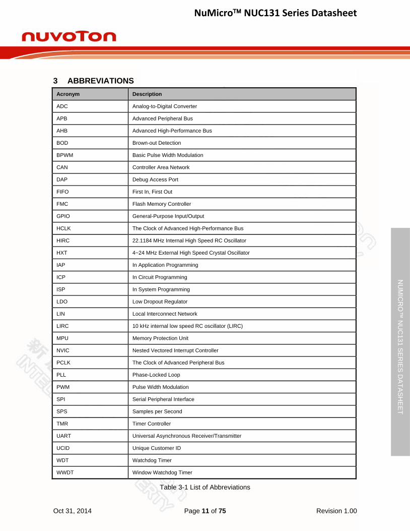
3 ABBREVIATIONS
Acronym Description
ADC Analog-to-Digital Converter
APB Advanced Peripheral Bus
AHB Advanced High-Performance Bus
BOD Brown-out Detection
BPWM Basic Pulse Width Modulation
CAN Controller Area Network
DAP Debug Access Port
FIFO First In, First Out
FMC Flash Memory Controller
GPIO General-Purpose Input/Output
HCLK The Clock of Advanced High-Performance Bus
HIRC 22.1184 MHz Internal High Speed RC Oscillator
HXT 4~24 MHz External High Speed Crystal Oscillator
IAP In Application Programming
ICP In Circuit Programming
ISP In System Programming
LDO Low Dropout Regulator
LIN Local Interconnect Network
LIRC 10 kHz internal low speed RC oscillator (LIRC)
MPU Memory Protection Unit
NVIC Nested Vectored Interrupt Controller
PCLK The Clock of Advanced Peripheral Bus
PLL Phase-Locked Loop
PWM Pulse Width Modulation
SPI Serial Peripheral Interface
SPS Samples per Second
TMR Timer Controller
UART Universal Asynchronous Receiver/Transmitter
UCID Unique Customer ID
WDT Watchdog Timer
WWDT Window Watchdog Timer
Table 3-1 List of Abbreviations

NuMicro NUC131 Series Datasheet
Oct 31, 2014 Page 12 of 75 Revision 1.00
NU
MIC
RO
™ N
UC
13
1 S
ER
IES
DA
TA
SH
EE
T
4 PARTS INFORMATION LIST AND PIN CONFIGURATION
4.1 NuMicro MUC131 Series Selection Code
CPU core
ARM Cortex M0
Package Type
L: LQFP 48 (7x7)
Flash ROM
C: 36 KB Flash ROM
D: 68 KB Flash ROM
Temperature
E: - 40 ~ +105
Version
A: Version
NUC131 - X X E
S: LQFP 64 (7x7)
X X
SRAM Size
2: 8KB SRAM
Figure 4-1 NuMicro NUC131 Series Selection Code

NuMicro NUC131 Series Datasheet
Oct 31, 2014 Page 13 of 75 Revision 1.00
NU
MIC
RO
™ N
UC
13
1 S
ER
IES
DA
TA
SH
EE
T
4.2 NuMicro NUC131 Series Selection Guide P
art
Nu
mb
er
AP
RO
M (
KB
)
RA
M (
KB
)
Data
Fla
sh
(K
B)
ISP
R
OM
(K
B)
I/O
Tim
er
(32
-Bit
)
Connectivity
PW
M (
16
-Bit
)
AD
C (
12
-Bit
)
ISP
/IC
P/I
AP
Pack
ag
e
UA
RT
SP
I
I2C
LIN
CA
N
NUC131LC2AE 36 8 Configurable 4 42 4 6 1 2 3 1 24 8 ch √ LQFP48
NUC131LD2AE 68 8 Configurable 4 42 4 6 1 2 3 1 24 8 ch √ LQFP48
NUC131SC2AE 36 8 Configurable 4 56 4 6 1 2 3 1 24 8 ch √ LQFP64
NUC131SD2AE 68 8 Configurable 4 56 4 6 1 2 3 1 24 8 ch √ LQFP64

NuMicro NUC131 Series Datasheet
Oct 31, 2014 Page 14 of 75 Revision 1.00
NU
MIC
RO
™ N
UC
13
1 S
ER
IES
DA
TA
SH
EE
T
4.3 Pin Configuration
4.3.1 NuMicro NUC131 Pin Diagram
4.3.1.1 NuMicro NUC131SxxAE LQFP 64 pin (7 mm * 7mm)
UART3_RXD/ADC_CH5/PA.5
UART3_TXD/ADC_CH6/PA.6
INT
0/P
B.1
4
PB
.13
BP
WM
1_
CH
3/C
LK
O/P
B.1
2
PW
M1
_C
H4
/I2
C0
_S
DA
/PF
.4
PW
M1
_C
H5
/I2
C0
_S
CL
/PF
.5
PW
M1
_C
H3
/I2
C1
_S
CL
/PA
.11
PW
M1
_C
H2
/I2
C1
_S
DA
/PA
.10
UA
RT
1_
nC
TS
/I2
C0
_S
CL
/PA
.9
UA
RT
1_
nR
TS
/I2
C0
_S
DA
/PA
.8
UA
RT
1_
RX
D/P
B.4
UA
RT
1_
TX
D/P
B.5
UA
RT
1_
nR
TS
/PB
.6
UA
RT
1_
nC
TS
/PB
.7
LD
O_
CA
P
VD
D
VS
S
PWM0_BRAKE1/I2C0_SCL/UART4_RXD/PC.7
PWM0_BRAKE0/I2C0_SDA/UART4_TXD/PC.6
PC.15
PC.14
nRESET
BPWM1_CH2/CLKO/TM0/STADC/PB.8
PA
.4/A
DC
_C
H4
PA
.3/A
DC
_C
H3
/PW
M1
_C
H1
/UA
RT
3_
RX
D
PA
.2/A
DC
_C
H2
/PW
M1
_C
H0
/UA
RT
3_
TX
D
PA
.1/A
DC
_C
H1
/PW
M0
_C
H5
/I2
C1
_S
DA
/UA
RT
5_
RX
D
PA
.0/A
DC
_C
H0
/PW
M0
_C
H4
/I2
C1
_S
CL/U
AR
T5
_T
XD
AV
SS
PA
.12
/PW
M0
_C
H0
/UA
RT
5_
RX
D
PA
.13
/PW
M0
_C
H1
/UA
RT
5_
TX
D
PA
.14
/PW
M0
_C
H2
PA
.15
/PW
M0
_C
H3
PC
.8/P
WM
0_
BR
AK
E0
PC
.9/P
WM
0_
BR
AK
E1
AVDD
VSS
VDD
PC.0/SPI0_SS0/BPWM0_CH0
PC.1/SPI0_CLK/BPWM0_CH1
PC.2/SPI0_MISO0/BPWM0_CH2
PC.3/SPI0_MOSI0/BPWM0_CH3
PD.15/UART2_TXD/BPWM0_CH4
PD.14/UART2_RXD/BPWM0_CH5
PD.7/CAN0_TXD/BPWM1_CH0
PD.6/CAN0_RXD/BPWM1_CH1
PB.3/UART0_nCTS/TM3_EXT/TM3/PWM1_BRAKE0
PB.2/UART0_nRTS/TM2_EXT/TM2/PWM1_BRAKE1
PB.1/UART0_TXD
PB.0/UART0_RXD17
18
19
20
21
22
23
24
25
26
27
28
29
30
31
32
64
63
62
61
60
59
58
57
56
55
54
53
52
51
50
49
16
15
14
13
12
11
10
987654321
33
34
35
36
37
38
39
40
41
42
43
44
45
46
47
48
PC
.10
/PW
M1
_B
RA
KE
0
PC
.11
/PW
M1
_B
RA
KE
1
PB.9/TM1
PB.10/TM2
PB.11/TM3/PWM0_CH4
PE.5/TM1_EXT/TM1/PWM0_CH5
VREF/ADC_CH7/PA.7
PF
.6/IC
E_
CL
K
PF
.7/IC
E_
DA
T
NUC131SxxAE
LQFP 64-pin
BPWM1_CH4/CLKO/PF.8
XT1_OUT/PF.0
BPWM1_CH5/TM0/TM0_EXT/INT1/PB.15
XT1_IN/PF.1
Figure 4-2 NuMicro NUC131SxxAE LQFP 64-pin Diagram

NuMicro NUC131 Series Datasheet
Oct 31, 2014 Page 15 of 75 Revision 1.00
NU
MIC
RO
™ N
UC
13
1 S
ER
IES
DA
TA
SH
EE
T
4.3.1.2 NuMicro NUC131LxxAE LQFP 48 pin
UART3_RXD/ADC_CH5/PA.5
UART3_TXD/ADC_CH6/PA.6
VREF/ADC_CH7/PA.7
BP
WM
1_
CH
3/C
LK
O/P
B.1
2
PW
M1
_C
H4
/I2
C0
_S
DA
/PF
.4
PW
M1
_C
H5
/I2
C0
_S
CL
/PF
.5
PW
M1_
CH
3/I
2C
1_
SC
L/P
A.1
1
PW
M1
_C
H2
/I2
C1
_S
DA
/PA
.10
UA
RT
1_
nC
TS
/I2
C0
_S
CL/P
A.9
UA
RT
1_
nR
TS
/I2
C0
_S
DA
/PA
.8
UA
RT
1_
RX
D/P
B.4
UA
RT
1_
TX
D/P
B.5
LD
O_
CA
P
VD
D
VS
S
PWM0_BRAKE1/I2C0_SCL/UART4_RXD/PC.7
PWM0_BRAKE0/I2C0_SDA/UART4_TXD/PC.6
nRESET
BPWM1_CH2/CLKO/TM0/STADC/PB.8
PA
.4/A
DC
_C
H4
PA
.3/A
DC
_C
H3
/PW
M1
_C
H1
/UA
RT
3_
RX
D
PA
.2/A
DC
_C
H2
/PW
M1
_C
H0
/UA
RT
3_
TX
D
PA
.1/A
DC
_C
H1
/PW
M0
_C
H5
/I2
C1
_S
DA
/UA
RT
5_
RX
D
PA
.0/A
DC
_C
H0
/PW
M0
_C
H4
/I2
C1
_S
CL
/UA
RT
5_
TX
D
AV
SS
PA
.12/P
WM
0_
CH
0/U
AR
T5
_R
XD
PA
.13/P
WM
0_
CH
1/U
AR
T5
_T
XD
PA
.14/P
WM
0_
CH
2
PA
.15/P
WM
0_
CH
3
AVDD
PC.0/SPI0_SS0/BPWM0_CH0
PC.1/SPI0_CLK/BPWM0_CH1
PC.2/SPI0_MISO0/BPWM0_CH2
PC.3/SPI0_MOSI0/BPWM0_CH3
PD.7/CAN0_TXD/BPWM1_CH0
PD.6/CAN0_RXD/BPWM1_CH1
PB.3/UART0_nCTS/TM3_EXT/TM3/PWM1_BRAKE0
PB.2/UART0_nRTS/TM2_EXT/TM2/PWM1_BRAKE1
13
14
15
16
17
18
19
20
21
22
23
24
48
47
46
45
44
43
42
41
40
39
38
37
12
11
10
987654321
25
26
27
28
29
30
31
32
33
34
35
36
NUC131LxxAE
LQFP 48-pin
PD.15/UART2_TXD/BPWM0_CH4
PD.14/UART2_RXD/BPWM0_CH5
PB.1/UART0_TXD
PB.0/UART0_RXD
PF
.6/IC
E_
CL
K
PF
.7/IC
E_
DA
T
BPWM1_CH4/CLKO/PF.8
XT1_OUT/PF.0
BPWM1_CH5/TM0/TM0_EXT/INT1/PB.15
XT1_IN/PF.1
Figure 4-3 NuMicro NUC131LxxAE LQFP 48-pin Diagram

NuMicro NUC131 Series Datasheet
Oct 31, 2014 Page 16 of 75 Revision 1.00
NU
MIC
RO
™ N
UC
13
1 S
ER
IES
DA
TA
SH
EE
T
4.4 Pin Description
4.4.1 NuMicro NUC131 Pin Description
Pin No.
Pin Name Pin
Type Description
LQFP 64-pin
LQFP 48-pin
1 PB.14 I/O General purpose digital I/O pin.
INT0 I External interrupt0 input pin.
2 PB.13 I/O General purpose digital I/O pin.
3 1
PB.12 I/O General purpose digital I/O pin.
CLKO O Frequency divider clock output pin.
BPWM1_CH3 I/O BPWM1 CH3 output/Capture input.
4 2
PF.5 I/O General purpose digital I/O pin.
I2C0_SCL I/O I2C0 clock pin.
PWM1_CH5 I/O PWM1 CH5 output/Capture input.
5 3
PF.4 I/O General purpose digital I/O pin.
I2C0_SDA I/O I2C0 data input/output pin.
PWM1_CH4 I/O PWM1 CH4 output/Capture input.
6 4
PA.11 I/O General purpose digital I/O pin.
I2C1_SCL I/O I2C1 clock pin.
PWM1_CH3 I/O PWM1 CH3 output/Capture input.
7 5
PA.10 I/O General purpose digital I/O pin.
I2C1_SDA I/O I2C1 data input/output pin.
PWM1_CH2 I/O PWM1 CH2 output/Capture input.
8 6
PA.9 I/O General purpose digital I/O pin.
I2C0_SCL I/O I2C0 clock pin.
UART1_nCTS I Clear to Send input pin for UART1.
9 7
PA.8 I/O General purpose digital I/O pin.
I2C0_SDA I/O I2C0 data input/output pin.
UART1_nRTS O Request to Send output pin for UART1.
10 8 PB.4 I/O General purpose digital I/O pin.
UART1_RXD I Data receiver input pin for UART1.
11 9 PB.5 I/O General purpose digital I/O pin.
UART1_TXD O Data transmitter output pin for UART1.
12 PB.6 I/O General purpose digital I/O pin.

NuMicro NUC131 Series Datasheet
Oct 31, 2014 Page 17 of 75 Revision 1.00
NU
MIC
RO
™ N
UC
13
1 S
ER
IES
DA
TA
SH
EE
T
Pin No.
Pin Name Pin
Type Description
LQFP 64-pin
LQFP 48-pin
UART1_nRTS O Request to Send output pin for UART1.
13 PB.7 I/O General purpose digital I/O pin.
UART1_nCTS I Clear to Send input pin for UART1.
14 10 LDO_CAP P LDO output pin.
15 11 VDD P Power supply for I/O ports and LDO source for internal PLL and digital circuit.
16 12 VSS P Ground pin for digital circuit.
17 13 PB.0 I/O General purpose digital I/O pin.
UART0_RXD I Data receiver input pin for UART0.
18 14 PB.1 I/O General purpose digital I/O pin.
UART0_TXD O Data transmitter output pin for UART0.
19 15
PB.2 I/O General purpose digital I/O pin.
UART0_nRTS O Request to Send output pin for UART0.
TM2_EXT I Timer2 external capture input pin.
TM2 O Timer2 toggle output pin.
PWM1_BRAKE1 I PWM1 brake input pin.
20 16
PB.3 I/O General purpose digital I/O pin.
UART0_nCTS I Clear to Send input pin for UART0.
TM3_EXT I Timer3 external capture input pin.
TM3 O Timer3 toggle output pin.
PWM1_BRAKE0 I PWM1 brake input pin.
21 17
PD.6 I/O General purpose digital I/O pin.
CAN0_RXD I Data receiver input pin for CAN0.
BPWM1_CH1 I/O BPWM1 CH1 output/Capture input.
22 18
PD.7 I/O General purpose digital I/O pin.
CAN0_TXD O Data transmitter output pin for CAN0.
BPWM1_CH0 I/O BPWM1 CH0 output/Capture input.
23 19
PD.14 I/O General purpose digital I/O pin.
UART2_RXD I Data receiver input pin for UART2.
BPWM0_CH5 I/O BPWM0 CH5 output/Capture input.
24 20 PD.15 I/O General purpose digital I/O pin.
UART2_TXD O Data transmitter output pin for UART2.

NuMicro NUC131 Series Datasheet
Oct 31, 2014 Page 18 of 75 Revision 1.00
NU
MIC
RO
™ N
UC
13
1 S
ER
IES
DA
TA
SH
EE
T
Pin No.
Pin Name Pin
Type Description
LQFP 64-pin
LQFP 48-pin
BPWM0_CH4 I/O BPWM0 CH4 input/Capture input.
25 21
PC.3 I/O General purpose digital I/O pin.
SPI0_MOSI0 I/O SPI0 MOSI (Master Out, Slave In) pin.
BPWM0_CH3 O BPWM0 CH3 input/Capture input.
26 22
PC.2 I/O General purpose digital I/O pin.
SPI0_MISO0 I/O SPI0 MISO (Master In, Slave Out) pin.
BPWM0_CH2 I BPWM0 CH2 input/Capture input.
27 23
PC.1 I/O General purpose digital I/O pin.
SPI0_CLK I/O SPI0 serial clock pin.
BPWM0_CH1 I/O BPWM0 CH1 input/Capture input.
28 24
PC.0 I/O General purpose digital I/O pin.
SPI0_SS0 I/O SPI0 slave select pin.
BPWM0_CH0 I/O BPWM0 CH0 input/Capture input.
29
PE.5 I/O General purpose digital I/O pin.
PWM0_CH5 I/O PWM0 CH5 output/Capture input.
TM1_EXT I Timer1 external capture input pin.
TM1 O Timer1 toggle output pin.
30
PB.11 I/O General purpose digital I/O pin.
TM3 I/O Timer3 event counter input / toggle output.
PWM0_CH4 I/O PWM0 CH4 output/Capture input.
31 PB.10 I/O General purpose digital I/O pin.
TM2 I/O Timer2 event counter input / toggle output.
32 PB.9 I/O General purpose digital I/O pin.
TM1 I/O Timer1 event counter input / toggle output.
33 PC.11 I/O General purpose digital I/O pin.
PWM1_BRAKE1 I PWM1 brake input pin.
34 PC.10 I/O General purpose digital I/O pin.
PWM1_BRAKE0 I PWM1 brake input pin.
35 PC.9 I/O General purpose digital I/O pin.
PWM0_BRAKE1 I PWM0 brake input pin.
36 PC.8 I/O General purpose digital I/O pin.

NuMicro NUC131 Series Datasheet
Oct 31, 2014 Page 19 of 75 Revision 1.00
NU
MIC
RO
™ N
UC
13
1 S
ER
IES
DA
TA
SH
EE
T
Pin No.
Pin Name Pin
Type Description
LQFP 64-pin
LQFP 48-pin
PWM0_BRAKE0 I PWM0 brake input pin.
37 25 PA.15 I/O General purpose digital I/O pin.
PWM0_CH3 I/O PWM0 CH3 output/Capture input.
38 26 PA.14 I/O General purpose digital I/O pin.
PWM0_CH2 I/O PWM0 CH2 output/Capture input.
39 27
PA.13 I/O General purpose digital I/O pin.
PWM0_CH1 I/O PWM0 CH1 output/Capture input.
UART5_TXD O Data transmitter output pin for UART5.
40 28
PA.12 I/O General purpose digital I/O pin.
PWM0_CH0 I/O PWM0 CH0 output/Capture input.
UART5_RXD I Data receiver input pin for UART5.
41 29 PF.7 I/O General purpose digital I/O pin.
ICE_DAT I/O Serial wire debugger data pin.
42 30 PF.6 I/O General purpose digital I/O pin.
ICE_CLK I Serial wire debugger clock pin.
43 31 AVSS AP Ground pin for analog circuit.
44 32
PA.0 I/O General purpose digital I/O pin.
ADC_CH0 AI ADC_CH0 analog input.
PWM0_CH4 I/O PWM0 CH4 output/Capture input.
I2C1_SCL I/O I2C1 clock pin.
UART5_TXD O Data transmitter output pin for UART5.
45 33
PA.1 I/O General purpose digital I/O pin.
ADC_CH1 AI ADC_CH1 analog input.
PWM0_CH5 I/O PWM0 CH5 output/Capture input.
I2C1_SDA I/O I2C1 data input/output pin.
UART5_RXD I Data receiver input pin for UART5.
46 34
PA.2 I/O General purpose digital I/O pin.
ADC_CH2 AI ADC_CH2 analog input.
PWM1_CH0 I/O PWM1 CH0 output/Capture input.
UART3_TXD O Data transmitter output pin for UART3.
47 35 PA.3 I/O General purpose digital I/O pin.
ADC_CH3 AI ADC_CH3 analog input.

NuMicro NUC131 Series Datasheet
Oct 31, 2014 Page 20 of 75 Revision 1.00
NU
MIC
RO
™ N
UC
13
1 S
ER
IES
DA
TA
SH
EE
T
Pin No.
Pin Name Pin
Type Description
LQFP 64-pin
LQFP 48-pin
PWM1_CH1 I/O PWM1 CH1 output/Capture input.
UART3_RXD I Data receiver input pin for UART3.
48 36 PA.4 I/O General purpose digital I/O pin.
ADC_CH4 AI ADC_CH4 analog input.
49 37
PA.5 I/O General purpose digital I/O pin.
ADC_CH5 AI ADC_CH5 analog input.
UART3_RXD I Data receiver input pin for UART3.
50 38
PA.6 I/O General purpose digital I/O pin.
ADC_CH6 AI ADC_CH6 analog input.
UART3_TXD O Data transmitter output pin for UART3.
51 39
PA.7 I/O General purpose digital I/O pin.
ADC_CH7 AI ADC_CH7 analog input.
VREF AP Voltage reference input for ADC.
52 40 AVDD AP Power supply for internal analog circuit.
53 41
PC.7 I/O General purpose digital I/O pin.
UART4_RXD I Data reveiver input pin for UART4.
I2C0_SCL I/O I2C0 clock pin.
PWM0_BRAKE1 I PWM0 brake input pin.
54 42
PC.6 I/O General purpose digital I/O pin.
UART4_TXD O Data transmitter output pin for UART4.
I2C0_SDA I/O I2C0 data input/output pin.
PWM0_BRAKE0 I PWM0 brake input pin.
55 PC.15 I/O General purpose digital I/O pin.
56 PC.14 I/O General purpose digital I/O pin.
57 43
PB.15 I/O General purpose digital I/O pin.
INT1 I External interrupt1 input pin.
TM0_EXT I Timer0 external capture input pin.
TM0 O Timer0 toggle output pin.
BPWM1_CH5 I/O BPWM1 CH5 output/Capture input.
58 44 PF.0 I/O General purpose digital I/O pin.
XT1_OUT O External 4~24 MHz (high speed) crystal output pin.
59 45 PF.1 I/O General purpose digital I/O pin.

NuMicro NUC131 Series Datasheet
Oct 31, 2014 Page 21 of 75 Revision 1.00
NU
MIC
RO
™ N
UC
13
1 S
ER
IES
DA
TA
SH
EE
T
Pin No.
Pin Name Pin
Type Description
LQFP 64-pin
LQFP 48-pin
XT1_IN I External 4~24 MHz (high speed) crystal input pin.
60 46 nRESET I External reset input: active LOW, with an internal pull-up. Set this pin low reset chip to initial state.
61 VSS P Ground pin for digital circuit.
62 VDD P Power supply for I/O ports and LDO source for internal PLL and digital circuit.
63 47
PF.8 I/O General purpose digital I/O pin.
CLKO O Frequency divider clock output pin.
BPWM1_CH4 I/O BPWM1 CH4 output/Capture input.
64 48
PB.8 I/O General purpose digital I/O pin.
STADC I ADC external trigger input.
TM0 I/O Timer0 event counter input / toggle output.
CLKO O Frequency divider clock output pin.
BPWM1_CH2 I/O BPWM1 CH2 output/Capture input.
Note: Pin Type I = Digital Input, O = Digital Output; AI = Analog Input; P = Power Pin; AP = Analog Power

NuMicro NUC131 Series Datasheet
Oct 31, 2014 Page 22 of 75 Revision 1.00
NU
MIC
RO
™ N
UC
13
1 S
ER
IES
DA
TA
SH
EE
T
5 BLOCK DIAGRAM
5.1 NuMicro NUC131 Block Diagram
Bridge
32-bit Timer X 4
Watchdog Timers X 2
16-bit PWM 24
Channels
Timer / PWM Analog Interface
12-bit ADC X 8-ch
with VREF
APROM 36/68 KB
LDROM 4 KB
Configurable
Data Flash
SRAM 8KB
Memory
ARM
CortexTM –M0
50 MHz
Clock Control
High Speed
Oscillator
22.1184 MHz
Low Speed Oscillator 10 kHz
High Speed External
Crystal Oscillator 4~24 MHz
PLL
GPIO
General Purpose I/O
External Interrupt
Power Control Connectivity
UART X 6
SPI X 1
I²C X 2
CAN X 1
AHB Bus APB Bus
LDO
1.8V
Power On Reset
LVR
Brownout Detection
VREF
Figure 5-1 NuMicro NUC131 Block Diagram

NuMicro NUC131 Series Datasheet
Oct 31, 2014 Page 23 of 75 Revision 1.00
NU
MIC
RO
™ N
UC
13
1 S
ER
IES
DA
TA
SH
EE
T
6 FUNCTIONAL DESCRIPTION
6.1 ARM® Cortex™-M0 Core
The Cortex™-M0 processor is a configurable, multistage, 32-bit RISC processor, which has an AMBA AHB-Lite interface and includes an NVIC component. It also has optional hardware debug functionality. The processor can execute Thumb code and is compatible with other Cortex™-M profile processor. The profile supports two modes -Thread mode and Handler mode. Handler mode is entered as a result of an exception. An exception return can only be issued in Handler mode. Thread mode is entered on Reset, and can be entered as a result of an exception return.
Figure 6-1 shows the functional controller of processor.
CortexTM
-M0
Processor
Core
Nested
Vectored
Interrupt
Controller
(NVIC)
Breakpoint
and
Watchpoint
Unit
Debugger
InterfaceBus Matrix
Debug
Access
Port
(DAP)
DebugCortexTM
-M0 processor
CortexTM
-M0 Components
Wakeup
Interrupt
Controller
(WIC)
Interrupts
Serial Wire or
JTAG Debug Port
AHB-Lite
Interface
Figure 6-1 Functional Controller Diagram
The implemented device provides the following components and features:
A low gate count processor:
- ARMv6-M Thumb® instruction set
- Thumb-2 technology
- ARMv6-M compliant 24-bit SysTick timer
- A 32-bit hardware multiplier
- System interface supported with little-endian data accesses
- Ability to have deterministic, fixed-latency, interrupt handling
- Load/store-multiples and multicycle-multiplies that can be abandoned and restarted to facilitate rapid interrupt handling
- C Application Binary Interface compliant exception model. This is the ARMv6-M, C Application Binary Interface (C-ABI) compliant exception model that enables the use of pure C functions as interrupt handlers
- Low Power Sleep mode entry using Wait For Interrupt (WFI), Wait For Event

NuMicro NUC131 Series Datasheet
Oct 31, 2014 Page 24 of 75 Revision 1.00
NU
MIC
RO
™ N
UC
13
1 S
ER
IES
DA
TA
SH
EE
T
(WFE) instructions, or the return from interrupt sleep-on-exit feature
NVIC:
- 32 external interrupt inputs, each with four levels of priority
- Dedicated Non-maskable Interrupt (NMI) input
- Supports for both level-sensitive and pulse-sensitive interrupt lines
- Supports Wake-up Interrupt Controller (WIC) and, providing Ultra-low Power Sleep mode
Debug support
- Four hardware breakpoints
- Two watchpoints
- Program Counter Sampling Register (PCSR) for non-intrusive code profiling
- Single step and vector catch capabilities
Bus interfaces:
- Single 32-bit AMBA-3 AHB-Lite system interface that provides simple integration to all system peripherals and memory
- Single 32-bit slave port that supports the DAP (Debug Access Port)
NuMicro NUC131 Series Datasheet
Oct 31, 2014 Page 25 of 75 Revision 1.00
NU
MIC
RO
™ N
UC
13
1 S
ER
IES
DA
TA
SH
EE
T
6.2 System Manager
6.2.1 Overview
System management includes the following sections:
System Resets
System Memory Map
System management registers for Part Number ID, chip reset and on-chip controllers reset , multi-functional pin control
System Timer (SysTick)
Nested Vectored Interrupt Controller (NVIC)
System Control registers
6.2.2 System Reset
The system reset can be issued by one of the following listed events. For these reset event flags can be read by RSTSRC register.
Power-on Reset
Low level on the nRESET pin
Watchdog Time-out Reset
Low Voltage Reset
Brown-out Detector Reset
CPU Reset
System Reset
System Reset and Power-on Reset all reset the whole chip including all peripherals. The difference between System Reset and Power-on Reset is external crystal circuit and BS (ISPCON[1]) bit. System Reset does not reset external crystal circuit and BS (ISPCON[1]) bit, but Power-on Reset does.
NuMicro NUC131 Series Datasheet
Oct 31, 2014 Page 26 of 75 Revision 1.00
NU
MIC
RO
™ N
UC
13
1 S
ER
IES
DA
TA
SH
EE
T
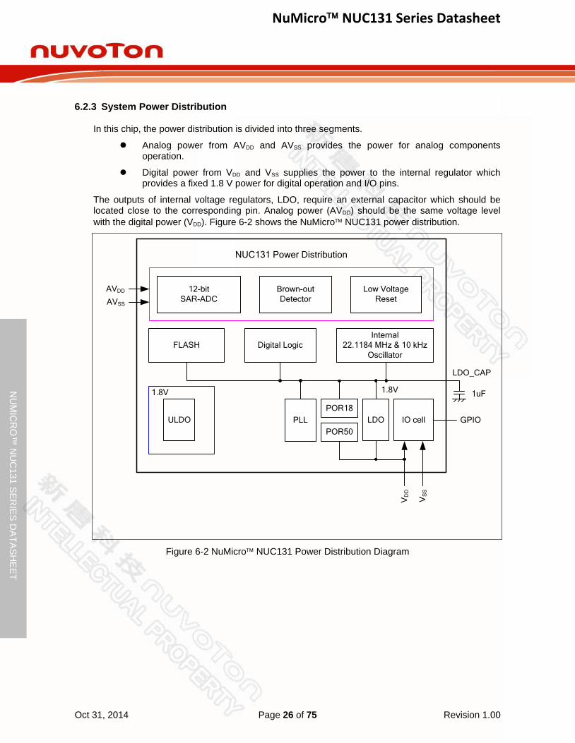
6.2.3 System Power Distribution
In this chip, the power distribution is divided into three segments.
Analog power from AVDD and AVSS provides the power for analog components operation.
Digital power from VDD and VSS supplies the power to the internal regulator which provides a fixed 1.8 V power for digital operation and I/O pins.
The outputs of internal voltage regulators, LDO, require an external capacitor which should be located close to the corresponding pin. Analog power (AVDD) should be the same voltage level
with the digital power (VDD). Figure 6-2 shows the NuMicro NUC131 power distribution.
12-bit
SAR-ADC
Brown-out
Detector
Low Voltage
Reset
FLASH Digital Logic
Internal
22.1184 MHz & 10 kHz
Oscillator
AVDD
AVSS
LDO_CAP
1uF
GPIO
NUC131 Power Distribution
LDOPLL
POR50
POR18 V
DD
VS
SIO cellULDO
1.8V 1.8V
Figure 6-2 NuMicro NUC131 Power Distribution Diagram

NuMicro NUC131 Series Datasheet
Oct 31, 2014 Page 27 of 75 Revision 1.00
NU
MIC
RO
™ N
UC
13
1 S
ER
IES
DA
TA
SH
EE
T
6.2.4 System Memory Map
The NuMicro NUC131 series provides 4G-byte addressing space. The memory locations assigned to each on-chip controllers are shown in the following table. The detailed register definition, memory space, and programming detailed will be described in the following sections for each on-chip
peripheral. The NuMicro NUC131 series only supports little-endian data format.
Address Space Token Controllers
Flash and SRAM Memory Space
0x0000_0000 – 0x0001_0FFF FLASH_BA FLASH Memory Space (68 KB)
0x2000_0000 – 0x2000_3FFF SRAM_BA SRAM Memory Space (8 KB)
AHB Controllers Space (0x5000_0000 – 0x501F_FFFF)
0x5000_0000 – 0x5000_01FF GCR_BA System Global Control Registers
0x5000_0200 – 0x5000_02FF CLK_BA Clock Control Registers
0x5000_0300 – 0x5000_03FF INT_BA Interrupt Multiplexer Control Registers
0x5000_4000 – 0x5000_7FFF GPIO_BA GPIO Control Registers
0x5000_C000 – 0x5000_FFFF FMC_BA Flash Memory Control Registers
APB1 Controllers Space (0x4000_0000 ~ 0x400F_FFFF)
0x4000_4000 – 0x4000_7FFF WDT_BA Watchdog Timer Control Registers
0x4001_0000 – 0x4001_3FFF TMR01_BA Timer0/Timer1 Control Registers
0x4002_0000 – 0x4002_3FFF I2C0_BA I2C0 Interface Control Registers
0x4003_0000 – 0x4003_3FFF SPI0_BA SPI0 with master/slave function Control Registers
0x4004_0000 – 0x4004_3FFF PWM0_BA PWM0 Control Registers
0x4004_4000 – 0x4004_7FFF BPWM0_BA BPWM0 Control Registers
0x4005_0000 – 0x4005_3FFF UART0_BA UART0 Control Registers
0x4005_4000 – 0x4005_7FFF UART3_BA UART3 Control Registers
0x4005_8000 – 0x4005_BFFF UART4_BA UART4 Control Registers
0x400E_0000 – 0x400E_FFFF ADC_BA Analog-Digital-Converter (ADC) Control Registers
APB2 Controllers Space (0x4010_0000 ~ 0x401F_FFFF)
0x4011_0000 – 0x4011_3FFF TMR23_BA Timer2/Timer3 Control Registers
0x4012_0000 – 0x4012_3FFF I2C1_BA I2C1 Interface Control Registers
0x4014_0000 – 0x4014_3FFF PWM1_BA PWM1 Control Registers
0x4014_4000 – 0x4014_7FFF BPWM1_BA BPWM1 Control Registers
0x4015_0000 – 0x4015_3FFF UART1_BA UART1 Control Registers
0x4015_4000 – 0x4015_7FFF UART2_BA UART2 Control Registers
0x4015_8000 – 0x4015_BFFF UART5_BA UART5 Control Registers
0x4018_0000 – 0x4018_3FFF CAN0_BA CAN0 Bus Control Registers

NuMicro NUC131 Series Datasheet
Oct 31, 2014 Page 28 of 75 Revision 1.00
NU
MIC
RO
™ N
UC
13
1 S
ER
IES
DA
TA
SH
EE
T
System Controllers Space (0xE000_E000 ~ 0xE000_EFFF)
0xE000_E010 – 0xE000_E0FF SCS_BA System Timer Control Registers
0xE000_E100 – 0xE000_ECFF SCS_BA External Interrupt Controller Control Registers
0xE000_ED00 – 0xE000_ED8F SCS_BA System Control Registers
Table 6-1 Address Space Assignments for On-Chip Controllers

NuMicro NUC131 Series Datasheet
Oct 31, 2014 Page 29 of 75 Revision 1.00
NU
MIC
RO
™ N
UC
13
1 S
ER
IES
DA
TA
SH
EE
T
6.2.5 System Timer (SysTick)
The Cortex™-M0 includes an integrated system timer, SysTick, which provides a simple, 24-bit clear-on-write, decrementing, wrap-on-zero counter with a flexible control mechanism. The counter can be used as a Real Time Operating System (RTOS) tick timer or as a simple counter.
When system timer is enabled, it will count down from the value in the SysTick Current Value Register (SYST_CVR) to 0, and reload (wrap) to the value in the SysTick Reload Value Register (SYST_RVR) on the next clock cycle, then decrement on subsequent clocks. When the counter transitions to 0, the COUNTFLAG status bit is set. The COUNTFLAG bit clears on reads.
The SYST_CVR value is unknown on reset. Software should write to the register to clear it to 0 before enabling the feature. This ensures the timer will count from the SYST_RVR value rather than an arbitrary value when it is enabled.
If the SYST_RVR is 0, the timer will be maintained with a current value of 0 after it is reloaded with this value. This mechanism can be used to disable the feature independently from the timer enable bit.
For more detailed information, please refer to the “ARM® Cortex™-M0 Technical Reference
Manual” and “ARM® v6-M Architecture Reference Manual”.

NuMicro NUC131 Series Datasheet
Oct 31, 2014 Page 30 of 75 Revision 1.00
NU
MIC
RO
™ N
UC
13
1 S
ER
IES
DA
TA
SH
EE
T
6.2.6 Nested Vectored Interrupt Controller (NVIC)
The Cortex™-M0 provides an interrupt controller as an integral part of the exception mode, named as “Nested Vectored Interrupt Controller (NVIC)”, which is closely coupled to the processor core and provides following features:
Nested and Vectored interrupt support
Automatic processor state saving and restoration
Reduced and deterministic interrupt latency
The NVIC prioritizes and handles all supported exceptions. All exceptions are handled in “Handler Mode”. This NVIC architecture supports 32 (IRQ[31:0]) discrete interrupts with 4 levels of priority. All of the interrupts and most of the system exceptions can be configured to different priority levels. When an interrupt occurs, the NVIC will compare the priority of the new interrupt to the current running one’s priority. If the priority of the new interrupt is higher than the current one, the new interrupt handler will override the current handler.
When an interrupt is accepted, the starting address of the interrupt service routine (ISR) is fetched from a vector table in memory. There is no need to determine which interrupt is accepted and branch to the starting address of the correlated ISR by software. While the starting address is fetched, NVIC will also automatically save processor state including the registers “PC, PSR, LR, R0~R3, R12” to the stack. At the end of the ISR, the NVIC will restore the mentioned registers from stack and resume the normal execution. Thus it will take less and deterministic time to process the interrupt request.
The NVIC supports “Tail Chaining” which handles back-to-back interrupts efficiently without the overhead of states saving and restoration and therefore reduces delay time in switching to pending ISR at the end of current ISR. The NVIC also supports “Late Arrival” which improves the efficiency of concurrent ISRs. When a higher priority interrupt request occurs before the current ISR starts to execute (at the stage of state saving and starting address fetching), the NVIC will give priority to the higher one without delay penalty. Thus it advances the real-time capability.
For more detailed information, please refer to the “ARM® Cortex™-M0 Technical Reference
Manual” and “ARM® v6-M Architecture Reference Manual”.

NuMicro NUC131 Series Datasheet
Oct 31, 2014 Page 31 of 75 Revision 1.00
NU
MIC
RO
™ N
UC
13
1 S
ER
IES
DA
TA
SH
EE
T
6.2.6.1 Exception Model and System Interrupt Map
The following table lists the exception model supported by NuMicro NUC131 series. Software can set four levels of priority on some of these exceptions as well as on all interrupts. The highest user-configurable priority is denoted as “0” and the lowest priority is denoted as “3”. The default priority of all the user-configurable interrupts is “0”. Note that priority “0” is treated as the fourth priority on the system, after three system exceptions “Reset”, “NMI” and “Hard Fault”.
Exception Name Vector Number Priority
Reset 1 -3
NMI 2 -2
Hard Fault 3 -1
Reserved 4 ~ 10 Reserved
SVCall 11 Configurable
Reserved 12 ~ 13 Reserved
PendSV 14 Configurable
SysTick 15 Configurable
Interrupt (IRQ0 ~ IRQ31) 16 ~ 47 Configurable
Table 6-2 Exception Model
Vector Number
Interrupt Number
(Bit In Interrupt Registers)
Interrupt Name Source Module
Interrupt Description
1 ~ 15 - - - System exceptions
16 0 BOD_INT Brown-out Brown-out low voltage detected interrupt
17 1 WDT_INT WDT Watchdog Timer interrupt
18 2 EINT0 GPIO External signal interrupt from PB.14 pin
19 3 EINT1 GPIO External signal interrupt from PB.15 pin
20 4 GPAB_INT GPIO External signal interrupt from PA[15:0]/PB[13:0]
21 5 GPCDEF_INT GPIO External interrupt from PC[15:0]/PD[15:0]/PE[15:0]/PF[8:0]
22 6 - - Reserved
23 7 - - Reserved
24 8 TMR0_INT TMR0 Timer 0 interrupt
25 9 TMR1_INT TMR1 Timer 1 interrupt
26 10 TMR2_INT TMR2 Timer 2 interrupt
27 11 TMR3_INT TMR3 Timer 3 interrupt
28 12 UART02_INT UART0/2 UART0 and UART2 interrupt
29 13 UART1_INT UART1 UART1 interrupt

NuMicro NUC131 Series Datasheet
Oct 31, 2014 Page 32 of 75 Revision 1.00
NU
MIC
RO
™ N
UC
13
1 S
ER
IES
DA
TA
SH
EE
T
30 14 SPI0_INT SPI0 SPI0 interrupt
31 15 UART3_INT UART3 UART3 interrupt
32 16 UART4_INT UART4 UART4 interrupt
33 17 UART5_INT UART5 UART5 interrupt
34 18 I2C0_INT I2C0 I
2C0 interrupt
35 19 I2C1_INT I2C1 I
2C1 interrupt
36 20 CAN0_INT CAN0 CAN0 interrupt
37 21 - - Reserved
38 22 PWM0_INT PWM0 PWM0 interrupt
39 23 PWM1_INT PWM1 PWM1 interrupt
40 24 BPWM0_INT BPWM0 BPWM0 interrupt
41 25 BPWM1_INT BPWM1 BPWM1 interrupt
42 26 BRAKE0_INT PWM0 PWM0 brake interrupt
43 27 BRAKE1_INT PWM1 PWM1 brake interrupt
44 28 PWRWU_INT CLKC Clock controller interrupt for chip wake-up from Power-down state
45 29 ADC_INT ADC ADC interrupt
46 30 CKD_INT CLKC Clock detection interrupt
47 31 - - Reserved
Table 6-3 System Interrupt Map

NuMicro NUC131 Series Datasheet
Oct 31, 2014 Page 33 of 75 Revision 1.00
NU
MIC
RO
™ N
UC
13
1 S
ER
IES
DA
TA
SH
EE
T
6.2.6.2 Vector Table
When an interrupt is accepted, the processor will automatically fetch the starting address of the interrupt service routine (ISR) from a vector table in memory. For ARMv6-M, the vector table base address is fixed at 0x00000000. The vector table contains the initialization value for the stack pointer on reset, and the entry point addresses for all exception handlers. The vector number on previous page defines the order of entries in the vector table associated with exception handler entry as illustrated in previous section.
Vector Table Word Offset Description
0 SP_main – The Main stack pointer
Vector Number Exception Entry Pointer using that Vector Number
Table 6-4 Vector Table Format
6.2.6.3 Operation Description
NVIC interrupts can be enabled and disabled by writing to their corresponding Interrupt Set-Enable or Interrupt Clear-Enable register bit-field. The registers use a write-1-to-enable and write-1-to-clear policy, both registers reading back the current enabled state of the corresponding interrupts. When an interrupt is disabled, interrupt assertion will cause the interrupt to become Pending, however, the interrupt will not activate. If an interrupt is Active when it is disabled, it remains in its Active state until cleared by reset or an exception return. Clearing the enable bit prevents new activations of the associated interrupt.
NVIC interrupts can be pended/un-pended using a complementary pair of registers to those used to enable/disable the interrupts, named the Set-Pending Register and Clear-Pending Register respectively. The registers use a write-1-to-enable and write-1-to-clear policy, both registers reading back the current pended state of the corresponding interrupts. The Clear-Pending Register has no effect on the execution status of an Active interrupt.
NVIC interrupts are prioritized by updating an 8-bit field within a 32-bit register (each register supporting four interrupts).
The general registers associated with the NVIC are all accessible from a block of memory in the System Control Space and will be described in next section.

NuMicro NUC131 Series Datasheet
Oct 31, 2014 Page 34 of 75 Revision 1.00
NU
MIC
RO
™ N
UC
13
1 S
ER
IES
DA
TA
SH
EE
T
6.2.7 System Control
The Cortex™-M0 status and operating mode control are managed by System Control Registers. Including CPUID, Cortex™-M0 interrupt priority and Cortex™-M0 power management can be controlled through these system control registers.
For more detailed information, please refer to the “ARM® Cortex™-M0 Technical Reference
Manual” and “ARM® v6-M Architecture Reference Manual”.

NuMicro NUC131 Series Datasheet
Oct 31, 2014 Page 35 of 75 Revision 1.00
NU
MIC
RO
™ N
UC
13
1 S
ER
IES
DA
TA
SH
EE
T
6.3 Clock Controller
6.3.1 Overview
The clock controller generates the clocks for the whole chip, including system clocks and all peripheral clocks. The clock controller also implements the power control function with the individually clock ON/OFF control, clock source selection and clock divider. The chip enters Power-down mode when Cortex™-M0 core executes the WFI instruction only if the PWR_DOWN_EN (PWRCON[7]) bit and PD_WAIT_CPU (PWRCON[8]) bit are both set to 1. After that, chip enters Power-down mode and wait for wake-up interrupt source triggered to leave Power-down mode. In the Power-down mode, the clock controller turns off the 4~24 MHz external high speed crystal oscillator and 22.1184 MHz internal high speed RC oscillator to reduce the overall system power consumption. The following figures show the clock generator and the overview of the clock source control.
The clock generator consists of 5 clock sources as listed below:
4~24 MHz external high speed crystal oscillator (HXT)
Programmable PLL output clock frequency(PLL FOUT),PLL source can be from external 4~24 MHz external high speed crystal oscillator (HXT) or 22.1184 MHz internal high speed RC oscillator (HIRC))
22.1184 MHz internal high speed RC oscillator (HIRC)
10 kHz internal low speed RC oscillator (LIRC)
XT1_IN
4~24 MHz
HXT
XTL12M_EN (PWRCON[0])
XT1_OUT
22.1184 MHz
HIRC
OSC22M_EN (PWRCON[2])
0
1
PLL
PLL_SRC (PLLCON[19])
PLL FOUT
10 kHz
LIRC
OSC10K_EN (PWRCON[3])
HXT
HIRC
LIRC
Legend:
HXT = 4~24 MHz external high speed crystal oscillator
HIRC = 22.1184 MHz internal high speed RC oscillator
LIRC = 10 kHz internal low speed RC oscillator
Figure 6-3 Clock Generator Block Diagram

NuMicro NUC131 Series Datasheet
Oct 31, 2014 Page 36 of 75 Revision 1.00
NU
MIC
RO
™ N
UC
13
1 S
ER
IES
DA
TA
SH
EE
T
1
0
PLLCON[19]
22.1184
MHz
4~24
MHz
PLLFOUT
111
011
010
001
4~24 MHz
Reserved
4~24 MHz
HCLK
22.1184 MHz
000
1/2
1/2
1/2
CLKSEL0[5:3]
1
0SysTick
TMR 0
ADC
UART 0~5
ISP
WDT
BPWM 0
TMR 3
TMR 2
TMR 1
CPU
FMC
10 kHz
011
010
001
000
HCLK
Reserved
4~24 MHz
111
011
010
001
PLLFOUT
Reserved
4~24 MHz
10 kHz
22.1184 MHz
000
CLKSEL0[2:0]
SYST_CSR[2]
CPUCLK
1/(HCLK_N+1)
PCLK
CPUCLK
HCLK
11
01
00
PLLFOUT
4~24 MHz
HCLK
CLKSEL1[3:2]
External trigger
CLKSEL1[22:20]
CLKSEL1[18:16]
CLKSEL1[14:12]
CLKSEL1[10:8]
22.1184 MHz
WWDT
10 kHz
1/(ADC_N+1)
11
10
CLKSEL1[1:0]
HCLK1/2048
1/(UART_N+1)
22.1184 MHz
4~24 MHz
11
01
00
PLLFOUT
4~24 MHz
22.1184 MHz
CLKSEL1[25:24]
22.1184 MHz
10
10 kHz
22.1184 MHz
101
111
1
0SPI 0
CLKSEL1[4]
HCLK
11
10
01
00
HCLK
4~24 MHz
22.1184 MHz
Reserved
CLKSEL2[3:2]
FDIV
BOD10 kHz
11
10
CLKSEL2[17:16]
10 kHz
CLKSEL3[17]
CLKSEL3[18]
I2C 0~1
PLLFOUT
CAN 0
PWM 01
0
PCLK
PLLFOUT
BPWM 1
PWM 1
CLKSEL3[16]
CLKSEL3[19]HCLK
1/2048
Figure 6-4 Clock Generator Global View Diagram
6.3.2 System Clock and SysTick Clock
The system clock has 4 clock sources which were generated from clock generator block. The
NuMicro NUC131 Series Datasheet
Oct 31, 2014 Page 37 of 75 Revision 1.00
NU
MIC
RO
™ N
UC
13
1 S
ER
IES
DA
TA
SH
EE
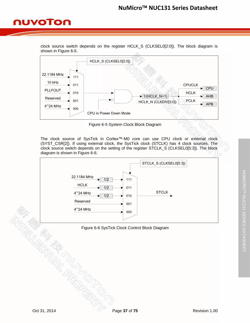
T
clock source switch depends on the register HCLK_S (CLKSEL0[2:0]). The block diagram is shown in Figure 6-5.
111
011
010
001
PLLFOUT
Reserved
4~24 MHz
10 kHz
HCLK_S (CLKSEL0[2:0])
22.1184 MHz
000
1/(HCLK_N+1)
HCLK_N (CLKDIV[3:0])
CPU in Power Down Mode
CPU
AHB
APB
CPUCLK
HCLK
PCLK
Figure 6-5 System Clock Block Diagram
The clock source of SysTick in Cortex™-M0 core can use CPU clock or external clock (SYST_CSR[2]). If using external clock, the SysTick clock (STCLK) has 4 clock sources. The clock source switch depends on the setting of the register STCLK_S (CLKSEL0[5:3]). The block diagram is shown in Figure 6-6.
111
011
010
001
4~24 MHz
Reserved
4~24 MHz
HCLK
STCLK_S (CLKSEL0[5:3])
STCLK
22.1184 MHz
000
1/2
1/2
1/2
Figure 6-6 SysTick Clock Control Block Diagram

NuMicro NUC131 Series Datasheet
Oct 31, 2014 Page 38 of 75 Revision 1.00
NU
MIC
RO
™ N
UC
13
1 S
ER
IES
DA
TA
SH
EE
T
6.3.3 Power-down Mode Clock
When chip enters Power-down mode, system clocks, some clock sources, and some peripheral clocks will be disabled. Some clock sources and peripherals clocks are still active in Power-down mode.
The clocks still kept active are listed below:
Clock Generator
- 10 kHz internal low speed RC oscillator (LIRC) clock
WDT/Timer Peripherals Clock (when 10 kHz intertnal low speed RC oscillator (LIRC) is adopted as clock source)

NuMicro NUC131 Series Datasheet
Oct 31, 2014 Page 39 of 75 Revision 1.00
NU
MIC
RO
™ N
UC
13
1 S
ER
IES
DA
TA
SH
EE
T
6.3.4 Frequency Divider Output
This device is equipped with a power-of-2 frequency divider which is composed by16 chained divide-by-2 shift registers. One of the 16 shift register outputs selected by a sixteen to one multiplexer is reflected to CLKO function pin. Therefore there are 16 options of power-of-2 divided clocks with the frequency from Fin/2
1 to Fin/2
16 where Fin is input clock frequency to the clock
divider.
The output formula is Fout = Fin/2(N+1)
, where Fin is the input clock frequency, Fout is the clock divider output frequency and N is the 4-bit value in FSEL (FRQDIV[3:0]).
When writing 1 to DIVIDER_EN (FRQDIV[4]), the chained counter starts to count. When writing 0 to DIVIDER_EN (FRQDIV[4]), the chained counter continuously runs till divided clock reaches low state and stay in low state.
If DIVIDER1(FRQDIV[5]) is set to 1, the frequency divider clock (FRQDIV_CLK) will bypass power-of-2 frequency divider. The frequency divider clock will be output to CLKO pin directly.
11
10
01
00
HCLK
Reserved
4~24 MHz
22.1184 MHz
FRQDIV_S (CLKSEL2[3:2])
FDIV_EN (APBCLK[6])
FRQDIV_CLK
Figure 6-7 Clock Source of Frequency Divider
0000
0001
1110
1111
:
:
16 to 1
MUX
1/2 1/22 1/23 1/215 1/216…...
FSEL
(FRQDIV[3:0])
CLKO
FRQDIV_CLK
16 chained
divide-by-2 counter
DIVIDER_EN
(FRQDIV[4])Enable
divide-by-2 counter
0
1
DIVIDER1
(FRQDIV[5])
Figure 6-8 Frequency Divider Block Diagram

NuMicro NUC131 Series Datasheet
Oct 31, 2014 Page 40 of 75 Revision 1.00
NU
MIC
RO
™ N
UC
13
1 S
ER
IES
DA
TA
SH
EE
T
6.4 Flash Memory Controller (FMC)
6.4.1 Overview
The NuMicro NUC131 series has 68/36K bytes on-chip embedded Flash for application program memory (APROM) that can be updated through ISP procedure. The In-System-Programming (ISP) function enables user to update program memory when chip is soldered on PCB. After chip is powered on, Cortex™-M0 CPU fetches code from APROM or LDROM decided
by boot select (CBS) in CONFIG0. By the way, the NuMicro NUC131 series also provides additional Data Flash for user to store some application dependent data.
The NuMicro NUC131 supports another flexible feature: configurable Data Flash size. The Data Flash size is decided by Data Flash variable size enable (DFVSEN), Data Flash enable (DFEN) in Config0 and Data Flash base address (DFBADR) in Config1. When DFVSEN is set to 1, the Data Flash size is fixed at 4K and the address is started from 0x0001_f000, and the APROM size is become 64/32K. When DFVSEN is set to 0 and DFEN is set to 1, the Data Flash size is zero and the APROM size is 68/36K bytes. When DFVSEN is set to 0 and DFEN is set to 0, the APROM and Data Flash share 68/36K bytes continuous address and the start address of Data Flash is defined by (DFBADR) in Config1.
6.4.2 Features
Runs up to 50 MHz with zero wait cycle for continuous address read access
All embedded flash memory supports 512 bytes page erase
68/36 KB application program memory (APROM)
4KB In-System-Programming (ISP) loader program memory (LDROM)
Configurable Data Flash size
512 bytes page erase unit
Supports In-Application-Programming (IAP) to switch code between APROM and LDROM without reset
In-System-Programming (ISP) to update on-chip Flash

NuMicro NUC131 Series Datasheet
Oct 31, 2014 Page 41 of 75 Revision 1.00
NU
MIC
RO
™ N
UC
13
1 S
ER
IES
DA
TA
SH
EE
T
6.5 General Purpose I/O (GPIO)
6.5.1 Overview
The NuMicro NUC131 series has up to 56 General Purpose I/O pins to be shared with other function pins depending on the chip configuration. These 56 pins are arranged in 6 ports named as GPIOA, GPIOB, GPIOC, GPIOD, GPIOE and GPIOF. The GPIOA/B port has the maximum of 16 pins. The GPIOC port has the maximum of 12 pins. The GPIOD port has the maximum of 4 pins. The GPIOE port has the maximum of 1 pin. The GPIOF port has the maximum of 7 pins. Each of the 56 pins is independent and has the corresponding register bits to control the pin mode function and data.
The I/O type of each of I/O pins can be configured by software individually as input, output, open-drain or Quasi-bidirectional mode. After reset, the I/O mode of all pins are depending on Config0[10] setting. In Quasi-bidirectional mode, I/O pin has a very weak individual pull-up
resistor which is about 110~300 K for VDD from 5.0 V to 2.5 V.
6.5.2 Features
Four I/O modes:
- Quasi-bidirectional
- Push-Pull output
- Open-Drain output
- Input only with high impendence
TTL/Schmitt trigger input selectable by GPx_TYPE[15:0] in GPx_MFP[31:16]
I/O pin configured as interrupt source with edge/level setting
Configurable default I/O mode of all pins after reset by Config0[10] setting
- If Config[10] is 0, all GPIO pins in input tri-state mode after chip reset
- If Config[10] is 1, all GPIO pins in Quasi-bidirectional mode after chip reset
I/O pin internal pull-up resistor enabled only in Quasi-bidirectional I/O mode
Enabling the pin interrupt function will also enable the pin wake-up function

NuMicro NUC131 Series Datasheet
Oct 31, 2014 Page 42 of 75 Revision 1.00
NU
MIC
RO
™ N
UC
13
1 S
ER
IES
DA
TA
SH
EE
T
6.6 Timer Controller (TIMER)
6.6.1 Overview
The timer controller includes four 32-bit timers, TIMER0 ~ TIMER3, allowing user to easily implement a timer control for applications. The timer can perform functions, such as frequency measurement, delay timing, clock generation, and event counting by external input pins, and interval measurement by external capture pins.
6.6.2 Features
Four sets of 32-bit timers with 24-bit up counter and one 8-bit prescale counter
Independent clock source for each timer
Provides four timer counting modes: one-shot, periodic, toggle and continuous counting
Time-out period = (Period of timer clock input) * (8-bit prescale counter + 1) * (24-bit TCMP)
Maximum counting cycle time = (1 / T MHz) * (28) * (2
24), T is the period of timer clock
24-bit up counter value is readable through TDR (Timer Data Register)
Supports event counting function to count the event from external counter pin (TM0~TM3)
Supports external pin capture (TM0_EXT~TM3_EXT) for interval measurement
Supports external pin capture (TM0_EXT~TM3_EXT) for reset 24-bit up counter
Supports chip wake-up from Idle/Power-down mode if a timer interrupt signal is generated

NuMicro NUC131 Series Datasheet
Oct 31, 2014 Page 43 of 75 Revision 1.00
NU
MIC
RO
™ N
UC
13
1 S
ER
IES
DA
TA
SH
EE
T
6.7 PWM Generator and Capture Timer (PWM)
6.7.1 Overview
The NUC131 provides two PWM generators - PWM0 and PWM1. Each PWM supports 6
channels of PWM output or input capture. There is a 12-bit prescaler to support flexible clock to the 16-bit PWM counter with 16-bit comparator. The PWM counter supports up, down and up-down counter types. PWM uses the comparator compared with counter to generate events. These events are used to generate PWM pulse, interrupt and trigger signal for ADC to start conversion.
The PWM generator supports two standard PWM output modes: Independent mode and Complementary mode, which have difference architecture. In Complementary mode, there are two comparators to generate various PWM pulse with 12-bit dead-time generator. For PWM output control unit, it supports polarity output, independent pin mask, tri-state output enable and brake functions.
The PWM generator also supports input capture function to latch PWM counter value to the corresponding register when input channel has a rising transition, falling transition or both transition is happened.
6.7.2 Features
6.7.2.1 PWM function features
Supports maximum clock frequency up to100 MHz
Supports up to two PWM modules, each module provides 6 output channels
Supports independent mode for PWM output/Capture input channel
Supports complementary mode for 3 complementary paired PWM output channel
Dead-time insertion with 12-bit resolution
Two compared values during one period
Supports 12-bit pre-scalar from 1 to 4096
Supports 16-bit resolution PWM counter, each module provides 3 PWM counters
Up, down and up/down counter operation type
Supports mask function and tri-state enable for each PWM pin
Supports brake function
Brake source from pin and system safety events (clock failed, Brown-out detection and CPU lockup)
Noise filter for brake source from pin
Edge detect brake source to control brake state until brake interrupt cleared
Level detect brake source to auto recover function after brake condition removed
Supports interrupt on the following events:
PWM counter match zero, period value or compared value
Brake condition happened
Supports trigger ADC on the following events:

NuMicro NUC131 Series Datasheet
Oct 31, 2014 Page 44 of 75 Revision 1.00
NU
MIC
RO
™ N
UC
13
1 S
ER
IES
DA
TA
SH
EE
T
PWM counter match zero, period value or compared value
6.7.2.2 Capture Function Features
Supports up to 12 capture input channels with 16-bit resolution
Supports rising or falling capture condition
Supports input rising/falling capture interrupt
Supports rising/falling capture with counter reload option
6.7.2.3 Compare table
Feature PWM BPWM
Counter number 2 channels share 1 timer, total 6
timers 6 channels share 1 timer, total 1
timer
Complementary mode V X
Dead-time function V X
Brake function V X
Capture reload 2 channels reload 1 timer 6 channels reload 1 timer
Table 6-5 PWM and BPWM Features Different Table

NuMicro NUC131 Series Datasheet
Oct 31, 2014 Page 45 of 75 Revision 1.00
NU
MIC
RO
™ N
UC
13
1 S
ER
IES
DA
TA
SH
EE
T
6.8 Basic PWM Generator and Capture Timer (BPWM)
6.8.1 Overview
The NUC131 provides two BPWM generators - BPWM0 and BPWM1. Each BPWM supports 6
channels of BPWM output or input capture. There is a 12-bit prescaler to support flexible clock to the 16-bit BPWM counter with 16-bit comparator. The BPWM counter supports up, down and up-down counter types, all 6 channels share one counter. BPWM uses the comparator compared with counter to generate events. These events are used to generate BPWM pulse, interrupt and trigger signal for ADC to start conversion. For BPWM output control unit, it supports polarity output, independent pin mask and tri-state output enable.
The BPWM generator also supports input capture function to latch BPWM counter value to corresponding register when input channel has a rising transition, falling transition or both transition is happened.
6.8.2 Features
6.8.2.1 BPWM function features
Supports maximum clock frequency up to100 MHz
Supports up to two BPWM modules, each module provides 6 output channels
Supports independent mode for BPWM output/Capture input channel
Supports 12-bit pre-scalar from 1 to 4096
Supports 16-bit resolution BPWM counter, each module provides 1 BPWM counter
Up, down and up/down counter operation type
Supports mask function and tri-state enable for each BPWM pin
Supports interrupt on the following events:
BPWM counter match zero, period value or compared value
Supports trigger ADC on the following events:
BPWM counter match zero, period value or compared value
6.8.2.2 Capture Function Features
Supports up to 12 capture input channels with 16-bit resolution
Supports rising or falling capture condition
Supports input rising/falling capture interrupt
Supports rising/falling capture with counter reload option

NuMicro NUC131 Series Datasheet
Oct 31, 2014 Page 46 of 75 Revision 1.00
NU
MIC
RO
™ N
UC
13
1 S
ER
IES
DA
TA
SH
EE
T
6.8.2.3 Compare table
Feature PWM BPWM
Counter number 2 channels share 1 timer, total 6
timers 6 channels share 1 timer, total 1
timer
Complementary mode V X
Dead-time function V X
Brake function V X
Capture reload 2 channels reload 1 timer 6 channels reload 1 timer
Table 6-6 PWM and BPWM Features Different Table
NuMicro NUC131 Series Datasheet
Oct 31, 2014 Page 47 of 75 Revision 1.00
NU
MIC
RO
™ N
UC
13
1 S
ER
IES
DA
TA
SH
EE
T
6.9 Watchdog Timer (WDT)
6.9.1 Overview
The purpose of Watchdog Timer is to perform a system reset when system runs into an unknown state. This prevents system from hanging for an infinite period of time. Besides, this Watchdog Timer supports the function to wake-up system from Idle/Power-down mode.
6.9.2 Features
18-bit free running up counter for Watchdog Timer time-out interval.
Selectable time-out interval (24 ~ 2
18) WDT_CLK cycle and the time-out interval period
is 104 ms ~ 26.3168 s if WDT_CLK = 10 kHz.
System kept in reset state for a period of (1 / WDT_CLK) * 63
Supports Watchdog Timer reset delay period
- Selectable it includes (1026、130、18 or 3) * WDT_CLK reset delay period.
Supports to force Watchdog Timer enabled after chip powered on or reset while CWDTEN (CONFIG0[31] Watchdog Enable) bit is set to 0.
Supports Watchdog Timer time-out wake-up function only if WDT clock source is selected as 10 kHz

NuMicro NUC131 Series Datasheet
Oct 31, 2014 Page 48 of 75 Revision 1.00
NU
MIC
RO
™ N
UC
13
1 S
ER
IES
DA
TA
SH
EE
T
6.10 Window Watchdog Timer (WWDT)
6.10.1 Overview
The Window Watchdog Timer is used to perform a system reset within a specified window period to prevent software run to uncontrollable status by any unpredictable condition.
6.10.2 Features
6-bit down counter value (WWDTVAL[5:0]) and 6-bit compare window value (WWDTCR[21:16]) to make the WWDT time-out window period flexible
Supports 4-bit value to programmable maximum 11-bit prescale counter period of WWDT counter
NuMicro NUC131 Series Datasheet
Oct 31, 2014 Page 49 of 75 Revision 1.00
NU
MIC
RO
™ N
UC
13
1 S
ER
IES
DA
TA
SH
EE
T
6.11 UART Interface Controller (UART)
6.11.1 Overview
The NuMicro NUC131 series provides up to six channels of Universal Asynchronous Receiver/Transmitters (UART). UART0/UART1/UART2 supports 16 bytes entry FIFO and UART3/UART4/UART5 support 1 byte buffer for data payload. Besides, only UART0 and UART1 support the flow control function. The UART Controller performs a serial-to-parallel conversion on data received from the peripheral, and a parallel-to-serial conversion on data transmitted from the CPU. The UART controller also supports IrDA SIR Function. UART0/UART1 provides RS-485 function mode. UART0/UART1/UART2 provides LIN master/slave function.
6.11.2 Features
Full duplex, asynchronous communications
Separates receive / transmit 16/16 bytes (UART0/UART1/UART2 support) entry FIFO and 1/1 bytes buffer for data payloads (UART3/UART4/UART5 support)
Supports hardware auto-flow control function (CTS, RTS) and programmable RTS flow control trigger level (UART0/UART1 support).
Programmable receiver buffer trigger level
Supports programmable baud-rate generator for each channel individually
Supports CTS wake-up function (UART0/UART1 support)
Supports 7-bit receiver buffer time-out detection function
Programmable transmitting data delay time between the last stop and the next start bit by setting DLY (UA_TOR [15:8]) register
Supports break error, frame error, parity error and receive / transmit buffer overflow detect function
Fully programmable serial-interface characteristics
- Programmable data bit length, 5-, 6-, 7-, 8-bit character
- Programmable parity bit, even, odd, no parity or stick parity bit generation and detection
- Programmable stop bit length, 1, 1.5, or 2 stop bit generation
IrDA SIR function mode
- Supports 3/16-bit duration for normal mode
LIN function mode (UART0/UART1/UART2 support)
- Supports LIN master/slave mode
- Supports programmable break generation function for transmitter
- Supports break detect function for receiver
RS-485 function mode. (UART0/UART1 support)
- Supports RS-485 9-bit mode
- Supports hardware or software direct enable control provided by RTS pin.

NuMicro NUC131 Series Datasheet
Oct 31, 2014 Page 50 of 75 Revision 1.00
NU
MIC
RO
™ N
UC
13
1 S
ER
IES
DA
TA
SH
EE
T
6.12 I2C Serial Interface Controller (I2C)
6.12.1 Overview
I2C is a two-wire, bi-directional serial bus that provides a simple and efficient method of data exchange
between devices. The I2C standard is a true multi-master bus including collision detection and
arbitration that prevents data corruption if two or more masters attempt to control the bus simultaneously.
6.12.2 Features
The I2C bus uses two wires (I2Cn_SDA and I2Cn_SCL) to transfer information between devices
connected to the bus. The main features of the I2C bus include:
Supports up to two I2C serial interface controller
Master/Slave mode
Bidirectional data transfer between masters and slaves
Multi-master bus (no central master)
Arbitration between simultaneously transmitting masters without corruption of serial data on the bus
Serial clock synchronization allow devices with different bit rates to communicate via one serial bus
Built-in a 14-bit time-out counter requesting the I2C interrupt if the I
2C bus hangs up and
timer-out counter overflows.
Programmable clocks allow for versatile rate control
Supports 7-bit addressing mode
Supports multiple address recognition ( four slave address with mask option)
Supports Power-down wake-up function

NuMicro NUC131 Series Datasheet
Oct 31, 2014 Page 51 of 75 Revision 1.00
NU
MIC
RO
™ N
UC
13
1 S
ER
IES
DA
TA
SH
EE
T
6.13 Serial Peripheral Interface (SPI)
6.13.1 Overview
The Serial Peripheral Interface (SPI) is a synchronous serial data communication protocol that operates in full duplex mode. Devices communicate in Master/Slave mode with the 4-wire bi-
direction interface. The NuMicro NUC131 series contains one set of SPI controllers performing a serial-to-parallel conversion on data received from a peripheral device, and a parallel-to-serial conversion on data transmitted to a peripheral device. This SPI controller can be configured as a master or a slave device.
The SPI controller supports the variable bus clock function for special applications.
6.13.2 Features
One set of SPI controller
Supports Master or Slave mode operation
Supports Dual I/O Transfer mode
Configurable bit length of a transaction word from 8 to 32 bits
Provides separate 8-layer depth transmit and receive FIFO buffers
Supports MSB first or LSB first transfer sequence
Supports the Byte Reorder function
Supports Byte or Word Suspend mode
Variable output bus clock frequency in Master mode
Supports 3-wire, no slave select signal, bi-direction interface

NuMicro NUC131 Series Datasheet
Oct 31, 2014 Page 52 of 75 Revision 1.00
NU
MIC
RO
™ N
UC
13
1 S
ER
IES
DA
TA
SH
EE
T
6.14 Controller Area Network (CAN)
6.14.1 Overview
The C_CAN consists of the CAN Core, Message RAM, Message Handler, Control Registers and Module Interface. The CAN Core performs communication according to the CAN protocol version 2.0 part A and B. The bit rate can be programmed to values up to 1MBit/s. For the connection to the physical layer, additional transceiver hardware is required.
For communication on a CAN network, individual Message Objects are configured. The Message Objects and Identifier Masks for acceptance filtering of received messages are stored in the Message RAM. All functions concerning the handling of messages are implemented in the Message Handler. These functions include acceptance filtering, the transfer of messages between the CAN Core and the Message RAM, and the handling of transmission requests as well as the generation of the module interrupt.
The register set of the C_CAN can be accessed directly by the software through the module interface. These registers are used to control/configure the CAN Core and the Message Handler and to access the Message RAM.
6.14.2 Features
Supports CAN protocol version 2.0 part A and B.
Bit rates up to 1 MBit/s.
32 Message Objects.
Each Message Object has its own identifier mask.
Programmable FIFO mode (concatenation of Message Objects).
Maskable interrupt.
Disabled Automatic Re-transmission mode for Time Triggered CAN applications.
Programmable loop-back mode for self-test operation.
16-bit module interfaces to the AMBA APB bus.
Supports wake-up function

NuMicro NUC131 Series Datasheet
Oct 31, 2014 Page 53 of 75 Revision 1.00
NU
MIC
RO
™ N
UC
13
1 S
ER
IES
DA
TA
SH
EE
T
6.15 Analog-to-Digital Converter (ADC)
6.15.1 Overview
The NuMicro NUC131 series contains one 12-bit successive approximation analog-to-digital converters (SAR A/D converter) with 8 input channels. The A/D converter supports three operation modes: single, single-cycle scan and continuous scan mode. The A/D converter can be started by software, PWM, BPWM trigger and external STADC pin.
6.15.2 Features
Analog input voltage range: 0~VREF
12-bit resolution and 10-bit accuracy is guaranteed
Up to 8 single-end analog input channels or 4 differential analog input channels
Up to 1 MSPS conversion rate (chip working at 5V)
Three operating modes
- Single mode: A/D conversion is performed one time on a specified channel
- Single-cycle scan mode: A/D conversion is performed one cycle on all specified channels with the sequence from the smallest numbered channel to the largest numbered channel
- Continuous scan mode: A/D converter continuously performs Single-cycle scan mode until software stops A/D conversion
An A/D conversion can be started by:
- Writing 1 to ADST bit (ADCR[11])through software
- PWM and BPWM trigger
- External pin STADC
Conversion results are held in data registers for each channel with valid and overrun indicators
Supports two set digital comparators. The conversion result can be compared with specify value and user can select whether to generate an interrupt when conversion result matches the compare register setting
Channel 7 supports 2 input sources: external analog voltage, and internal Band-gap voltage

NuMicro NUC131 Series Datasheet
Oct 31, 2014 Page 54 of 75 Revision 1.00
NU
MIC
RO
™ N
UC
13
1 S
ER
IES
DA
TA
SH
EE
T
7 APPLICATION CIRCUIT
AVSS
AVDD
AVCC
DVCC
VSS
VDD
4~24 MHz
crystal
0.1uF
FB
FB
20p
20p
DVCC
10uF/25V
10K
Power
Crystal
Reset
Circuit nRESET
XT1_OUT
LDO_CAP
NUC131
Series
VDD
VSS
nRST
ICE_CLKICE_DAT
SWD
Interface
1uF
VDD
VSS
I2C Device
CLK
DIOSDA
SCL
4.7K
VDD
VSS
SPI DeviceCS
CLK
MISO
SPISS0
MOSI
SPICLK0
MISO_0
MOSI_0
LDO
RS232 Transceiver
ROUT
TIN
RIN
TOUT
PC COM Port
XT1_IN
0.1uF
DVCC
4.7K
DVCC
DVCC
Note: For the SPI device, the chip supply voltage
must be equal to SPI device working voltage. For
example, when the SPI Flash working voltage is
3.3 V, the NUC131 chip supply voltage must also
be 3.3V.
UART
[1]
RXD
TXD
CAN Transceiver
R
CAN_H
CAN_L
ODB Port
CAN
CAN_TX
CAN_RX
D

NuMicro NUC131 Series Datasheet
Oct 31, 2014 Page 55 of 75 Revision 1.00
NU
MIC
RO
™ N
UC
13
1 S
ER
IES
DA
TA
SH
EE
T
8 ELECTRICAL CHARACTERISTICS
8.1 Absolute Maximum Ratings
SYMBOL PARAMETER MIN. MAX UNIT
DC Power Supply VDDVSS -0.3 +7.0 V
Input Voltage VIN VSS-0.3 VDD+0.3 V
Oscillator Frequency 1/tCLCL 4 24 MHz
Operating Temperature TA -40 +105 C
Storage Temperature TST -55 +150 C
Maximum Current into VDD - 120 mA
Maximum Current out of VSS 120 mA
Maximum Current sunk by a I/O pin 35 mA
Maximum Current sourced by a I/O pin 35 mA
Maximum Current sunk by total I/O pins 100 mA
Maximum Current sourced by total I/O pins 100 mA
Note: Exposure to conditions beyond those listed under absolute maximum ratings may adversely affects the lift and reliability of the device.

NuMicro NUC131 Series Datasheet
Oct 31, 2014 Page 56 of 75 Revision 1.00
NU
MIC
RO
™ N
UC
13
1 S
ER
IES
DA
TA
SH
EE
T
8.2 DC Electrical Characteristics (VDD-VSS=5.5 V, TA = 25C, FOSC = 50 MHz unless otherwise specified.)
PARAMETER SYM. SPECIFICATION
TEST CONDITIONS MIN. TYP. MAX. UNIT
Operation Voltage VDD 2.5 5.5 V VDD = 2.5V ~ 5.5V up to 50 MHz
Power Ground VSS
AVSS -0.3 0 0.3 V
LDO Output Voltage VLDO 1.62 1.8 1.98 V VDD ≥ 2.5V
Band-gap Voltage VBG
1.20 V VDD = 2.5 V ~ 5.5 V, TA = 25C
1.19 1.20 1.22 V VDD = 2.5 V ~ 5.5 V, TA = -40C~105C
Analog Operating Voltage
AVDD VDD V When system used analog function, please refer to TRM chapter 6.5 for corresponding analog operating voltage
Operating Current
Normal Run Mode
at 50 MHz
while(1) executed from flash
VLDO =1.8 V
IDD1 26 mA
VDD HXT HIRC PLL All digital module
5.5V 12 MHz X V V
IDD2 12 mA 5.5V 12 MHz X V X
IDD3 24 mA 3.3V 12 MHz X V V
IDD4 11 mA 3.3V 12 MHz X V X
Operating Current
Normal Run Mode
at 22.1184 MHz
while(1) executed from flash
VLDO =1.8 V
IDD5 - 10 - mA 5.5V X V X V
IDD6 - 4.1 - mA 5.5V X V X X
IDD7 - 10 - mA 3.3V X V X V
IDD8 - 4.1 - mA 3.3V X V X X
Operating Current
Normal Run Mode
at 12 MHz
while(1) executed from flash
VLDO =1.8 V
IDD9 8.3 mA 5.5V 12 MHz X X V
IDD10 4.3 mA 5.5V 12 MHz X X X
IDD11 6.8 mA 3.3V 12 MHz X X V
IDD12 2.8 mA 3.3V 12 MHz X X X
Operating Current
Normal Run Mode
at 4 MHz
while(1) executed from flash
VLDO =1.8 V
IDD13 3.9 mA 5.5V 4 MHz X X V
IDD14 2.6 mA 5.5V 4 MHz X X X
IDD15 2.6 mA 3.3V 4 MHz X X V
IDD16 1.3 mA 3.3V 4 MHz X X X
Operating Current IDD21 111 A VDD HXT/LXT LIRC (kHz) PLL All digital module

NuMicro NUC131 Series Datasheet
Oct 31, 2014 Page 57 of 75 Revision 1.00
NU
MIC
RO
™ N
UC
13
1 S
ER
IES
DA
TA
SH
EE
T
PARAMETER SYM. SPECIFICATION
TEST CONDITIONS MIN. TYP. MAX. UNIT
Normal Run Mode
at 10 kHz
while(1) executed from flash
VLDO =1.8 V
5.5V X 10 X V
IDD22 108 A 5.5V X 10 X X
IDD23 98 A 3.3V X 10 X V
IDD24 96 A 3.3V X 10 X X
Operating Current
Idle Mode
at 50 MHz
VLDO =1.8 V
IIDLE1 21 mA VDD HXT HIRC PLL
All digital module
5.5V 12 MHz X V V
IIDLE2 8 mA 5.5V 12 MHz X V X
IIDLE3 20 mA 3.3V 12 MHz X V V
IIDLE4 6.7 mA 3.3V 12 MHz X V X
Operating Current
Idle Mode
at 22.1184 MHz
VLDO =1.8 V
IIDLE5 - 7.7 - mA 5.5V X V X X
IIDLE6 - 2.1 - mA 5.5V X V X X
IIDLE7 - 7.7 - mA 3.3V X V X V
IIDLE8 - 2.1 - mA 3.3V X V X X
Operating Current
Idle Mode
at 12 MHz
VLDO =1.8 V
IIDLE9 7.3 mA 5.5V 12 MHz X X V
IIDLE10 3.2 mA 5.5V 12 MHz X X X
IIDLE11 5.8 mA 3.3V 12 MHz X X V
IIDLE12 1.7 mA 3.3V 12 MHz X X X
Operating Current
Idle Mode
at 4 MHz
VLDO =1.8 V
IIDLE13 3.6 mA 5.5V 4 MHz X X V
IIDLE14 2.2 mA 5.5V 4 MHz X X X
IIDLE15 2.3 mA 3.3V 4 MHz X X V
IIDLE16 0.96 mA 3.3V 4 MHz X X X
Operating Current
Idle Mode
at 10 kHz
IIDLE21 110 A
VDD HXT/LXT LIRC (kHz) PLL All digital module
5.5V X 10 X V
IIDLE22 107 A 5.5V X 10 X X
IIDLE23 97 A 3.3V X 10 X V
IIDLE24 95 A 3.3V X 10 X X
Standby Current
Power-down Mode
(Deep Sleep Mode)
VLDO =1.6 V
IPWD1 15 A
VDD HXT/HIRC
PLL LXT (kHz) RTC
RAM retension
5.5V X X X V
IPWD2 15 A 5.5V X X X V
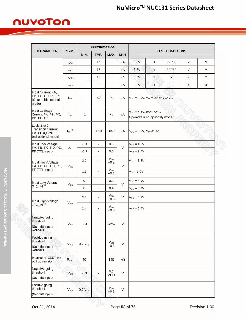
NuMicro NUC131 Series Datasheet
Oct 31, 2014 Page 58 of 75 Revision 1.00
NU
MIC
RO
™ N
UC
13
1 S
ER
IES
DA
TA
SH
EE
T
PARAMETER SYM. SPECIFICATION
TEST CONDITIONS MIN. TYP. MAX. UNIT
IPWD3 17 A 3.3V X 32.768 V V
IPWD4 17 A 3.3V X 32.768 V V
IPWD5 10 A 5.5V X X X X
IPWD6 9 A 3.3V X X X X
Input Current PA, PB, PC, PD, PE, PF (Quasi-bidirectional mode)
IIN1 -67 -75 A VDD = 5.5V, VIN = 0V or VIN=VDD
Input Leakage Current PA, PB, PC, PD, PE, PF
ILK -1 - +1 A VDD = 5.5V, 0<VIN<VDD
Open-drain or input only mode.
Logic 1 to 0 Transition Current PA~PF (Quasi-bidirectional mode)
ITL [3]
-610 -650 A VDD = 5.5V, VIN=2.0V
Input Low Voltage PA, PB, PC, PD, PE, PF (TTL input)
VIL1 -0.3 - 0.8
V VDD = 4.5V
-0.3 - 0.6 VDD = 2.5V
Input High Voltage PA, PB, PC, PD, PE, PF (TTL input)
VIH1
2.0 - VDD +0.2
V
VDD = 5.5V
1.5 - VDD +0.2
VDD =3.0V
Input Low Voltage XT1_IN
[*2]
VIL3 0 - 0.8
V VDD = 4.5V
0 - 0.4 VDD = 3.0V
Input High Voltage XT1_IN
[*2]
VIH3
3.5 - VDD +0.3
V VDD = 5.5V
2.4 - VDD +0.3
VDD = 3.0V
Negative going threshold
(Schmitt input), nRESET
VILS -0.3 - 0.2VDD V
Positive going threshold
(Schmitt input), nRESET
VIHS 0.7 VDD - VDD
+0.3 V
Internal nRESET pin pull up resistor
RRST 40 150 kΩ
Negative going threshold
(Schmitt input),
VILS -0.3 - 0.3
VDD V
Positive going threshold
(Schmitt input),
VIHS 0.7 VDD - VDD
+0.3 V

NuMicro NUC131 Series Datasheet
Oct 31, 2014 Page 59 of 75 Revision 1.00
NU
MIC
RO
™ N
UC
13
1 S
ER
IES
DA
TA
SH
EE
T
PARAMETER SYM. SPECIFICATION
TEST CONDITIONS MIN. TYP. MAX. UNIT
Source Current PA, PB, PC, PD, PE, PF (Quasi-bidirectional Mode)
ISR11 -300 -400 A VDD = 4.5V, VS = 2.4V
ISR12 -50 -80 A VDD = 2.7V, VS = 2.2V
ISR12 -40 -73 A VDD = 2.5V, VS = 2.0V
Source Current PA, PB, PC, PD, PE, PF (Push-pull Mode)
ISR21 -20 -26 mA VDD = 4.5V, VS = 2.4V
ISR22 -3 -5.2 mA VDD = 2.7V, VS = 2.2V
ISR22 -2.5 -5 mA VDD = 2.5V, VS = 2.0V
Sink Current PA, PB, PC, PD, PE, PF (Quasi-bidirectional and Push-pull Mode)
ISK1 10 17 mA VDD = 4.5V, VS = 0.45V
ISK1 6 11 mA VDD = 2.7V, VS = 0.45V
ISK1 5 10 mA VDD = 2.5V, VS = 0.45V
Note:
1. nRESET pin is a Schmitt trigger input.
2. Crystal Input is a CMOS input.
3. Pins of PA, PB, PC, PD, PE and PF can source a transition current when they are being externally driven from 1 to 0. In the condition of VDD = 5.5 V, the transition current reaches its maximum value when VIN approximates to 2 V.

NuMicro NUC131 Series Datasheet
Oct 31, 2014 Page 60 of 75 Revision 1.00
NU
MIC
RO
™ N
UC
13
1 S
ER
IES
DA
TA
SH
EE
T
8.3 AC Electrical Characteristics
8.3.1 External 4~24 MHz High Speed Oscillator
tCHCX
90%
10%
tCLCH
tCHCL
tCLCX
tCLCL
0.3 VDD
0.7 VDD
Note: Duty cycle is 50%.
SYMBOL PARAMETER CONDITION MIN. TYP. MAX. UNIT
tCHCX Clock High Time 10 - - nS
tCLCX Clock Low Time 10 - - nS
tCLCH Clock Rise Time 2 - 15 nS
tCHCL Clock Fall Time 2 - 15 nS
8.3.2 External 4~24 MHz High Speed Crystal
SYMBOL PARAMETER CONDITION MIN. TYP.. MAX. UNIT
VHXT Operation Voltage VDD - 2.5 - 5.5 V
TA Temperature - -40 - 105
IHXT Operating Current 12 MHz at VDD = 5V - 2 - mA
12 MHz at VDD = 3V 0.8 mA
fHXT Clock Frequency External crystal 4 24 MHz
8.3.2.1 Typical Crystal Application Circuits
CRYSTAL C1 C2 R
4 MHz ~ 24 MHz 10~20pF 10~20pF without

NuMicro NUC131 Series Datasheet
Oct 31, 2014 Page 61 of 75 Revision 1.00
NU
MIC
RO
™ N
UC
13
1 S
ER
IES
DA
TA
SH
EE
T
XT1_INXT1_OUT
C1RC2
Figure 8-1 Typical Crystal Application Circuit
8.3.3 Internal 22.1184 MHz High Speed Oscillator
SYMBOL PARAMETER CONDITION MIN. TYP. MAX. UNIT
VHRC Operation Voltage VDD - 2.5 - 5.5 V
fHRC
Center Frequency - - 22.1184 - MHz
Calibrated Internal Oscillator Frequency
+25; VDD =5 V -1 - +1 %
-40~+105;
VDD=2.5 V~5.5 V -2 - +2 %
IHRC Operation Current VDD =5 V - 744 - uA

NuMicro NUC131 Series Datasheet
Oct 31, 2014 Page 62 of 75 Revision 1.00
NU
MIC
RO
™ N
UC
13
1 S
ER
IES
DA
TA
SH
EE
T
Figure 8-2 HIRC Accuracy vs. Temperature
8.3.4 Internal 10 kHz Low Speed Oscillator
SYMBOL PARAMETER CONDITION MIN. TYP. MAX. UNIT
VLRC Operation Voltage VDD - 2.5 - 5.5 V
fLRC Center Frequency - - 10 - kHz
- Calibrated Internal Oscillator Frequency
+25; VDD =5 V -10 - +10 %
-40~+105;
VDD=2.5 V~5.5 V -50 - +50 %
-1.80
-1.60
-1.40
-1.20
-1.00
-0.80
-0.60
-0.40
-0.20
0.00
0.20
0.40
-40 -30 -20 -10 0 10 20 25 30 40 50 60 70 80 85 90 100110
Pe
rce
nta
ge(%
)
Temperature()
HIRC oscillator accuracy vs. temperature
Min
Max

NuMicro NUC131 Series Datasheet
Oct 31, 2014 Page 63 of 75 Revision 1.00
NU
MIC
RO
™ N
UC
13
1 S
ER
IES
DA
TA
SH
EE
T
8.4 Analog Characteristics
8.4.1 12-bit SARADC Specification
SYMBOL PARAMETER MIN. TYP. MAX. UNIT
- Resolution - - 12 Bit
DNL Differential nonlinearity error - -1~2 -1~4 LSB
INL Integral nonlinearity error - ±2 ±4 LSB
EO Offset error - 3 - LSB
EG Gain error (Transfer gain) - -3 - -
EA Absolute Error - 4 - LSB
- Monotonic Guaranteed
FADC ADC clock frequency (AVDD = 4.5V~5.5V) - - 21 MHz
FS Sample rate (FADC/TCONV) - - 1000 kSPS
TACQ Acquisition Time (Sample Stage) 2~9 1/FADC
TCONV Total Conversion Time 16~23 1/FADC
VDDA Supplt Current 3 - 5.5 V
IDDA Supply current (Avg.) 2.9 mA
VIN Input voltage 0 - AVDD V
CIN Input Capacitance 6 pF
RIN Input Load 6.5 kΩ

NuMicro NUC131 Series Datasheet
Oct 31, 2014 Page 64 of 75 Revision 1.00
NU
MIC
RO
™ N
UC
13
1 S
ER
IES
DA
TA
SH
EE
T
1
2
3
4
5
6
4095
4094
7
4093
4092
Ideal transfer curve
Actual transfer curve
Offset Error
EO
Analog input voltage
(LSB)
4095
ADC
output
code
Offset Error
EO
Gain Error
EG
EF (Full scale error) = EO + EG
DNL
1 LSB
8.4.2 LDO and Power Management Specification
SYMBOL PARAMETER MIN. TYP. MAX. UNIT NOTE
VDD Input Voltage VDD 2.5 5.5 V VDD input voltage
VLDO Output Voltage 1.62 1.8 1.98 V VDD > 2.5 V
TA Operating Temperature -40 25 105
Note:
1. It is recommended a 0.1μF bypass capacitor is connected between VDD and the closest VSS pin of the device.
2. For ensuring power stability, a 1μF Capacitor must be connected between LDO_CAP pin and the closest VSS pin of the device..

NuMicro NUC131 Series Datasheet
Oct 31, 2014 Page 65 of 75 Revision 1.00
NU
MIC
RO
™ N
UC
13
1 S
ER
IES
DA
TA
SH
EE
T
8.4.3 Low Voltage Reset Specification
SYMBOL PARAMETER CONDITION MIN. TYP. MAX. UNIT
AVDD Operation Voltage - 0 - 5.5 V
TA Quiescent Current AVDD=5.5 V - 1 5 A
ILVR Operation Temperature - -40 25 105
VLVR Threshold Voltage
TA = 25 2.00 2.0 2.4 V
TA = -40 1.95 1.98 2.02 V
TA = 105 2.04 2.13 2.25 V
8.4.4 Brown-out Detector Specification
SYMBOL PARAMETER CONDITION MIN. TYP. MAX. UNIT
AVDD Operation Voltage - 0 - 5.5 V
TA Temperature - -40 25 105
IBOD Quiescent Current AVDD=5.5 V - - 140 μA
VBOD
Brown-out Voltage (Falling edge)
BOD_VL[1:0]=11 4.45 4.53 4.56 V
BOD_VL [1:0]=10 3.74 3.8 3.84 V
BOD_VL [1:0]=01 2.73 2.77 2.8 V
BOD_VL [1:0]=00 2.22 2.25 2.28 V
VBOD Brown-out Voltage (Rising edge)
BOD_VL[1:0]=11 4.34 4.39 4.41 V
BOD_VL [1:0]=10 3.65 3.69 3.71 V
BOD_VL [1:0]=01 2.66 2.69 2.7 V
BOD_VL [1:0]=00 2.16 2.19 2.2 V
8.4.5 Power-on Reset Specification
SYMBOL PARAMETER CONDITION MIN. TYP. MAX. UNIT
TA Operation Temperature - -40 25 105
VPOR Reset Voltage V+ 1.6 2 2.4 V
VPOR VDD Start Voltage to Ensure Power-on Reset
- - - 100 mV
RRVDD VDD Raising Rate to Ensure Power-on Reset
- 0.025 - - V/ms
tPOR Minimum Time for VDD Stays at VPOR to Ensure Power-on Reset
- 0.5 - - ms

NuMicro NUC131 Series Datasheet
Oct 31, 2014 Page 66 of 75 Revision 1.00
NU
MIC
RO
™ N
UC
13
1 S
ER
IES
DA
TA
SH
EE
T
tPOR
RRVDD
VPOR
VDD
Time
Figure 8-3 Power-up Ramp Condition

NuMicro NUC131 Series Datasheet
Oct 31, 2014 Page 67 of 75 Revision 1.00
NU
MIC
RO
™ N
UC
13
1 S
ER
IES
DA
TA
SH
EE
T
8.5 Flash DC Electrical Characteristics
SYMBOL PARAMETER CONDITIONS MIN. TYP. MAX. UNIT
VFLA[1]
Supply Voltage 1.62 1.8 1.98 V[2]
NENDUR Endurance 20000 - - cycles[2]
TRET Data Retention At 85 100 - - year
TERASE Page Erase Time 20 - - ms
TMER Mass Erase Time 40 - - ms
TPROG Program Time 40 - - μs
Note:
1. VFLA is source from chip LDO output voltage 2. Number of program/erase cycles.

NuMicro NUC131 Series Datasheet
Oct 31, 2014 Page 68 of 75 Revision 1.00
NU
MIC
RO
™ N
UC
13
1 S
ER
IES
DA
TA
SH
EE
T
8.6 I2C Dynamic Characteristics
SYMBOL PARAMETER STANDARD MODE
[1][2] FAST MODE
[1][2]
UNIT MIN. MAX. MIN. MAX.
tLOW SCL low period uS
tHIGH SCL high period uS
tSU; STA Repeated START condition setup time uS
tHD; STA START condition hold time 4 - 0.6 - uS
tSU; STO STOP condition setup time 4 - 0.6 - uS
tBUF Bus free time 4.7[3]
- 1.2[3]
- uS
tSU;DAT Data setup time 250 - 100 - nS
tHD;DAT Data hold time 0[4]
3.45[5]
0[4]
0.8[5]
uS
tr SCL/SDA rise time - 1000 20+0.1Cb 300 nS
tf SCL/SDA fall time - 300 - 300 nS
Cb Capacitive load for each bus line - 400 - 400 pF
Note:
1. Guaranteed by design, not tested in production.
2. HCLK must be higher than 2 MHz to achieve the maximum standard mode I2C frequency. It must be higher than 8 MHz to achieve the maximum fast mode I2C frequency.
3. I2C controller must be retriggered immediately at slave mode after receiving STOP condition.
4. The device must internally provide a hold time of at least 300 ns for the SDA signal in order to bridge the undefined region of the falling edge of SCL.
5. The maximum hold time of the Start condition has only to be met if the interface does not stretch the low period of SCL signal.
tBUF
STOP
SDA
SCL
START
tHD;STA
tLOW
tHD;DAT
tHIGH
tf
tSU;DAT
Repeated
START
tSU;STA tSU;STO
STOP
tr
Figure 8-4 I2C Timing Diagram

NuMicro NUC131 Series Datasheet
Oct 31, 2014 Page 69 of 75 Revision 1.00
NU
MIC
RO
™ N
UC
13
1 S
ER
IES
DA
TA
SH
EE
T
8.7 SPI Dynamic Characteristics
Symbol Parameter Min. Typ. Max. Unit
SPI Master Mode (VDD = 4.5 V ~ 5.5 V, 0 pF loading Capacitor)
tDS Data setup time 0 - - ns
tDH Data hold time 4 - - ns
tV Data output valid time - 1 2 ns
SPI Master Mode (VDD = 3.0 V ~ 3.6 V, 0 pF loading Capacitor)
tDS Data setup time 0 - - ns
tDH Data hold time 4.5 - - ns
tV Data output valid time - 2 4 ns
SPI Slave Mode (VDD = 4.5 V ~ 5.5 V, 0 pF loading Capacitor)
tDS Data setup time 0 - - ns
tDH Data hold time 3.5 - - ns
tV Data output valid time - 16 22 ns
SPI Slave Mode (VDD = 3.0 V ~ 3.6 V, 0 pF loading Capacitor)
tDS Data setup time 0 - - ns
tDH Data hold time 4.5 - - ns
tV Data output valid time - 18 24 ns
Figure 8-5 SPI Master Mode Timing Diagram
CLKP=0, TX_NEG=1, RX_NEG=0
or
CLKP=1, TX_NEG=0, RX_NEG=1
CLKP=0, TX_NEG=0, RX_NEG=1
or
CLKP=1, TX_NEG=1, RX_NEG=0
MISO
MOSI Data Valid
Data ValidData Valid
Data Valid
SPICLK
MISO
MOSI Data Valid
Data ValidData Valid
Data Valid
CLKP=0
CLKP=1
tV
tDS tDH
tV
tDS tDH

NuMicro NUC131 Series Datasheet
Oct 31, 2014 Page 70 of 75 Revision 1.00
NU
MIC
RO
™ N
UC
13
1 S
ER
IES
DA
TA
SH
EE
T
Figure 8-6 SPI Slave Mode Timing Diagram
CLKP=0, TX_NEG=1, RX_NEG=0
or
CLKP=1, TX_NEG=0, RX_NEG=1
CLKP=0, TX_NEG=0, RX_NEG=1
or
CLKP=1, TX_NEG=1, RX_NEG=0MISO
MOSI Data Valid
Data ValidData Valid
Data Valid
SPICLK
MISO
MOSI Data Valid
Data ValidData Valid
Data Valid
CLKP=0
CLKP=1
tv
tDS tDH
tv
tDS tDH

NuMicro NUC131 Series Datasheet
Oct 31, 2014 Page 71 of 75 Revision 1.00
NU
MIC
RO
™ N
UC
13
1 S
ER
IES
DA
TA
SH
EE
T
8.8 I2S Dynamic Characteristics
Symbol Parameter Min Max Unit Test Conditions
tw(CKH) I2S clock high time 42 -
ns
Master fPCLK = MHz, data: 24 bits, audio frequency = 256 kHz
tw(CKL) I2S clock low time 37 -
tv(WS) WS valid time 7 - Master mode
th(WS) WS hold time 1 - Master mode
tsu(WS) WS setup time 34 - Slave mode
th(WS) WS hold time 0 - Slave mode
DuCy(SCK) I2S slave input clock
duty cycle 25 75 % Slave mode
tsu(SD_MR)
Data input setup time 0 -
ns
Master receiver
tsu(SD_SR) 0 - Slave receiver
th(SD_MR)
Data input hold time 0 - Master receiver
th(SD_SR) 0 - Slave receiver
tv(SD_ST) Data output valid time - 32 Slave transmitter (after enable edge)
th(SD_ST) Data output hold time 16 - Slave transmitter (after enable edge)
tv(SD_MT) Data output valid time - 5 Master transmitter (after enable edge)
th(SD_MT) Data output hold time 0 - Master transmitter (after enable edge)
tw(CKH)
tw(CKL) th(WS)tv(WS)
th(SD_ST)
LSB transmit(2)
MSB transmit Bitn transmit LSB transmit
LSB receive(2)
MSB receive Bitn receive LSB receive
tsu(SD_MR) th(SD_MR)
SDtransmit
SDreceive
WS output
CPOL = 1
CPOL = 0
tv(SD_ST)
CK
ou
tpu
t
Figure 8-7 I2S Master Mode Timing Diagram

NuMicro NUC131 Series Datasheet
Oct 31, 2014 Page 72 of 75 Revision 1.00
NU
MIC
RO
™ N
UC
13
1 S
ER
IES
DA
TA
SH
EE
T
tw(CKH) tw(CKL) th(WS)
tsu(WS) th(SD_ST)
LSB transmit(2)
MSB transmit Bitn transmit LSB transmit
LSB receive(2)
MSB receive Bitn receive LSB receive
tsu(SD_SR) th(SD_SR)
SDtransmit
SDreceive
WS input
CPOL = 1
CPOL = 0
tv(SD_ST)
CK
In
pu
t
Figure 8-8 I2S Slave Mode Timing Diagram

NuMicro NUC131 Series Datasheet
Oct 31, 2014 Page 73 of 75 Revision 1.00
NU
MIC
RO
™ N
UC
13
1 S
ER
IES
DA
TA
SH
EE
T
9 PACKAGE DIMENSIONS
9.1 64-pin LQFP (7x7x1.4 mm footprint 2.0 mm)

NuMicro NUC131 Series Datasheet
Oct 31, 2014 Page 74 of 75 Revision 1.00
NU
MIC
RO
™ N
UC
13
1 S
ER
IES
DA
TA
SH
EE
T
9.2 48-pin LQFP (7x7x1.4 mm footprint 2.0 mm)

NuMicro NUC131 Series Datasheet
Oct 31, 2014 Page 75 of 75 Revision 1.00
NU
MIC
RO
™ N
UC
13
1 S
ER
IES
DA
TA
SH
EE
T
10 REVISION HISTORY
REVISION DATE DESCRIPTION
1.00 Oct. 31, 2014 Preliminary version
Important Notice
Nuvoton Products are neither intended nor warranted for usage in systems or equipment, any malfunction or failure of which may cause loss of human life, bodily injury or severe property damage. Such applications are deemed, “Insecure Usage”.
Insecure usage includes, but is not limited to: equipment for surgical implementation, atomic energy control instruments, airplane or spaceship instruments, the control or operation of dynamic, brake or safety systems designed for vehicular use, traffic signal instruments, all types of safety devices, and other applications intended to support or sustain life.
All Insecure Usage shall be made at customer’s risk, and in the event that third parties lay claims to Nuvoton as a result of customer’s Insecure Usage, customer shall indemnify the damages and liabilities thus incurred by Nuvoton.