Embed Size (px)
Citation preview
NVIDIA GT640
PCIe® ADD-IN BOARD
Datasheet
GFX-N3A6-01FMS3
REV 0.1 Page 2 of 14 NOVEMBER 16, 2012
CONTENTS
1. Feature .................................................................................................................. 3
2. Functional Overview ............................................................................................. 4
2.1. GPU Block diagram .................................................................................... 4
2.2. Memory Interface ..................................................................................... 4
2.3. Features and Technologies ....................................................................... 5
2.4. Display System .......................................................................................... 5
2.5. Digital Audio .............................................................................................. 5
2.6. Video ......................................................................................................... 5
2.7. Power Management Technologies ........................................................... 6
2.8. Bus Support Features ................................................................................ 6
3. PIN Assignment and Description………………………………………………………………………..7
3.1. DVI-I Connector Pinout ............................................................................ .7
3.2. HDMI 1.3a Connector Pinout ................................................................... .7
3.3. VGA Connector Pinout ............................................................................. .8
3.4. VGA Header Pinout .................................................................................. .8
3.5. Optional DisplayPort Connector Pinoyt ................................................... .9
4. Power Specifications ........................................................................................... 10
5. Thermal Specifications ........................................................................................ 10
6. Output configuration and Board Dimension ....................................................... 11
6.1. Output Configuration .............................................................................. 11
6.2 Board Dimension .................................................................................... 12
7. Thermal Mechanism.......................................................................................... 133
REV 0.1 Page 3 of 14 NOVEMBER 16, 2012
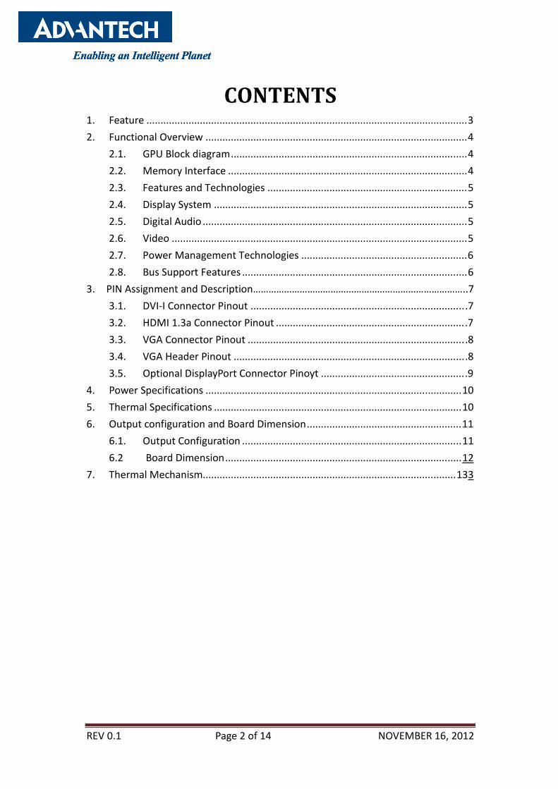
1. Feature
Model Name GFX-N3A6-01FMS3
Graphics Processing Unit
GPU GT640(GK107-300)
Process Technology 28 nm
Graphics Engine Operating
Frequency (max) 900 MHz
Form Factor Low profile (144 X 68.9 mm)
Card Interface PCI Express® 3.0 (X16)
CUDA Cores 384
Texture Fill Rate(billion/sec) 28.8
DirectX® capability DirectX® 11
Shader Model Shader Model 5.0
OpenGL OpenGL™ 4.2
Video Decoder H.264, VC-1, MPEG-2, MPEG-4 part 2 decode,
MVC, 3D Blu Ray
Memory
Memory Operating Frequency
(max) 900 MHz / 1.8 Gbps
Configuration, type 128-bit wide, 1 GB, DDR3
Display Interface
Dual-Link DVI Dual Link DVI-D
HDMI 1.4b HDMI x1
VGA VGA x1
REV 0.1 Page 4 of 14 NOVEMBER 16, 2012
2. Functional Overview
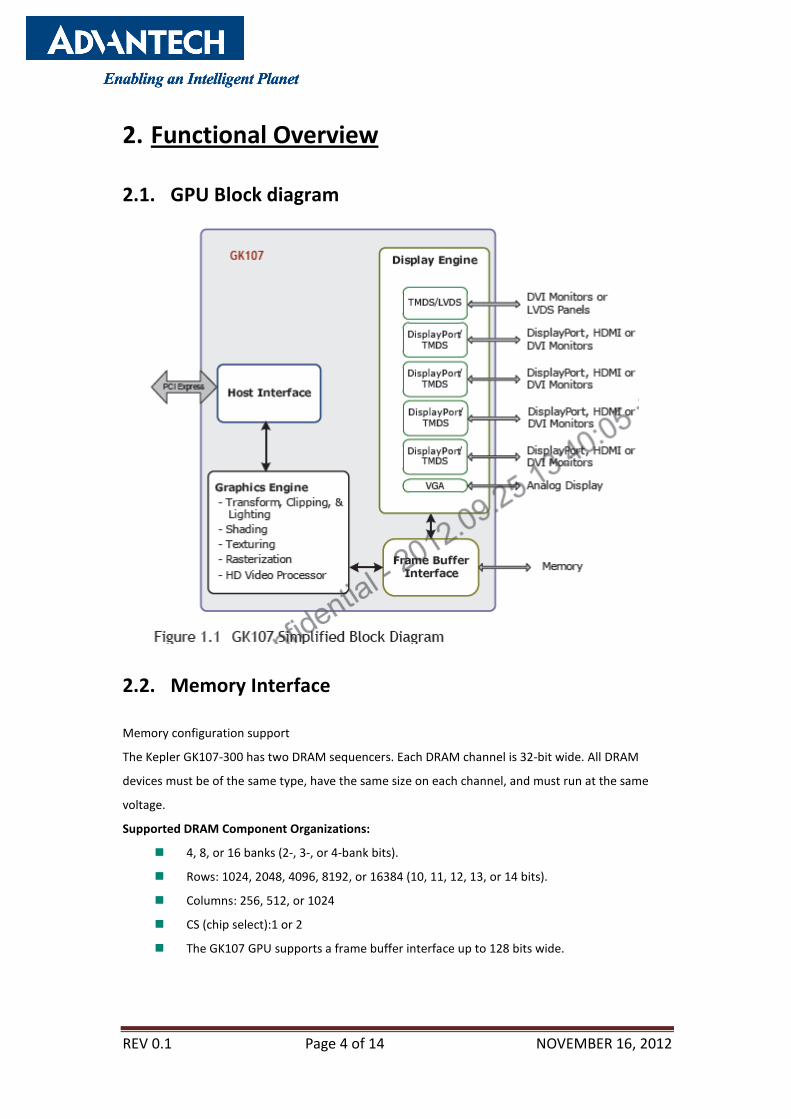
2.1. GPU Block diagram
2.2. Memory Interface
Memory configuration support
The Kepler GK107-300 has two DRAM sequencers. Each DRAM channel is 32-bit wide. All DRAM
devices must be of the same type, have the same size on each channel, and must run at the same
voltage.
Supported DRAM Component Organizations:
� 4, 8, or 16 banks (2-, 3-, or 4-bank bits).
� Rows: 1024, 2048, 4096, 8192, or 16384 (10, 11, 12, 13, or 14 bits).
� Columns: 256, 512, or 1024
� CS (chip select):1 or 2
� The GK107 GPU supports a frame buffer interface up to 128 bits wide.
REV 0.1 Page 5 of 14 NOVEMBER 16, 2012
2.3. Features and Technologies
Fully DirectX® 11 compliant and Shader Model 5.0
OpenGL 4.2
NVIDIA® Ageia PhysXTM
technology
NVIDIA® CUDA technology
2.4. Display System
Four display pipelines for quad independent display
Pipeline pixel depth 12 bits per each color
HDMI version: 1.4b (340MHz)
� Full backwards compatibility with HDMI 1.x
DisplayPort (DP) version: 1.2 (Options)
DVI-D: Dual-link resolution 2560x1600@60 Hz refresh rate
VGA support (optional standard VGA via header and cable): Maximum resolution of
2048x1536 @ 85 Hz refresh rate
2.5. Digital Audio
Supports for HD Audio over PCI Express
Support for secure premium audio (e.g. 7.1 Audio)
Data rates of 44.1KHz, 48KHz, 88.2KHz, 96KHz, 176KHz and 192KHz
Word sizes of 16-bit, 20bit, and 24-bit
2.6. Video
The following video formats are supported:
MPEG-2
MPEG-4 Part 2 Advanced Simple Profile
H.264 SVC codec support
Support for 3D Blu Ray
VC1
DivX version 3.11 and later
MVC
A fill range of video resolutions are supported including 1080p, 1080i, 720p, 480p and 480i
REV 0.1 Page 6 of 14 NOVEMBER 16, 2012
2.7. Power Management Technologies
The GK107 GPU employs enhanced power management to achieve very low GPU power
consumption. The following features are supported:
ASLM and ASPM power management
PLLs on lower voltage rails
Dynamic memory termination
Adaptive clocking
Adaptive Power States
2.8. Bus Support Features
Compliant with the PCI Express® Base Specification Revision 3.0, up to 8.0 GT/s
Supports ×1, ×2, ×4, ×8, and ×16 lane widths.
Supports 2.5 GT/s, 5.0 GT/s, and 8.0 GT/s link-data rates.
Supports ×16 lane reversal where the receivers on lanes 0 to 15 on the graphics endpoint
are mapped to the transmitters on lanes 15 down to 0 on the root complex.
Supports ×16 lane reversal where the transmitters on lanes 0 to 15 on the graphics
endpoint are mapped to the receivers on lanes 15 down to 0 on the root complex (requires
corresponding support on the root complex).
Supports full-swing and low-swing transmitter output levels.
REV 0.1 Page 7 of 14 NOVEMBER 16, 2012
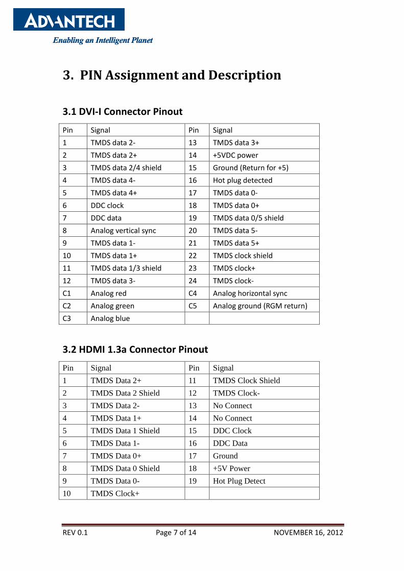
3. PIN Assignment and Description
3.1 DVI-I Connector Pinout
Pin Signal Pin Signal
1 TMDS data 2- 13 TMDS data 3+
2 TMDS data 2+ 14 +5VDC power
3 TMDS data 2/4 shield 15 Ground (Return for +5)
4 TMDS data 4- 16 Hot plug detected
5 TMDS data 4+ 17 TMDS data 0-
6 DDC clock 18 TMDS data 0+
7 DDC data 19 TMDS data 0/5 shield
8 Analog vertical sync 20 TMDS data 5-
9 TMDS data 1- 21 TMDS data 5+
10 TMDS data 1+ 22 TMDS clock shield
11 TMDS data 1/3 shield 23 TMDS clock+
12 TMDS data 3- 24 TMDS clock-
C1 Analog red C4 Analog horizontal sync
C2 Analog green C5 Analog ground (RGM return)
C3 Analog blue
3.2 HDMI 1.3a Connector Pinout
Pin Signal Pin Signal
1 TMDS Data 2+ 11 TMDS Clock Shield
2 TMDS Data 2 Shield 12 TMDS Clock-
3 TMDS Data 2- 13 No Connect
4 TMDS Data 1+ 14 No Connect
5 TMDS Data 1 Shield 15 DDC Clock
6 TMDS Data 1- 16 DDC Data
7 TMDS Data 0+ 17 Ground
8 TMDS Data 0 Shield 18 +5V Power
9 TMDS Data 0- 19 Hot Plug Detect
10 TMDS Clock+
REV 0.1 Page 8 of 14 NOVEMBER 16, 2012
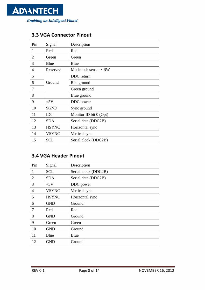
3.3 VGA Connector Pinout
Pin Signal Description
1 Red Red
2 Green Green
3 Blue Blue
4 Reserved Macintosh sense ,RW
5
Ground
DDC return
6 Red ground
7 Green ground
8 Blue ground
9 +5V DDC power
10 SGND Sync ground
11 ID0 Monitor ID bit 0 (Opt)
12 SDA Serial data (DDC2B)
13 HSYNC Horizontal sync
14 VSYNC Vertical sync
15 SCL Serial clock (DDC2B)
3.4 VGA Header Pinout
Pin Signal Description
1 SCL Serial clock (DDC2B)
2 SDA Serial data (DDC2B)
3 +5V DDC power
4 VSYNC Vertical sync
5 HSYNC Horizontal sync
6 GND Ground
7 Red Red
8 GND Ground
9 Green Green
10 GND Ground
11 Blue Blue
12 GND Ground
REV 0.1 Page 9 of 14 NOVEMBER 16, 2012
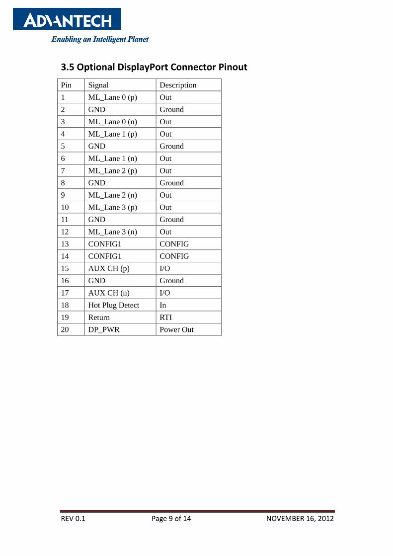
3.5 Optional DisplayPort Connector Pinout
Pin Signal Description
1 ML_Lane 0 (p) Out
2 GND Ground
3 ML_Lane 0 (n) Out
4 ML_Lane 1 (p) Out
5 GND Ground
6 ML_Lane 1 (n) Out
7 ML_Lane 2 (p) Out
8 GND Ground
9 ML_Lane 2 (n) Out
10 ML_Lane 3 (p) Out
11 GND Ground
12 ML_Lane 3 (n) Out
13 CONFIG1 CONFIG
14 CONFIG1 CONFIG
15 AUX CH (p) I/O
16 GND Ground
17 AUX CH (n) I/O
18 Hot Plug Detect In
19 Return RTI
20 DP_PWR Power Out
REV 0.1 Page 10 of 14 NOVEMBER 16, 2012
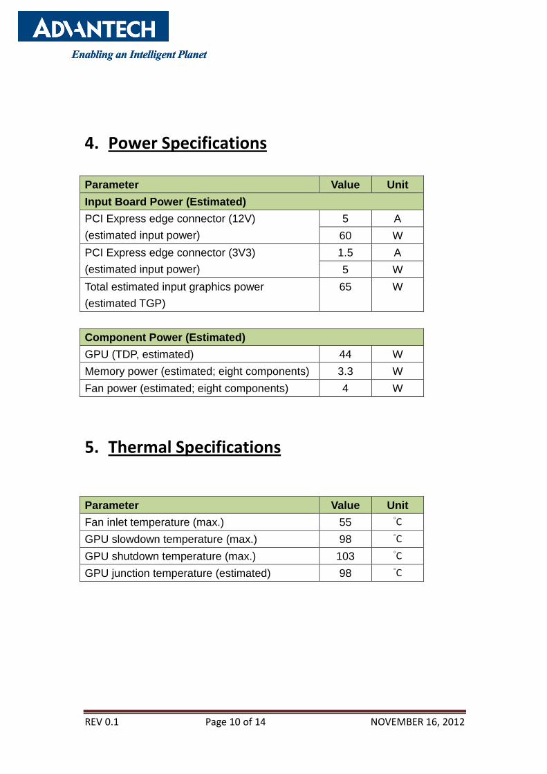
4. Power Specifications
Parameter Value Unit
Input Board Power (Estimated)
PCI Express edge connector (12V)
(estimated input power)
5 A
60 W
PCI Express edge connector (3V3)
(estimated input power)
1.5 A
5 W
Total estimated input graphics power
(estimated TGP)
65 W
Component Power (Estimated)
GPU (TDP, estimated) 44 W
Memory power (estimated; eight components) 3.3 W
Fan power (estimated; eight components) 4 W
5. Thermal Specifications
Parameter Value Unit
Fan inlet temperature (max.) 55 °C
GPU slowdown temperature (max.) 98 °C
GPU shutdown temperature (max.) 103 °C
GPU junction temperature (estimated) 98 °C
REV 0.1
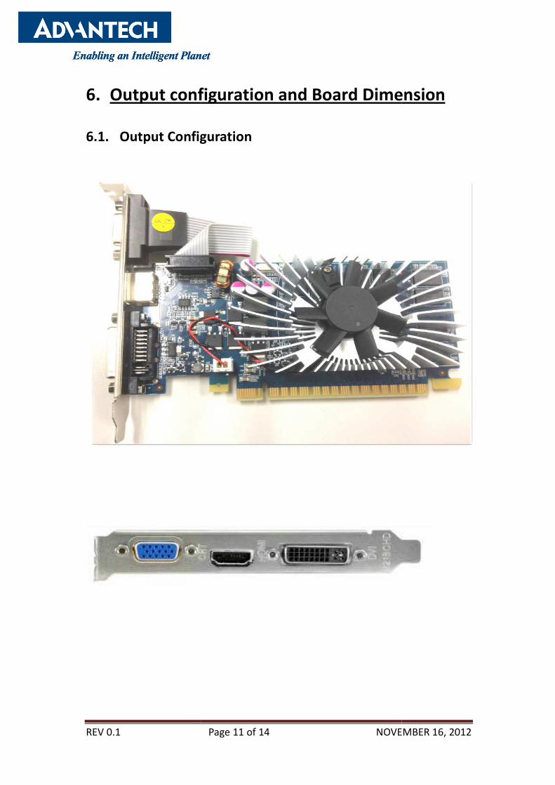
6. Output configuration and Board Dimension
6.1. Output Configuration
Page 11 of 14 NOVEMBER
Output configuration and Board Dimension
onfiguration
NOVEMBER 16, 2012
Output configuration and Board Dimension
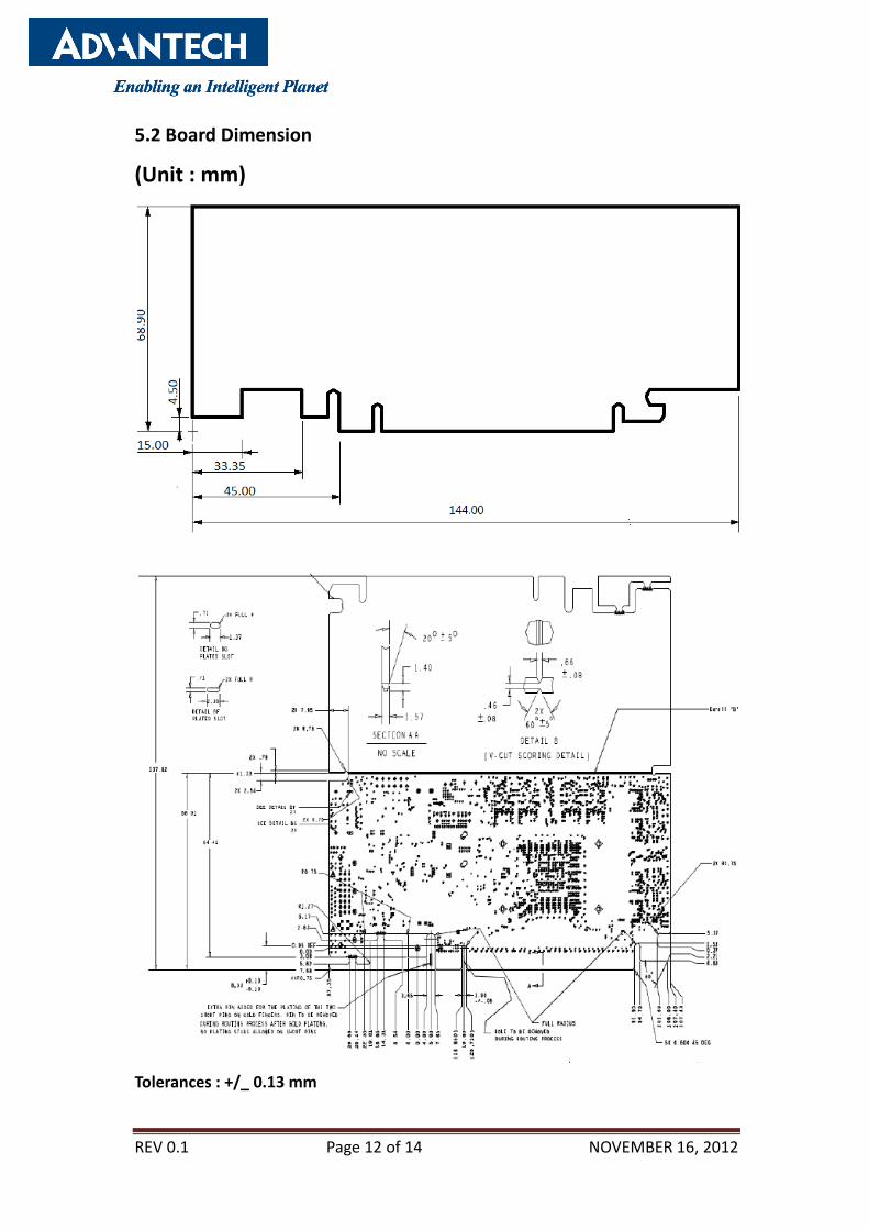
REV 0.1 Page 12 of 14 NOVEMBER 16, 2012
5.2 Board Dimension
(Unit : mm)
Tolerances : +/_ 0.13 mm
REV 0.1 Page 13 of 14 NOVEMBER 16, 2012
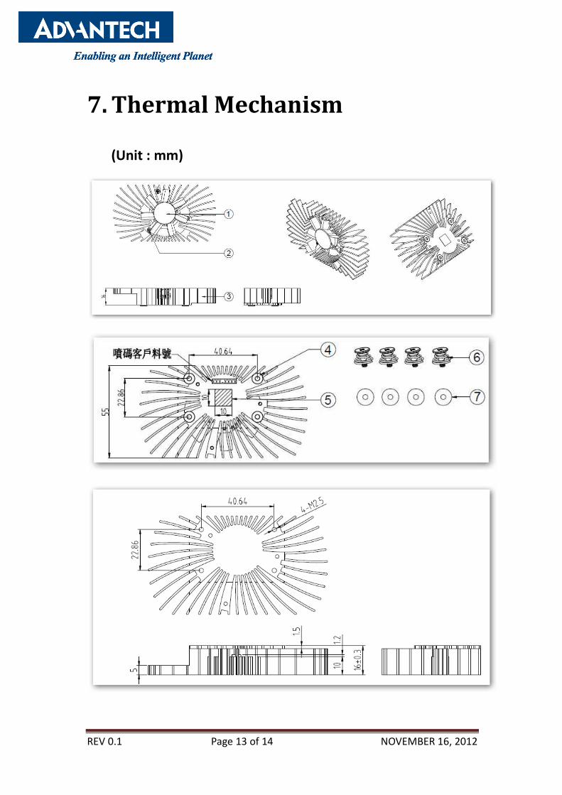
7. Thermal Mechanism
(Unit : mm)
REV 0.1 Page 14 of 14 NOVEMBER 16, 2012
Change log or update history
Rev.Rev.Rev.Rev. DataDataDataData HistoryHistoryHistoryHistory
0.1 2012/11/16 1. 1st Draft