Embed Size (px)
Citation preview
1. General description
The NX3L4053 is a triple low-ohmic single-pole double-throw analog switch, suitable for use as an analog or digital multiplexer/demultiplexer. Each switch has a digital select input (nS), two independent inputs/outputs (nY0 and nY1) and a common input/output (nZ). All three switches share an enable input (E). A digital enable pin E is common to all switches.When E is HIGH, the switches are turned off.
Schmitt trigger action at the digital inputs makes the circuit tolerant to slower input rise and fall times. Low threshold digital inputs allows this device to be driven by 1.8 V logic levels in 3.3 V applications without significant increase in supply current ICC. This makes it possible for the NX3L4053 to switch 4.3 V signals with a 1.8 V digital controller, eliminating the need for logic level translation. The NX3L4053 allows signals with amplitude up to VCC to be transmitted from nZ to nY0 or nY1; or from nY0 or nY1 to nZ. Its low ON resistance (0.5 ) and flatness (0.13 ) ensures minimal attenuation and distortion of transmitted signals.
2. Features and benefits
Wide supply voltage range from 1.4 V to 4.3 V
Very low ON resistance (peak):
1.8 (typical) at VCC = 1.4 V
1.0 (typical) at VCC = 1.65 V
0.6 (typical) at VCC = 2.3 V
0.6 (typical) at VCC = 2.7 V
0.5 (typical) at VCC = 4.3 V
Break-before-make switching
High noise immunity
ESD protection:
HBM JESD22-A114F Class 3A exceeds 4000 V
MM JESD22-A115-A exceeds 200 V
CDM AEC-Q100-011 revision B exceeds 1000 V
IEC61000-4-2 contact discharge exceeds 6000 V for switch ports
CMOS low-power consumption
Latch-up performance exceeds 100 mA per JESD 78 Class II Level A
1.8 V control logic at VCC = 3.6 V
Control input accepts voltages above supply voltage
Very low supply current, even when input is below VCC
High current handling capability (350 mA continuous current under 3.3 V supply)
Specified from 40 C to +85 C and from 40 C to +125 C
NX3L4053Triple low-ohmic single-pole double-throw analog switchRev. 5 — 25 June 2012 Product data sheet
NXP Semiconductors NX3L4053Triple low-ohmic single-pole double-throw analog switch
3. Applications
Cell phone
PDA
Portable media player
Analog multiplexing and demultiplexing
Digital multiplexing and demultiplexing
Signal gating
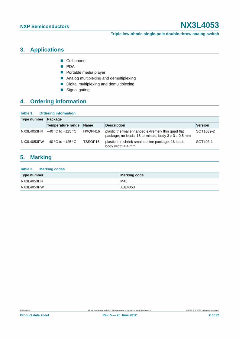
4. Ordering information
5. Marking
Table 1. Ordering information
Type number Package
Temperature range Name Description Version
NX3L4053HR 40 C to +125 C HXQFN16 plastic thermal enhanced extremely thin quad flat package; no leads; 16 terminals; body 3 3 0.5 mm
SOT1039-2
NX3L4053PW 40 C to +125 C TSSOP16 plastic thin shrink small outline package; 16 leads; body width 4.4 mm
SOT403-1
Table 2. Marking codes
Type number Marking code
NX3L4053HR M43
NX3L4053PW X3L4053
NX3L4053 All information provided in this document is subject to legal disclaimers. © NXP B.V. 2012. All rights reserved.
Product data sheet Rev. 5 — 25 June 2012 2 of 22
NXP Semiconductors NX3L4053Triple low-ohmic single-pole double-throw analog switch
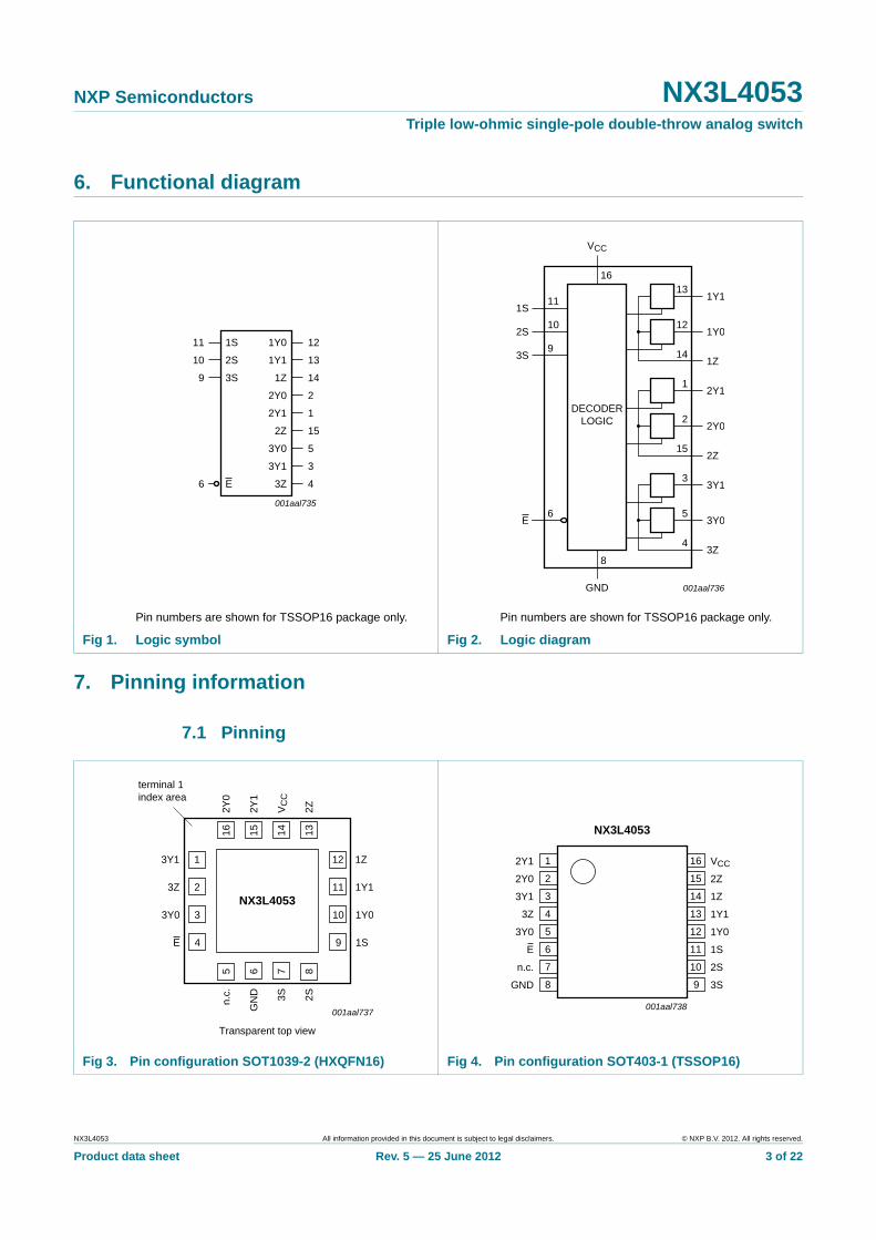
6. Functional diagram
7. Pinning information
7.1 Pinning
Pin numbers are shown for TSSOP16 package only. Pin numbers are shown for TSSOP16 package only.
Fig 1. Logic symbol Fig 2. Logic diagram
001aal735
11 1S 1Y0 12
10 2S 1Y1 13
9 3S 1Z 14
2Y0 2
2Y1 1
2Z 15
3Y0 5
3Y1 3
6 E 3Z 4
001aal736
DECODERLOGIC
1Y113
1Y012
1Z14
1S11
16
VCC
8
GND
2S10
3S9
E6
2Y11
2Y02
2Z15
3Y13
3Y05
3Z4
Fig 3. Pin configuration SOT1039-2 (HXQFN16) Fig 4. Pin configuration SOT403-1 (TSSOP16)
1
2
3
4
3Y1
3Z
3Y0NX3L4053
E
12
11
10
9
1Z
1Y1
1Y0
1S
16 15 14 13
2Y0
2Y1
VC
C
2Z
5 6 7 8
n.c.
GN
D 3S 2S
001aal737
Transparent top view
terminal 1index area
NX3L4053
2Y1 VCC
2Y0 2Z
3Y1 1Z
3Z 1Y1
3Y0 1Y0
E 1S
n.c. 2S
GND 3S
001aal738
1
2
3
4
5
6
7
8
10
9
12
11
14
13
16
15
NX3L4053 All information provided in this document is subject to legal disclaimers. © NXP B.V. 2012. All rights reserved.
Product data sheet Rev. 5 — 25 June 2012 3 of 22
NXP Semiconductors NX3L4053Triple low-ohmic single-pole double-throw analog switch
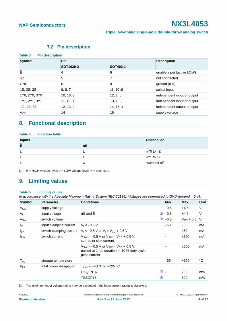
7.2 Pin description
8. Functional description
[1] H = HIGH voltage level; L = LOW voltage level; X = don’t care.
9. Limiting values
[1] The minimum input voltage rating may be exceeded if the input current rating is observed.
Table 3. Pin description
Symbol Pin Description
SOT1039-2 SOT403-1
E 4 6 enable input (active LOW)
n.c. 5 7 not connected
GND 6 8 ground (0 V)
1S, 2S, 3S 9, 8, 7 11, 10 ,9 select input
1Y0, 2Y0, 3Y0 10, 16, 3 12, 2, 5 independent input or output
1Y1, 2Y1, 3Y1 11, 15, 1 13, 1, 3 independent input or output
1Z , 2Z, 3Z 12, 13, 2 14, 15, 4 independent output or input
VCC 14 16 supply voltage
Table 4. Function table
Inputs Channel on
E nS
L L nY0 to nZ
L H nY1 to nZ
H X switches off
Table 5. Limiting valuesIn accordance with the Absolute Maximum Rating System (IEC 60134). Voltages are referenced to GND (ground = 0 V).
Symbol Parameter Conditions Min Max Unit
VCC supply voltage 0.5 +4.6 V
VI input voltage nS and E [1] 0.5 +4.6 V
VSW switch voltage [2] 0.5 VCC + 0.5 V
IIK input clamping current VI < 0.5 V 50 - mA
ISK switch clamping current VI < 0.5 V or VI > VCC + 0.5 V - 50 mA
ISW switch current VSW > 0.5 V or VSW < VCC + 0.5 V; source or sink current
- 350 mA
VSW > 0.5 V or VSW < VCC + 0.5 V; pulsed at 1 ms duration, < 10 % duty cycle; peak current
- 500 mA
Tstg storage temperature 65 +150 C
Ptot total power dissipation Tamb = 40 C to +125 C
HXQFN16 [3] - 250 mW
TSSOP16 [4] - 500 mW
NX3L4053 All information provided in this document is subject to legal disclaimers. © NXP B.V. 2012. All rights reserved.
Product data sheet Rev. 5 — 25 June 2012 4 of 22
NXP Semiconductors NX3L4053Triple low-ohmic single-pole double-throw analog switch
[2] The minimum and maximum switch voltage ratings may be exceeded if the switch clamping current rating is observed but may not exceed 4.6 V.
[3] For HXQFN16 package: above 135 C the value of Ptot derates linearly with 16.9 mW/K.
[4] For TSSOP16 package: above 60 C the value of Ptot derates linearly with 5.5 mW/K.
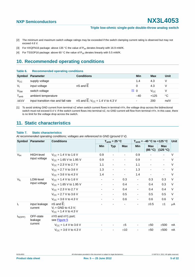
10. Recommended operating conditions
[1] To avoid sinking GND current from terminal nZ when switch current flows in terminal nYn, the voltage drop across the bidirectional switch must not exceed 0.4 V. If the switch current flows into terminal nZ, no GND current will flow from terminal nYn. In this case, there is no limit for the voltage drop across the switch.
11. Static characteristics
Table 6. Recommended operating conditions
Symbol Parameter Conditions Min Max Unit
VCC supply voltage 1.4 4.3 V
VI input voltage nS and E 0 4.3 V
VSW switch voltage [1] 0 VCC V
Tamb ambient temperature 40 +125 C
t/V input transition rise and fall rate nS and E; VCC = 1.4 V to 4.3 V - 200 ns/V
Table 7. Static characteristicsAt recommended operating conditions; voltages are referenced to GND (ground 0 V).
Symbol Parameter Conditions Tamb = 25 C Tamb = 40 C to +125 C Unit
Min Typ Max Min Max (85 C)
Max (125 C)
VIH HIGH-level input voltage
VCC = 1.4 V to 1.6 V 0.9 - - 0.9 - - V
VCC = 1.65 V to 1.95 V 0.9 - - 0.9 - - V
VCC = 2.3 V to 2.7 V 1.1 - - 1.1 - - V
VCC = 2.7 V to 3.6 V 1.3 - - 1.3 - - V
VCC = 3.6 V to 4.3 V 1.4 - - 1.4 - - V
VIL LOW-level input voltage
VCC = 1.4 V to 1.6 V - - 0.3 - 0.3 0.3 V
VCC = 1.65 V to 1.95 V - - 0.4 - 0.4 0.3 V
VCC = 2.3 V to 2.7 V - - 0.4 - 0.4 0.4 V
VCC = 2.7 V to 3.6 V - - 0.5 - 0.5 0.5 V
VCC = 3.6 V to 4.3 V - - 0.6 - 0.6 0.6 V
II input leakage current
nS and E; VI = GND to 4.3 V; VCC = 1.4 V to 4.3 V
- - - - 0.5 1 A
IS(OFF) OFF-state leakage current
nY0 and nY1 port; see Figure 5
VCC = 1.4 V to 3.6 V - - 5 - 50 500 nA
VCC = 3.6 V to 4.3 V - - 10 - 50 500 nA
NX3L4053 All information provided in this document is subject to legal disclaimers. © NXP B.V. 2012. All rights reserved.
Product data sheet Rev. 5 — 25 June 2012 5 of 22
NXP Semiconductors NX3L4053Triple low-ohmic single-pole double-throw analog switch
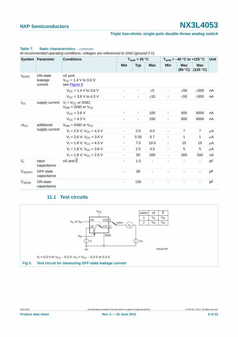
11.1 Test circuits
IS(ON) ON-state leakage current
nZ port; VCC = 1.4 V to 3.6 V; see Figure 6
VCC = 1.4 V to 3.6 V - - 5 - 50 500 nA
VCC = 3.6 V to 4.3 V - - 10 - 50 500 nA
ICC supply current VI = VCC or GND; VSW = GND or VCC
VCC = 3.6 V - - 100 - 500 5000 nA
VCC = 4.3 V - - 150 - 800 6000 nA
ICC additional supply current
VSW = GND or VCC
VI = 2.6 V; VCC = 4.3 V - 2.0 4.0 - 7 7 A
VI = 2.6 V; VCC = 3.6 V - 0.35 0.7 - 1 1 A
VI = 1.8 V; VCC = 4.3 V - 7.0 10.0 - 15 15 A
VI = 1.8 V; VCC = 3.6 V - 2.5 4.0 - 5 5 A
VI = 1.8 V; VCC = 2.5 V - 50 200 - 300 500 nA
CI input capacitance
nS and E - 1.0 - - - - pF
CS(OFF) OFF-state capacitance
- 35 - - - - pF
CS(ON) ON-state capacitance
- 130 - - - - pF
Table 7. Static characteristics …continuedAt recommended operating conditions; voltages are referenced to GND (ground 0 V).
Symbol Parameter Conditions Tamb = 25 C Tamb = 40 C to +125 C Unit
Min Typ Max Min Max (85 C)
Max (125 C)
VI = 0.3 V or VCC 0.3 V; VO = VCC 0.3 V or 0.3 V.
Fig 5. Test circuit for measuring OFF-state leakage current
IS
001aal739
VCC
VIL or VIH
VIH
VI VO
E
nY0
nY1
nS
GND
nZswitch
1
2
VIL
VIH
VIH
VIH
nSswitch
1
2
E
NX3L4053 All information provided in this document is subject to legal disclaimers. © NXP B.V. 2012. All rights reserved.
Product data sheet Rev. 5 — 25 June 2012 6 of 22
NXP Semiconductors NX3L4053Triple low-ohmic single-pole double-throw analog switch
11.2 ON resistance
[1] For NX3L4053PW (TSSOP16 package), all ON resistance values are up to 0.05 higher.
[2] Typical values are measured at Tamb = 25 C.
[3] Measured at identical VCC, temperature and input voltage.
[4] Flatness is defined as the difference between the maximum and minimum value of ON resistance measured at identical VCC and temperature.
VI = 0.3 V or VCC 0.3 V; VO = VCC 0.3 V or 0.3 V.
Fig 6. Test circuit for measuring ON-state leakage current
IS
001aal740
VCC
VIL or VIH
VIL
VI VO
E
nY0
nY1
nS
GND
nZswitch
1
2
VIL
VIH
VIL
VIL
nSswitch
1
2
E
Table 8. ON resistance[1]
At recommended operating conditions; voltages are referenced to GND (ground = 0 V); for graphs see Figure 8 to Figure 14.
Symbol Parameter Conditions Tamb = 40 C to +85 C Tamb = 40 C to +125 C Unit
Min Typ[2] Max Min Max
RON(peak) ON resistance (peak)
VI = GND to VCC; ISW = 100 mA; see Figure 7
VCC = 1.4 V - 1.8 3.8 - 4.2
VCC = 1.65 V - 1.0 1.7 - 1.8
VCC = 2.3 V - 0.6 0.9 - 1.0
VCC = 2.7 V - 0.6 0.80 - 1.0
VCC = 4.3 V - 0.5 0.80 - 1.0
RON ON resistance mismatch between channels
VI = GND to VCC; ISW = 100 mA
[3]
VCC = 1.4 V; VSW = 0.4 V - 0.23 0.38 - 0.38
VCC = 1.65 V; VSW = 0.5 V - 0.23 0.28 - 0.38
VCC = 2.3 V; VSW = 0.7 V - 0.12 0.15 - 0.18
VCC = 2.7 V; VSW = 0.8 V - 0.12 0.15 - 0.18
VCC = 4.3 V; VSW = 0.8 V - 0.12 0.15 - 0.18
RON(flat) ON resistance (flatness)
VI = GND to VCC; ISW = 100 mA
[4]
VCC = 1.4 V - 1.0 3.3 - 3.6
VCC = 1.65 V - 0.5 1.2 - 1.3
VCC = 2.3 V - 0.15 0.3 - 0.35
VCC = 2.7 V - 0.13 0.3 - 0.35
VCC = 4.3 V - 0.2 0.4 - 0.45
NX3L4053 All information provided in this document is subject to legal disclaimers. © NXP B.V. 2012. All rights reserved.
Product data sheet Rev. 5 — 25 June 2012 7 of 22
NXP Semiconductors NX3L4053Triple low-ohmic single-pole double-throw analog switch
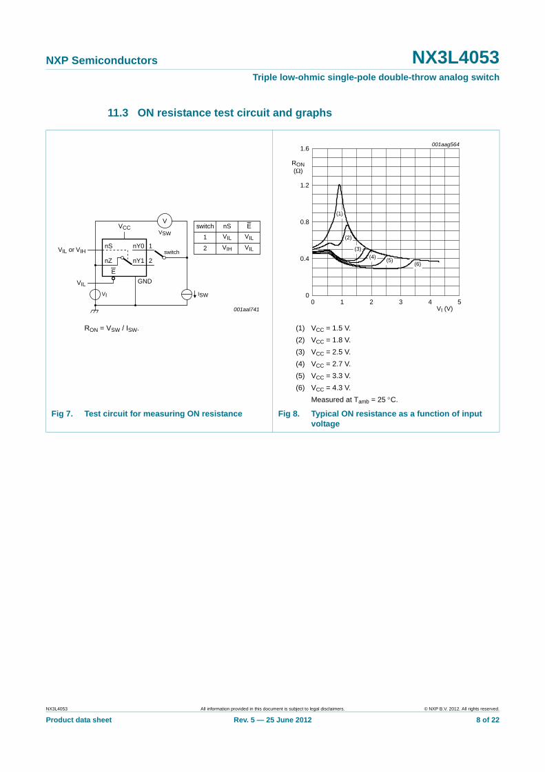
11.3 ON resistance test circuit and graphs
RON = VSW / ISW. (1) VCC = 1.5 V.
(2) VCC = 1.8 V.
(3) VCC = 2.5 V.
(4) VCC = 2.7 V.
(5) VCC = 3.3 V.
(6) VCC = 4.3 V.
Measured at Tamb = 25 C.
Fig 7. Test circuit for measuring ON resistance Fig 8. Typical ON resistance as a function of input voltage
V
001aal741
VCC
VIL or VIH
VIL
E
nY0
nY1
nS
GND
nZswitch
1
2
VIL
VIH
VIL
VIL
nSswitch
1
2
E
VI ISW
VSW
VI (V)0 5431 2
001aag564
0.8
0.4
1.2
1.6
RON(Ω)
0
(1)
(2)
(5)(6)
(4)(3)
NX3L4053 All information provided in this document is subject to legal disclaimers. © NXP B.V. 2012. All rights reserved.
Product data sheet Rev. 5 — 25 June 2012 8 of 22
NXP Semiconductors NX3L4053Triple low-ohmic single-pole double-throw analog switch
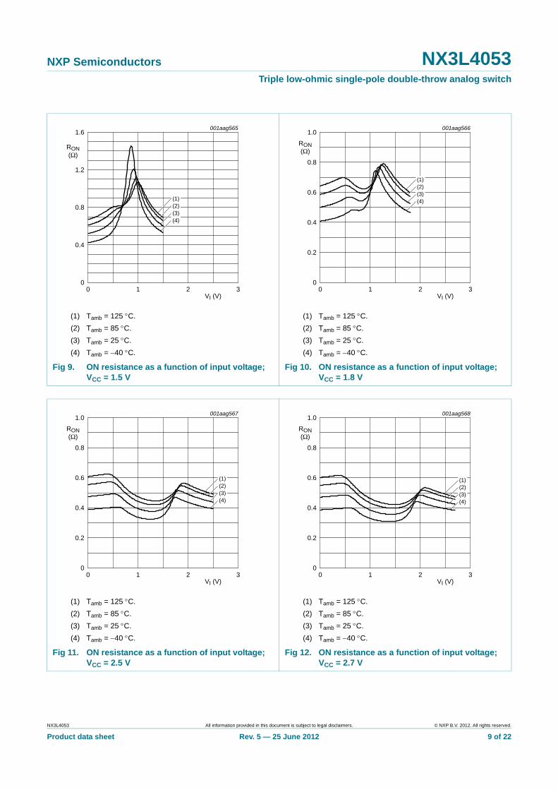
(1) Tamb = 125 C.
(2) Tamb = 85 C.
(3) Tamb = 25 C.
(4) Tamb = 40 C.
(1) Tamb = 125 C.
(2) Tamb = 85 C.
(3) Tamb = 25 C.
(4) Tamb = 40 C.
Fig 9. ON resistance as a function of input voltage; VCC = 1.5 V
Fig 10. ON resistance as a function of input voltage; VCC = 1.8 V
001aag565
VI (V)0 321
0.8
0.4
1.2
1.6
RON(Ω)
0
(1)(2)(3)(4)
001aag566
VI (V)0 321
0.4
0.6
0.2
0.8
1.0
RON(Ω)
0
(1)(2)(3)(4)
(1) Tamb = 125 C.
(2) Tamb = 85 C.
(3) Tamb = 25 C.
(4) Tamb = 40 C.
(1) Tamb = 125 C.
(2) Tamb = 85 C.
(3) Tamb = 25 C.
(4) Tamb = 40 C.
Fig 11. ON resistance as a function of input voltage; VCC = 2.5 V
Fig 12. ON resistance as a function of input voltage; VCC = 2.7 V
001aag567
VI (V)0 321
0.4
0.6
0.2
0.8
1.0
RON(Ω)
0
(1)(2)(3)(4)
001aag568
VI (V)0 321
0.4
0.6
0.2
0.8
1.0
RON(Ω)
0
(1)(2)(3)(4)
NX3L4053 All information provided in this document is subject to legal disclaimers. © NXP B.V. 2012. All rights reserved.
Product data sheet Rev. 5 — 25 June 2012 9 of 22
NXP Semiconductors NX3L4053Triple low-ohmic single-pole double-throw analog switch
12. Dynamic characteristics
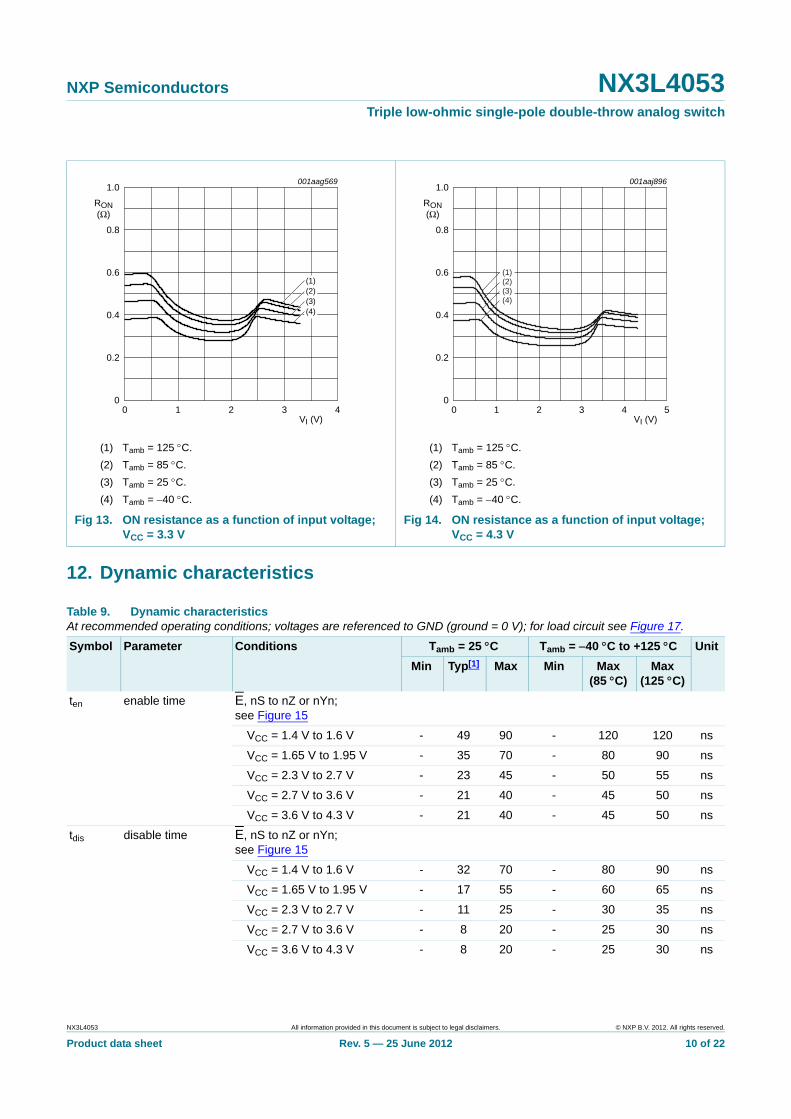
(1) Tamb = 125 C.
(2) Tamb = 85 C.
(3) Tamb = 25 C.
(4) Tamb = 40 C.
(1) Tamb = 125 C.
(2) Tamb = 85 C.
(3) Tamb = 25 C.
(4) Tamb = 40 C.
Fig 13. ON resistance as a function of input voltage; VCC = 3.3 V
Fig 14. ON resistance as a function of input voltage; VCC = 4.3 V
VI (V)0 431 2
001aag569
0.4
0.6
0.2
0.8
1.0
RON(Ω)
0
(1)(2)(3)(4)
VI (V)0 542 31
001aaj896
0.4
0.6
0.2
0.8
1.0
RON(Ω)
0
(1)(2)(3)(4)
Table 9. Dynamic characteristicsAt recommended operating conditions; voltages are referenced to GND (ground = 0 V); for load circuit see Figure 17.
Symbol Parameter Conditions Tamb = 25 C Tamb = 40 C to +125 C Unit
Min Typ[1] Max Min Max (85 C)
Max (125 C)
ten enable time E, nS to nZ or nYn; see Figure 15
VCC = 1.4 V to 1.6 V - 49 90 - 120 120 ns
VCC = 1.65 V to 1.95 V - 35 70 - 80 90 ns
VCC = 2.3 V to 2.7 V - 23 45 - 50 55 ns
VCC = 2.7 V to 3.6 V - 21 40 - 45 50 ns
VCC = 3.6 V to 4.3 V - 21 40 - 45 50 ns
tdis disable time E, nS to nZ or nYn; see Figure 15
VCC = 1.4 V to 1.6 V - 32 70 - 80 90 ns
VCC = 1.65 V to 1.95 V - 17 55 - 60 65 ns
VCC = 2.3 V to 2.7 V - 11 25 - 30 35 ns
VCC = 2.7 V to 3.6 V - 8 20 - 25 30 ns
VCC = 3.6 V to 4.3 V - 8 20 - 25 30 ns
NX3L4053 All information provided in this document is subject to legal disclaimers. © NXP B.V. 2012. All rights reserved.
Product data sheet Rev. 5 — 25 June 2012 10 of 22
NXP Semiconductors NX3L4053Triple low-ohmic single-pole double-throw analog switch
[1] Typical values are measured at Tamb = 25 C and VCC = 1.5 V, 1.8 V, 2.5 V, 3.3 V and 4.3 V respectively.
[2] Break-before-make guaranteed by design.
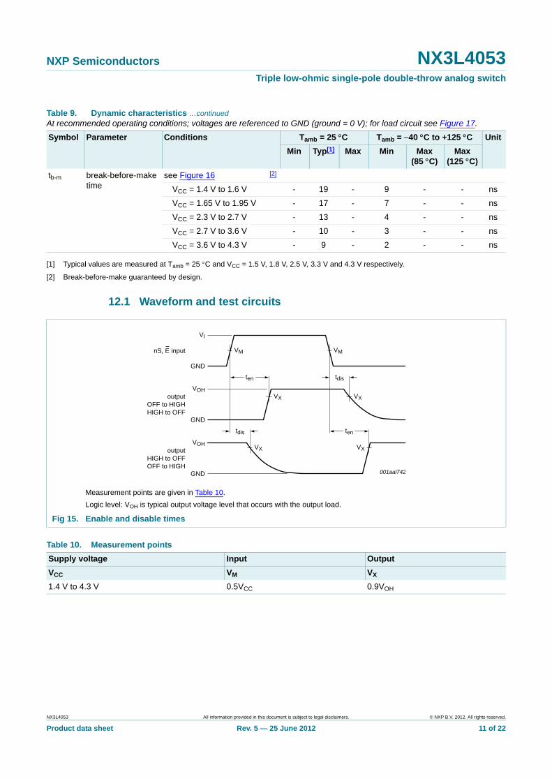
12.1 Waveform and test circuits
tb-m break-before-make time
see Figure 16 [2]
VCC = 1.4 V to 1.6 V - 19 - 9 - - ns
VCC = 1.65 V to 1.95 V - 17 - 7 - - ns
VCC = 2.3 V to 2.7 V - 13 - 4 - - ns
VCC = 2.7 V to 3.6 V - 10 - 3 - - ns
VCC = 3.6 V to 4.3 V - 9 - 2 - - ns
Table 9. Dynamic characteristics …continuedAt recommended operating conditions; voltages are referenced to GND (ground = 0 V); for load circuit see Figure 17.
Symbol Parameter Conditions Tamb = 25 C Tamb = 40 C to +125 C Unit
Min Typ[1] Max Min Max (85 C)
Max (125 C)
Measurement points are given in Table 10.
Logic level: VOH is typical output voltage level that occurs with the output load.
Fig 15. Enable and disable times
001aal742
VM
VI
VOH
VOH
GND
outputOFF to HIGHHIGH to OFF
outputHIGH to OFFOFF to HIGH
GND
GND
VM
VX VX
VX VX
tdis ten
ten tdis
nS, E input
Table 10. Measurement points
Supply voltage Input Output
VCC VM VX
1.4 V to 4.3 V 0.5VCC 0.9VOH
NX3L4053 All information provided in this document is subject to legal disclaimers. © NXP B.V. 2012. All rights reserved.
Product data sheet Rev. 5 — 25 June 2012 11 of 22
NXP Semiconductors NX3L4053Triple low-ohmic single-pole double-throw analog switch
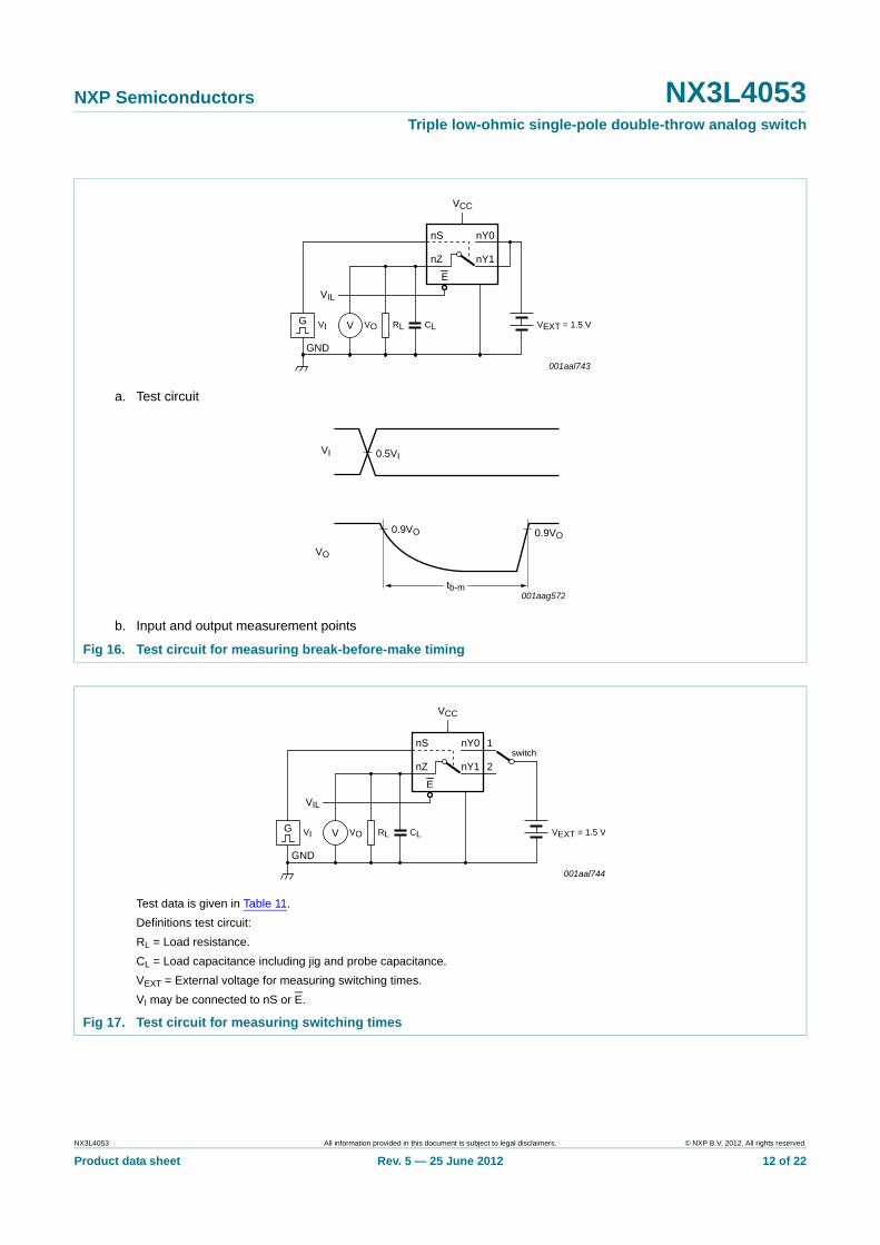
a. Test circuit
b. Input and output measurement points
Fig 16. Test circuit for measuring break-before-make timing
V
001aal743
VCC
VIL
E
nY0
nY1
nS
GND
nZ
G VEXT = 1.5 VVI VO CLRL
001aag572
VI
tb-m
VO
0.9VO0.9VO
0.5VI
Test data is given in Table 11.
Definitions test circuit:
RL = Load resistance.
CL = Load capacitance including jig and probe capacitance.
VEXT = External voltage for measuring switching times.
VI may be connected to nS or E.
Fig 17. Test circuit for measuring switching times
V
001aal744
VCC
VIL
E
nY0
nY1
nS
GND
nZ
G VEXT = 1.5 VVI VO CLRL
switch1
2
NX3L4053 All information provided in this document is subject to legal disclaimers. © NXP B.V. 2012. All rights reserved.
Product data sheet Rev. 5 — 25 June 2012 12 of 22
NXP Semiconductors NX3L4053Triple low-ohmic single-pole double-throw analog switch
12.2 Additional dynamic characteristics
[1] fi is biased at 0.5VCC.
Table 11. Test data
Supply voltage Input Load
VCC VI tr, tf CL RL
1.4 V to 4.3 V VCC 2.5 ns 35 pF 50
Table 12. Additional dynamic characteristicsAt recommended operating conditions; voltages are referenced to GND (ground = 0 V); VI = GND or VCC (unless otherwise specified); tr = tf 2.5 ns; Tamb = 25 C.
Symbol Parameter Conditions Min Typ Max Unit
THD total harmonic distortion
fi = 20 Hz to 20 kHz; RL = 32 ; see Figure 18 [1]
VCC = 1.4 V; VI = 1 V (p-p) - 0.15 - %
VCC = 1.65 V; VI = 1.2 V (p-p) - 0.10 - %
VCC = 2.3 V; VI = 1.5 V (p-p) - 0.02 - %
VCC = 2.7 V; VI = 2 V (p-p) - 0.02 - %
VCC = 4.3 V; VI = 2 V (p-p) - 0.02 - %
f(3dB) 3 dB frequency response
RL = 50 ; see Figure 19 [1]
VCC = 1.4 V to 4.3 V - 60 - MHz
iso isolation (OFF-state) fi = 100 kHz; RL = 50 ; see Figure 20 [1]
VCC = 1.4 V to 4.3 V - 90 - dB
Vct crosstalk voltage between digital inputs and switch; fi = 1 MHz; CL = 50 pF; RL = 50 ; see Figure 21
VCC = 1.4 V to 3.6 V - 0.2 - V
VCC = 3.6 V to 4.3 V - 0.3 - V
Xtalk crosstalk between switches; fi = 100 kHz; RL = 50 ; see Figure 22
[1]
VCC = 1.4 V to 4.3 V - 90 - dB
Qinj charge injection fi = 1 MHz; CL = 0.1 nF; RL = 1 M; Vgen = 0 V; Rgen = 0 ; see Figure 23
VCC = 1.5 V - 3 - pC
VCC = 1.8 V - 4 - pC
VCC = 2.5 V - 6 - pC
VCC = 3.3 V - 9 - pC
VCC = 4.3 V - 15 - pC
NX3L4053 All information provided in this document is subject to legal disclaimers. © NXP B.V. 2012. All rights reserved.
Product data sheet Rev. 5 — 25 June 2012 13 of 22
NXP Semiconductors NX3L4053Triple low-ohmic single-pole double-throw analog switch
12.3 Test circuits
Fig 18. Test circuit for measuring total harmonic distortion
D
001aal745
VCC 0.5VCC
VIL or VIH
VIL
E
nY0
nY1
nS
GND
nZswitch
1
2
VIL
VIH
VIL
VIL
nSswitch
1
2
E
RL
fi
Adjust fi voltage to obtain 0 dBm level at output. Increase fi frequency until dB meter reads 3 dB.
Fig 19. Test circuit for measuring the frequency response when channel is in ON-state
dB
001aal746
VCC 0.5VCC
VIL or VIH
VIL
E
nY0
nY1
nS
GND
nZswitch
1
2
VIL
VIH
VIL
VIL
nSswitch
1
2
E
RL
fi
Adjust fi voltage to obtain 0 dBm level at input.
Fig 20. Test circuit for measuring isolation (OFF-state)
dB
001aal747
VCC 0.5VCC
VIL or VIH
VIH
E
nY0
nY1
nS
GND
nZswitch
1
2
VIH
VIL
VIH
VIH
nSswitch
1
2
E
RL
0.5VCC
RL
fi
NX3L4053 All information provided in this document is subject to legal disclaimers. © NXP B.V. 2012. All rights reserved.
Product data sheet Rev. 5 — 25 June 2012 14 of 22
NXP Semiconductors NX3L4053Triple low-ohmic single-pole double-throw analog switch
a. Test circuit
b. Input and output pulse definitions
Fig 21. Test circuit for measuring crosstalk voltage between digital inputs and switch
001aal748
VCC
0.5VCC
VIL or VIH
EnY0
nY1
nS
nZ
VG logicinput
VI VOCLRL
0.5VCC
RL
001aal749
off offon
VO Vct
logic input(nS, E)
Fig 22. Test circuit for measuring crosstalk between switches
001aal750
VCC 0.5VCC
VIL or VIH
VIH
E
nY0
nY1
nS
GND
nZ
dBfi
RL
0.5VCC
RL
NX3L4053 All information provided in this document is subject to legal disclaimers. © NXP B.V. 2012. All rights reserved.
Product data sheet Rev. 5 — 25 June 2012 15 of 22
NXP Semiconductors NX3L4053Triple low-ohmic single-pole double-throw analog switch
a. Test circuit
b. Input and output pulse definitions
Definition: Qinj = VO CL.
VO = output voltage variation.
Rgen = generator resistance.
Vgen = generator voltage.
VI may be connected to nS or E.
Fig 23. Test circuit for measuring charge injection
switch1
2
V
001aal751
VCC
VIL
E
nY0
nY1
nS
GND
nZ
G Vgen
Rgen
VI VO CLRL
001aal752
off offon
VO VO
logic input(nS, E)
NX3L4053 All information provided in this document is subject to legal disclaimers. © NXP B.V. 2012. All rights reserved.
Product data sheet Rev. 5 — 25 June 2012 16 of 22
NXP Semiconductors NX3L4053Triple low-ohmic single-pole double-throw analog switch
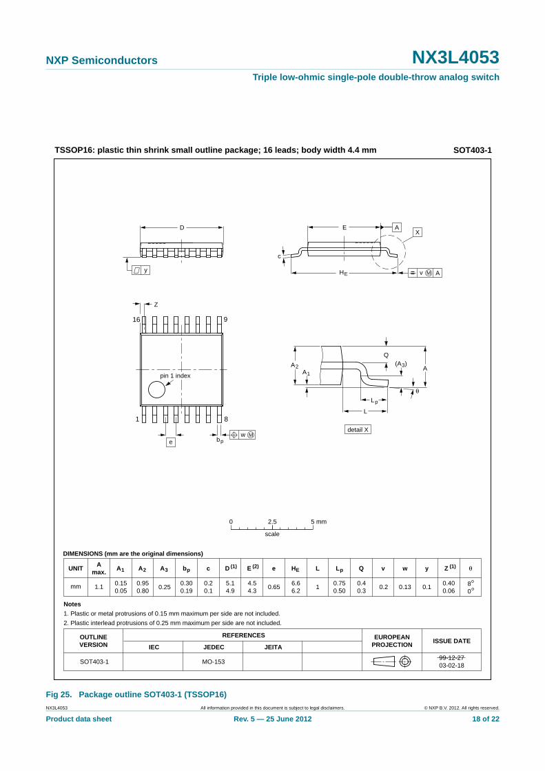
13. Package outline
Fig 24. Package outline SOT1039-2 (HXQFN16)
ReferencesOutlineversion
Europeanprojection Issue date
IEC JEDEC JEITA
SOT1039-2 - - -- - -
sot1039-2_po
10-07-2911-03-30
Unit
mmmaxnommin
0.5 0.05
0.000.127
3.13.02.9
1.951.851.75
3.13.02.9
0.5 1.50.400.350.30
0.1
A
Dimensions
HXQFN16: plastic thermal enhanced extremely thin quad flat package; no leads;16 terminals; body 3 x 3 x 0.5 mm SOT1039-2
A1 b
0.350.300.25
c D Dh E Eh
1.951.851.75
e e1 e2
1.5
L v
0.1
w
0.05
y
0.05
y1
0 1 2 mm
scale
terminal 1index area
B AD
E
C
yCy1
X
detail X
A
cA1
b
e2
e1
e
e
1/2 e
1/2 eAC Bv
Cw
terminal 1index area Dh
Eh
L
5 8
16 13
4
1
9
12
NX3L4053 All information provided in this document is subject to legal disclaimers. © NXP B.V. 2012. All rights reserved.
Product data sheet Rev. 5 — 25 June 2012 17 of 22
NXP Semiconductors NX3L4053Triple low-ohmic single-pole double-throw analog switch
Fig 25. Package outline SOT403-1 (TSSOP16)
UNIT A1 A2 A3 bp c D (1) E (2) (1)e HE L Lp Q Zywv θ
REFERENCESOUTLINEVERSION
EUROPEANPROJECTION ISSUE DATE
IEC JEDEC JEITA
mm 0.150.05
0.950.80
0.300.19
0.20.1
5.14.9
4.54.3
0.656.66.2
0.40.3
0.400.06
80
o
o0.13 0.10.21
DIMENSIONS (mm are the original dimensions)
Notes
1. Plastic or metal protrusions of 0.15 mm maximum per side are not included.
2. Plastic interlead protrusions of 0.25 mm maximum per side are not included.
0.750.50
SOT403-1 MO-15399-12-2703-02-18
w Mbp
D
Z
e
0.25
1 8
16 9
θ
AA1
A2
Lp
Q
detail X
L
(A )3
HE
E
c
v M A
XA
y
0 2.5 5 mm
scale
TSSOP16: plastic thin shrink small outline package; 16 leads; body width 4.4 mm SOT403-1
Amax.
1.1
pin 1 index
NX3L4053 All information provided in this document is subject to legal disclaimers. © NXP B.V. 2012. All rights reserved.
Product data sheet Rev. 5 — 25 June 2012 18 of 22
NXP Semiconductors NX3L4053Triple low-ohmic single-pole double-throw analog switch
14. Abbreviations
15. Revision history
Table 13. Abbreviations
Acronym Description
CDM Charged Device Model
CMOS Complementary Metal-Oxide Semiconductor
ESD ElectroStatic Discharge
HBM Human Body Model
MM Machine Model
PDA Personal Digital Assistant
Table 14. Revision history
Document ID Release date Data sheet status Change notice Supersedes
NX3L4053 v.5 20120625 Product data sheet - NX3L4053 v.4
Modifications: • For type number NX3L4053HR the sot code has changed to SOT1039-2.
NX3L4053 v.4 20111107 Product data sheet - NX3L4053 v.3
Modifications: • Legal pages updated.
NX3L4053 v.3 20101223 Product data sheet - NX3L4053 v.2
NX3L4053 v.2 20100811 Product data sheet - NX3L4053 v.1
NX3L4053 v.1 20100416 Product data sheet - -
NX3L4053 All information provided in this document is subject to legal disclaimers. © NXP B.V. 2012. All rights reserved.
Product data sheet Rev. 5 — 25 June 2012 19 of 22
NXP Semiconductors NX3L4053Triple low-ohmic single-pole double-throw analog switch
16. Legal information
16.1 Data sheet status
[1] Please consult the most recently issued document before initiating or completing a design.
[2] The term ‘short data sheet’ is explained in section “Definitions”.
[3] The product status of device(s) described in this document may have changed since this document was published and may differ in case of multiple devices. The latest product status information is available on the Internet at URL http://www.nxp.com.
16.2 Definitions
Draft — The document is a draft version only. The content is still under internal review and subject to formal approval, which may result in modifications or additions. NXP Semiconductors does not give any representations or warranties as to the accuracy or completeness of information included herein and shall have no liability for the consequences of use of such information.
Short data sheet — A short data sheet is an extract from a full data sheet with the same product type number(s) and title. A short data sheet is intended for quick reference only and should not be relied upon to contain detailed and full information. For detailed and full information see the relevant full data sheet, which is available on request via the local NXP Semiconductors sales office. In case of any inconsistency or conflict with the short data sheet, the full data sheet shall prevail.
Product specification — The information and data provided in a Product data sheet shall define the specification of the product as agreed between NXP Semiconductors and its customer, unless NXP Semiconductors and customer have explicitly agreed otherwise in writing. In no event however, shall an agreement be valid in which the NXP Semiconductors product is deemed to offer functions and qualities beyond those described in the Product data sheet.
16.3 Disclaimers
Limited warranty and liability — Information in this document is believed to be accurate and reliable. However, NXP Semiconductors does not give any representations or warranties, expressed or implied, as to the accuracy or completeness of such information and shall have no liability for the consequences of use of such information. NXP Semiconductors takes no responsibility for the content in this document if provided by an information source outside of NXP Semiconductors.
In no event shall NXP Semiconductors be liable for any indirect, incidental, punitive, special or consequential damages (including - without limitation - lost profits, lost savings, business interruption, costs related to the removal or replacement of any products or rework charges) whether or not such damages are based on tort (including negligence), warranty, breach of contract or any other legal theory.
Notwithstanding any damages that customer might incur for any reason whatsoever, NXP Semiconductors’ aggregate and cumulative liability towards customer for the products described herein shall be limited in accordance with the Terms and conditions of commercial sale of NXP Semiconductors.
Right to make changes — NXP Semiconductors reserves the right to make changes to information published in this document, including without limitation specifications and product descriptions, at any time and without notice. This document supersedes and replaces all information supplied prior to the publication hereof.
Suitability for use — NXP Semiconductors products are not designed, authorized or warranted to be suitable for use in life support, life-critical or safety-critical systems or equipment, nor in applications where failure or malfunction of an NXP Semiconductors product can reasonably be expected to result in personal injury, death or severe property or environmental damage. NXP Semiconductors and its suppliers accept no liability for inclusion and/or use of NXP Semiconductors products in such equipment or applications and therefore such inclusion and/or use is at the customer’s own risk.
Applications — Applications that are described herein for any of these products are for illustrative purposes only. NXP Semiconductors makes no representation or warranty that such applications will be suitable for the specified use without further testing or modification.
Customers are responsible for the design and operation of their applications and products using NXP Semiconductors products, and NXP Semiconductors accepts no liability for any assistance with applications or customer product design. It is customer’s sole responsibility to determine whether the NXP Semiconductors product is suitable and fit for the customer’s applications and products planned, as well as for the planned application and use of customer’s third party customer(s). Customers should provide appropriate design and operating safeguards to minimize the risks associated with their applications and products.
NXP Semiconductors does not accept any liability related to any default, damage, costs or problem which is based on any weakness or default in the customer’s applications or products, or the application or use by customer’s third party customer(s). Customer is responsible for doing all necessary testing for the customer’s applications and products using NXP Semiconductors products in order to avoid a default of the applications and the products or of the application or use by customer’s third party customer(s). NXP does not accept any liability in this respect.
Limiting values — Stress above one or more limiting values (as defined in the Absolute Maximum Ratings System of IEC 60134) will cause permanent damage to the device. Limiting values are stress ratings only and (proper) operation of the device at these or any other conditions above those given in the Recommended operating conditions section (if present) or the Characteristics sections of this document is not warranted. Constant or repeated exposure to limiting values will permanently and irreversibly affect the quality and reliability of the device.
Terms and conditions of commercial sale — NXP Semiconductors products are sold subject to the general terms and conditions of commercial sale, as published at http://www.nxp.com/profile/terms, unless otherwise agreed in a valid written individual agreement. In case an individual agreement is concluded only the terms and conditions of the respective agreement shall apply. NXP Semiconductors hereby expressly objects to applying the customer’s general terms and conditions with regard to the purchase of NXP Semiconductors products by customer.
No offer to sell or license — Nothing in this document may be interpreted or construed as an offer to sell products that is open for acceptance or the grant, conveyance or implication of any license under any copyrights, patents or other industrial or intellectual property rights.
Document status[1][2] Product status[3] Definition
Objective [short] data sheet Development This document contains data from the objective specification for product development.
Preliminary [short] data sheet Qualification This document contains data from the preliminary specification.
Product [short] data sheet Production This document contains the product specification.
NX3L4053 All information provided in this document is subject to legal disclaimers. © NXP B.V. 2012. All rights reserved.
Product data sheet Rev. 5 — 25 June 2012 20 of 22
NXP Semiconductors NX3L4053Triple low-ohmic single-pole double-throw analog switch
Export control — This document as well as the item(s) described herein may be subject to export control regulations. Export might require a prior authorization from competent authorities.
Non-automotive qualified products — Unless this data sheet expressly states that this specific NXP Semiconductors product is automotive qualified, the product is not suitable for automotive use. It is neither qualified nor tested in accordance with automotive testing or application requirements. NXP Semiconductors accepts no liability for inclusion and/or use of non-automotive qualified products in automotive equipment or applications.
In the event that customer uses the product for design-in and use in automotive applications to automotive specifications and standards, customer (a) shall use the product without NXP Semiconductors’ warranty of the product for such automotive applications, use and specifications, and (b) whenever customer uses the product for automotive applications beyond
NXP Semiconductors’ specifications such use shall be solely at customer’s own risk, and (c) customer fully indemnifies NXP Semiconductors for any liability, damages or failed product claims resulting from customer design and use of the product for automotive applications beyond NXP Semiconductors’ standard warranty and NXP Semiconductors’ product specifications.
Translations — A non-English (translated) version of a document is for reference only. The English version shall prevail in case of any discrepancy between the translated and English versions.
16.4 TrademarksNotice: All referenced brands, product names, service names and trademarks are the property of their respective owners.
17. Contact information
For more information, please visit: http://www.nxp.com
For sales office addresses, please send an email to: [email protected]
NX3L4053 All information provided in this document is subject to legal disclaimers. © NXP B.V. 2012. All rights reserved.
Product data sheet Rev. 5 — 25 June 2012 21 of 22
NXP Semiconductors NX3L4053Triple low-ohmic single-pole double-throw analog switch
18. Contents
1 General description . . . . . . . . . . . . . . . . . . . . . . 1
2 Features and benefits . . . . . . . . . . . . . . . . . . . . 1
3 Applications . . . . . . . . . . . . . . . . . . . . . . . . . . . . 2
4 Ordering information. . . . . . . . . . . . . . . . . . . . . 2
5 Marking . . . . . . . . . . . . . . . . . . . . . . . . . . . . . . . . 2
6 Functional diagram . . . . . . . . . . . . . . . . . . . . . . 3
7 Pinning information. . . . . . . . . . . . . . . . . . . . . . 37.1 Pinning . . . . . . . . . . . . . . . . . . . . . . . . . . . . . . . 37.2 Pin description . . . . . . . . . . . . . . . . . . . . . . . . . 4
8 Functional description . . . . . . . . . . . . . . . . . . . 4
9 Limiting values. . . . . . . . . . . . . . . . . . . . . . . . . . 4
10 Recommended operating conditions. . . . . . . . 5
11 Static characteristics. . . . . . . . . . . . . . . . . . . . . 511.1 Test circuits . . . . . . . . . . . . . . . . . . . . . . . . . . . . 611.2 ON resistance. . . . . . . . . . . . . . . . . . . . . . . . . . 711.3 ON resistance test circuit and graphs. . . . . . . . 8
12 Dynamic characteristics . . . . . . . . . . . . . . . . . 1012.1 Waveform and test circuits . . . . . . . . . . . . . . . 1112.2 Additional dynamic characteristics . . . . . . . . . 1312.3 Test circuits . . . . . . . . . . . . . . . . . . . . . . . . . . . 14
13 Package outline . . . . . . . . . . . . . . . . . . . . . . . . 17
14 Abbreviations. . . . . . . . . . . . . . . . . . . . . . . . . . 19
15 Revision history. . . . . . . . . . . . . . . . . . . . . . . . 19
16 Legal information. . . . . . . . . . . . . . . . . . . . . . . 2016.1 Data sheet status . . . . . . . . . . . . . . . . . . . . . . 2016.2 Definitions. . . . . . . . . . . . . . . . . . . . . . . . . . . . 2016.3 Disclaimers . . . . . . . . . . . . . . . . . . . . . . . . . . . 2016.4 Trademarks. . . . . . . . . . . . . . . . . . . . . . . . . . . 21
17 Contact information. . . . . . . . . . . . . . . . . . . . . 21
18 Contents . . . . . . . . . . . . . . . . . . . . . . . . . . . . . . 22
© NXP B.V. 2012. All rights reserved.
For more information, please visit: http://www.nxp.comFor sales office addresses, please send an email to: [email protected]
Date of release: 25 June 2012
Document identifier: NX3L4053
Please be aware that important notices concerning this document and the product(s)described herein, have been included in section ‘Legal information’.
![NX3L2267 Low-ohmic dual single-pole double-throw analog ...11.2 ON resistance Table 8. ON resistance [1] Typical values are measured at Tamb = 25 C. [2] Measured at identical VCC,](https://img.pdfslide.net/doc/110x75/611d967399fb0b7671422b08/nx3l2267-low-ohmic-dual-single-pole-double-throw-analog-112-on-resistance-table.jpg)