Embed Size (px)
Citation preview
UM11225NXP SE05x T=1 Over I2C SpecificationRev. 1.1 — 8 January 2020 User manual
COMPANY PUBLIC
Document informationInformation Content
Keywords I2C T=1 ISO7816 SE05x
Abstract Specification for the data link layer protocol T=1 over I2C on the SE05x
NXP Semiconductors UM11225NXP SE05x T=1 Over I2C Specification
UM11225 All information provided in this document is subject to legal disclaimers. © NXP B.V. 2020. All rights reserved.
User manual Rev. 1.1 — 8 January 2020COMPANY PUBLIC 2 / 25
1 Introduction
T=1 is a peer to peer, half duplex transmission protocol defined in ISO/IEC 7816-3. T=1protocol usage is very common in the smart card domain. This document specifies howISO/IEC 7816-3 T=1 protocol shall be used to transfer APDUs between a hosting device(HD) and a Secure Element (SE) using serial physical interfaces based on I2C .
In view of the OSI protocol stack the serial physical interface I2C , shall serve as physicallayers. A customized ISO/IEC 7816-3 T=1 protocol shall be used as data link layer.
Table 1. Revision historyRev Date Description
Rev 1.1 20200108 Modifications:• Added definition for DPWT (Power Wake-Up Time)• Updated figure Figure 2• Updated figure Figure 6 with STOP condition and MPOT• Updated figure Figure 9• Updated figure Figure 11• Update table Table 14 to remove IRQCT and SEAL (not supported by this product)• Updated chapter Section 2 add further statement to first item of the list.• Updated chapter Section 2.1.1.1 to remove statement about multiple NAD values• Updated chapter Section 2.1.1.2.3 to include further explanation on the Interface soft reset
request and SE Chip reset request S-Block and add a new statement for WTX request• Updated chapter Section 2.4.2• Updated chapter Section 3 to update list of characteristics for I2C• Updated chapter Section 3.1.1 to include statement that if I2C bus is free both lines SDA and
SCL shall be HIGH• Added chapter SE I2C Default Values Section 3.1.1.4
NXP Semiconductors UM11225NXP SE05x T=1 Over I2C Specification
UM11225 All information provided in this document is subject to legal disclaimers. © NXP B.V. 2020. All rights reserved.
User manual Rev. 1.1 — 8 January 2020COMPANY PUBLIC 3 / 25
2 Data Link Layer (T=1)
This specification uses a Data Link Layer based on T=1 half duplex communicationprotocol as defined in ISO/IEC 7816-3. Proprietary extensions are added to ISO/IEC7816-3 T=1 protocol to improve performance and to support additional features.
The main characteristics of this transmission protocol are the following:
• The transmission protocol starts with a first block transmitted by the hosting device(HD); it continues with alternating the right to transmit a block. Consequently, the HDshall always read the response of a previous request before issuing a new request toensure the command and response sequence is always kept.
• A block is the smallest data unit that can be exchanged. A block may be used toconvey:– Application data transparent to the transmission protocol.– Transmission control data including transmission error handling.
• The block structure allows checking the received block before processing the conveyeddata.
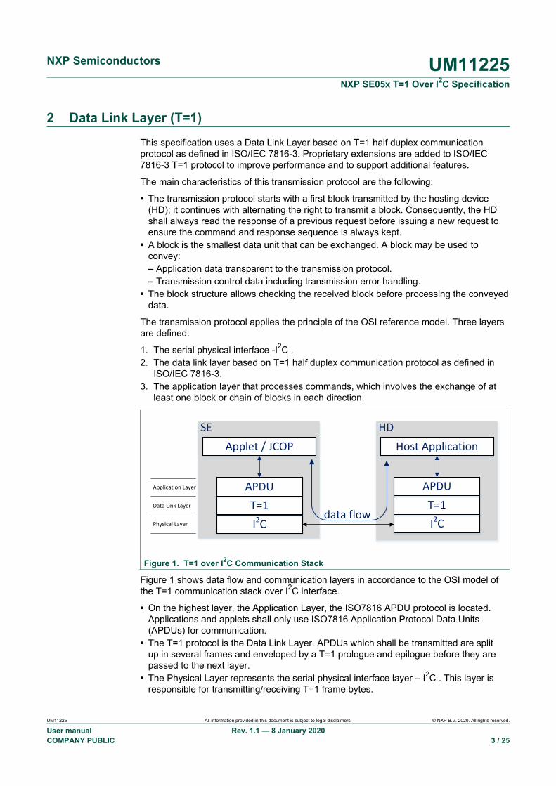
The transmission protocol applies the principle of the OSI reference model. Three layersare defined:
1. The serial physical interface -I2C .2. The data link layer based on T=1 half duplex communication protocol as defined in
ISO/IEC 7816-3.3. The application layer that processes commands, which involves the exchange of at
least one block or chain of blocks in each direction.
I2CT=1
APDU
I2CT=1
APDU
Host ApplicationApplet / JCOPSE HD
data flowPhysical Layer
Data Link Layer
Application Layer
Figure 1. T=1 over I2C Communication Stack
Figure 1 shows data flow and communication layers in accordance to the OSI model ofthe T=1 communication stack over I2C interface.
• On the highest layer, the Application Layer, the ISO7816 APDU protocol is located.Applications and applets shall only use ISO7816 Application Protocol Data Units(APDUs) for communication.
• The T=1 protocol is the Data Link Layer. APDUs which shall be transmitted are splitup in several frames and enveloped by a T=1 prologue and epilogue before they arepassed to the next layer.
• The Physical Layer represents the serial physical interface layer – I2C . This layer isresponsible for transmitting/receiving T=1 frame bytes.
NXP Semiconductors UM11225NXP SE05x T=1 Over I2C Specification
UM11225 All information provided in this document is subject to legal disclaimers. © NXP B.V. 2020. All rights reserved.
User manual Rev. 1.1 — 8 January 2020COMPANY PUBLIC 4 / 25
2.1 T=1 Block Frame Format
The T=1 block frame consists of three fields as shown in Table 2.
1. Prologue Field consists ofa. Node Address byte (NAD)b. Protocol Control Byte (PCB)c. Information Field Length (LEN)
2. Information Field (INF) consists of zero to LEN bytes. This field shall be present onlyif LEN is non-zero
3. Epilogue Field conveys the error detection code of the block. Two bytes cyclicredundancy code (CRC) is used for error detection as defined in [1].
Table 2. T=1 Frame FormatPrologue field (mandatory) Information field (optional) Epilogue field (mandatory)
NAD (1 byte) PCB (1 byte) LEN (1 byte) INF (0 to LEN bytes) CRC16 (2 bytes)
2.1.1 Prologue Field
One-byte LEN field is used in a 3-byte prologue and is used for blocks with 0 to 0xFEbytes in information field. Table 3 shows the 3-byte prologue field format.
Table 3. 3-Byte Prologue3-byte Prologue field
NAD (1 byte) PCB (1 byte) LEN (1 byte)
2.1.1.1 Node Address Byte (NAD)
The node address byte (NAD) identifies the source and the intended destination of theblock. Bits 1 to 4 encode the source node address (SAD) and bits 5 to 8 encode thedestination node address (DAD). Values '0xFF' and '0x00' are invalid for NAD. DAD andSAD shall never have the same value.
Table 4. NAD FormatDestination address (DAD) Source address (SAD)
8 – 5 4 – 1
Table 5 lists proposed SAD and DAD values.
Table 5. SAD/DAD valuesCommunication Direction DAD SAD NAD value
HD to SE 0x5 0xA 0x5A
SE to HD 0xA 0x5 0xA5
2.1.1.2 Protocol Control Byte (PCB)
The protocol control byte (PCB) conveys information required to control transmission.PCB indicates the block frame type and defines whether the block is an I-Block, a R-Block or a S-Block.
• An information block (I-Block) is used to convey information for use by the applicationlayer.
NXP Semiconductors UM11225NXP SE05x T=1 Over I2C Specification
UM11225 All information provided in this document is subject to legal disclaimers. © NXP B.V. 2020. All rights reserved.
User manual Rev. 1.1 — 8 January 2020COMPANY PUBLIC 5 / 25
• A receive ready block (R-Block) is used to convey a positive or negativeacknowledgement.
• A supervisory block (S-Block) is used to exchange control information between the HDand the SE.
2.1.1.2.1 Coding Of I-Block PCB
Bit-8 of the PCB is set to 0 for an I-Block.
• Bit-7 encodes the send-sequence number denoted N(S). N(S) alternates between 1and 0.
• Bit-6 is the more-data bit denoted M-bit. M-bit is used for I-Block chaining.• Bits 5 to 1 are reserved for future use and shall be set to 0.
Table 6. Coding of I-Block PCBBit-8 Bit-7 Bit-6 Bit-5 Bit-4 Bit-3 Bit-2 Bit-1
0 N(S) M 0 0 0 0 0
The chaining function allows the HD or the SE to transmit information (application data)longer than IFSC or IFSD. If the HD or the SE must transmit information longer thanIFSC or IFSD respectively, it shall divide the information into pieces, each with lengthless than or equal to IFSC or IFSD and shall transmit each piece in a block using thechaining function.
The M-bit in PCB controls the chaining of I-Blocks. The value of the M-bit indicates thestate of the I-Block.
• If M = 1, then the I-Block is chained to the next block, which shall be an I-Block.• If M = 0, then the I-Block is not chained to the next block.
If the receiver correctly receives a more-data I-Block, then it shall transmit R(N(R)),where N(R) is set to N(S) of the expected I-Block.
2.1.1.2.2 Coding of R-Block PCB
Bits 8 and 7 of the PCB are set to 10b for an R-Block.
• Bit-5 encodes the expected sequence number denoted N(R).• Bits 1 and 2 encode the error code. Refer to Table 8 for the supported error codes• Remaining bits are reserved for future use and shall be set to 0.
Table 7. Coding of R-Block PCBBit-8 Bit-7 Bit-6 Bit-5 Bit-4 Bit-3 Bit-2 Bit-1
1 0 0 N(R) 0 0 Error code
Table 8. R-Block Error codesBit-2 Bit-1 Error definition
0 0 Error-free acknowledgement
0 1 CRC error
1 0 Other error
R-Block is used to:
NXP Semiconductors UM11225NXP SE05x T=1 Over I2C Specification
UM11225 All information provided in this document is subject to legal disclaimers. © NXP B.V. 2020. All rights reserved.
User manual Rev. 1.1 — 8 January 2020COMPANY PUBLIC 6 / 25
• Indicate error and request the sender to re-transmit the last block• Acknowledge error-free reception of I-Block in case of chaining
2.1.1.2.3 Coding of S-Block PCB
Bits 8 and 7 of the PCB are set to 11b for an S-Block. Remaining bits are used to encodeS-Block request/response commands as listed in Table 10.
Table 9. Generic S-Block CodingBit-8 Bit-7 Bit-6 Bit-5 Bit-4 Bit-3 Bit-2 Bit-1
1 1 Request/Response command
Table 10. Coding of S-Block PCBS-Block Command Bits 1 to 6 INF Description
RESYNC request 000000b Command to re-synchronize and reset I-Blocksequence number to zero
RESYNC response 100000bAbsent. LEN = 0
Response command to acknowledge RESYNCrequest
IFS request 000001bCommand to request IFS length change. INFfield holds the requested IFS size. Refer toSection 2.1.2.1 for details
IFS response 100001b
IFS sizeResponse command to acknowledge IFSrequest
ABORT request 000010b Command to request chain abortion
ABORT response 100010bAbsent. LEN = 0 Response command to acknowledge ABORT
request
WTX request 000011b Command to request Waiting Time extension
WTX response 100011binteger multiplier
of the BWT Response command toacknowledge WTX request
Interface soft reset request 001111b Absent. LEN = 0 Command to request for a soft reset of the logicalconnection.
Interface soft reset response101111b
ATR bytesResponse command to acknowledge interfacereset request. Refer to section Section 2.2 fordetails
End of APDU session request 000101b Command to indicate end of APDU session.
End of APDU session response 100101bAbsent. LEN = 0
Response command to acknowledge end ofAPDU command. SE shall reset the protocolcontext and initiate power saving sequence aftersending the command response.
SE Chip reset request 000110b Command to request reset of SE.
SE Chip reset response 100110bAbsent. LEN = 0 Response command to acknowledge SE chip
reset command. SE shall do a power reset aftersending the command response.
Get ATR request 000111b Absent. LEN = 0 Command to retrieve ATR bytes withoutresetting SE
NXP Semiconductors UM11225NXP SE05x T=1 Over I2C Specification
UM11225 All information provided in this document is subject to legal disclaimers. © NXP B.V. 2020. All rights reserved.
User manual Rev. 1.1 — 8 January 2020COMPANY PUBLIC 7 / 25
S-Block Command Bits 1 to 6 INF Description
Get ATR response 100111b ATR bytes Response command to acknowledge Get ATRrequest. ATR bytes are send in INF field
Interface soft reset request S-Block command shall reset both protocol context andSE context with respect to the logical connection. SE shall send the command responsewith ATR bytes in INF field once the context reset is complete. HD shall not send thiscommand as a response to WTX request. On soft reset, SE shall discard any pendingresponse block on the logical connection. After Host has send the Interface soft resetrequest S-Block Host must ensure that for DMPOT SCL and SDA lines are in the defaultstate HIGH.
HD shall use End of APDU session request S-Block command to indicate end ofAPDU session on the logical connection. SE shall reset the protocol context of the logicalconnection and may initiate power saving sequence after sending response to thiscommand. SE shall wake up automatically if HD sends a T=1 block.
SE Chip reset request S-Block command shall reset SE chip. SE shall do self-resetonce the response command is send to the HD. After Host has send the SE Chip resetrequest S-Block Host must ensure that for DPWT SCL and SDA lines are in the defaultstate HIGH.
HD shall always respond to a WTX request with a WTX response.
2.1.1.3 Information Field Length (LEN)
The Information Field Length (LEN) byte(s) encodes the number of bytes in theinformation field of the block.
• The value ‘00’ encodes zero: INF is absent.• One-byte LEN shall be used in Prologue field if the information field size is less than
0xFF bytes.
2.1.2 Information Field (INF)
The contents of the information field bytes depend upon the block type.
Table 11. Block TypesBlock type Information field usage
I-Block Application data (C-APDU/R-APDU)
R-Block Absent
S-Block Refer to Table 10 for details
2.1.2.1 Information Field Size (IFS)
The Information Field Size (IFS) defines the maximum size of information field (INF) thata block can hold.
• IFSC defines the IFS of the SE• IFSD defines the IFS of the HD
This protocol uses the same value for both IFSC and IFSD and both values are always insync. ATR includes the maximum IFSC value of the SE.
NXP Semiconductors UM11225NXP SE05x T=1 Over I2C Specification
UM11225 All information provided in this document is subject to legal disclaimers. © NXP B.V. 2020. All rights reserved.
User manual Rev. 1.1 — 8 January 2020COMPANY PUBLIC 8 / 25
SE shall use the maximum IFS size indicated in ATR on init. HD may use IFS requestS-Block command to reduce the IFS size. SE shall acknowledge the request by IFSresponse S-Block command if the requested IFS size can be supported. SE shall resetthe IFS to maximum value on soft reset.
IFS size of each logical connection shall be maintained separately. Soft reset commandsend on one logical connection shall reset the IFS of that logical connection only.
2.1.3 Epilogue Field (CRC)
The epilogue field conveys the error detection code of the block. Cyclic redundancy code(CRC) is used for error detection.
CRC shall be computed for all bytes in Prologue and INF fields.
2.2 Answer to Reset (ATR)
SE shall return ATR bytes as a response to Soft Reset request or Get ATR request S-Block command. INF bytes of interface soft reset/Get ATR S-Block response commandshall hold the ATR bytes.
2.2.1 ATR – Common Structure
This section describes the common structure of the ATR, irrespective of the PhysicalLayer that is used.
Table 12. ATR – Common StructureName Length Description
PVER
1 Protocol Version.This version of the specification defines version '01' of the protocol. Higher versionsshall be backward compatible with lower versions. Lower versions may miss some newcapabilities of higher versions.
VID 5 Vendor ID according to [7816-4]
Length ofDLLP
1 Length of Data Link Layer Parameters
DLLP Var. Data Link Layer Parameters: See Table 13
PLID 1 Physical Layer ID (always I2C so fixed to 2)
Length of PLP 1 Length of Physical Layer Parameters
PLP Var. Physical Layer Parameters: See Table 14
Length of HB 1 Length of Historical Bytes
HB Var. Historical Bytes
2.2.2 ATR – Specific Parameters for Data Link Layer
This section describes the parameters provided by the ATR for the Data Link Layer.
Table 13. ATR – Specific Parameters for Data Link LayerName Length Description
BWT 2 Block Waiting Time (in ms)
IFSC 2 Maximum Information Field Size of the SE (in bytes)
NXP Semiconductors UM11225NXP SE05x T=1 Over I2C Specification
UM11225 All information provided in this document is subject to legal disclaimers. © NXP B.V. 2020. All rights reserved.
User manual Rev. 1.1 — 8 January 2020COMPANY PUBLIC 9 / 25
2.2.3 ATR – Specific Parameters for I2C Physical Layer
This section describes the parameters provided by the ATR when the I2C Physical Layeris used.
Table 14. ATR – Specific Parameters for I2C Physical LayerName Length Description
MCF 2 Maximal I2C Clock Frequency at which the SE may operate (in kHz)
Configuration 1 Method for SE Data Available that shall be used by the HD to detect that response datamay be read from the SE:• b1-b3: RFUSupport of the I2C High Speed Mode :• b4 = 0: HS mode not supported• b4 = 1: HS mode supported
MPOT 1 Minimum Polling Time (conditional to Polling Mode support) (in ms)
RFU 1 Not used for this product
RFU 2 Not used for this product
SEGT 2 Secure Element Guard Time (in µs)
WUT 2 Wake-Up Time (in µs): when receiving a Wake-Up Byte, time after which the SE is ready toreceive a command.
2.3 Rules for Error-Free Operation
To ensure error free operation, this protocol shall follow below rules in addition to therules listed in section 11.6.2 of [1].
2.3.1 Initialization
SE shall be in Receive state after power-on boot. The HD shall transmit the first block.First block shall be either an I-Block with N(S) = 0 denoted I(0, M), or an S-Block.
SE shall be in Send state after receiving S(Interface soft reset request) to send out theATR, but shall reset the protocol context.
Note: It is recommended that HD should use S(Interface soft reset request) after power-on boot to ensure HD and SE are synchronized.
2.3.2 Processing
SE shall enter Process state on receiving the command block from the HD and shall exitProcess state and go to Send state once the command is processed. When response isread out by the HD, SE shall go to Receive state again.
2.3.3 Acknowledgement
I-Blocks are acknowledged by sending the next I-Block.
Without chaining or at the last block of a chain, I(Na(S), 0) transmitted by A is implicitlyacknowledged by I(Nb(S), M) transmitted by B.
With chaining, I(Na(S), 1) transmitted by A is acknowledged by R(Nb(R)) transmitted byB, with Nb(R) indicating the send-sequence number of the next expected block.
NXP Semiconductors UM11225NXP SE05x T=1 Over I2C Specification
UM11225 All information provided in this document is subject to legal disclaimers. © NXP B.V. 2020. All rights reserved.
User manual Rev. 1.1 — 8 January 2020COMPANY PUBLIC 10 / 25
2.3.4 Waiting Time Extension
If the SE requires more than BWT to process the previously received command block,it shall transmit S(WTX request) S-Block command. The HD shall acknowledge bysending S(WTX response).The new processing time starts at the leading edge of the lastcharacter of S(WTX response).
SE shall transmit S(WTX request) for both I-Block and S-Block commands if theprocessing of the command requires more than BWT.
2.4 Error handling
This protocol shall follow below rules to handle errors in addition to the error handlingrules listed in section 11.6.3 of [1].
2.4.1 Re-transmission
In case of a transmission error, where the HD either
• fails to receive an error-free block from SE, or• repeatedly receives an R-Block from SE.
HD shall make a maximum of ten further attempts in succession by sending an R-Blockto the SE or retransmitting the previously block.
HD shall transmit S(Interface soft reset request) after the maximum of retransmissionattempts.
2.4.2 Error Recovery
If the SE in Send state cannot send the complete command response block to the HD,because HD sends a new command block, before reading complete command responseblock, SE shall go to Receive state to receive the new command block. Commandresponse block shall be discarded. In this case SE behaves as if a S(Interface soft resetrequest) has been received..
NXP Semiconductors UM11225NXP SE05x T=1 Over I2C Specification
UM11225 All information provided in this document is subject to legal disclaimers. © NXP B.V. 2020. All rights reserved.
User manual Rev. 1.1 — 8 January 2020COMPANY PUBLIC 11 / 25
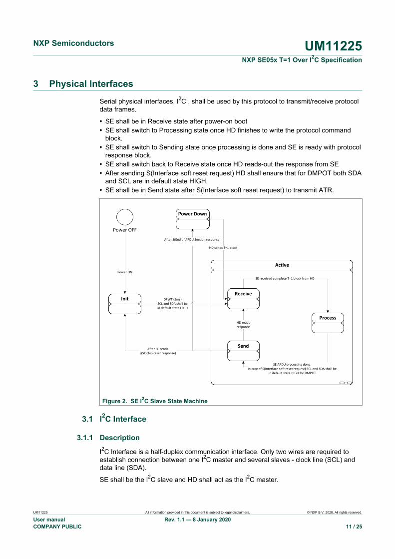
3 Physical Interfaces
Serial physical interfaces, I2C , shall be used by this protocol to transmit/receive protocoldata frames.
• SE shall be in Receive state after power-on boot• SE shall switch to Processing state once HD finishes to write the protocol command
block.• SE shall switch to Sending state once processing is done and SE is ready with protocol
response block.• SE shall switch back to Receive state once HD reads-out the response from SE• After sending S(Interface soft reset request) HD shall ensure that for DMPOT both SDA
and SCL are in default state HIGH.• SE shall be in Send state after S(Interface soft reset request) to transmit ATR.
Power OFF
InitReceive
Send
Process
DPWT (5ms)SCL and SDA shall be in default state HIGH
SE received complete T=1 block from HD
SE APDU processing done. In case of S(Interface soft reset request) SCL and SDA shall be
in default state HIGH for DMPOT
Power ON
HD reads response
Active
After SE sends S(SE chip reset response)
Power Down
After S(End of APDU Session response)
HD sends T=1 block
Figure 2. SE I2C Slave State Machine
3.1 I2C Interface
3.1.1 Description
I2C Interface is a half-duplex communication interface. Only two wires are required toestablish connection between one I2C master and several slaves - clock line (SCL) anddata line (SDA).
SE shall be the I2C slave and HD shall act as the I2C master.
NXP Semiconductors UM11225NXP SE05x T=1 Over I2C Specification
UM11225 All information provided in this document is subject to legal disclaimers. © NXP B.V. 2020. All rights reserved.
User manual Rev. 1.1 — 8 January 2020COMPANY PUBLIC 12 / 25
I2C Master(HD)
I2C Slave(SE)
SCL
SDA
SCL
SDA
Figure 3. Simplified I2C Schematics
Note: When the bus is free or idle, both lines SCL and SDA shall be HIGH.
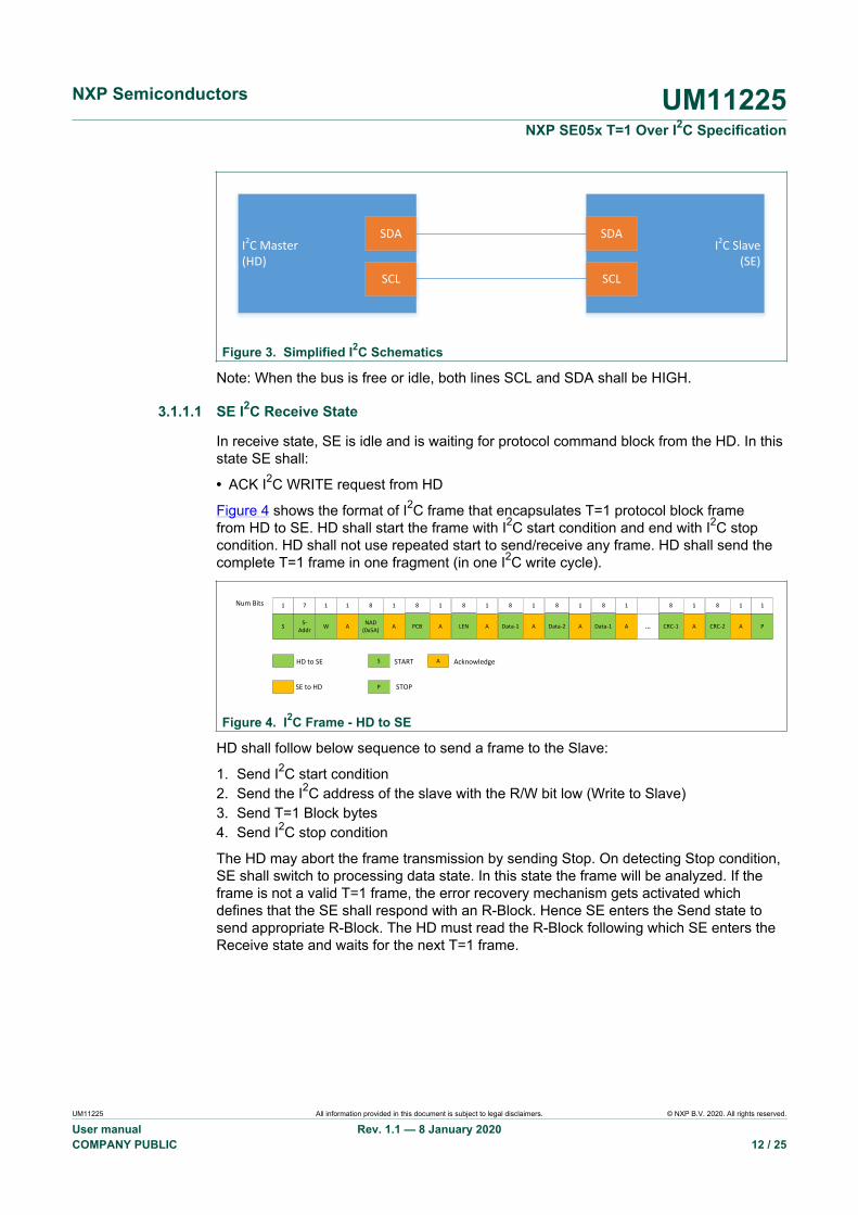
3.1.1.1 SE I2C Receive State
In receive state, SE is idle and is waiting for protocol command block from the HD. In thisstate SE shall:
• ACK I2C WRITE request from HD
Figure 4 shows the format of I2C frame that encapsulates T=1 protocol block framefrom HD to SE. HD shall start the frame with I2C start condition and end with I2C stopcondition. HD shall not use repeated start to send/receive any frame. HD shall send thecomplete T=1 frame in one fragment (in one I2C write cycle).
1
S
Num Bits 7
S-Addr
1
W
1
A
8
NAD (0x5A)
1
A
8
PCB
1
A
8
LEN
1
A
8
Data-1
1
A
8
Data-2
1
A
8
Data-1
1
A
8
CRC-1
1
A...
8
CRC-2
1
A
1
P
HD to SE
SE to HD
S
P
START
STOP
A Acknowledge
Figure 4. I2C Frame - HD to SE
HD shall follow below sequence to send a frame to the Slave:
1. Send I2C start condition2. Send the I2C address of the slave with the R/W bit low (Write to Slave)3. Send T=1 Block bytes4. Send I2C stop condition
The HD may abort the frame transmission by sending Stop. On detecting Stop condition,SE shall switch to processing data state. In this state the frame will be analyzed. If theframe is not a valid T=1 frame, the error recovery mechanism gets activated whichdefines that the SE shall respond with an R-Block. Hence SE enters the Send state tosend appropriate R-Block. The HD must read the R-Block following which SE enters theReceive state and waits for the next T=1 frame.
NXP Semiconductors UM11225NXP SE05x T=1 Over I2C Specification
UM11225 All information provided in this document is subject to legal disclaimers. © NXP B.V. 2020. All rights reserved.
User manual Rev. 1.1 — 8 January 2020COMPANY PUBLIC 13 / 25
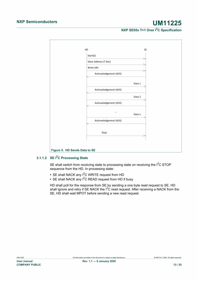
HD SE
Start(S)
Slave Address (7 bits)
Write (W)
Acknowledgement (ACK)
Acknowledgement (ACK)
Data 1
Acknowledgement (ACK)
Data 2
Stop
Data n
Acknowledgement (ACK)
...
Figure 5. HD Sends Data to SE
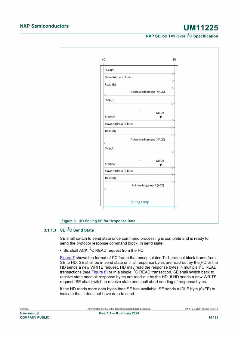
3.1.1.2 SE I2C Processing State
SE shall switch from receiving state to processing state on receiving the I2C STOPsequence from the HD. In processing state:
• SE shall NACK any I2C WRITE request from HD• SE shall NACK any I2C READ request from HD if busy
HD shall poll for the response from SE by sending a one byte read request to SE. HDshall ignore and retry if SE NACK the I2C read request. After receiving a NACK from theSE, HD shall wait MPOT before sending a new read request.
NXP Semiconductors UM11225NXP SE05x T=1 Over I2C Specification
UM11225 All information provided in this document is subject to legal disclaimers. © NXP B.V. 2020. All rights reserved.
User manual Rev. 1.1 — 8 January 2020COMPANY PUBLIC 14 / 25
HD SE
Start(S)
Slave Address (7 bits)
Read (R)
Acknowledgement (NACK)
Polling Loop
Start(S)
Slave Address (7 bits)
Read (R)
Acknowledgement (NACK)
Start(S)
Slave Address (7 bits)
Read (R)
Acknowledgement (ACK)
...
...
Stop(P)
Stop(P)
MPOT
MPOT
Figure 6. HD Polling SE for Response Data
3.1.1.3 SE I2C Send State
SE shall switch to send state once command processing is complete and is ready tosend the protocol response command block. In send state:
• SE shall ACK I2C READ request from the HD.
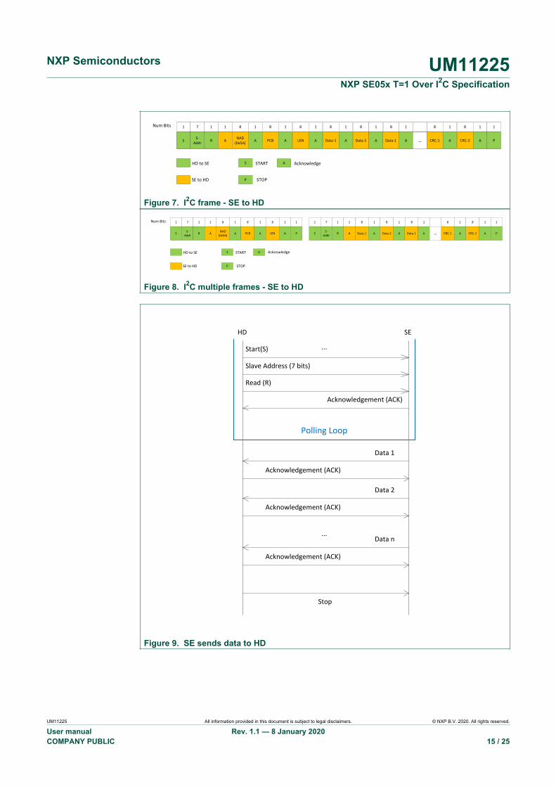
Figure 7 shows the format of I2C frame that encapsulates T=1 protocol block frame fromSE to HD. SE shall be in send state until all response bytes are read-out by the HD or theHD sends a new WRITE request. HD may read the response bytes in multiple I2C READtransactions (see Figure 8) or in a single I2C READ transaction. SE shall switch back toreceive state once all response bytes are read-out by the HD. If HD sends a new WRITErequest, SE shall switch to receive state and shall abort sending of response bytes.
If the HD reads more data bytes than SE has available, SE sends a IDLE byte (0xFF) toindicate that it does not have data to send.
NXP Semiconductors UM11225NXP SE05x T=1 Over I2C Specification
UM11225 All information provided in this document is subject to legal disclaimers. © NXP B.V. 2020. All rights reserved.
User manual Rev. 1.1 — 8 January 2020COMPANY PUBLIC 15 / 25
1
S
Num Bits 7
S-Addr
1
R
1
A
8
NAD (0x5A)
1
A
8
PCB
1
A
8
LEN
1
A
8
Data-1
1
A
8
Data-2
1
A
8
Data-1
1
A
8
CRC-1
1
A...
8
CRC-2
1
A
1
P
HD to SE
SE to HD
S
P
START
STOP
A Acknowledge
Figure 7. I2C frame - SE to HD
1
S
Num Bits 7
S-Addr
1
R
1
A
8
NAD (0x5A)
1
A
8
PCB
1
A
8
LEN
1
A
8
Data-1
1
A
8
Data-2
1
A
8
Data-1
1
A
8
CRC-1
1
A...
8
CRC-2
1
A
1
P
HD to SE
SE to HD
S
P
START
STOP
A Acknowledge
1
P
1
S
7
S-Addr
1
R
1
A
Figure 8. I2C multiple frames - SE to HD
HD SE
Start(S)
Slave Address (7 bits)
Read (R)
Acknowledgement (ACK)
Acknowledgement (ACK)
Data 1
Acknowledgement (ACK)
Data 2
Stop
Data n
Acknowledgement (ACK)
Polling Loop
...
...
Figure 9. SE sends data to HD
NXP Semiconductors UM11225NXP SE05x T=1 Over I2C Specification
UM11225 All information provided in this document is subject to legal disclaimers. © NXP B.V. 2020. All rights reserved.
User manual Rev. 1.1 — 8 January 2020COMPANY PUBLIC 16 / 25
HD SE
Start(S)
Slave Address (7 bits)
Read (R)
ACK
ACK
NAD
ACK
PCB
Stop
LEN
NACK
...
Start(S)
Slave Address (7 bits)
Read (R)
ACK
ACK
Data 0
ACK
Data 1
Stop
Data LEN-1
NACK
...
Figure 10. I2C multiple frames - SE to HD
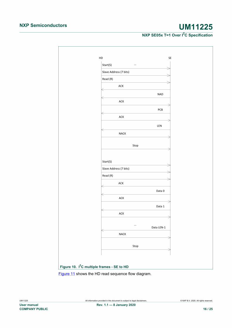
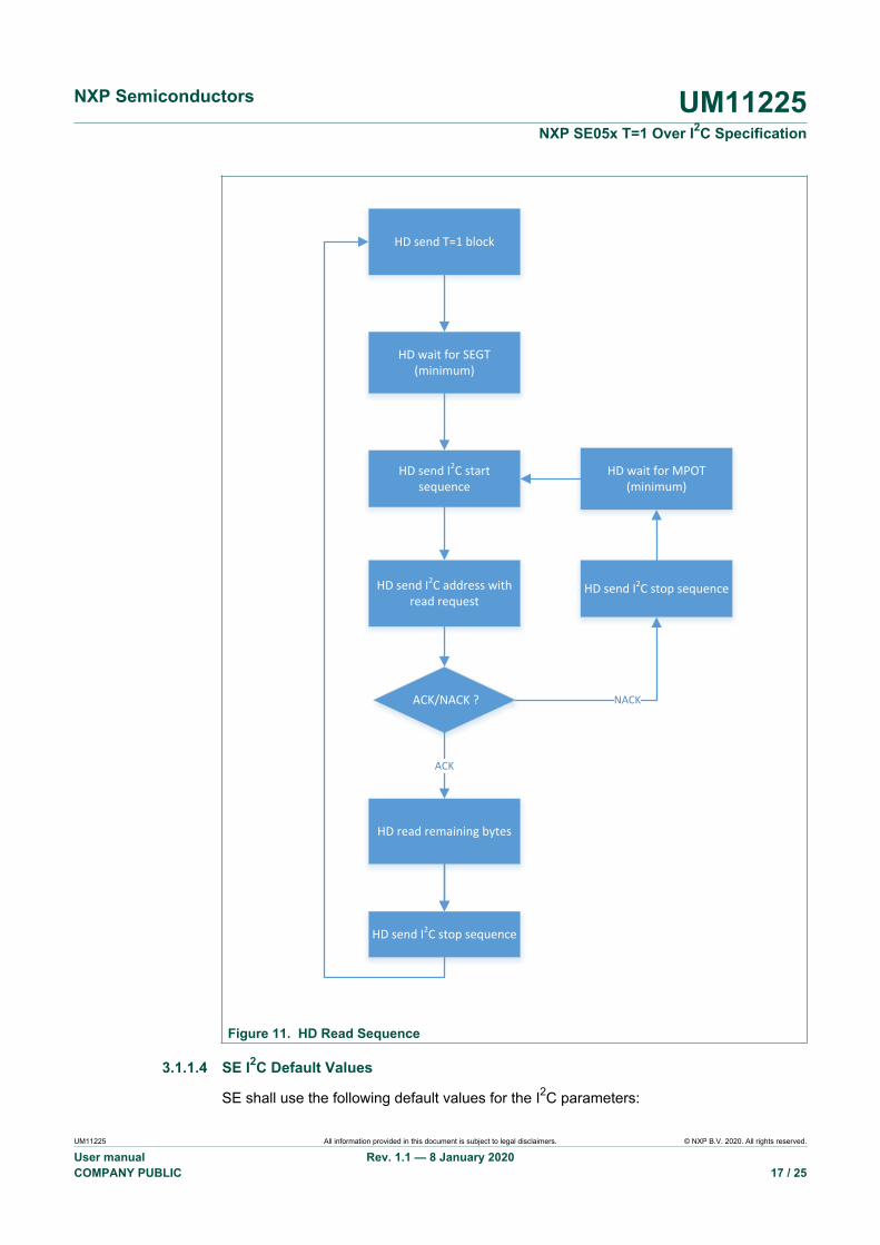
Figure 11 shows the HD read sequence flow diagram.
NXP Semiconductors UM11225NXP SE05x T=1 Over I2C Specification
UM11225 All information provided in this document is subject to legal disclaimers. © NXP B.V. 2020. All rights reserved.
User manual Rev. 1.1 — 8 January 2020COMPANY PUBLIC 17 / 25
HD send T=1 block
HD wait for SEGT (minimum)
HD send I2C start sequence
HD send I2C stop sequence
HD send I2C address with read request
ACK/NACK ?
HD read remaining bytes
HD send I2C stop sequence
NACK
ACK
HD wait for MPOT (minimum)
Figure 11. HD Read Sequence
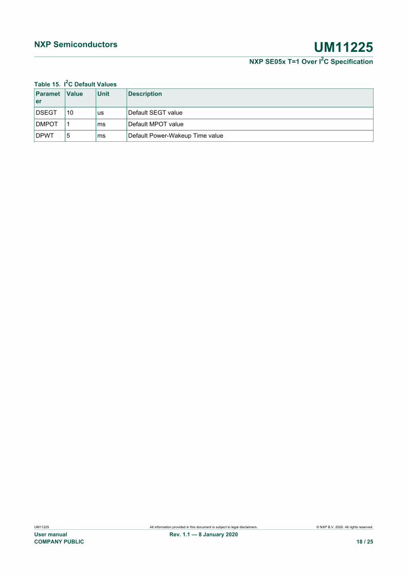
3.1.1.4 SE I2C Default Values
SE shall use the following default values for the I2C parameters:
NXP Semiconductors UM11225NXP SE05x T=1 Over I2C Specification
UM11225 All information provided in this document is subject to legal disclaimers. © NXP B.V. 2020. All rights reserved.
User manual Rev. 1.1 — 8 January 2020COMPANY PUBLIC 18 / 25
Table 15. I2C Default ValuesParameter
Value Unit Description
DSEGT 10 us Default SEGT value
DMPOT 1 ms Default MPOT value
DPWT 5 ms Default Power-Wakeup Time value
NXP Semiconductors UM11225NXP SE05x T=1 Over I2C Specification
UM11225 All information provided in this document is subject to legal disclaimers. © NXP B.V. 2020. All rights reserved.
User manual Rev. 1.1 — 8 January 2020COMPANY PUBLIC 19 / 25
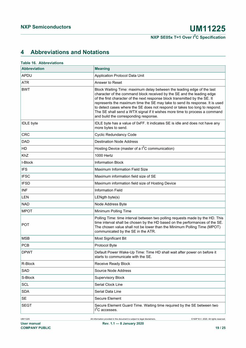
4 Abbreviations and NotationsTable 16. AbbreviationsAbbreviation Meaning
APDU Application Protocol Data Unit
ATR Answer to Reset
BWT Block Waiting Time: maximum delay between the leading edge of the lastcharacter of the command block received by the SE and the leading edgeof the first character of the next response block transmitted by the SE. Itrepresents the maximum time the SE may take to send its response. It is usedto detect cases where the SE does not respond or takes too long to respond.The SE shall send a WTX signal if it wishes more time to process a commandand build the corresponding response.
IDLE byte IDLE byte has a value of 0xFF. It indicates SE is idle and does not have anymore bytes to send.
CRC Cyclic Redundancy Code
DAD Destination Node Address
HD Hosting Device (master of a I2C communication)
KhZ 1000 Hertz
I-Block Information Block
IFS Maximum Information Field Size
IFSC Maximum information field size of SE
IFSD Maximum information field size of Hosting Device
INF Information Field
LEN LENgth byte(s)
NAD Node Address Byte
MPOT Minimum Polling Time
POT
Polling Time: time interval between two polling requests made by the HD. Thistime interval shall be chosen by the HD based on the performances of the SE.The chosen value shall not be lower than the Minimum Polling Time (MPOT)communicated by the SE in the ATR.
MSB Most Significant Bit
PCB Protocol Byte
DPWT Default Power Wake-Up Time: Time HD shall wait after power on before itstarts to communicate with the SE.
R-Block Receive Ready Block
SAD Source Node Address
S-Block Supervisory Block
SCL Serial Clock Line
SDA Serial Data Line
SE Secure Element
SEGT Secure Element Guard Time. Waiting time required by the SE between twoI2C accesses.
NXP Semiconductors UM11225NXP SE05x T=1 Over I2C Specification
UM11225 All information provided in this document is subject to legal disclaimers. © NXP B.V. 2020. All rights reserved.
User manual Rev. 1.1 — 8 January 2020COMPANY PUBLIC 20 / 25
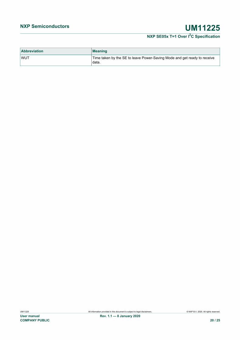
Abbreviation Meaning
WUT Time taken by the SE to leave Power-Saving Mode and get ready to receivedata.
NXP Semiconductors UM11225NXP SE05x T=1 Over I2C Specification
UM11225 All information provided in this document is subject to legal disclaimers. © NXP B.V. 2020. All rights reserved.
User manual Rev. 1.1 — 8 January 2020COMPANY PUBLIC 21 / 25
5 References
[1] ISO/IEC 7816-3:2006 Identification cards – Integrated circuit cards – Part 3: Cardswith contacts – Electrical interface and transmission protocols
NXP Semiconductors UM11225NXP SE05x T=1 Over I2C Specification
UM11225 All information provided in this document is subject to legal disclaimers. © NXP B.V. 2020. All rights reserved.
User manual Rev. 1.1 — 8 January 2020COMPANY PUBLIC 22 / 25
6 Legal information
6.1 DefinitionsDraft — The document is a draft version only. The content is still underinternal review and subject to formal approval, which may result inmodifications or additions. NXP Semiconductors does not give anyrepresentations or warranties as to the accuracy or completeness ofinformation included herein and shall have no liability for the consequencesof use of such information.
6.2 DisclaimersLimited warranty and liability — Information in this document is believedto be accurate and reliable. However, NXP Semiconductors does notgive any representations or warranties, expressed or implied, as to theaccuracy or completeness of such information and shall have no liabilityfor the consequences of use of such information. NXP Semiconductorstakes no responsibility for the content in this document if provided by aninformation source outside of NXP Semiconductors. In no event shall NXPSemiconductors be liable for any indirect, incidental, punitive, special orconsequential damages (including - without limitation - lost profits, lostsavings, business interruption, costs related to the removal or replacementof any products or rework charges) whether or not such damages are basedon tort (including negligence), warranty, breach of contract or any otherlegal theory. Notwithstanding any damages that customer might incur forany reason whatsoever, NXP Semiconductors’ aggregate and cumulativeliability towards customer for the products described herein shall be limitedin accordance with the Terms and conditions of commercial sale of NXPSemiconductors.
Right to make changes — NXP Semiconductors reserves the right tomake changes to information published in this document, including withoutlimitation specifications and product descriptions, at any time and withoutnotice. This document supersedes and replaces all information supplied priorto the publication hereof.
Suitability for use — NXP Semiconductors products are not designed,authorized or warranted to be suitable for use in life support, life-critical orsafety-critical systems or equipment, nor in applications where failure ormalfunction of an NXP Semiconductors product can reasonably be expectedto result in personal injury, death or severe property or environmentaldamage. NXP Semiconductors and its suppliers accept no liability forinclusion and/or use of NXP Semiconductors products in such equipment orapplications and therefore such inclusion and/or use is at the customer’s ownrisk.
Applications — Applications that are described herein for any of theseproducts are for illustrative purposes only. NXP Semiconductors makesno representation or warranty that such applications will be suitablefor the specified use without further testing or modification. Customersare responsible for the design and operation of their applications and
products using NXP Semiconductors products, and NXP Semiconductorsaccepts no liability for any assistance with applications or customer productdesign. It is customer’s sole responsibility to determine whether the NXPSemiconductors product is suitable and fit for the customer’s applicationsand products planned, as well as for the planned application and use ofcustomer’s third party customer(s). Customers should provide appropriatedesign and operating safeguards to minimize the risks associated withtheir applications and products. NXP Semiconductors does not accept anyliability related to any default, damage, costs or problem which is basedon any weakness or default in the customer’s applications or products, orthe application or use by customer’s third party customer(s). Customer isresponsible for doing all necessary testing for the customer’s applicationsand products using NXP Semiconductors products in order to avoid adefault of the applications and the products or of the application or use bycustomer’s third party customer(s). NXP does not accept any liability in thisrespect.
Limiting values — Stress above one or more limiting values (as defined inthe Absolute Maximum Ratings System of IEC 60134) will cause permanentdamage to the device. Limiting values are stress ratings only and (proper)operation of the device at these or any other conditions above thosegiven in the Recommended operating conditions section (if present) or theCharacteristics sections of this document is not warranted. Constant orrepeated exposure to limiting values will permanently and irreversibly affectthe quality and reliability of the device.
Terms and conditions of commercial sale — NXP Semiconductorsproducts are sold subject to the general terms and conditions of commercialsale, as published at http://www.nxp.com/profile/terms, unless otherwiseagreed in a valid written individual agreement. In case an individualagreement is concluded only the terms and conditions of the respectiveagreement shall apply. NXP Semiconductors hereby expressly objects toapplying the customer’s general terms and conditions with regard to thepurchase of NXP Semiconductors products by customer.
No offer to sell or license — Nothing in this document may be interpretedor construed as an offer to sell products that is open for acceptance orthe grant, conveyance or implication of any license under any copyrights,patents or other industrial or intellectual property rights.
Export control — This document as well as the item(s) described hereinmay be subject to export control regulations. Export might require a priorauthorization from competent authorities.
Translations — A non-English (translated) version of a document is forreference only. The English version shall prevail in case of any discrepancybetween the translated and English versions.
6.3 TrademarksNotice: All referenced brands, product names, service names andtrademarks are the property of their respective owners.
NXP Semiconductors UM11225NXP SE05x T=1 Over I2C Specification
UM11225 All information provided in this document is subject to legal disclaimers. © NXP B.V. 2020. All rights reserved.
User manual Rev. 1.1 — 8 January 2020COMPANY PUBLIC 23 / 25
TablesTab. 1. Revision history .................................................2Tab. 2. T=1 Frame Format ............................................4Tab. 3. 3-Byte Prologue ................................................ 4Tab. 4. NAD Format ...................................................... 4Tab. 5. SAD/DAD values ...............................................4Tab. 6. Coding of I-Block PCB ...................................... 5Tab. 7. Coding of R-Block PCB .....................................5Tab. 8. R-Block Error codes ..........................................5Tab. 9. Generic S-Block Coding ....................................6
Tab. 10. Coding of S-Block PCB .....................................6Tab. 11. Block Types .......................................................7Tab. 12. ATR – Common Structure .................................8Tab. 13. ATR – Specific Parameters for Data Link
Layer ................................................................. 8Tab. 14. ATR – Specific Parameters for I2C Physical
Layer ................................................................. 9Tab. 15. I2C Default Values .......................................... 18Tab. 16. Abbreviations ...................................................19
NXP Semiconductors UM11225NXP SE05x T=1 Over I2C Specification
UM11225 All information provided in this document is subject to legal disclaimers. © NXP B.V. 2020. All rights reserved.
User manual Rev. 1.1 — 8 January 2020COMPANY PUBLIC 24 / 25
FiguresFig. 1. T=1 over I2C Communication Stack ................. 3Fig. 2. SE I2C Slave State Machine ...........................11Fig. 3. Simplified I2C Schematics .............................. 12Fig. 4. I2C Frame - HD to SE .................................... 12Fig. 5. HD Sends Data to SE .....................................13Fig. 6. HD Polling SE for Response Data .................. 14
Fig. 7. I2C frame - SE to HD ..................................... 15Fig. 8. I2C multiple frames - SE to HD .......................15Fig. 9. SE sends data to HD ...................................... 15Fig. 10. I2C multiple frames - SE to HD .......................16Fig. 11. HD Read Sequence ........................................ 17
NXP Semiconductors UM11225NXP SE05x T=1 Over I2C Specification
Please be aware that important notices concerning this document and the product(s)described herein, have been included in section 'Legal information'.
© NXP B.V. 2020. All rights reserved.For more information, please visit: http://www.nxp.comFor sales office addresses, please send an email to: [email protected]
Date of release: 8 January 2020
Contents1 Introduction ......................................................... 22 Data Link Layer (T=1) ......................................... 32.1 T=1 Block Frame Format .................................. 42.1.1 Prologue Field ................................................... 42.1.1.1 Node Address Byte (NAD) ................................ 42.1.1.2 Protocol Control Byte (PCB) ..............................42.1.1.3 Information Field Length (LEN) ......................... 72.1.2 Information Field (INF) .......................................72.1.2.1 Information Field Size (IFS) ...............................72.1.3 Epilogue Field (CRC) ........................................ 82.2 Answer to Reset (ATR) ..................................... 82.2.1 ATR – Common Structure ................................. 82.2.2 ATR – Specific Parameters for Data Link
Layer ..................................................................82.2.3 ATR – Specific Parameters for I2C Physical
Layer ..................................................................92.3 Rules for Error-Free Operation ..........................92.3.1 Initialization ........................................................ 92.3.2 Processing ......................................................... 92.3.3 Acknowledgement ..............................................92.3.4 Waiting Time Extension ...................................102.4 Error handling .................................................. 102.4.1 Re-transmission ............................................... 102.4.2 Error Recovery ................................................ 103 Physical Interfaces ............................................113.1 I2C Interface .................................................... 113.1.1 Description ....................................................... 113.1.1.1 SE I2C Receive State ..................................... 123.1.1.2 SE I2C Processing State .................................133.1.1.3 SE I2C Send State .......................................... 143.1.1.4 SE I2C Default Values .....................................174 Abbreviations and Notations ........................... 195 References ......................................................... 216 Legal information ..............................................22