Embed Size (px)
Citation preview
ORNL/TM-2009/236
Energy and Transportation Science Division
Oak Ridge National Laboratory Annual Progress Report for the Power
Electronics and Electric Machinery Program
Mitch Olszewski, Program Manager
October 2009
Prepared by OAK RIDGE NATIONAL LABORATORY
Oak Ridge, Tennessee 37831 managed by
UT-BATTELLE, LLC for the
U.S. DEPARTMENT OF ENERGY under contract DE-AC05-00OR22725

DOCUMENT AVAILABILITY Reports produced after January 1, 1996, are generally available free via the U.S. Department of Energy (DOE) Information Bridge. Web site http://www.osti.gov/bridge Reports produced before January 1, 1996, may be purchased by members of the public from the following source. National Technical Information Service 5285 Port Royal Road Springfield, VA 22161 Telephone 703-605-6000 (1-800-553-6847) TDD 703-487-4639 Fax 703-605-6900 E-mail [email protected] Web site http://www.ntis.gov/support/ordernowabout.htm Reports are available to DOE employees, DOE contractors, Energy Technology Data Exchange (ETDE) representatives, and International Nuclear Information System (INIS) representatives from the following source. Office of Scientific and Technical Information P.O. Box 62 Oak Ridge, TN 37831 Telephone 865-576-8401 Fax 865-576-5728 E-mail [email protected] Web site http://www.osti.gov/contact.html
This report was prepared as an account of work sponsored by an agency of the United States Government. Neither the United States Government nor any agency thereof, nor any of their employees, makes any warranty, express or implied, or assumes any legal liability or responsibility for the accuracy, completeness, or usefulness of any information, apparatus, product, or process disclosed, or represents that its use would not infringe privately owned rights. Reference herein to any specific commercial product, process, or service by trade name, trademark, manufacturer, or otherwise, does not necessarily constitute or imply its endorsement, recommendation, or favoring by the United States Government or any agency thereof. The views and opinions of authors expressed herein do not necessarily state or reflect those of the United States Government or any agency thereof.
U.S. Department of Energy FreedomCAR and Vehicle Technologies, EE-2G
1000 Independence Avenue, S.W. Washington, D.C. 20585-0121
FY 2009 Oak Ridge National Laboratory Annual Progress Report for the Power Electronics and Electric Machinery Program Prepared by: Oak Ridge National Laboratory Mitch Olszewski, Program Manager Submitted to: Energy Efficiency and Renewable Energy Vehicle Technologies Program Susan A. Rogers, Technology Development Manager October 2009
Power Electronics and Electric Machines FY 2009 Progress Report
iii
Contents
Page
Acronyms and Abbreviations ................................................................................................................ v
1. Introduction ..................................................................................................................................... 1
2. Thermal Management Systems ....................................................................................................... 5
2.1 Direct Cooled Power Electronics Substrate .......................................................................... 5
3. Electric Machinery Research and Technology Development ......................................................... 17
3.1 A New Class of Switched Reluctance Motors ...................................................................... 17
3.2 Novel Flux Coupling Machine without Permanent Magnets ................................................ 27
4. Power Electronics Research and Technology Development ........................................................... 37
4.1 Wide Bandgap Materials ....................................................................................................... 37
4.2 An Active Filter Approach to the Reduction of the DC Link Capacitor ............................... 48
4.3 High Temperature, High Voltage Fully Integrated Gate Driver Circuit ............................... 57
4.4 Current Source Inverter ......................................................................................................... 70
4.5 Using the Traction Drive Power Electronics System to Provide Plug-In Capability for Hybrid Electric Vehicles ................................................................................ 82
4.6 A Segmented Drive System with a Small DC Bus Capacitor ............................................... 95
5. Systems Research and Technology Development ........................................................................... 103
5.1 Benchmarking of Competitive Technologies ........................................................................ 103

Power Electronics and Electric Machines FY 2009 Progress Report
v
Acronyms and Abbreviations
3D three-dimensional
3G third generation
Al2O3 aluminum oxide or alumina
ac alternating current
Alnico aluminum-nickel-cobalt (alloy used to make permanent magnets)
APEEM Advanced Power Electronics and Electric Machines
APF active power filter
BGR bandgap voltage reference
CMOS complementary metal-oxide semiconductor
CSI current source inverter
DBC direct bonded copper
dc direct current
DMOS double diffused metal-oxide semiconductor
DOE U.S. Department of Energy
DSP digital signal processing
ECVT electronically controlled continuously variable transmission
EDS energy dispersive x-ray spectroscopy
EETT Electrical and Electronics Technical Team
EMF electromotive force
EMI electromagnetic interference
EOL end-of-life
ETA Electric Transportation Applications
EV electric vehicle
FEA finite element analysis
fm modulation frequency (inverter)
fsw switching frequency (inverter)
HEV hybrid electric vehicle
HSF hard switch fault
HVNMOS high voltage NMOS
ID inner diameter
IGBT insulated gate bipolar transistor
IM induction motor
IMFP isolated multiple flux path
INL Idaho National Laboratory
INV/CONV inverter/converter
IPM internal permanent magnet
JBS junction barrier Schottky (device/diode)

FY 2009 Progress Report Power Electronics and Electric Machines
vi
JFET junction field-effect transistor
Ld direct axis inductance (IPM motor)
Lq quadrature axis inductance (IPM motor)
LCR inductance, capacitance, resistance (as in an LCR meter, used to measure impedance)
MG motor/generator
MOSFET metal-oxide semiconductor field-effect transistor
NMOS n-channel metal-oxide semiconductor
OD outer diameter
ORNL Oak Ridge National Laboratory
OTA operational transconductance amplifier
PCU power control unit
PE power electronic
pF power factor
PHEV plug-in hybrid electric vehicle
PI proportional-integral
PM permanent magnet
PMOS p-channel metal-oxide semiconductor
p-p peak-to-peak
PSIM Powersim (circuit simulation software)
PWM pulse-width modulation
R24 conceptual design revision 24 (for the Novel Flux Coupling Machine without PMs)
RMS root mean square
SiC silicon carbide
SPICE Simulation Program with Integrated Circuit Emphasis
SOI silicon-on-insulator
SR switched reluctance
SRM switched reluctance motor
UVLO undervoltage lockout
Vdc dc voltage
Vgs gate-source voltage
VSATT Vehicle Systems Analysis Technical Team
VSI voltage source inverter
WBG wide bandgap
WEG water-ethylene glycol
ZTC zero-temperature coefficient

Power Electronics and Electric Machines FY 2009 Progress Report
1
1. Introduction
The U.S. Department of Energy (DOE) and the U.S. Council for Automotive Research (composed of automakers Ford, General Motors, and Chrysler) announced in January 2002 a new cooperative research effort. Known as FreedomCAR (derived from “Freedom” and “Cooperative Automotive Research”), it represents DOE’s commitment to developing public/private partnerships to fund high-risk, high-payoff research into advanced automotive technologies. Efficient fuel cell technology, which uses hydrogen to power automobiles without air pollution, is a very promising pathway to achieve the ultimate vision. The new partnership replaces and builds upon the Partnership for a New Generation of Vehicles initiative that ran from 1993 through 2001. The Oak Ridge National Laboratory’s (ORNL’s) Advanced Power Electronics and Electric Machines (APEEM) subprogram within the Vehicle Technologies Program provides support and guidance for many cutting-edge automotive technologies now under development. Research is focused on understanding and improving the way the various new components of tomorrow’s automobiles will function as a unified system to improve fuel efficiency. In supporting the development of advanced vehicle propulsion systems, the APEEM effort has enabled the development of technologies that will significantly improve efficiency, costs, and fuel economy. The APEEM subprogram supports the efforts of the FreedomCAR and Fuel Partnership through a three-phase approach intended to • identify overall propulsion and vehicle-related needs by analyzing programmatic goals and reviewing
industry’s recommendations and requirements and then develop the appropriate technical targets for systems, subsystems, and component research and development activities;
• develop and validate individual subsystems and components, including electric motors and power electronics; and
• determine how well the components and subsystems work together in a vehicle environment or as a complete propulsion system and whether the efficiency and performance targets at the vehicle level have been achieved.
The research performed under this subprogram will help remove technical and cost barriers to enable the development of technology for use in such advanced vehicles as hybrid electric vehicles (HEVs), plug-in HEVs (PHEVs), all electric vehicles, and fuel-cell–powered automobiles that meet the goals of the Vehicle Technologies Program. A key element in making these advanced vehicles practical is providing an affordable electric traction drive system. This will require attaining weight, volume, and cost targets for the power electronics and electrical machines subsystems of the traction drive system. Areas of development include these: • novel traction motor designs that result in increased power density and lower cost; • inverter technologies involving new topologies to achieve higher efficiency, with the ability to
accommodate higher-temperature environments while achieving high reliability; • converter concepts that employ means of reducing the component count and integrating functionality
to decrease size, weight, and cost; • new onboard battery charging concepts that result in decreased cost and size; • more effective thermal control and packaging technologies; and • integrated motor/inverter concepts.

FY 2009 Progress Report Power Electronics and Electric Machines
2
ORNL’s Power Electronics and Electric Machinery Research Center conducts fundamental research, evaluates hardware, and assists in the technical direction of the DOE Vehicle Technologies Program, APEEM subprogram. In this role, ORNL serves on the FreedomCAR Electrical and Electronics Technical Team, evaluates proposals for DOE, and lends its technological expertise to the direction of projects and evaluation of developing technologies. ORNL also executes specific projects for DOE. The following report discusses those projects carried out in FY 2009 and conveys highlights of their accomplishments. Numerous project reviews, technical reports, and papers have been published for these efforts, if the reader is interested in pursuing details of the work. Below are summaries of major accomplishments for each technical project. Direct Water-Cooled Power Electronics Substrate
• Simulated various designs using thermal and mechanical finite element analysis. • Fabricated direct bonded copper substrates (copper clad, plated, and dies attached with ribbon bonds). • Fabricated a test fixture and completed flow tests on prototypes utilizing water–ethylene glycol at
various temperatures, including 105°C. • Validated models based on comparisons between experimental results and modeling results. A New Class of Switched Reluctance Motors
• Assessed feasibility of various design techniques and selected a preferred methodology. • Developed and simulated hardware and software solutions for reducing torque ripple and acoustic
noise. — Demonstrated that for low and moderate torque levels, near zero torque ripple could be achieved.
• Demonstrated the potential for increased power density via continuous conduction control. • Developed two universal dynamic simulators (crucial for structural and acoustic noise modeling).
— Parametric simulator: efficient means to optimize control and design parameters. — Finite element analysis simulator: highly accurate, but more suited for known control and design
conditions. Novel Flux Coupling Machine without Permanent Magnets
• Completed the development of analytical tools used for the design of the novel flux coupling machine without permanent magnets.
• Performed electromagnetic simulations for motor performance and mechanical finite element analysis for rotational stress loading for design optimization.
Wide Bandgap Materials
• Acquired, tested, and characterized silicon carbide (SiC) junction field-effect transistors (JFETs), metal-oxide semiconductor field-effect transistors (MOSFETs), and diodes.
• Completed evaluation of a 10 kW SiC JFET-based inverter. • Completed the feasibility study of an air-cooled 55 kW inverter design. An Active Filter Approach to the Reduction of the dc Link Capacitor
• Built a simulation model of a traction drive system to establish the performance requirements for an active power filter (APF).

Power Electronics and Electric Machines FY 2009 Progress Report
3
• Analyzed the parameter dependence of the APF and the underlying barriers of this method. • Demonstrated the tradeoff in losses against the reduction in dc bus capacitance through the use of an
APF. High Temperature, High Voltage Fully Integrated Gate Driver Circuit
• Designed and taped out the third generation (3G) gate driver circuit, which has current drive strength of more than 5 A at room temperature.
• Optimized design by making some of the critical functional blocks in the 3G gate driver circuit temperature insensitive.
• Incorporated multiple voltage regulator circuits in the gate driver chip. • Integrated short-circuit protection, undervoltage lockout, and thermal shutdown circuitries with the
core gate driver circuit. Current Source Inverter for HEVs and Fuel Cell Vehicles
• Derived analytical equations for computing the average losses of insulated gate bipolar transistors (IGBTs) and diodes in the current source inverter (CSI) topology.
• Completed a custom IGBT module design for the CSI switch leg using Infineon IGBT and Semikron diode chips rated with maximum junction temperature of 175°C.
• Completed a design for a 55 kW CSI for operation with a 105°C coolant using the custom IGBT modules. The total capacitance is 390 μF. Estimated IGBT and diode junction temperatures are 148.2 and 134.1°C, respectively, which are well within their safe operating region.
• Designed and fabricated digital signal processors and gate drive boards for operation in the 105°C coolant environment using components rated in the automotive temperate range of -40 to ~125°C.
Using the Traction Drive Power Electronics System to Provide Plug-in Capability for PHEVs
• Designed, fabricated, and successfully tested an HEV power electronics system prototype consisting of a 55 kW motor inverter and a 30 kW generator inverter for operation as a battery charger and mobile power generator. — Attained a maximum charging efficiency greater than 95% with a 120 V input and greater than
98% with a 240 V input. — Attained a grid current harmonic distortion factor of less than 9% at 120 V input and less than 7%
at 240 V input at rated power during charging operation. — Attained a maximum efficiency of 80% with a 120 V output in engine-powered generation mode. — Attained a maximum efficiency of 97% at 240 V output and 94% at 120 V output in battery-
powered generation mode. A Segmented Drive System with a Small dc Bus Capacitor
• Validated the segmented drive concept through a simulation study. — Achieved more than 65% reduction in capacitor ripple current compared with the standard
inverter configuration. — Achieved 80% reduction in battery ripple current. — Achieved 70% reduction in dc bus ripple voltage. — Achieved 50% reduction in motor ripple current. — Completed a conceptual design for a 55 kW prototype.

FY 2009 Progress Report Power Electronics and Electric Machines
4
Benchmarking of Competitive Technologies
• Conducted end-of-life (EOL) assessments to find and explore any detrimental impacts sustained over the life of a 2004 Toyota Prius.
• Compared observations from EOL assessments to those made during original benchmarking of the 2004 Prius.
• Determined that subcomponents of the 2004 Toyota Prius sustained no substantially negative impacts.
• Conducted preliminary design/packaging studies of the 2010 Prius power control unit and electrically controlled variable transmission, wherein significant differences with respect to the 2004 Toyota Prius were noted.
Power Electronics and Electric Machines FY 2009 Progress Report
5
2. Thermal Management Systems
2.1 Direct Cooled Power Electronics Substrate
Principal Investigator: Randy H. Wiles Oak Ridge National Laboratory National Transportation Research Center 2360 Cherahala Boulevard Knoxville, TN 37932 Voice: 865-946-1319; Fax: 865-946-1262; E-mail: [email protected] DOE Technology Development Manager: Susan A. Rogers Voice: 202-586-8997; Fax: 202-586-1600; E-mail: [email protected] ORNL Program Manager: Mitch Olszewski Voice: 865-946-1350; Fax: 865-946-1262; E-mail: [email protected] Objectives The FY 2009 project objective was to finalize the design requirements for the selected architecture for a direct cooled power electronics substrate which will result in reductions in size and volume of the inverter power electronics, achieving the 2015 DOE FreedomCAR target of at least 12.0 kW/L while operating with an elevated coolant temperature of 105°C. Proposed Solution To use 105°C coolant for heat dissipation from the electronics, the coolant paths must be placed as close to the chip junction as possible. This project explores a direct cooled power electronics substrate which incorporates cooling channels directly in the ceramic of a direct bonded copper (DBC) substrate. The overall structure of the direct cooled substrate is a hexagonal and/or an octagonal prism. This shape simplifies the fluid seals and provides a unique structure for die attachment. The approach presented also highlights the benefits of designing the power electronics package and inverter package in parallel. Approach • Finalize the design requirements for a single leg prototype power electronics mounting structure DBC
substrate. • Perform a final thermal simulation as well as a mechanical stress simulation on the selected design
structures and use the finite element analysis (FEA) results as a basis for comparison of FY 2009 test results.
• Complete the assembly of the single leg prototype direct cooled DBC designs as follows. — Manufacture the selected ceramic substrate designs. — Design, purchase components, and fabricate the testing apparatus. — Finalize the substrate fabrication (copper cladding and plating). — Assemble components onto the substrate (diode attachment and wire/ribbon bonds).
• Test the assembled prototypes. — Instrument and install assembled prototypes in the testing apparatus. — Test assembled prototypes using 105°C water-ethylene glycol (WEG) coolant.

FY 2009 Progress Report Power Electronics and Electric Machines
6
Major Accomplishments • Designs were selected. • Thermal and mechanical FEA results were obtained. • DBC substrates were fabricated (copper clad, plated, and dies attached with ribbon bonds applied). • Flow tests were completed. • FEA models were updated and comparisons made based on experimental flow results. • Prototypes were assembled, instrumented, and tested using various WEG temperatures, including
105°C. • Model validations were performed based on comparisons between experimental results and modeling
results. Future Direction • Iterate mechanical design based on FY 2009 laboratory test results. • Fabricate and assemble the next generation inverter prototype. • Finalize inverter prototype design and testing. Technical Discussion The goal of the Direct Cooled Power Electronics Substrate project is to enable the use of 105°C coolant with the power electronic components used in hybrid electric and plug-in hybrid electric vehicles (HEVs and PHEVs). The proposed concept in this project was to develop an innovative power electronics mounting structure, generate three-dimensional models, and perform both thermal and mechanical FEA. This concept involved integrating cooling channels within the DBC substrate and strategically locating these channels underneath the power electronic devices. Reducing the size and weight of the heat sink for power electronics are among the other benefits sought. Of the design concepts modeled, two of the most promising designs were fabricated, assembled, and tested. These designs took into account issues such as containment of the fluid (separation from the electronics) and synergy with the whole power inverter design architecture. Testing results were compared to the final FEA modeling performed on the two designs to validate both the modeling results and the success of the design approach. Information contained in this annual report serves as a general discussion of this research effort. For more detailed information, please refer to Preliminary Testing Results of Direct Cooled Power Electronics Substrate, ORNL/TM-2009/204 [1]. Recap of FY 2008 Work In FY 2008, the research effort showed that a ceramic heat exchanger concept involving 105°C WEG cooling was a viable option. Several design iterations including FEA results for each design were performed. A performance matrix and weighting system was developed to help evaluate the effectiveness of each design. These design matrix summaries are listed in Direct Cooled Power Electronics Substrate, ORNL/TM-2008/112, Tables 7–13 [2]. They contain the loads, thermal data resulting from the use of three or four insulated gate bipolar transistors (IGBTs), manufacturing variables and trade-offs, and cost to manufacture in quantities of 100,000 pieces. Based on cost evaluations, research was geared primarily toward alumina (Al2O3) as the substrate material. The overall size of the structure grew to accommodate more heat spreading, which is required because of Al2O3’s lower thermal conductivity compared with other candidate ceramic materials. Knowing that Al2O3 was inert to WEG, compatibility tests were completed to demonstrate the effect of

Power Electronics and Electric Machines FY 2009 Progress Report
7
50/50 WEG on other candidate ceramics. The annular substrate and the four-hole substrate were two of the most promising design iterations. These were selected for the second phase of the research effort. Selection of Final Single Leg Prototype Designs Detailed models of the annular substrate and the four-hole substrate were run. These models include more geometry detail such as rounded ends, wire bonds, actual chip sizes, and distributed loading. The original models from FY 2008 had a copper cladding thickness of 0.050 in. (1.27 mm). The first quote from a vendor was to clad the substrate with 0.020 in. (0.5 mm) copper. After some debate, a few models were run to compare cladding thickness differences. The thinner cladding increases the junction temperature of the chip by 5ºC. Thus the copper cladding should be as thick as possible. One vendor was able to provide a quote for 0.050 in. thick cladding; therefore this thickness was used for the thermal models. Because the flow properties of the thermal enhancing metal matrix were unknown at this time, three separate approaches to model the porous media flows were run for each design case to establish an operational range. The Darcy model, which assumed a plug flow or flat velocity profile, was used in FY 2008. The Darcy flow model resulted in the lowest temperature predictions because of the large velocity gradient at the wall. The parameters used for the porous media model were taken from the literature for comparable applications [3]. The permeability for aluminum foams with similar specifications is on the order of 1e-8 m2. This permeability provides a high flow restriction that increases the difficulty of obtaining a converged solution. For a basic comparison and simpler computational scheme the permeability was 1e-4 m2, and the porosity was 0.89. The Darcy model forms the lower bound of the operational range. The Brinkman porous media flow model takes into account the viscous effects at the inner wall of the flow channel, which results in a more parabolic velocity profile. The decrease in velocity gradient at the channel wall results in less heat transfer to the fluid. This model is only valid for laminar flows. The flow parameters were consistent with the Darcy model. In general, the Brinkman model produces the highest junction and fluid temperatures. It forms the upper bound of the operational range. However, the Brinkman model does not account for the turbulent mixing within the metal foam inserted in the flow channels. A Brinkman model with a Forchheimer correction flattens the velocity profile. The flatter profile increases the velocity gradient near the wall, which causes more local heat transfer. This effect lowers the maximum temperatures compared with the Brinkman model but not to the point of equaling the Darcy model. The Brinkman model with the Forchheimer correction is believed to be more accurate because it accounts for the added flow resistance resulting from turbulence. The Forchheimer friction coefficient was calculated from a correlation in the literature [4]. Annular Design The results for the three cases are shown in Table 1. The highest predicted temperature is above the desired 150°C but still below the absolute maximum of 175°C. As predicted, the Darcy model forms the lower bound, and the Brinkman model forms the upper bound. All diode temperatures are below the 150°C design point. The Brinkman model also shows the fluid wall temperature exceeding the boiling point of the 50/50 WEG, but the other two models are below the 130°C limit. These results show that the operational range of the direct cooled annular substrate is reasonable with respect to the design parameters and the material property assumptions.

FY 2009 Progress Report Power Electronics and Electric Machines
8
Table 1. Thermal Modeling Results for Annular Design
Maximum temperatures
Darcy Brinkman Brinkman with Forchheimer
correction
TIGBT (ºC) 149.9 156.6 154.8 Tdiode (ºC) 143.5 149.7 148.1 Tfluid (ºC) 123.1 131 128.8
Four-Hole Design The results of the three flow cases for the four-hole design are shown in Table 2. The Darcy model resulted in a maximum fluid wall temperature close to the maximum allowable temperature. Modeling the Brinkman and Forchheimer correction confirmed the fluid temperature would exceed the boiling point. The other flow models result in increases in the predicted junction temperatures. The chips can theoretically survive at these temperatures, but their reliability may be compromised. Because the nonconservative models predict temperatures above boiling, the actual junction temperatures may be lower because of phase change effects. On the other hand they may be higher because of local hot spots and bubble formation. The model does not account for the latent energy exchange at boiling and thus cannot accurately prescribe junction temperatures if the boiling point is exceeded. The operational range for the four-hole design extends beyond the design limits but may be improved with further work on hole size and placement.
Table 2. Thermal Modeling Results for Four-Hole Design
Maximum temperatures
Darcy Brinkman Brinkman with Forchheimer
correction
TIGBT (ºC) 150.8 160.0 156.0 Tdiode (ºC) 152.9 160.4 156.9 Tfluid (ºC) 127.7 139.7 134.3
From the modeling with all properties determined by engineering estimates, the annular structure should perform better than the four-hole design. Flow properties and thermal validation experimentation were used to evaluate the accuracy of the model parameters. Mechanical FEA Results The two designs were also evaluated through a statistical mechanics program intended to determine the probability of failure for ceramic components. The four-hole design had a probability of failure of 4 ppm. The annular design had a probability of failure of 8 ppm. These evaluations were based on the thermal fatigue from the temperature distribution found at the end of FY 2008. The survivability of both parts is well within an acceptable range. Experimental Flow Test Results In previous modeling, the aluminum foam was modeled using several governing equations for porous media. This modeling was used to provide a range of temperatures for the ceramic substrate and electronics because the exact properties of the foam were unknown at the time. Upon receipt of the aluminum foam, the porosity was measured. The annular pieces had an average porosity of 0.90, and the cylinders for the four-hole design had an average porosity of 0.91. These values reflect a maximum of a 2% increase over the assumed value of 0.89 in previous modeling.
Power Electronics and Electric Machines FY 2009 Progress Report
9
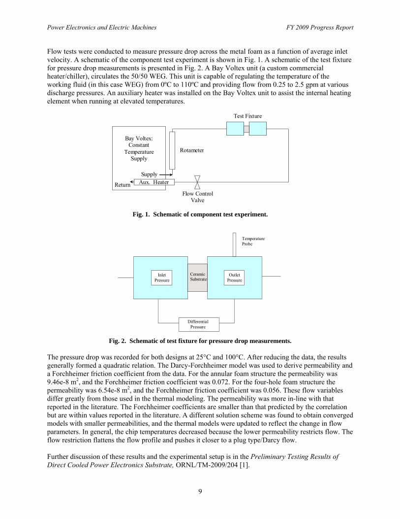
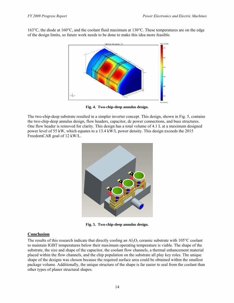
Flow tests were conducted to measure pressure drop across the metal foam as a function of average inlet velocity. A schematic of the component test experiment is shown in Fig. 1. A schematic of the test fixture for pressure drop measurements is presented in Fig. 2. A Bay Voltex unit (a custom commercial heater/chiller), circulates the 50/50 WEG. This unit is capable of regulating the temperature of the working fluid (in this case WEG) from 0ºC to 110ºC and providing flow from 0.25 to 2.5 gpm at various discharge pressures. An auxiliary heater was installed on the Bay Voltex unit to assist the internal heating element when running at elevated temperatures.
Supply
Return
Bay Voltex: Constant
Temperature Supply
Rotameter
Aux. Heater
Flow Control Valve
Test Fixture
Fig. 1. Schematic of component test experiment.
Temperature Probe
Inlet Pressure
Outlet Pressure
Differential Pressure
Ceramic Substrate
Fig. 2. Schematic of test fixture for pressure drop measurements.
The pressure drop was recorded for both designs at 25°C and 100°C. After reducing the data, the results generally formed a quadratic relation. The Darcy-Forchheimer model was used to derive permeability and a Forchheimer friction coefficient from the data. For the annular foam structure the permeability was 9.46e-8 m2, and the Forchheimer friction coefficient was 0.072. For the four-hole foam structure the permeability was 6.54e-8 m2, and the Forchheimer friction coefficient was 0.056. These flow variables differ greatly from those used in the thermal modeling. The permeability was more in-line with that reported in the literature. The Forchheimer coefficients are smaller than that predicted by the correlation but are within values reported in the literature. A different solution scheme was found to obtain converged models with smaller permeabilities, and the thermal models were updated to reflect the change in flow parameters. In general, the chip temperatures decreased because the lower permeability restricts flow. The flow restriction flattens the flow profile and pushes it closer to a plug type/Darcy flow. Further discussion of these results and the experimental setup is in the Preliminary Testing Results of Direct Cooled Power Electronics Substrate, ORNL/TM-2009/204 [1].

FY 2009 Progress Report Power Electronics and Electric Machines
10
Prototype Manufacturing and Assembly The ceramic substrate geometries fabricated by CoorsTek were received with reasonably flat surfaces and within the design specifications. The substrates were fabricated using an injection molding process to produce the “green” parts and were then fired to complete the final product. Upon inspection of the flat surfaces, the total surface flatness on the parts was within 0.001 in. to 0.002 in. The flat surfaces are necessary for the die attachment, especially if the dies are to be sintered into position. Finalize Substrate Fabrication (Copper Cladding and Plating) Once the substrates were received from CoorsTek, the next process was to have each of the flat surfaces metalized with copper. The copper has to be intimately bonded to the ceramic to promote heat transfer. Aegis Technology, Inc., of Santa Ana, California, was contracted to complete this task. Before the parts were returned, the copper was nickel-gold plated to help with the chip soldering/sintering. The gold plating and presumably the nickel plating wrapped the edges onto the sealing boss. A test was performed using a mega-ohm testing unit to determine that the two landing areas (the 12 mm wide flat for diode attachment and the 5 mm flat for wire bond attachment) were isolated from each other. Each metalized substrate passed a mega-ohm test at 1,000 V. Some flaking in the plating layer was noticed, but it seemed to be adhering in the critical locations (i.e., under the diode footprint). After metallization and plating, the next step in the fabrication process was die attachment. The substrates were sent to NBE Technologies, LLC, of Blacksburg, Virginia, to have the chips soldered in position on the 12 mm flats. Soldering was chosen as the attachment method because of time restraints and because sintering requires silver plating. NBE Technologies advised ORNL after receiving the parts that some of the gold plating was coming off with scotch tape. They were concerned about the diodes not adhering well. Once the parts were in process, NBE Technologies contacted ORNL with the information that the flats of the hexagon were extremely uneven (on the order of 0.010 in. from the center to the edge). The ceramic had a reasonably flat surface; thus the copper cladding flatness was insufficient. They also reported that they had soldered three substrates, but air gaps under portions of the diodes were visible to the naked eye. NBE Technologies advised ORNL that a surface should be flat within ~5 µm for a sintering process to be attempted. This requirement translates into a 128-microinch finish or better. Upon receiving the parts back from NBE Technologies, ORNL had a machine shop attempt to flatten the surfaces. They were also asked to remove the plating that overlapped the edges. As they began to prepare the surfaces, they noticed that the copper cladding was moving and could not be flattened well because it was expanding from the heat and stress of the machining operation. Also they were finding air gaps under the copper cladding when the overlap was removed. Later discussions with Aegis Technology would confirm that they attempted to braze this 0.050 in. thick piece onto the initial 0.020 in. metalized area and had to go through several reheats because the brazing material was not filling the large gap. ORNL removed the outer thick layer of copper and noticed a large amount of oxidation between the direct bonded copper and the outer copper cladding. The bonding method used to attach the 0.050 in. hexagonal copper components was unsuccessful. However, after close inspection of the surface, it was noted that the initial 0.010–0.020 in. metallization layer adhered well. To evaluate this problem, the DBC layer was cleaned off. The parts were returned to Aegis Technology to have another layer of DBC (0.020 in.) applied. This 0.020 in. layer is deemed sufficient to carry current around the edges of the hexagonal substrate. The flats then had thicker pads (0.050 in.) brazed directly onto them. Using discrete landings will allow for a smaller gap which the braze material should fill with

Power Electronics and Electric Machines FY 2009 Progress Report
11
ease. The parts were returned and cleaned up at a local machine shop to prepare the copper surface. The problem with brazing the thicker pads directly to the initial metallization layer was still present. The initial substrates prepared with soldered dies from NBE Technologies were sent to Orthodyne Electronics of Mineola, New York, to wire bond. Orthodyne noted that aluminum wire bonds were not adhering to the electroless gold plate very well. It is unknown whether this was due to the quality of the plating, unevenness/roughness of the plating, or a material incompatibility. Ideally, wire bonding directly onto an aluminized copper surface is best; however, wire bonds should be able to be attached to nickel-silver plating on copper or silver plating on copper. Further investigation and discussions took place to determine the best surface preparation. To avoid compromising the ceramic parts, different plating materials and techniques were explored using sample pieces of copper. Other plating options were discussed with the die-attachment vendor (NBE Technologies) and the wire bonder (Orthodyne). For die attachment, nickel or electroless nickel should be fine for soldering. Silver plating is needed for the sintering process. Orthodyne has done previous research on aluminum wire bonding compatibility with various plating materials. They suggested using nickel or aluminum plating. They also provided the technical specifications for the nickel plating process to produce the best results (2.5–4 µm in an 8–12% phosphorous bath). The performance of various electroless nickel samples from several vendors produced varying results. The samples finished using the specifications from Orthodyne produced the best results. Other batch samples sent for testing were heated to 300°C for 30 minutes before wire bonding. This process would simulate the heat cycle of the die attachment. No excessive cleaning was done between heating and wire bonding. Any surface oxidation caused by the elevated processing temperatures had little to no effect on the wire bonding process. Samples of nickel-silver, silver, and nickel plated on copper were sent to NBE Technologies for evaluation. Results showed that the nickel-silver plating worked quite well. The sintering paste stuck very well on both the nonheated and the heated parts. The sintering paste did not stick to the silver on copper plating. Samples of AlumiPlate aluminum plating were also obtained. These samples were plated with high purity aluminum on copper. These samples were sent for wire bonding and bond strength testing. Samples that were heated as received were tested, and the bonds and bond strength were very good. Wire bond pull test results were received from Orthodyne. The conclusions drawn from the Orthodyne wire bond pull test results are as follows. • AlumiPlate looks very promising in regards to wire and PowerRibbon bonding. • Further work will need to be done to optimize bond parameters to increase the amount of remnant
post-shear for both first and (especially) second bonds. All of the wire pull results were breaks and not lifts. Breaks are the preferred type as that is indicative that the bond is firmly attached to the surface. A majority of the wire breaks were mid-span, which is the best mode. From these tests, it was determined that the path forward would be to nickel-silver plate the die attachment landing, and the wire bond landings will be covered with aluminum plating by AlumiPlate.

FY 2009 Progress Report Power Electronics and Electric Machines
12
Component Assembly It had been determined previously that the post-brazing process on the surfaces for die attachment included abrasion blasting (or sand blasting) to remove the oxidation on the copper. This left the surfaces too uneven for sintering the dies into position, but NBE Technologies was able to attach the dies using solder. As discussed previously, the brazing process used to attach the 0.050 in. thick copper to the initial 0.020 in. metallization layer was unsuccessful. Testing of the assembled substrates would have resulted in poor heat transfer due to the voids between the initial metallization layer and the thick copper layer. An alternate component assembly was conceived and used to validate the FEA method. Initial FEA results showed that a 0.020 in. thick metallization layer would meet the design requirements and result in a simpler, less expensive manufacturing process. A testing procedure to validate the models was developed using a 0.020 in. thick metalized ceramic substrate. This testing procedure uses power resistors as heaters placed directly onto the 0.020 in. thick metalized surface where diodes would normally be attached. Detailed measurements of the metalized substrate and power resistors were taken and this information was used to create a more accurate FEA part geometry for model validation. Additional FEA models were built and results were obtained using the power resistor testing configuration. Because of the compromised cladding, the thermal validation tests should demonstrate accuracy between the modeling procedure and the experimentation. The test load may be reduced because of the thinner cladding, power restrictions on the resistor, and parasitic heat paths. Instrumentation, Installation, and Testing of Assembled Prototypes in Test Apparatus The four-hole design and the annulus design were populated with six 1-ohm 60W power resistors. Each power resistor was placed on the hexagonal flat area where the diodes were to be soldered/sintered in position. A small piece of garlite with the same footprint as the power resistor was placed on top of the resistor. The garlite piece has a slot cut into it so it will hold a thermocouple in intimate contact with the case of the power resistor for temperature measurements. This entire subassembly (power resistor, thermocouple, and garlite) is held down by a screw to maintain the surface contact between the power resistor and the metalized surface of the ceramic substrate. Each of the ceramic substrates has a piece of aluminum foam inserted into the flow channels to enhance the thermal conductivity of the ceramic into the WEG coolant. Another thermocouple is attached to each flat on the metalized ceramic substrate at the wire bond landing area. All of the power resistors are wired in series with each other. The annulus design was configured and populated in the same manner as the four-hole design. The annulus design also had a flow diverter placed inside the inner diameter of the aluminum foam. This served two purposes: to direct the flow through the foam to reduce pressure drop and to keep the inner diameter of the aluminum foam from becoming a coolant flow diverter. Each assembly was inserted into the test apparatus. The test apparatus contains a thermistor on the inlet side block and two thermistors on the outlet side block, 90 degrees apart. The inlet and outlet block have a pressure transducer mounted on each side to read the WEG inlet and outlet pressure. The apparatus was placed on an incline to ensure that the sight glass was full after the test section. The sight glass had remained full during pressure drop measurements because of the higher flow rates. The thermal validation testing takes place at 0.41 gpm. At this flow rate the sight glass does not stay full and thus not all the flow channel is filled with WEG. The incline ensures the substrate has WEG flowing through all channels. Test Results of Assembled Prototypes Using 105°C WEG The annulus design experiment was run to a maximum chip temperature of 150°C. The measured heat addition to the fluid was 64% of the design value. The reduced power level was due to the manufacturing complications previously discussed. The predicted temperature from the COMSOL model was within 6°C

Power Electronics and Electric Machines FY 2009 Progress Report
13
of the experimental results. These results were at a coolant temperature of 105°C. At 90°C coolant temperature the experiment was run at 82% of design load at a maximum chip temperature of 150°C. Again, this lower load was due to manufacturing complications. The manufacturing complications equated to a thinner copper layer than originally planned. At 90°C coolant temperature the COMSOL model prediction was within 12°C of the experimental results. The four-hole design results, having the same manufacturing complications, were also run at varying coolant temperature levels. The experiment was run at 79% design load with a maximum chip temperature of 150°C. The COMSOL model prediction was within 2.5°C of the experimental results with the chip location directly over a coolant channel. The COMSOL model was within 10°C of the experimental results with the chip location farther away from a coolant channel. At 90°C coolant temperature we ran at 88% design load with a maximum chip temperature of 150°C. The COMSOL model was within 5°C of the experimental results with the chip location directly over a coolant channel. The COMSOL model was within 16°C of the experimental results with the chip location farther away from a coolant channel. Note that the model comparisons are based on thermal models that use the measured flow parameters and have geometry and cladding that reflect the average measured copper thickness on each substrate. General Inverter Design The FEA results from this research produced promising substrate designs. A preliminary design for the inverter package was developed using the hexagonal substrate. The package, shown in Fig. 3, contains the single-chip-deep annulus design, flow headers, capacitor, direct current (dc) power connections, and buss structures. One flow header is removed for clarity. This design has a total volume of 4.4 L at a maximum designed power level of 55 kW, which equates to a 12.5 kW/L power density. This design meets the 2015 FreedomCAR goal of 12 kW/L.
Fig. 3. Single-chip-deep annulus design.
During the development of the design in Fig. 3, the dc and phase interconnects were discovered to be problematic. One way to improve upon this design and potentially reduce electromagnetic interference is to investigate a ceramic substrate that contains the entire phase leg instead of just one switch set. A preliminary model was run for an octagonal substrate with two chip sets and is shown in Fig. 4. The model parameters used were the updated ones found during the pressure drop testing. Also, the copper layer is only 0.020 in. thick. This design, also using 105°C WEG coolant, maintains the IGBT at
FY 2009 Progress Report Power Electronics and Electric Machines
14
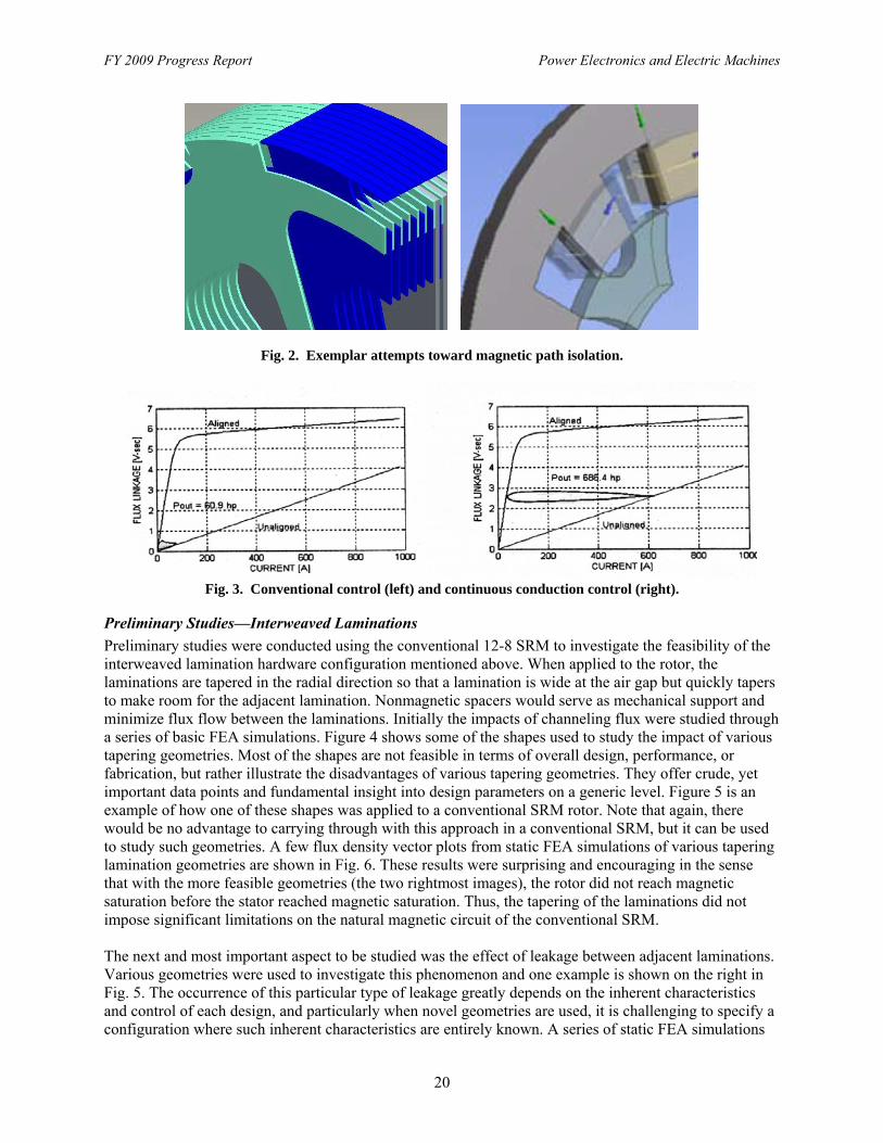
163°C, the diode at 160°C, and the coolant fluid maximum at 130°C. These temperatures are on the edge of the design limits, so future work needs to be done to make this idea more feasible.
Fig. 4. Two-chip-deep annulus design.
The two-chip-deep substrate resulted in a simpler inverter concept. This design, shown in Fig. 5, contains the two-chip-deep annulus design, flow headers, capacitor, dc power connections, and buss structures. One flow header is removed for clarity. This design has a total volume of 4.1 L at a maximum designed power level of 55 kW, which equates to a 13.4 kW/L power density. This design exceeds the 2015 FreedomCAR goal of 12 kW/L.
Fig. 5. Two-chip-deep annulus design. Conclusion The results of this research indicate that directly cooling an Al2O3 ceramic substrate with 105°C coolant to maintain IGBT temperatures below their maximum operating temperature is viable. The shape of the substrate, the size and shape of the capacitor, the coolant flow channels, a thermal enhancement material placed within the flow channels, and the chip population on the substrate all play key roles. The unique shape of the designs was chosen because the required surface area could be obtained within the smallest package volume. Additionally, the unique structure of the shape is far easier to seal from the coolant than other types of planer structural shapes.

Power Electronics and Electric Machines FY 2009 Progress Report
15
The addition of a thermal enhancement material to the flow channels provided a greater surface area within the flow channels and a better profile to remove the waste heat more efficiently. This thermal enhancement material has a much higher structural integrity compared with other types of microstructures and provided a simple means of manufacture that also met the “greater than 1mm” orifice requirement imposed by car manufacturers to protect against loose particles causing blockages. The capacitors necessary to complete the inverter design consume the majority of the total volume of the direct cooled power electronics inverter. Because this component has a larger volume than many of the other required components, volume reduction is limited by its size. With the lower cost Al2O3 substrate, the power density approaches 12.5 kW/L when the modules are packaged with a brick type capacitor. The use of hollow cylindrical capacitors did not yield any benefit to this particular design. Performance testing of the preferred designs was performed to validate the FEA results. Although there were manufacturing issues with the design, the prototype that was built still provided the necessary architecture to validate the FEA model. Publications 1. R. H. Wiles, C. W. Ayers, A.W. Wereszczak, K.T. Lowe, Preliminary Testing Results for the Direct
Cooled Power Electronics Substrate, ORNL/TM-2009/204, Oak Ridge National Laboratory, 2009.
2. Kirk T. Lowe and Rao V. Arimilli, Application of Solution Mapping to Reduce Computational Time for Actively Cooled Power Electronics, 4th Annual COMSOL conference, 2008.
References 1. R. H. Wiles, et al., Preliminary Testing Results for the Direct Cooled Power Electronics Substrate,
ORNL/TM-2009/204, Oak Ridge National Laboratory, 2009.
2. R. H. Wiles, et al., Direct Cooled Power Electronics Substrate, ORNL/TM-2008/112, Oak Ridge National Laboratory, 2008, Tables 7–13.
3. J.-P. Bonnet, F. Topin, and L. Tadrist, “Flow Laws in Metal Foams: Compressibility and Pore Size Effects,” Transport in Porous Media, Vol. 73, 2008, pp. 233–254.
4. A. Amiri and K. Vafai, “Transient analysis of incompressible flow through a packed bed,” International Journal of Heat and Mass Transfer, Vol. 41(24), 1998, pp. 4259–4279.
Patents R. H. Wiles, et al., “Direct Cooled Power Electronics Substrate,” US 2009/0231812 A1, September 17, 2009.

Power Electronics and Electric Machines FY 2009 Progress Report
17
3. Electric Machinery Research and Technology Development
3.1 A New Class of Switched Reluctance Motors
Principal Investigator: Tim Burress Oak Ridge National Laboratory National Transportation Research Center 2360 Cherahala Boulevard Knoxville, TN 37932 Voice: 865-946-1216; Fax: 865-946-1262; E-mail: [email protected] DOE Technology Development Manager: Susan A. Rogers Voice: 202-586-8997; Fax: 202-586-1600; E-mail: [email protected] ORNL Program Manager: Mitch Olszewski Voice: 865-946-1350; Fax: 865-946-1262; E-mail: [email protected] Objectives • Develop switched reluctance (SR) motor (SRM) technologies using a novel isolated multiple flux
path (IMFP) approach. • Verify feasibility through finite element analyses (FEAs) and fundamental assessments. • Design a novel converter topology for the base SRM design, if applicable. Approach • Analyze various IMFP SRM designs.
— Perform crude flux flow, winding configuration, torque ripple, and reliability assessments. — Verify overall feasibility of designs. — Choose most favorable designs.
• Conduct FEAs. — Perform analysis on conventional and IMFP SRM. — Obtain three-dimensional flux paths, when necessary. — Determine magnetic flux as a function of rotor angle between the unaligned and aligned positions
as a function of current (needed for control development and dynamic simulation). • Research novel inverter topologies.
— Explore use of unique IMFP SRM characteristics to improve conventional converter topologies. — Study ways to reduce chip count and increase specific power and power density.
Major Accomplishments • Assessed feasibility of various design techniques. • Selected a preferred design technique. • Made improvements on conventional SRM technology including the following:
— Developed hardware and software solutions for reducing torque ripple and acoustic noise. — Demonstrated that for low and moderate torque levels, near zero torque ripple could be achieved. — Increased power density via continuous conduction control.
• Maintained inherent advantages of conventional SRM, including — simple, robust, and low cost rotor and stator and — no permanent magnet (PM) material.
• Developed two universal dynamic simulators (crucial for structural and acoustic noise modeling).

FY 2009 Progress Report Power Electronics and Electric Machines
18
— Parametric simulator: efficient means to optimize control and design parameters. — FEA simulator: highly accurate, but more suited for known control and design conditions.
Future Direction FY 2010
• Refine preferred design and approach. — Further investigate aspects of novel design approach. — Perform structural, thermal, and acoustic noise studies (aimed at minimizing torque ripple and
acoustic noise). Conduct design parameter optimization studies. • Optimize control system.
— Use continuous conduction when applicable. — Incorporate torque ripple reduction into control software.
• Fully verify and simulate final design. — Obtain maximum torque and power curves. — Determine power density, specific power, and efficiency from simulation results.
FY 2011
• Build and test prototype. — Assemble and integrate controller and converter. — Build and test at least one design variation.
Technical Discussion Due to the unpredictable cost and availability of PMs, which are used in most hybrid vehicle applications today, many automotive manufacturers have a common interest in the use of electric machines which do not use PM material. Although these PM motors are not easily surpassed in regards to efficiency and power density, other competitive motor technologies exist which can have lower cost per power rating ($/kW). Of the alternative motor technologies, the SRM offers the simplest rotor configuration, which is advantageous in terms of material cost, manufacturing cost, speed capability, and reliability. The highly nonlinear behavior and unusual control methods associated with the SRM require the use of sophisticated and computationally intensive software programs to fully optimize its design and operation. Therefore, the SRM is a relatively young motor technology in terms of research and development, as opposed to other technologies such as the induction motor. Two primary drawbacks of the SRM are the level of torque ripple and the acoustic noise inherently associated with the SRM’s doubly salient stator and rotor geometry. The intent of this project is to apply novel design techniques that significantly reduce torque ripple and acoustic noise while maintaining the intrinsic benefits of the SRM. Existing torque ripple and acoustic noise reduction techniques typically incur significant compromises of things such as peak torque, torque power density, material/manufacturing costs, and/or design complexity. A conventional SRM with eight stator teeth and six rotor teeth is shown in Fig. 1. If the rotor is assumed to be rotating clockwise, the two stator teeth without a superimposed yellow “X” are the only stator teeth that would have excited windings if a conventional control scheme were used. That is, only two (25%) of the eight stator teeth are active during this instant. As the rotor position continues to increase in the clockwise direction, coils of two additional stator teeth are excited, and thus 50% of the stator teeth are active at that instant. However, this condition is maintained only for a short duration, and thereafter only 25% of the stator teeth are active, giving a low average of active stator teeth.

Power Electronics and Electric Machines FY 2009 Progress Report
19
Fig. 1. Active stator teeth of a
conventional 8-6 SRM (four-phase). Because of the low amount of active air gap area within the conventional SRM, it was hypothesized that novel concepts could be used to increase the average amount of active stator teeth producing productive torque to more readily distribute the torque production and thereby reduce torque ripple. However, because the fundamental means by which torque is produced in an SRM rely on the magnetic saliency of the stator and rotor, it can be difficult to increase the amount of active stator teeth without compromising the reluctance ratio between aligned and unaligned rotor positions. This a result of introducing stator teeth within a closer proximity of each other, thereby promoting detrimental flux flow through undesired paths, which potentially decreases the overall torque capability of the machine. Therefore, the proposed general approach uses separate steel pieces and/or laminations to carry out the tasks mentioned above while seeking to minimize counterproductive flux flow by means of magnetic path isolation. Figure 2 shows two examples of the ways in which magnetic path isolation was approached, with interweaved laminations shown on the left and separate laminated pieces shown on the right. These concepts can be applied to the rotor and/or stator, depending on the configuration. Since the permeability of steel approaches that of air as magnetic saturation increases in the steel, it is not possible to have completely isolated magnetic paths in this type of application, particularly since the SRM often operates in the saturation region. Therefore, these types of hardware approaches must be incorporated carefully so that the natural operation and control of the motor inhibits the detrimental tendencies of leakage and undesired flux paths. In addition to the hardware approach and control conditions discussed above, it was also desired that the SRM be operated with a continuous conduction control technique. Continuous conduction control can greatly increase the output power of an SRM at moderate and high rotor speeds as a higher amount of ampere-turns is applied during the torque production region (for the motoring operation mode). This is achieved by not requiring the ampere-turns in each stator tooth to reach zero during each electrical cycle. Since ampere-turns are still being applied when the rotor rotates beyond the alignment position, negative torque is applied to the shaft and thus this control mode does not operate with utmost efficiency, but it can greatly increase the power capability of the machine. This is particularly relevant to vehicle propulsion applications, wherein the average required power is relatively low for normal driving conditions and only short durations of high power demand are required for situations such as passing other vehicles or merging with high-speed traffic.
FY 2009 Progress Report Power Electronics and Electric Machines
20
Fig. 2. Exemplar attempts toward magnetic path isolation.
Fig. 3. Conventional control (left) and continuous conduction control (right).
Preliminary Studies—Interweaved Laminations
Preliminary studies were conducted using the conventional 12-8 SRM to investigate the feasibility of the interweaved lamination hardware configuration mentioned above. When applied to the rotor, the laminations are tapered in the radial direction so that a lamination is wide at the air gap but quickly tapers to make room for the adjacent lamination. Nonmagnetic spacers would serve as mechanical support and minimize flux flow between the laminations. Initially the impacts of channeling flux were studied through a series of basic FEA simulations. Figure 4 shows some of the shapes used to study the impact of various tapering geometries. Most of the shapes are not feasible in terms of overall design, performance, or fabrication, but rather illustrate the disadvantages of various tapering geometries. They offer crude, yet important data points and fundamental insight into design parameters on a generic level. Figure 5 is an example of how one of these shapes was applied to a conventional SRM rotor. Note that again, there would be no advantage to carrying through with this approach in a conventional SRM, but it can be used to study such geometries. A few flux density vector plots from static FEA simulations of various tapering lamination geometries are shown in Fig. 6. These results were surprising and encouraging in the sense that with the more feasible geometries (the two rightmost images), the rotor did not reach magnetic saturation before the stator reached magnetic saturation. Thus, the tapering of the laminations did not impose significant limitations on the natural magnetic circuit of the conventional SRM. The next and most important aspect to be studied was the effect of leakage between adjacent laminations. Various geometries were used to investigate this phenomenon and one example is shown on the right in Fig. 5. The occurrence of this particular type of leakage greatly depends on the inherent characteristics and control of each design, and particularly when novel geometries are used, it is challenging to specify a configuration where such inherent characteristics are entirely known. A series of static FEA simulations
Power Electronics and Electric Machines FY 2009 Progress Report
21
were conducted to determine the impacts of interlamination leakage. Simulation results indicate that there was only a 10% average decrease in torque in comparison with the conventional SRM. While this does not initially appear to be a positive finding, the interwoven lamination approach can be incorporated into novel geometries to gain an overall increase in average torque while obtaining improvements in torque ripple over the conventional SRM. However, when this concept is used in the design of a novel rotor, the result is typically structurally complex, and the design process becomes more significant. More important, the manufacture and reliability of complex rotor designs is also challenging. Therefore, while this approach is not necessarily infeasible, it is not well suited for broad-based analyses of a wide variety of novel concepts. Therefore, focus was placed on implementing an approach more suited to this project.
Fig. 4. Some of the various shapes used to study lamination tapering effects.
Fig. 5. Infeasible, yet informative applications of lamination taper.
Fig. 6. FEA results from fundamental shape studies.

FY 2009 Progress Report Power Electronics and Electric Machines
22
Separate Laminated Pieces
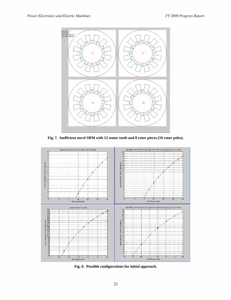
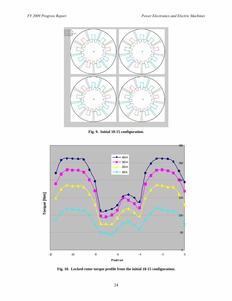
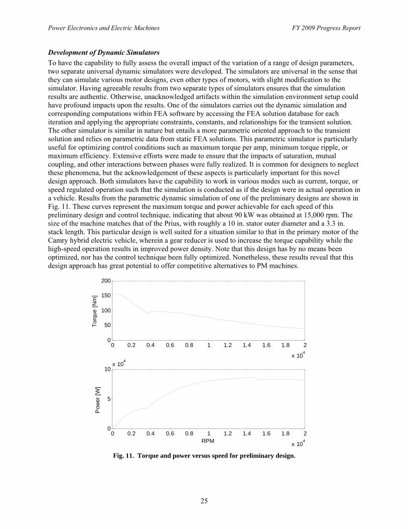
To reduce the complexity of the design in terms of the approach, simulation, and manufacturability, a wide-ranging evaluation technique was used to assess the various possibilities in which separate laminated pieces (example shown in Fig. 2) could be integrated into novel configurations. Initially, an assessment was made of the various possibilities for laminate piece use in the rotor, as shown in Fig. 7. The configuration shown in Fig. 7 is not entirely feasible but is merely an example of the initial approach. The lack of separation between the eight rotor pieces inherently leads to the presence of flux density in undesired paths, thereby reducing the saliency ratio and overall torque capability of the machine. A series of calculations was made to determine the separation between the pieces for various configurations, and the results are shown in Fig. 8. For the initial approach, the most clearly feasible configurations are a 15-9, 14-8, and 10-6, where the first number indicates the number of stator teeth and the second indicates the number of rotor pieces, where each rotor piece has two teeth. While these possibilities are feasible, there still exists some complexity in the rotor design in terms of manufacturability as well as complexity in the control and winding configuration. A more appealing approach is obtained when the stator and rotor configurations that were just described are interchanged, as the configurations become an 18-15, 16-14, and 12-10, respectively. In these cases, the rotor is of the same design as a conventional SRM, thereby alleviating concerns for cost, manufacturability, and reliability. A sketch of the 18-15 is shown in Fig. 9, wherein 9 stator pieces have 18 poles and a conventional 15 pole rotor is visible. Figure 10 shows the static torque curves obtained from FEA simulations for half of an electrical cycle. The natural torque production of the machine involves a significant overlapping of torque contribution from each phase. For the configuration in Fig. 10, two phases produce torque for four mechanical degrees (60 electrical), then one phase produces torque for four degrees during its maximum torque zone, then two phases again produce torque for the remaining four degrees. During this half electrical cycle, one phase remains active for the entire region. All of the machines of this type have torque characteristics similar to those of the 18-15. This approach inherently offers an opportunity to have greater control over torque ripple by means of current regulation. Based on the characteristics of the static torque curves of the initial design, it is apparent that if proper current regulation is applied during dynamic operation, torque ripple can be reduced to very low levels for low and moderate torque production. Although this technique will produce some benefit when applied to conventional SRMs, the inherent characteristics of the novel design approach more readily facilitate torque ripple levels below 5%. This is primarily because there are no zero or near-zero torque positions for the motor, as opposed to most conventional SRMs, which have sharp torque transients that approach zero. It is important to note that the static torque curves shown in Fig. 10 do not truly reflect the torque characteristics of the machine during dynamic operation, wherein inertia and inductance can introduce significant smoothing of the torque profile. More importantly, the design has significant room for optimization in terms of appropriately matching the torque, power, and speed requirements for each application. Additionally, detailed parametric studies will reveal more opportunities to manipulate the torque profile of the machine from a hardware design standpoint. Therefore a dynamic simulator is needed to fully realize all impacts of the design parameters.
Power Electronics and Electric Machines FY 2009 Progress Report
23
Fig. 7. Inefficient novel SRM with 12 stator teeth and 8 rotor pieces (16 rotor poles).
Fig. 8. Possible configurations for initial approach.
FY 2009 Progress Report Power Electronics and Electric Machines
24
Fig. 9. Initial 18-15 configuration.
Fig. 10. Locked-rotor torque profile from the initial 18-15 configuration.
To
rqu
e [N
m]
0
50
100
150
200
250
300
-12 -10 -8 -6 -4 -2 0
Posit i on
400 A
300 A
200 A
100 A
Power Electronics and Electric Machines FY 2009 Progress Report
25
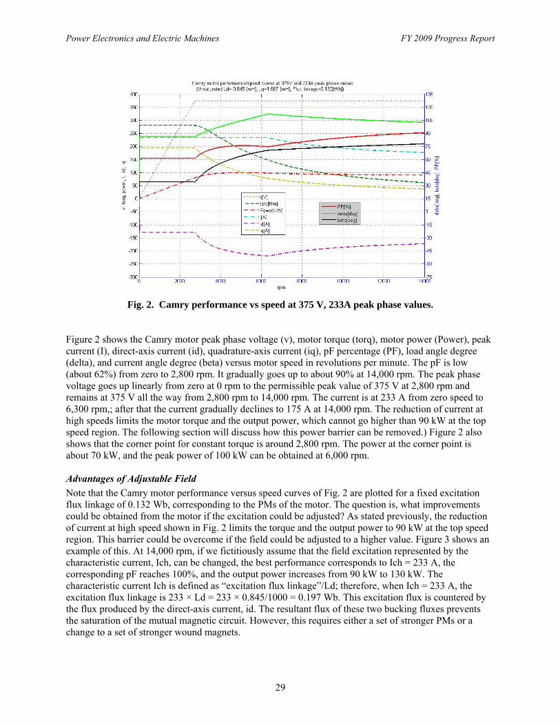
Development of Dynamic Simulators
To have the capability to fully assess the overall impact of the variation of a range of design parameters, two separate universal dynamic simulators were developed. The simulators are universal in the sense that they can simulate various motor designs, even other types of motors, with slight modification to the simulator. Having agreeable results from two separate types of simulators ensures that the simulation results are authentic. Otherwise, unacknowledged artifacts within the simulation environment setup could have profound impacts upon the results. One of the simulators carries out the dynamic simulation and corresponding computations within FEA software by accessing the FEA solution database for each iteration and applying the appropriate constraints, constants, and relationships for the transient solution. The other simulator is similar in nature but entails a more parametric oriented approach to the transient solution and relies on parametric data from static FEA solutions. This parametric simulator is particularly useful for optimizing control conditions such as maximum torque per amp, minimum torque ripple, or maximum efficiency. Extensive efforts were made to ensure that the impacts of saturation, mutual coupling, and other interactions between phases were fully realized. It is common for designers to neglect these phenomena, but the acknowledgement of these aspects is particularly important for this novel design approach. Both simulators have the capability to work in various modes such as current, torque, or speed regulated operation such that the simulation is conducted as if the design were in actual operation in a vehicle. Results from the parametric dynamic simulation of one of the preliminary designs are shown in Fig. 11. These curves represent the maximum torque and power achievable for each speed of this preliminary design and control technique, indicating that about 90 kW was obtained at 15,000 rpm. The size of the machine matches that of the Prius, with roughly a 10 in. stator outer diameter and a 3.3 in. stack length. This particular design is well suited for a situation similar to that in the primary motor of the Camry hybrid electric vehicle, wherein a gear reducer is used to increase the torque capability while the high-speed operation results in improved power density. Note that this design has by no means been optimized, nor has the control technique been fully optimized. Nonetheless, these results reveal that this design approach has great potential to offer competitive alternatives to PM machines.
0 0.2 0.4 0.6 0.8 1 1.2 1.4 1.6 1.8 2
x 104
0
50
100
150
200
Tor
que
[Nm
]
0 0.2 0.4 0.6 0.8 1 1.2 1.4 1.6 1.8 2
x 104
0
5
10x 10
4
Pow
er [
W]
RPM
Fig. 11. Torque and power versus speed for preliminary design.

FY 2009 Progress Report Power Electronics and Electric Machines
26
Conclusions • Maintained low manufacturing and fabrication costs of conventional SRM. • Maintained robustness of conventional SRM. • Demonstrated through simulations a significant reduction of torque ripple versus conventional SRM. • Matched or surpassed performance of conventional SRM. • Design approach created the opportunity to greatly reduce acoustic noise and vibration from a
structural and magnetic standpoint. • Demonstrated continuous conduction operation. Publications None. References None. Patents None.

Power Electronics and Electric Machines FY 2009 Progress Report
27
3.2 Novel Flux Coupling Machine without Permanent Magnets
Principal Investigator: John S. Hsu Team Member: Randy Wiles Oak Ridge National Laboratory National Transportation Research Center 2360 Cherahala Boulevard Knoxville, TN 37932 Voice: 865-946-1325; Fax: 865-946-1262; E-mail: [email protected] DOE Technology Development Manager: Susan A. Rogers Voice: 202-586-8997; Fax: 202-586-1600; E-mail: [email protected] ORNL Program Manager: Mitch Olszewski Voice: 865-946-1350; Fax: 865-946-1262; E-mail: [email protected] Objectives • Research the feasibility of an electric motor, without permanent magnets (PMs), that has the potential
to replace the internal PM (IPM) motor in hybrid electric vehicles and plug-in hybrid electric vehicles.
• Produce a motor that meets or exceeds DOE’s 2020 motor targets for cost, weight, volume, and efficiency.
Approach Identify the advantages and weaknesses of the most advanced IPM motors available in the market today and use this information to develop a motor which retains the advantages of IPM motors without the use of rare earth PMs. Major Accomplishments • Identified the advantages and disadvantages of IPM motors.
— The following are among the advantages of IPM motors. 1. They are compact, possessing high power density. 2. They have good starting torque.
— The following are among the weaknesses of IPM motors.
1. Cost. The cost of IPM motors will likely go up due to supply and demand factors impacting the rare earth elements used in the PMs.
2. Temperature limitations of PMs prevent higher operating temperatures. 3. Speed limitations. Larger bridges are necessary to maintain mechanical integrity at high
speeds. Larger bridges provide a pathway for flux leakage, resulting in poor performance. 4. Low power factor (pF). This is due to the fixed strength of PMs when operating in a broad
speed and load region. This lower pF reduces the power output of the motor at given current and voltage limits. It also increases the load on the power electronic switching devices.
5. Saturated and unsaturated inductance values of the direct and quadrature axes (Ld and Lq, respectively) change significantly at different loads; thus, fixed PMs are not always optimized for these variable inductance values.
6. Power levels cannot be increased at higher speeds due to the limitation of PMs under given voltage and current values.

FY 2009 Progress Report Power Electronics and Electric Machines
28
7. The flux field produced by PMs cannot be cut off — To prevent core losses at higher speeds. This also occurs even when the motor is
disconnected from the power supply. — To prevent a defective motor’s winding short-circuiting (again, this occurs even when the
motor is disconnected from the power supply). • Completed the development of analytical tools used for the design of the Novel Flux Coupling
Machine without PMs. • Completed electromagnetic simulations for motor performance and mechanical finite element
analysis for rotational stress loading (80% complete). Future Direction • Enhance the design to reduce the size of the motor. • Analyze the feasibility of incorporating low cost PMs such as Alnico or ferrite. Determine whether
these low cost PMs will enhance the motor’s capabilities. Technical Discussion The following technical discussion shows three dimensional (3D) finite element results and analytical plots obtained through the ANSYS, ANSOFT, ALGOR, COMSOL, and MATLAB software. The analytical equations were derived by ORNL. Power Factor of Internal PM Motors
There is a common misconception that IPM motor pFs are always high because of the PMs. This misconception can be clarified with an example from classical V-curve theory. Figure 1 shows a set of typical pF curves for different loads of a synchronous motor at different field excitation selected from the horizontal field current axis and from various armature currents indicated by the vertical axis. When the motor has a given field excitation such as a fixed PM excitation selected from the equivalent field current axis, the corresponding pF obtained from the curves would change at different loads. A good 100% pF can be obtained at any load if the field can be adjusted over a sufficiently wide range. For an IPM motor there is always a set of V curves corresponding to each set of given speed and terminal voltages; an optimal pF can be obtained by adjusting the field excitation.
Fig. 1. Classical V curves.
The misconception of a high pF in IPMs can be further clarified through the analytical performance plots of a Camry IPM motor (Fig. 2).
Power Electronics and Electric Machines FY 2009 Progress Report
29
Fig. 2. Camry performance vs speed at 375 V, 233A peak phase values. Figure 2 shows the Camry motor peak phase voltage (v), motor torque (torq), motor power (Power), peak current (I), direct-axis current (id), quadrature-axis current (iq), pF percentage (PF), load angle degree (delta), and current angle degree (beta) versus motor speed in revolutions per minute. The pF is low (about 62%) from zero to 2,800 rpm. It gradually goes up to about 90% at 14,000 rpm. The peak phase voltage goes up linearly from zero at 0 rpm to the permissible peak value of 375 V at 2,800 rpm and remains at 375 V all the way from 2,800 rpm to 14,000 rpm. The current is at 233 A from zero speed to 6,300 rpm,; after that the current gradually declines to 175 A at 14,000 rpm. The reduction of current at high speeds limits the motor torque and the output power, which cannot go higher than 90 kW at the top speed region. The following section will discuss how this power barrier can be removed.) Figure 2 also shows that the corner point for constant torque is around 2,800 rpm. The power at the corner point is about 70 kW, and the peak power of 100 kW can be obtained at 6,000 rpm. Advantages of Adjustable Field
Note that the Camry motor performance versus speed curves of Fig. 2 are plotted for a fixed excitation flux linkage of 0.132 Wb, corresponding to the PMs of the motor. The question is, what improvements could be obtained from the motor if the excitation could be adjusted? As stated previously, the reduction of current at high speed shown in Fig. 2 limits the torque and the output power to 90 kW at the top speed region. This barrier could be overcome if the field could be adjusted to a higher value. Figure 3 shows an example of this. At 14,000 rpm, if we fictitiously assume that the field excitation represented by the characteristic current, Ich, can be changed, the best performance corresponds to Ich = 233 A, the corresponding pF reaches 100%, and the output power increases from 90 kW to 130 kW. The characteristic current Ich is defined as “excitation flux linkage”/Ld; therefore, when Ich = 233 A, the excitation flux linkage is 233 × Ld = 233 × 0.845/1000 = 0.197 Wb. This excitation flux is countered by the flux produced by the direct-axis current, id. The resultant flux of these two bucking fluxes prevents the saturation of the mutual magnetic circuit. However, this requires either a set of stronger PMs or a change to a set of stronger wound magnets.

FY 2009 Progress Report Power Electronics and Electric Machines
30
Fig. 3. Sweeping excitation of Camry motor for higher power within current and voltage limits at 14,000 rpm.
Conceptual Geometry of a Novel Flux Coupling Machine without PMs
Figure 4 shows a conceptualization of the Novel Flux Coupling Machine without PMs. It consists of a wound stator core; two stationary excitation toroidal coils; two stationary end brackets that house the bearings; the toroidal coils, which serve as flux paths for exciting the rotor; and a rotor. The rotor is made of lamination punchings, rotor hub, and end plates. There are no PMs in the rotor; the cavities vacated by the PMs are used for locating the mechanical enforcing components. The bridges are narrow for reducing the leakage fluxes. The radial air gap is 0.78 mm per side, and the axial air gap is 1.5 mm per side. Figure 5 shows that the axial distance between end brackets of the Camry motor is 202 mm. Figure 6 shows the volume comparison between the Camry motor and the concept novel flux coupling motor by placing the latter in the space between the Camry end brackets. There are cross-sectional area deficits for the novel flux coupling motor, indicating the work needed to further reduce the motor’s volume. The volume of the motor as currently envisioned is not excessively larger than the Camry motor; however, it would be expected that the motor would be heavier than the Camry motor due to the greater amount of iron in it. The parts weight of the Novel Flux Coupling Machine is 115 lb. The motor would be heavier than the Camry motor due to the two 32 lb steel end brackets. Thus if the weight cannot be tolerated, the motor must be designed using a low iron approach (i.e., less flux and higher turns of stator winding) and be developed for a higher speed than the IPM motor. Alternatively, a low cost PM-assisted motor could be developed to reduce the weight of the steel end brackets.
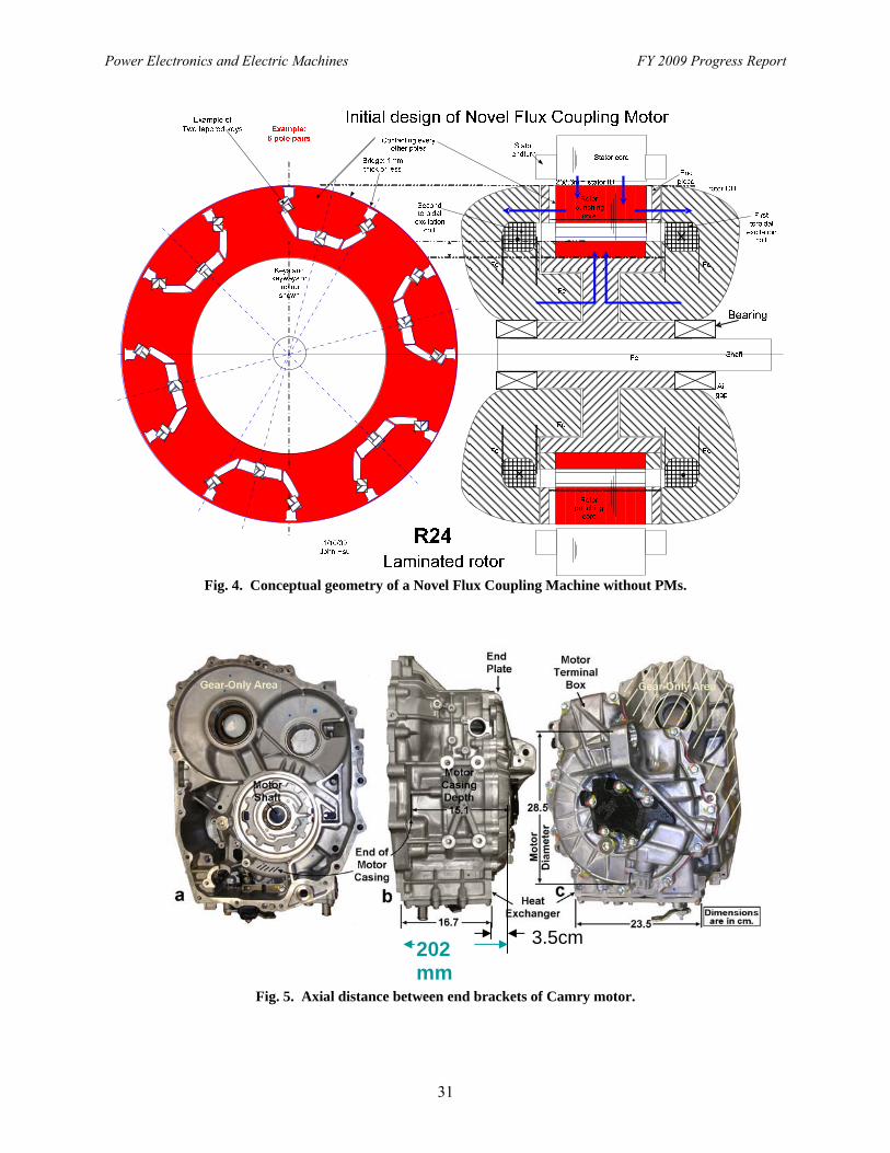
Power Electronics and Electric Machines FY 2009 Progress Report
31
Fig. 4. Conceptual geometry of a Novel Flux Coupling Machine without PMs.
Fig. 5. Axial distance between end brackets of Camry motor.
3.5cm 202 mm
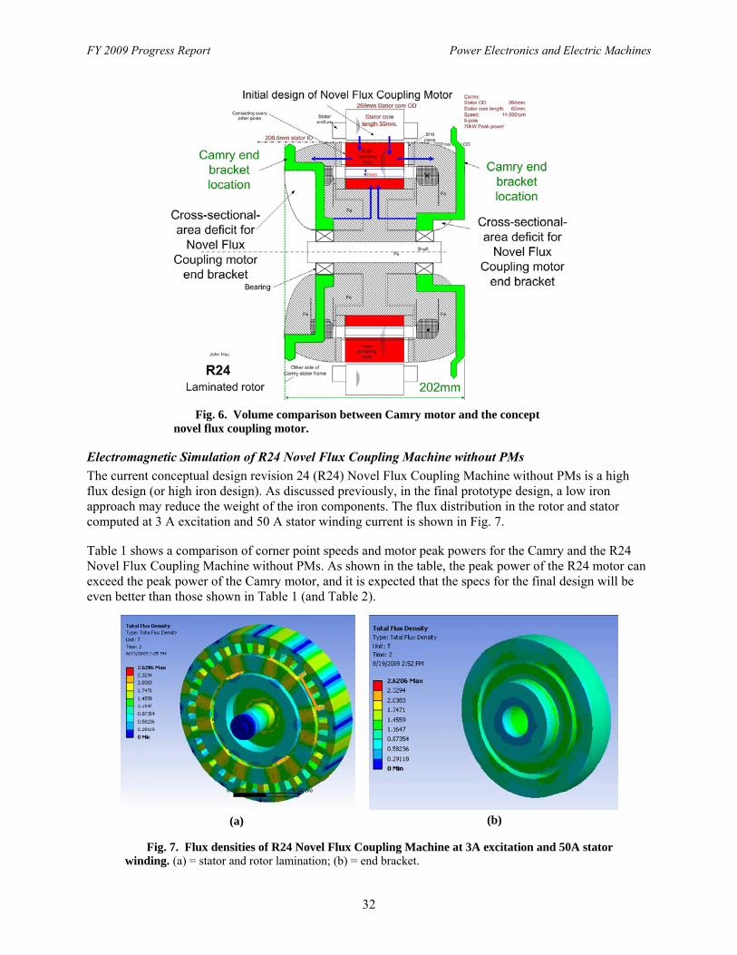
FY 2009 Progress Report Power Electronics and Electric Machines
32
Fig. 6. Volume comparison between Camry motor and the concept novel flux coupling motor.
Electromagnetic Simulation of R24 Novel Flux Coupling Machine without PMs
The current conceptual design revision 24 (R24) Novel Flux Coupling Machine without PMs is a high flux design (or high iron design). As discussed previously, in the final prototype design, a low iron approach may reduce the weight of the iron components. The flux distribution in the rotor and stator computed at 3 A excitation and 50 A stator winding current is shown in Fig. 7. Table 1 shows a comparison of corner point speeds and motor peak powers for the Camry and the R24 Novel Flux Coupling Machine without PMs. As shown in the table, the peak power of the R24 motor can exceed the peak power of the Camry motor, and it is expected that the specs for the final design will be even better than those shown in Table 1 (and Table 2).
Fig. 7. Flux densities of R24 Novel Flux Coupling Machine at 3A excitation and 50A stator winding. (a) = stator and rotor lamination; (b) = end bracket.
(a) (b)

Power Electronics and Electric Machines FY 2009 Progress Report
33
Table 1. Comparison of corner-point speeds and motor peak powers
Corner-point speed (rpm)
Peak power (Kw)
Camry 4,500 (claimed) 105 (claimed) (disputed to be 70kW)
R24 motor
3,987 Calculated @ 10A excitation
288 Nm*3,987 rpm*2*pi/60 = 120
5,579 Calculated @ 60% excitation flux 182 Nm*5,579 rpm*2*pi/60 = 106
Excitation Power Required for R24 Novel Flux Coupling Machine without PMs
Table 2 shows the simulated torque of the R24 motor at different stator winding phase currents and excitation currents. During normal operation the excitation current would be around 3 A.
Table 2. Torque Versus Phase Current and Excitation Current
Phase current (Arm)
Excitation current (Adc)
Torque (Nm)
300 10 307 300 3 192 233 5 242 141 10 246 141 3 150
The required excitation power is inversely proportional to the available area of the excitation coil. Table 3 shows two available coil areas; one is a little less than 0.5 in.2, and the second one is slightly less than 1 in.2. The power consumed by the excitation coil at 3A and 200°C is 445 W and 159 W for the two available coil areas, respectively. The R24 motor’s efficiency will be reduced by1% during normal operation. For a 100 kW motor, this would be 1 kW. The excitation loss can be significantly reduced if the available coil area can be increased from 0.5 in.2.
Table 3. Excitation current, voltage, and power of R24 novel motor
Available coil area per side
(mm)
Net copper area per side (mm2) (0.8 fill factor)
Resistancea of 850-turn coil with 132 mm average
diameter
Resistancea of coil
at 200°C
Voltage at 10A and at 200°C
(Vdc)
Voltage at 3A and at 200°C
(Vdc)
Power at 3A and at 200°C
per coil (W)
16 × 18 (288 mm2)
230 22.4 (at 20°C)
38.2 382 115 445
25 × 25 (625 mm2)
500 10.3 (at 20°C)
17.6 176 53 159
aResistance in ohms.
Performance/Speed Curves of R24 Novel Flux Coupling Machine
The following two sets of performance versus speed curves show the differences corresponding to saturated inductances of Ld and Lq at the different flux linkage values that are produced by the adjustable field excitation. Ideally the inductances and the flux linkage values would be simulated for each point of the curves. Unfortunately, it takes more than 10 h to conduct one run for the 3D simulation, and this expenditure of time was not deemed to be justified at this conceptual design stage. To compensate, two excitation flux linkages, 0.132 and 0.09 Wb, were used to see their influences.
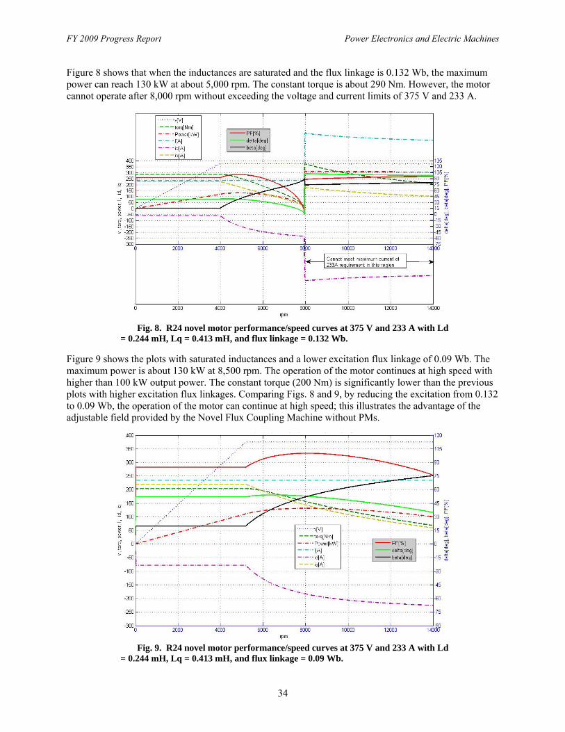
FY 2009 Progress Report Power Electronics and Electric Machines
34
Figure 8 shows that when the inductances are saturated and the flux linkage is 0.132 Wb, the maximum power can reach 130 kW at about 5,000 rpm. The constant torque is about 290 Nm. However, the motor cannot operate after 8,000 rpm without exceeding the voltage and current limits of 375 V and 233 A.
Fig. 8. R24 novel motor performance/speed curves at 375 V and 233 A with Ld
= 0.244 mH, Lq = 0.413 mH, and flux linkage = 0.132 Wb.
Figure 9 shows the plots with saturated inductances and a lower excitation flux linkage of 0.09 Wb. The maximum power is about 130 kW at 8,500 rpm. The operation of the motor continues at high speed with higher than 100 kW output power. The constant torque (200 Nm) is significantly lower than the previous plots with higher excitation flux linkages. Comparing Figs. 8 and 9, by reducing the excitation from 0.132 to 0.09 Wb, the operation of the motor can continue at high speed; this illustrates the advantage of the adjustable field provided by the Novel Flux Coupling Machine without PMs.
Fig. 9. R24 novel motor performance/speed curves at 375 V and 233 A with Ld
= 0.244 mH, Lq = 0.413 mH, and flux linkage = 0.09 Wb.
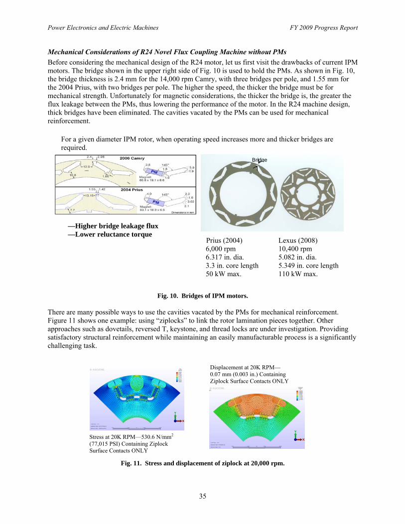
Power Electronics and Electric Machines FY 2009 Progress Report
35
Mechanical Considerations of R24 Novel Flux Coupling Machine without PMs
Before considering the mechanical design of the R24 motor, let us first visit the drawbacks of current IPM motors. The bridge shown in the upper right side of Fig. 10 is used to hold the PMs. As shown in Fig. 10, the bridge thickness is 2.4 mm for the 14,000 rpm Camry, with three bridges per pole, and 1.55 mm for the 2004 Prius, with two bridges per pole. The higher the speed, the thicker the bridge must be for mechanical strength. Unfortunately for magnetic considerations, the thicker the bridge is, the greater the flux leakage between the PMs, thus lowering the performance of the motor. In the R24 machine design, thick bridges have been eliminated. The cavities vacated by the PMs can be used for mechanical reinforcement.
Fig. 10. Bridges of IPM motors.
There are many possible ways to use the cavities vacated by the PMs for mechanical reinforcement. Figure 11 shows one example: using “ziplocks” to link the rotor lamination pieces together. Other approaches such as dovetails, reversed T, keystone, and thread locks are under investigation. Providing satisfactory structural reinforcement while maintaining an easily manufacturable process is a significantly challenging task.
Fig. 11. Stress and displacement of ziplock at 20,000 rpm.
Stress at 20K RPM—530.6 N/mm2
(77,015 PSI) Containing Ziplock Surface Contacts ONLY
Displacement at 20K RPM—0.07 mm (0.003 in.) Containing Ziplock Surface Contacts ONLY
Prius (2004) Lexus (2008) 6,000 rpm 10,400 rpm 6.317 in. dia. 5.082 in. dia. 3.3 in. core length 5.349 in. core length 50 kW max. 110 kW max.
Bridge
For a given diameter IPM rotor, when operating speed increases more and thicker bridges are required.
—Higher bridge leakage flux —Lower reluctance torque

FY 2009 Progress Report Power Electronics and Electric Machines
36
Target Review (Table 4)
Because the Camry IPM motor is close to meeting DOE’s 2020 targets (except that the cost, $10.7/kW versus the $4.7/kW target, is high and the permissible temperature rating, 65°C coolant versus 105°C coolant target, is low), we have used the Camry motor as a point of reference for the R24 motor design. The R24 design features removing the rare earth PMs to lower the cost, increasing the motor permissible operating temperature, and increasing the permissible speed for size and weight reduction. With the R24 machine design, the power output of the motor can be higher than that of the Camry motor. Additionally, the permissible temperature can be higher, and the volume is close to the volume between the Camry end brackets. The R24 motor is heavier than the Camry motor because the end brackets are made of iron instead of aluminum.
Table 4. DOE Targets
Traction drive system Power electronics Motor
$/kW kW/kg kW/L Efficiency
Coolanttemp.(°C) $/kW kW/$ kW/kg kW/L $/kW kW/$ kW/kg kW/L
Camry 36.6 1.2 3.2 65 25.9 4.3 7.1 10.7 1.7 4.73 Camry (est.) 73.1 0.6 1.6 89 105 51.7 0.019 2.2 3.5 21.4 0.047 0.9 2.9
Targets
2010 19 1.06 2.6 90 90 7.9 10.8 8.7 11.1 0.09 1.2 3.7
2015 12 1.2 3.5 93 105 5 0.20 12 12 7 0.143 1.3 5 2020 8 1.4 4 94 105 3.3 0.30 14.1 13.4 4.7 0.213 1.6 5.7
Summary of FY 2009 Novel Flux Coupling Machine Work • Computations show the R24 Novel Flux Coupling Machine without PMs has good potential for
meeting the DOE 2020 targets. • Further work remains to reduce the R24 machine size and weight.
Comparative assessment of the R24 Novel Flux Coupling Machine without PMs shows the following. • Permissible rotor speed can increase without thick bridges for PM retention. • Permissible temperature can be higher without the limitations of PMs. • pF and performance can increase with adjustable field control. • Load can affect Ld and Lq values of IPMs as well as the R24 motor due to magnetic saturation; the
adjustable field can help achieve the best performance. • Motor size is comparable to the Camry motor. • Mild steel (or equivalent) motor brackets are required, which adds weight to the motor.

Power Electronics and Electric Machines FY 2009 Progress Report
37
4. Power Electronics Research and Technology Development
4.1 Wide Bandgap Materials
Principal Investigator: Madhu Sudhan Chinthavali Oak Ridge National Laboratory National Transportation Research Center 2360 Cherahala Boulevard Knoxville, TN 37932 Voice: 865-946-1411; Fax: 865-946-1262; E-mail:[email protected] DOE Technology Development Manager: Susan A. Rogers Voice: 202-586-8997; Fax: 202-586-1600; E-mail: [email protected] ORNL Program Manager: Mitch Olszewski Voice: 865-946-1350; Fax: 865-946-1262; E-mail: [email protected] Objectives • To keep up-to-date with state-of-the-art wide bandgap (WBG) power devices and acquire, test, and
characterize new WBG power devices. • To study the feasibility of an air-cooled 55 kW inverter. Approach • Acquire, test, and characterize new WBG power devices. Analysis includes the following.
— Static characteristic tests. — Dynamic characteristic tests. — Behavioral modeling.
• Perform a feasibility study on an air-cooled inverter concept. The tasks include the following. — Conduct research on new packaging techniques. — Develop inverter designs and model them to evaluate the thermal performance through
conduction analysis. — Design air flow patterns and simulate the inverter design to assess the feasibility.
Major Accomplishments • Acquired, tested, and characterized silicon carbide (SiC) junction field-effect transistors (JFETs),
metal-oxide semiconductor field-effect transistors (MOSFETs), and diodes. • Completed evaluation of a 10 kW SiC JFET-based inverter. • Completed the feasibility study of an air-cooled 55 kW inverter design. Future Direction • State-of-the-art WBG power devices will be acquired, tested, and characterized. • Test data will be used to develop SPICE (Simulation Program with Integrated Circuit Emphasis)
models of the devices to aid in ORNL packaging efforts.
FY 2009 Progress Report Power Electronics and Electric Machines
38
Technical Discussion
I. Device Testing WBG devices acquired this year were SiC MOSFETs, normally off SiC JFETs, and SiC Schottky diodes. These devices were tested and characterized. The test results for these devices will be presented in the following sections. All the devices obtained were experimental samples. 1. SiC MOSFET Static Characteristics
Static characteristics of a 1,200 V, 100 A SiC MOSFET in a half bridge module are shown in Fig. 1 for different operating temperatures at 20 V gate-source voltage (Vgs). This module is built using the commercial Si CM100DY-24A half bridge module package. At 15 V Vgs, the on-resistance initially decreased from 0.0194 Ω at 20°C to 0.0161 Ω at 100°C and then started to increase up to 0.0183 Ω at 175°C, as shown in Fig. 2. This behavior was noticed in the low amperage MOSFETs tested at ORNL in 2005. However, at 20 V Vgs the on-resistance increased from 0.0134 Ω at 20°C to 0.0162 Ω at 175°C. There is a significant change in the forward characteristics of the device at different gate voltages. This will affect the paralleling of the device for high-power modules.
0 0.2 0.4 0.6 0.8 1 1.2 1.4 1.6 1.80
10
20
30
40
50
60
70
80
90
100
110
Drain-Source Voltage drop (V)
Dra
in C
urr
ent
(A)
Increasing Temperature(25 C to 175 C)
Fig. 1. Current-voltage (I-V) curves of a 1,200 V, 100 A SiC MOSFET.
Dynamic Characteristics
The SiC MOSFET was tested in a chopper circuit with double pulse switching to observe its dynamic characteristics. The double pulse circuit enables the use of an inductive load alone instead of the resistive and inductive load together. The current through the inductor builds up during the first pulse and peak forward current is adjusted by changing the width of the first pulse. The switch is turned off and turned on for short periods after the first pulse. The turn-on and turn-off energy losses can be obtained during the short pulse intervals. The gate driver used for obtaining the dynamic characteristics is a commercial gate driver (HCPL 316J). The gate voltage was switched from +15 V Vgs to -5 V Vgs. The diode in the half bridge module was used as the clamping diode with a 110 µH inductor as the load. The turn-on and turn-off energy losses of the MOSFET at 300 V and 50 A are shown in Table 1. The turn-on losses and turn-off losses do not change much with temperature.
Power Electronics and Electric Machines FY 2009 Progress Report
39
20 40 60 80 100 120 140 160 1800.013
0.014
0.015
0.016
0.017
0.018
0.019
0.02
0.021
0.022
0.023
Temperature (C)
Res
ista
nce
(m
oh
m)
,
Vgs 15V
Vgs 20V
Fig. 2. On-state resistance of a 1,200 V, 100 A SiC MOSFET.
Table 1. Switching Energy Losses of SiC MOSFET
Temp (°C)
Eon (mJ)
Eoff (mJ)
Etot (mJ)
25 1.0544 1.0304 2.0848
100 1.1138 1.0344 2.1482
150 1.1318 1.0694 2.2012
2. SiC 1,200V, 100 A JBS diode Static Characteristics The static characteristics of a 1,200 V, 100 A SiC junction barrier Schottky (JBS) diode in the SiC MOSFET module were obtained across a wide temperature range (25°C–200°C) (Fig. 3). The forward voltage drop at 100 A current increased from 1.71 V at 25°C to 2.53 V at 200°C. The on-state voltage drop decreased from 0.78 at 25°C to 0.5014 at 200°C, as shown in Fig. 4. The on-state resistance increased from 0.0077 Ω at 25°C to 0.0176 Ω at 200°C for currents greater than 20 A. It should be noted that the diode has negative temperature coefficient below 20 A current. Dynamic Characteristics
The SiC JBS diode was tested in the same chopper circuit as the SiC MOSFET with double pulse switching to observe its dynamic characteristics. The turn-off energy losses of the JBS diode at 300 V and 50 A are shown in Table 2. The turn-off losses do not change much with temperature, exhibiting temperature independent switching loss behavior.
FY 2009 Progress Report Power Electronics and Electric Machines
40
0 0.5 1 1.5 2 2.50
10
20
30
40
50
60
70
80
90
100
On-state Voltage(V)
Cu
rren
t (A
)
Increasing Temperature(25C to 200C)
Fig. 3. I-V curves of a SiC 1,200 V, 100 A JBS diode.
20 40 60 80 100 120 140 160 180 200 2200.45
0.5
0.55
0.6
0.65
0.7
0.75
0.8
On
-sta
te v
olt
age
dro
p (
V)
20 40 60 80 100 120 140 160 180 200 2200.006
0.008
0.01
0.012
0.014
0.016
0.018
0.02
Temperature (C)
On
-sta
te r
esis
tan
ce (
Oh
ms)
Fig. 4. On-resistance and on-state voltage of a SiC
1,200 V, 100 A JBS diode.
Table 2. Switching Energy Losses of 1,200 V, 100 A SiC JBS Diode
Temp (°C)
Eoff (mJ)
25 2.47
100 2.65
150 2.71
3. Normally off 1,200 V, 10 A SiC JFET Static Characteristics
Static characteristics of a 1,200 V, 10 A normally off SiC JFET are shown in Fig. 5 for different operating temperatures. Normally off devices are the preferred type of devices in power converters for fail-safe operation. The forward characteristics were obtained for a gate voltage of 3 V. The on-resistance of the JFET increases from 0.093 Ω at 25°C to 0.2 Ω at 150°C and hence has a positive temperature coefficient (Fig. 6).
Power Electronics and Electric Machines FY 2009 Progress Report
41
0 0.2 0.4 0.6 0.8 1 1.2 1.4 1.60
1
2
3
4
5
6
7
8
9
10
11
Voltage (V)
Cu
rre
nt(
A)
Increasing Temperature(25 C to 150C)
Fig. 5. I-V curves of a 1,200 V, 10 A normally off
SiC JFET.
20 40 60 80 100 120 140 1600.08
0.1
0.12
0.14
0.16
0.18
0.2
On
-res
ista
nce
(O
hm
s)
Temperature (C) Fig. 6. On-resistance of a 1,200 V, 10 A normally
off SiC JFET.
Dynamic Characteristics
The turn-on and turn-off energy losses of the 1,200 V, 10 A normally off SiC JFET were obtained using the double pulse circuit with a load inductance of 110 µH, and a 600 V, 10 A Cree Schottky diode was used as the clamping diode in the chopper circuit. The effect of the diode on the SiC JFET will be minimal because of the almost zero reverse recovery current of the diode. The gate drive used for the test was a commercial IDD414PI IXYS chip with 35 V, 14 A output drive capability. The device requires constant current to remain switched on, and this features demands more power from the gate driver. The data were obtained at 600 V dc for various currents at 25°C and 150°C. The total energy losses increase with an increase in current; however, the losses do not change much with increases in temperature (Fig. 7).
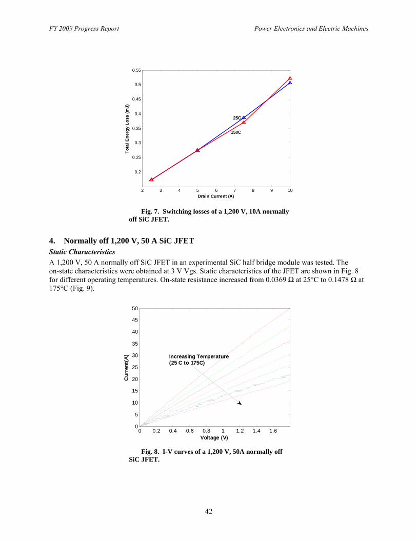
FY 2009 Progress Report Power Electronics and Electric Machines
42
2 3 4 5 6 7 8 9 10
0.2
0.25
0.3
0.35
0.4
0.45
0.5
0.55
Drain Current (A)
To
tal
En
erg
y L
oss
(m
J)
25C
150C
Fig. 7. Switching losses of a 1,200 V, 10A normally off SiC JFET.
4. Normally off 1,200 V, 50 A SiC JFET Static Characteristics
A 1,200 V, 50 A normally off SiC JFET in an experimental SiC half bridge module was tested. The on-state characteristics were obtained at 3 V Vgs. Static characteristics of the JFET are shown in Fig. 8 for different operating temperatures. On-state resistance increased from 0.0369 Ω at 25°C to 0.1478 Ω at 175°C (Fig. 9).
0 0.2 0.4 0.6 0.8 1 1.2 1.4 1.60
5
10
15
20
25
30
35
40
45
50
Voltage (V)
Cu
rre
nt(
A) Increasing Temperature
(25 C to 175C)
Fig. 8. I-V curves of a 1,200 V, 50A normally off SiC JFET.
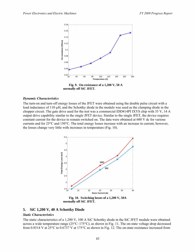
Power Electronics and Electric Machines FY 2009 Progress Report
43
20 40 60 80 100 120 140 160 1800.02
0.04
0.06
0.08
0.1
0.12
0.14
0.16
0.18
On
-res
ista
nce
(O
hm
s)
Temperature (C) Fig. 9. On-resistance of a 1,200 V, 50 A
normally off SiC JFET.
Dynamic Characteristics
The turn-on and turn-off energy losses of the JFET were obtained using the double pulse circuit with a load inductance of 110 µH, and the Schottky diode in the module was used as the clamping diode in the chopper circuit. The gate drive used for the test was a commercial IDD414PI IXYS chip with 35 V, 14 A output drive capability similar to the single JFET device. Similar to the single JFET, the device requires constant current for the device to remain switched on. The data were obtained at 600 V dc for various currents and for 25°C and 150°C. The total energy losses increase with an increase in current; however, the losses change very little with increases in temperature (Fig. 10).
10 15 20 25 30 35 401.5
2
2.5
3
3.5
4
4.5
5
5.5
Drain Current (A)
To
tal
En
erg
y L
oss
(m
J)
25C
150C
Fig. 10. Switching losses of a 1,200 V, 50A
normally off SiC JFET. 5. SiC 1,200 V, 40 A Schottky Diode Static Characteristics
The static characteristics of a 1,200 V, 100 A SiC Schottky diode in the SiC JFET module were obtained across a wide temperature range (25°C–175°C), as shown in Fig. 11. The on-state voltage drop decreased from 0.8514 V at 25°C to 0.6737 V at 175°C as shown in Fig. 12. The on-state resistance increased from
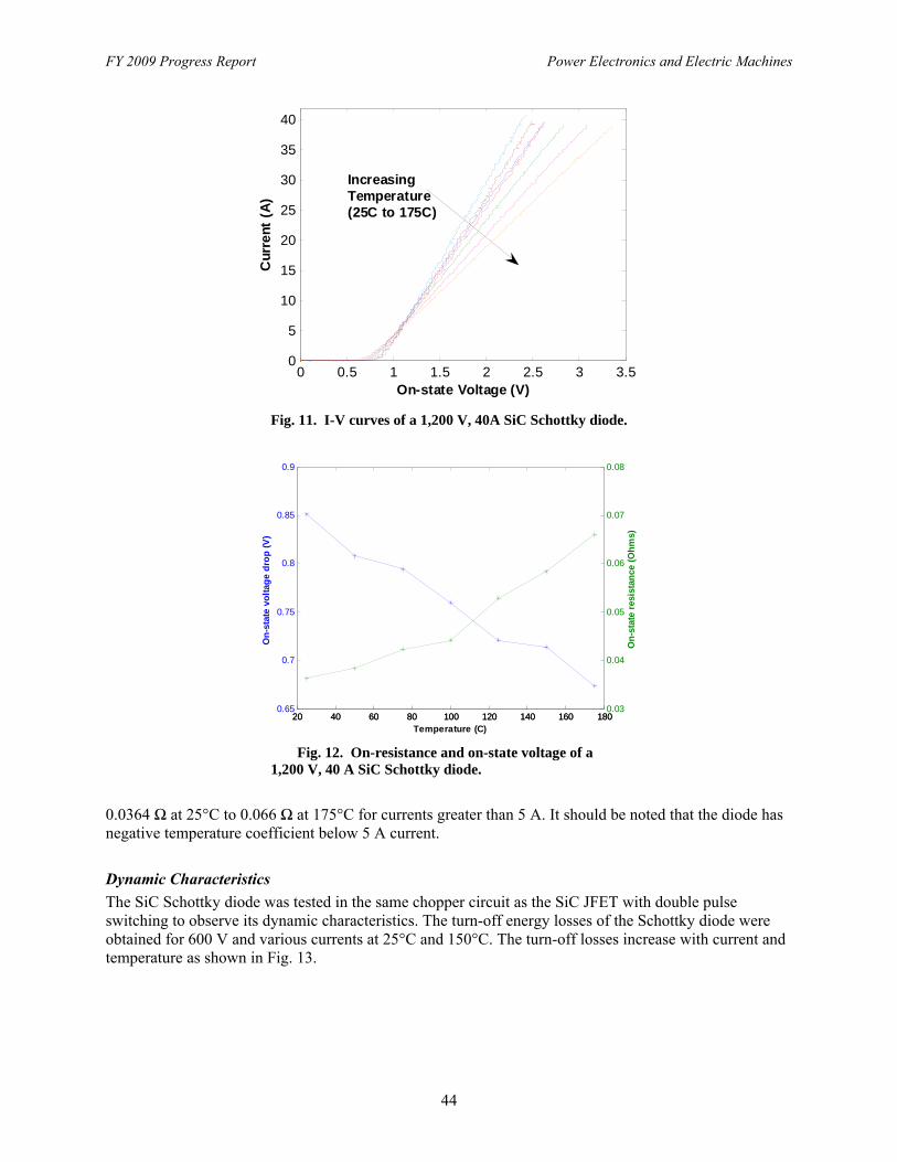
FY 2009 Progress Report Power Electronics and Electric Machines
44
Fig. 11. I-V curves of a 1,200 V, 40A SiC Schottky diode.
Fig. 12. On-resistance and on-state voltage of a 1,200 V, 40 A SiC Schottky diode.
0.0364 Ω at 25°C to 0.066 Ω at 175°C for currents greater than 5 A. It should be noted that the diode has negative temperature coefficient below 5 A current.
Dynamic Characteristics
The SiC Schottky diode was tested in the same chopper circuit as the SiC JFET with double pulse switching to observe its dynamic characteristics. The turn-off energy losses of the Schottky diode were obtained for 600 V and various currents at 25°C and 150°C. The turn-off losses increase with current and temperature as shown in Fig. 13.
0 0.5 1 1.5 2 2.5 3 3.50
5
10
15
20
25
30
35
40
On-state Voltage (V)
Cu
rre
nt
(A)
IncreasingTemperature(25C to 175C)
20 40 60 80 100 120 140 160 1800.65
0.7
0.75
0.8
0.85
0.9
On
-sta
te v
olt
age
dro
p (
V)
20 40 60 80 100 120 140 160 1800.03
0.04
0.05
0.06
0.07
0.08
Temperature (C)
On
-sta
te r
esis
tan
ce (
Oh
ms)
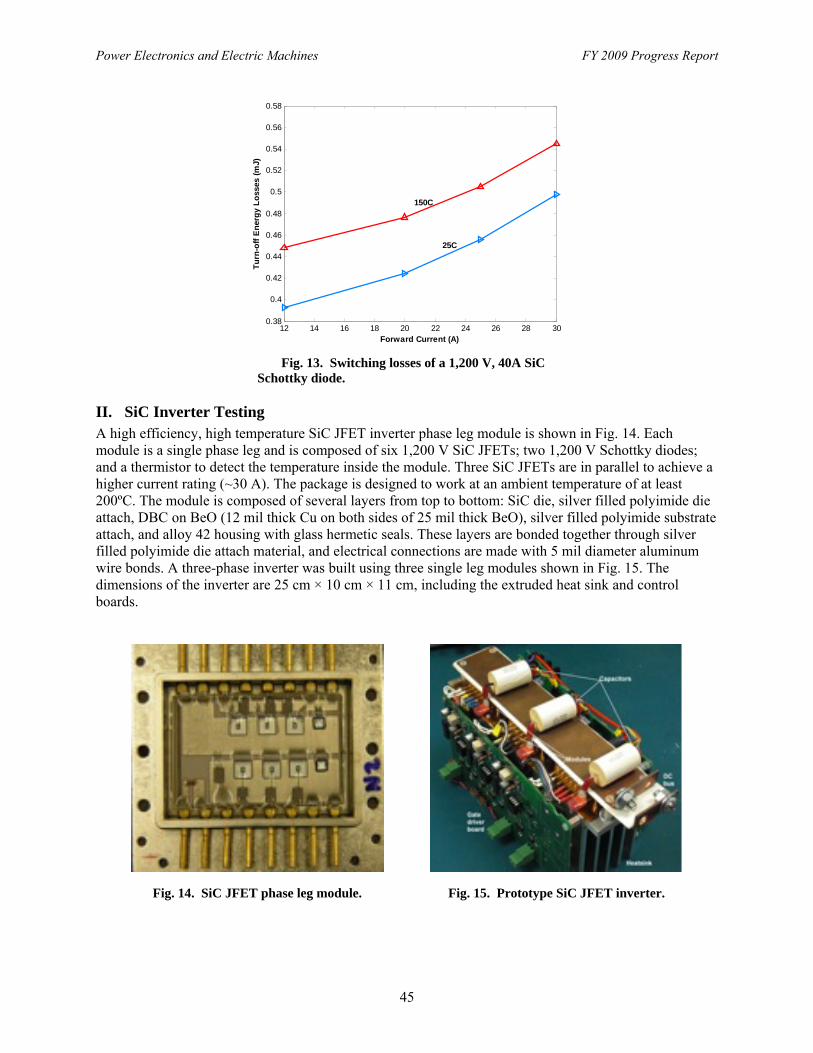
Power Electronics and Electric Machines FY 2009 Progress Report
45
12 14 16 18 20 22 24 26 28 300.38
0.4
0.42
0.44
0.46
0.48
0.5
0.52
0.54
0.56
0.58
Forward Current (A)
Tu
rn-o
ff E
ner
gy
Lo
sses
(m
J)25C
150C
Fig. 13. Switching losses of a 1,200 V, 40A SiC
Schottky diode. II. SiC Inverter Testing A high efficiency, high temperature SiC JFET inverter phase leg module is shown in Fig. 14. Each module is a single phase leg and is composed of six 1,200 V SiC JFETs; two 1,200 V Schottky diodes; and a thermistor to detect the temperature inside the module. Three SiC JFETs are in parallel to achieve a higher current rating (~30 A). The package is designed to work at an ambient temperature of at least 200ºC. The module is composed of several layers from top to bottom: SiC die, silver filled polyimide die attach, DBC on BeO (12 mil thick Cu on both sides of 25 mil thick BeO), silver filled polyimide substrate attach, and alloy 42 housing with glass hermetic seals. These layers are bonded together through silver filled polyimide die attach material, and electrical connections are made with 5 mil diameter aluminum wire bonds. A three-phase inverter was built using three single leg modules shown in Fig. 15. The dimensions of the inverter are 25 cm × 10 cm × 11 cm, including the extruded heat sink and control boards.
Fig. 14. SiC JFET phase leg module. Fig. 15. Prototype SiC JFET inverter.
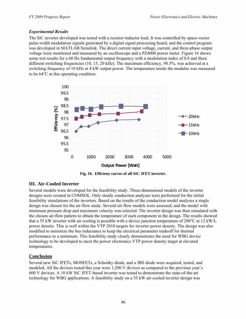
FY 2009 Progress Report Power Electronics and Electric Machines
46
Experimental Results
The SiC inverter developed was tested with a resistor-inductor load. It was controlled by space-vector pulse-width modulation signals generated by a digital signal processing board, and the control program was developed in MATLAB Simulink. The direct current input voltage, current, and three-phase output voltage were monitored and measured by an oscilloscope and a PZ4000 power meter. Figure 16 shows some test results for a 60 Hz fundamental output frequency with a modulation index of 0.8 and three different switching frequencies (10, 15, 20 kHz). The maximum efficiency, 98.5%, was achieved at a switching frequency of 10 kHz at 4 kW output power. The temperature inside the modules was measured to be 64°C at this operating condition.
9595.5
9696.5
9797.5
9898.5
9999.5100
0 1000 2000 3000 4000 5000
Output Power [Watt]
Effic
ienc
y [%
]
20kHz
15kHz
10kHz
Fig. 16. Efficieny curves of all-SiC JFET inverter.
III. Air-Cooled Inverter Several models were developed for the feasibility study. Three-dimensional models of the inverter designs were created in COMSOL. Only steady conduction analyses were performed for the initial feasibility simulations of the inverters. Based on the results of the conduction model analyses a single design was chosen for the air-flow study. Several air-flow models were assessed, and the model with minimum pressure drop and maximum velocity was selected. The inverter design was then simulated with the chosen air-flow pattern to obtain the temperature of each component in the design. The results showed that a 55 kW inverter with air cooling is possible with a device junction temperature of 200°C at 12 kW/L power density. This is well within the VTP 2010 targets for inverter power density. The design was also modified to minimize the bus inductance to keep the electrical parameter tradeoff for thermal performance to a minimum. This feasibility study clearly demonstrates the need for WBG device technology to be developed to meet the power electronics VTP power density target at elevated temperatures.
Conclusion Several new SiC JFETs, MOSFETs, a Schottky diode, and a JBS diode were acquired, tested, and modeled. All the devices tested this year were 1,200 V devices as compared to the previous year’s 600 V devices. A 10 kW SiC JFET-based inverter was tested to demonstrate the state-of-the-art technology for WBG applications. A feasibility study on a 55 kW air-cooled inverter design was

Power Electronics and Electric Machines FY 2009 Progress Report
47
completed, and results showed that air cooling is possible with a device junction temperature of 200°C, achieving a power density of 12 kW/L. Publications 1. M. Chinthavali, H. Zhang, L. M. Tolbert, and B. Ozpineci, “Update on SiC-based Inverter
Technology,” Brazilian Power Electronics Conference, September 2009 (in press).
2. M. Chinthavali, P. Otaduy, and B. Ozpineci, “Performance Comparison Study of SiC and Si Technology for an IPM-based Drive System,” International Conference on Silicon Carbide and Related Materials, October 2009 (in press).

FY 2009 Progress Report Power Electronics and Electric Machines
48
4.2 An Active Filter Approach to the Reduction of the DC Link Capacitor
Principal Investigator: Burak Ozpineci Oak Ridge National Laboratory National Transportation Research Center 2360 Cherahala Boulevard Knoxville, TN 37932 Voice: 865-946-1329; Fax: 865-946-1262; E-mail:[email protected] DOE Technology Development Manager: Susan A. Rogers Voice: 202-586-8997; Fax: 202-586-1600; E-mail: [email protected] ORNL Program Manager: Mitch Olszewski Voice: 865-946-1350; Fax: 865-946-1262; E-mail: [email protected] Objectives • To replace the bulky direct current (dc) link capacitor with a much smaller size active filter that
imitates what a dc link capacitor does. — Weight and volume of the traction inverter can be reduced while the reliability and lifetime of the
inverter will be increased. Approach • Establish performance requirements for an active filter. • Simulate an active filter that can replace a dc link capacitor for a traction inverter. Major Accomplishments • Built a simulation model of a traction drive system to establish the performance requirements for an
active power filter (APF). • Achieved an active filter approach to replace the dc link capacitor. • Analyzed the parameter dependence of the APF and the underlying barriers of this method. Future Direction None: Project concluded at end of FY 2009. Technical Discussion Background
In an electric traction system composed of a battery, dc bus, three-phase inverter, and induction motor, harmonic current in the dc bus introduced by the switching behavior of the inverter is significant. Excessive harmonic current can greatly disturb the dc bus voltage and cause thermal stress on the dc bus capacitor, interference with the communication and control system, additional heat, audible noise, mechanical stress, and vibration [1]. The dc bus capacitor is used to filter the dc bus current harmonics and to reduce the dc voltage ripple. It occupies 35–40% of the whole traction inverter volume and weight and costs up to 23% of the inverter. Electric vehicle and hybrid electric vehicle manufacturers are interested in savings in the cost, weight, and volume of these capacitors. An APF could be one way to reduce the capacitor size. This project addresses

Power Electronics and Electric Machines FY 2009 Progress Report
49
these issues by presenting a method to replace the bulky capacitor with an APF in a 55 kW traction drive system and analyzing the problems and barriers in this method. Operating Principles
A typical traction drive system is shown in Fig. 1. It consists of a dc source, an APF, a three-phase inverter, and a traction motor, which in this case is an induction motor. The synthesis of a smooth sinusoidal current, with minimum harmonics, for the alternating current motor drive with a stiff dc voltage source requires a high rate of switching with different combinations of the inverter switches. The most commonly used modulation methods are sinusoidal pulse width modulation and space vector modulation. By using these modulation methods, the output current of the inverter can be modulated to a desired sinusoidal shape, but the dc side ripple current drawn from the battery can be significant. To demonstrate the waveforms of dc bus current, a specific example using a three-phase inverter feeding a squirrel cage induction motor is used. The system parameters are shown in Table 1.
dcC
Fig.1. Hybrid electric vehicle traction drive system.
Table 1. Parameters of the Traction Drive System
Parameter Value dc bus voltage 500 V dc bus capacitor 2,200 μF Three-phase inverter switching frequency (fsw) 10 kHz Three-phase inverter modulation frequency (f m) 50 Hz Output power 55 kW Number of poles in induction motor (IM) 2 Stator resistance of IM 0.19 Ω Rotor resistance of IM 0.39 Ω Magnetizing inductance of IM 4 mH Stator and rotor leakage inductance 270 μH
The dc bus current can be obtained through a MATLAB Simulink simulation using the PLECS toolbox. Figures 2 and 3 show the dc bus ripple current before filtering and the Fourier transform of this current, respectively. Without the smoothing of the dc bus capacitor, the current pulsates between −70 A and 220 A, which is the peak phase current for the motor in this simulation. From Fig. 3, we can see that the dc component is 110 A; there are high harmonic components at fsw±3×fm, 2×fsw, 2×fsw±6×fm, 3×fsw±3×fm, 4×fsw, and 4×fsw±6×fm; and there are some low harmonic components at higher frequency.
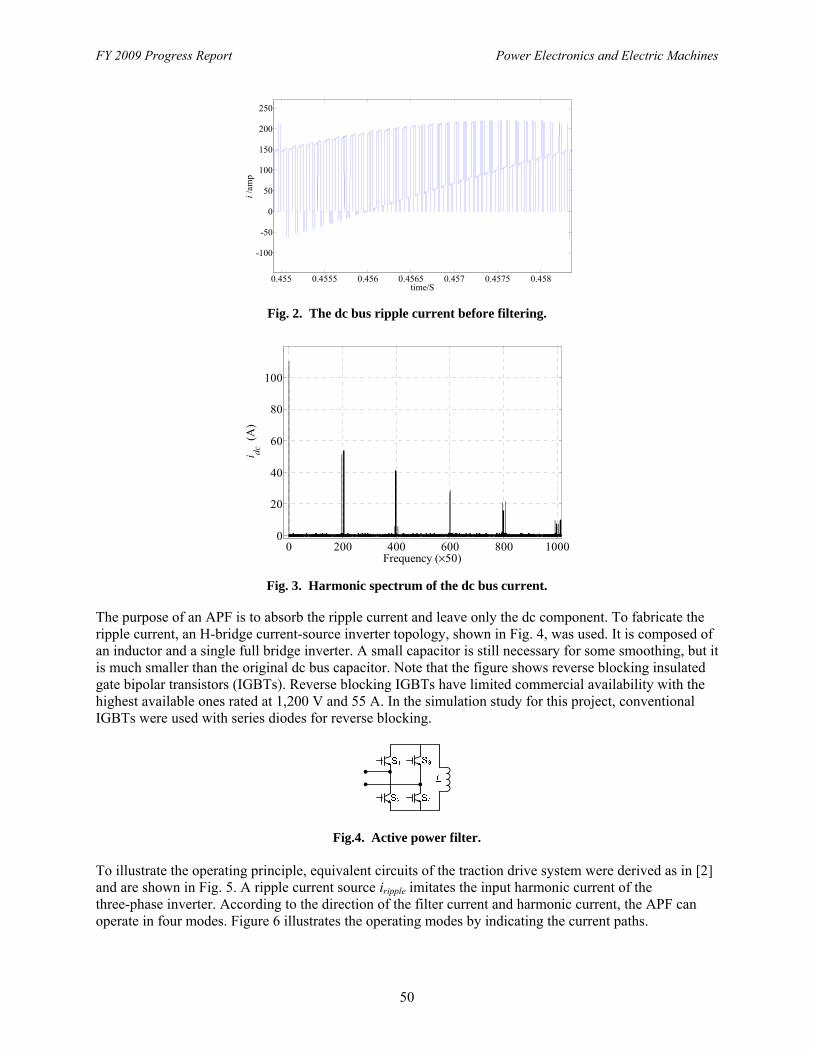
FY 2009 Progress Report Power Electronics and Electric Machines
50
Fig. 2. The dc bus ripple current before filtering.
0 200 400 600 800 10000
20
40
60
80
100
Frequency (×50)
i dc (
A)
Fig. 3. Harmonic spectrum of the dc bus current.
The purpose of an APF is to absorb the ripple current and leave only the dc component. To fabricate the ripple current, an H-bridge current-source inverter topology, shown in Fig. 4, was used. It is composed of an inductor and a single full bridge inverter. A small capacitor is still necessary for some smoothing, but it is much smaller than the original dc bus capacitor. Note that the figure shows reverse blocking insulated gate bipolar transistors (IGBTs). Reverse blocking IGBTs have limited commercial availability with the highest available ones rated at 1,200 V and 55 A. In the simulation study for this project, conventional IGBTs were used with series diodes for reverse blocking.
Fig.4. Active power filter. To illustrate the operating principle, equivalent circuits of the traction drive system were derived as in [2] and are shown in Fig. 5. A ripple current source iripple imitates the input harmonic current of the three-phase inverter. According to the direction of the filter current and harmonic current, the APF can operate in four modes. Figure 6 illustrates the operating modes by indicating the current paths.
0.455 0.4555 0.456 0.4565 0.457 0.4575 0.458
-100
-50
0
50
100
150
200
250
time/S
i /am
p

Power Electronics and Electric Machines FY 2009 Progress Report
51
rippleifLLi
dcfi
1S
2S
3S
4S
filteri
dcv Cdc
rippleifL
filteri
Li
dcfi
1S
2S
3S
4Sdcv Cdc
(a) Mode 1 (b) Mode 2 (c) Mode 3 (d) Mode 4
Fig. 5. Equivalent circuits under different operating modes.
Fig. 6. APF operating current and voltage waveforms. The operating modes are explained in detail as follows. Mode 1: When the ripple current iripple flows into the load, which is defined as positive, filter switches S1 and S4 are closed (interval between time T1 and T2 in Fig. 6) and the inductor current iL is injected into the dc bus. The direction of filter current ifilter in this mode is defined as negative. Because ifilter is larger than iripple, ifilter charges the capacitor and hence the dc bus voltage vdc increases. The following equation describes vdc:
dcdc ripple filter
dvC i i
dt= − − , (1)
where Cdc is the dc bus capacitor; dvdc and dt are the derivations of vdc and time t. Mode 2 starts once vdc reaches the upper boundary of its preset hysteresis band. Mode 2: To reduce vdc, S1 and S2 are closed; iL freewheels through them. Because the ripple current is still positive, it discharges the capacitor, and hence vdc decreases. This can be described by
.dcdc ripple
dvC i
dt= − (2)
When vdc reaches the lower bound, this mode ends. It lasts from T2 to T3 (Fig. 6). Mode 3: When the ripple current is negative, S2 and S3 are closed to produce positive ifilter; iripple goes into the filter. Because ifilter is larger than iripple, the total current discharges the capacitor, and vdc decreases as shown in interval T4 to T5 in Fig. 6. Once it reaches the lower boundary, mode 3 ends. Equation (3) describes the voltage of the dc bus during this period:
busdc ripple filter
dvC i i
dt= − − . (3)

FY 2009 Progress Report Power Electronics and Electric Machines
52
Mode 4: In this mode, S3 and S4 are closed. The inductor current iL freewheels through S3 and S4, and iripple charges the capacitor; thus, vdc increases. This mode corresponds to the time interval T5 to T6 in Fig. 6 and can be described by
.busdc ripple
dvC i
dt= − (4)
According to the operation principle depicted above, the switching strategy of an APF is influenced by two variables: dc bus voltage ripple and the ripple current generated by the three-phase inverter. The control circuit of the APF is shown in Fig. 7. Two control loops are used to generate the control signals. A dc bus voltage vdc is detected and filtered to get an average value, Vdc. Voltage ripple Δvdc is obtained by subtracting the average value Vdc from vdc, and then it is fed to a hysteresis-band controller to generate a logic signal C1. To compensate for the loss in the inductor and keep the inductor current to the desired value IL, iL is controlled by a feedback proportional-integral (PI) controller, the error eiL is taken through the PI controller, and the output is added to Δvdc. In addition, the polarity of the current ripple is detected as signal C2. A decoder is used to generate the switching signal for S1, S2, S3, and S4.
dcv
dcV
dcvΔ
LILi Li
e
dci dcID
ecod
er
Fig. 7. APF control circuit.
Simulation Results
The motor drive system with APF was modeled and simulated using MATLAB Simulink with the PLECS toolbox according to the topology and operating principles described above. The system parameters were the same as listed in the preceding section except that a 100 μF smoothing capacitor was used instead of the 2,200 μF capacitor. Four IGBTs, two diodes, and a 5 mH inductor were used for the APF. For comparison purposes, only the case with the large capacitor filter was studied. Figure 8 shows the simulation results. The left column shows current and voltage waveforms in the original single capacitor case with no APF, and the right column shows the results for the APF case. Figure 8(a) shows the dc bus current before and after filtering. Figure 8(b) shows the zoomed plot of the dc input current. The current ripple is between 160 A and 220 A before filtering. The fundamental frequency of dc bus current ripple is at 3 kHz, which is six times the modulation frequency because of the modulation of the three-phase inverter. In the passive method, the current ripple fluctuates from 3 A peak-to-peak (p-p), to 10 A p-p. While in APF method, the ripple current is also 10 A p-p because the control method is hysteresis control to keep the current within a bandwidth. Figure 8(c) shows the voltage ripple of dc bus. As with the current ripple in the passive method, the voltage ripple changes from 0.5 V p-p to 2 V p-p, while in the APF method it is strictly at 2 V p-p.

Power Electronics and Electric Machines FY 2009 Progress Report
53
Fig. 8. Simulation results for the large capacitor only case (figures on the left) and APF case (figures on the right).
Figure 9 shows the frequency spectrum of the dc input current through 250 kHz for both cases. An enlarged figure is posted at the top right corner of each one. It can be seen from the frequency spectrum that harmonic components are almost eliminated leaving only the dc current. For the capacitor only case, there are small harmonic components at fsw±3×fm, 2×fsw, 2×fsw±3×fm, 3×fsw±3×fm, and so on. The highest magnitude harmonics are 2 A at fsw±3×fm. For the APF case, the harmonic magnitude is much lower and spread throughout the spectrum; this is because the frequency of the ripple current is not constant in the APF method either.
Fig. 9. Harmonic spectrum of input current.

FY 2009 Progress Report Power Electronics and Electric Machines
54
Parameter Dependent Analysis and Barriers
As noted previously, the dc bus voltage ripple, which depends on the preset controller hysteresis band, can affect the dc input current ripple. Figure 10(a) shows the relationship between them. It is clear that, as the other circuit parameters and filter conditions remain the same, the current ripple increases as the voltage ripple monotonically increases. For instance, the current ripple is 10 A when the hysteresis band is 2 V, and is 25 A when the hysteresis band is 5 V. As shown in Fig. 5, it is clear that the sum of active filter current and load current charges or discharges the capacitor causing the voltage ripple in the capacitor, and the voltage change directly leads to the input current ripple. Therefore, current ripple can be controlled indirectly through the control of the voltage hysteresis band. The switching losses in power switches are proportional to the switching frequency, suggesting that the switching frequency should be lower for reducing APF losses. According to the simulations, two crucial parameters affecting the APF frequency can be identified: dc bus voltage ripple and the smoothing capacitor value. Because the APF changes modes to charge or discharge the capacitor, increasing the voltage hysteresis band or capacitance can increase the time of reaching the voltage boundary, which means the APF can work at a slower frequency. The relation between frequency and voltage ripple is shown in Fig. 10(b). Since the bus ripple voltage is also proportional to the current ripple, it cannot increase too much. A tradeoff should be made to determine the voltage ripple band. A range of 2 to 3 V is acceptable in this situation. On the other hand, the capacitance of the smoothing capacitor is inversely proportional to the switching frequency. When the capacitor is 1 per unit (i.e., 100 μF in the simulation), the maximum switching frequency is 160 kHz; when the capacitor increases to 5 per unit, the frequency can decrease to 26 kHz, as shown in Fig. 10(c). This is a more practical switching frequency for the IGBTs, and because the capacitance is one-fourth of the original value, the reduction is still significant. The parameter dependence relations can be explained by applying Coulomb’s law to the dc bus voltage: , (5) where ΔVdc is the dc bus voltage ripple, C is the capacitance, and ΔQ = i × Δt, which is the change in the capacitor charge. The change in the capacitor charge depends on ΔVdc and C. Thus, if C is kept constant, Δt, which is the charge or discharge time, is proportional to ΔVdc. Moreover, the average switching frequency is inversely proportional to the voltage ripple. On the other hand, if ΔVdc is kept constant, then, the switching frequency is inversely proportional to the capacitance C. Furthermore, the size of the APF inductor affects the filtering of the low frequency components. With a lower inductance, all the current and voltage waveforms show increasing low frequency ripple, as shown in Fig. 11. The frequency of oscillation is three times that of the inverter line frequency. This is because the inductance is too small to absorb the low frequency energy fluctuations in the dc bus. Although in theory an APF can replace or substantially reduce the capacitor size, there are several problems associated with the APF method which limit its practical application. Essentially, this APF solution modulates the input harmonic current to a much higher frequency; thus, a small capacitor is enough for further filtering. High switching frequency is among the disadvantages with this solution. It will be hard to find power devices that can work at high frequencies at these power levels. Moreover, the switching losses of the APF make up a significant portion of the losses in the inverter.
QVC dc Δ=Δ⋅

Power Electronics and Electric Machines FY 2009 Progress Report
55
2 3 4 5 6 7 810
15
20
25
30
35
40
Votage ripple (V)
Cur
rent
rip
ple
(A)
2 3 4 5 6 7 82
4
6
8
10
12
14
16 x 104
Voltage ripple (V)
Freq
uenc
y(H
z)
0 1 2 3 4 50
0.5
1
1.5
2 x 10⁵
Capacitance (per unit)
Freq
uenc
y (H
z)
(a) (b) (c)
Fig. 10. Parameter dependence: (a) = p-p current ripple vs p-p voltage ripple, (b) = switching frequency vs p-p voltage ripple, and (c) = switching frequency vs capacitance.
(a) (b) (c)
Fig. 11. Effects of filter inductance: (a) = input current, (b) = dc bus voltage, and (c) = APF inductor. Another disadvantage is the high inductor current. The inductor current is around one-half of the maximum load current; in this case, it is 110 A. Thick coil wire is necessary for high inductor current. This means additional volume and weight for the inductor and high equivalent series resistance loss. Although the inductor is much more reliable and long lasting than the capacitor, the power switches and diodes introduced in the APF method can decrease the reliability. Conclusion This project evaluates a solution for reduction of the bulky dc bus capacitor by using an APF in a three-phase traction system. Detailed operation modes are presented, and the simulation of this method is described. With this APF control method, the dc bus capacitor can be dramatically minimized, from 2,200 μF to 100 μF. However, because of the high operation frequency and the large inductor current, the size and weight of the APF, and the loss associated with the additional semiconductor switches, the APF method is still far from being practical in a traction drive inverter. Publications S. Li, B. Ozpineci, and L. M. Tolbert, “Evaluation of a Current Source Active Power Filter to Reduce the DC Bus Capacitor in a Hybrid Electric Vehicle Traction Drive,” 2009 IEEE Energy Conversion Congress and Exposition. References 1. V. Jouanne, A. Wallace, M. MillsPrice, T. Lewis, K. Rhinefrank, and E. Amon, “Hybrid electric
vehicle DC-bus traction drive harmonics,” in Proc. 2005 IEEE International Conf. on Electric Machines and Drives, pp: 235–242.

FY 2009 Progress Report Power Electronics and Electric Machines
56
2. B. K. Bose and D. Kastha, “Electrolytic capacitor elimination in power electronic system by high frequency active filter,” in Proc. 1991 IEEE Industry Applications Society Annual Meeting, pp. 869–878.
3. V. Jouanne, A. Wallace, M. MillsPrice, T. Lewis, K. Rhinefrank, and E. Amon, “Harmonic mitigation techniques for hybrid electric vehicle DC-bus traction drives,” in Proc. 2005 IEEE Conference on Vehicle Power and Propulsion, pp. 688–693.
4. G. Gu and K. Nam, “A DC link capacitor minimization method through direct capacitor current control,” in Proc. 2002 IEEE Industry Applications Society Annual Meeting, pp. 811–817.
5. W. Ping, S. Liangyu, and L. Bin, “Research of inverter with the ability to harmonic compensation,” in Proc. 2002 International Conf. on Power System Technology, pp. 2261–2264.
6. J. S. Lai, H. Kouns, and J. Bond, “A low-inductance DC bus capacitor for high power traction motor drive inverters,” in Proc. 2002 IEEE Industry Applications Society Annual Meeting, pp. 955–962.
7. B. Singh, K. Al-Haddad, and A. Chandra, “A review of active filters for power quality improvement,” IEEE Transactions on Industrial Electronics, Vol. 46, 1999, pp. 960–972.
8. F. Z. Peng, “Harmonic sources and filtering approaches,” IEEE Industry Applications Magazine, Vol. 7, 2001, pp. 18–25.
9. L. Malesani, L. Rossetto, and P. Tenti, “Active power filter with hybrid energy storage,” IEEE Transactions on Power Electronics, Vol. 6, 1991, pp. 392–397.
10. T. Shimizu, Y. Jin, and G. Kimura, “DC ripple current reduction on a single-phase PWM voltage-source rectifier,” IEEE Transactions on Industry Applications, Vol. 36, 2000, pp.1419–1428.
11. R. Wang, F. Wang, R. Lai, P. Ning, R. Burgos, and D. Boroyevich, “Study of energy storage capacitor reduction for single phase PWM rectifier,” 2009 IEEE Applied Power Electronics Conference and Exposition, pp. 1177–1183.
Patents None.

Power Electronics and Electric Machines FY 2009 Progress Report
57
4.3 High Temperature, High Voltage Fully Integrated Gate Driver Circuit
Principal Investigator: Leon M. Tolbert Oak Ridge National Laboratory National Transportation Research Center 2360 Cherahala Boulevard Knoxville, TN 37932 Voice: 865-946-1332; Fax: 865-946-1262; E-mail: [email protected] DOE Technology Development Manager: Susan A. Rogers Voice: 202-586-8997; Fax: 202-586-1600; E-mail: [email protected] ORNL Program Manager: Mitch Olszewski Voice: 865-946-1350; Fax: 865-946-1262; E-mail: [email protected] Objectives • Increase the current drive of the high temperature gate driver circuit. • Improve the gate driver design to make it more robust against temperature variation. • Incorporate three protective features with the core gate driver circuit: undervoltage protection, short
circuit protection (SCP), and thermal shutdown. • Insert multiple on-chip voltage regulators in the same die. Approach • Make use of the bipolar complementary metal-oxide semiconductor (CMOS)–double diffused
metal-oxide semiconductor (DMOS) on silicon-on-insulator (SOI) process features to optimize the gate driver design for high ambient temperature operation.
• Test different types of wide bandgap semiconductor power switches with the driver circuit. Major Accomplishments • Designed and taped out the third generation (3G) gate driver circuit, which has current drive strength
of more than 5 A at room temperature. • Optimized design by making some of the critical functional blocks in the 3G gate driver circuit
temperature-insensitive. • Incorporated multiple voltage regulator circuits in the gate driver chip. • Integrated SCP, undervoltage lockout (UVLO), and thermal shutdown circuitries with the core gate
driver circuit. Future Direction • Results of 2009 chip research will be used to identify circuit blocks requiring design improvements,
and design modifications. • The circuit topology and layout will be enhanced to decrease the area of the gate driver chip and
enhance robustness over a wide temperature range. • Desaturation methods will be explored for SCP design. • Power switch gate current monitoring circuitry will be added in the fourth generation gate driver chip.
Technical Discussion The goal of this project is to develop an SOI-based high temperature, high voltage gate driver integrated circuit with high drive current capability for wide bandgap (WBG) power switches. Power electronics in
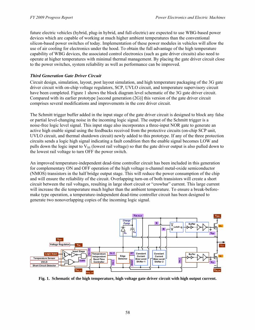
FY 2009 Progress Report Power Electronics and Electric Machines
58
future electric vehicles (hybrid, plug-in hybrid, and full-electric) are expected to use WBG-based power devices which are capable of working at much higher ambient temperatures than the conventional silicon-based power switches of today. Implementation of these power modules in vehicles will allow the use of air cooling for electronics under the hood. To obtain the full advantage of the high temperature capability of WBG devices, the associated control electronics (such as gate driver circuits) also need to operate at higher temperatures with minimal thermal management. By placing the gate driver circuit close to the power switches, system reliability as well as performance can be improved. Third Generation Gate Driver Circuit
Circuit design, simulation, layout, post layout simulation, and high temperature packaging of the 3G gate driver circuit with on-chip voltage regulators, SCP, UVLO circuit, and temperature supervisory circuit have been completed. Figure 1 shows the block diagram level schematic of the 3G gate driver circuit. Compared with its earlier prototype [second generation (2G)] this version of the gate driver circuit comprises several modifications and improvements in the core driver circuit. The Schmitt trigger buffer added in the input stage of the gate driver circuit is designed to block any false or partial level-changing noise in the incoming logic signal. The output of the Schmitt trigger is a noise-free logic level signal. This input stage also incorporates a three-input NOR gate to generate an active high enable signal using the feedbacks received from the protective circuits (on-chip SCP unit, UVLO circuit, and thermal shutdown circuit) newly added to this prototype. If any of the three protection circuits sends a logic high signal indicating a fault condition then the enable signal becomes LOW and pulls down the logic input to VSS (lowest rail voltage) so that the gate driver output is also pulled down to the lowest rail voltage to turn OFF the power switch. An improved temperature-independent dead-time controller circuit has been included in this generation for complementary ON and OFF operation of the high voltage n-channel metal-oxide semiconductor (NMOS) transistors in the half bridge output stage. This will reduce the power consumption of the chip and will ensure the reliability of the circuit. Overlapping turn-on of both transistors will create a short circuit between the rail voltages, resulting in large short circuit or “crowbar” current. This large current will increase the die temperature much higher than the ambient temperature. To ensure a break-before-make type operation, a temperature-independent dead-time controller circuit has been designed to generate two nonoverlapping copies of the incoming logic signal.
Fig. 1. Schematic of the high temperature, high voltage gate driver circuit with high output current.

Power Electronics and Electric Machines FY 2009 Progress Report
59
Fig. 2. Temperature-independent dead-time controller circuit.
Fig. 4. Schematic of the temperature-independent
adjustable delay controller circuit.
Fig. 3. Schematic of the
temperature-independent current bias network.
Figure 5. Schematic of the
temperature-independent level shifter circuit.
Figure 2 shows the schematic of the proposed dead-time controller circuit. The main building block of this dead-time controller circuit is the adjustable delay controller circuit that can inject a temperature-independent phase lag to an incoming logic signal. A temperature-independent current bias circuit has been designed to provide constant current biasing to the adjustable delay controller circuit. Figure 3 shows the schematic of the temperature-independent current bias network developed using the zero-temperature coefficient (ZTC) [1] bias conditions of the NMOS and the p-channel metal-oxide semiconductor (PMOS) transistors. Figure 4 shows the schematic of the adjustable delay controller circuit with the temperature-independent bias network. Constant bias voltage is supplied to the gates of all the PMOS transistors, which source constant pull-up currents to the inverters, and thus capacitors get charged by a constant current across the entire temperature range. Similarly, the constant bias voltage is provided to all the NMOS transistors, which sink the constant pull down current from the
inverters. This ensures the same rate of discharge of the capacitors over temperatures. Because the capacitors get charged and discharged by constant currents for the entire temperature range, the phase shift injected by this circuit remains virtually constant over the temperature range.
A constant current biased level shifter circuit has been designed for this version of the gate driver circuit. The main philosophy of the level shifter circuit is to convert the logic level voltage (SET and RESET) into currents and then, on the high voltage side, convert this current back into a voltage referenced to the high-side voltage. Constant current bias is guaranteed through the ZTC biasing of the PMOS and the NMOS current mirrors in the level shifter circuit as shown in Fig. 5. The high-side (MH) buffer (see Fig. 1) used to drive the MH high voltage NMOS (HVNMOS) transistor has been redesigned using only low voltage devices (5 V PMOSs and NMOSs). In the previous design 45 V devices were used for this buffer to keep all the devices within the safe operating area. Because of this modification, the same buffer structure can be used for
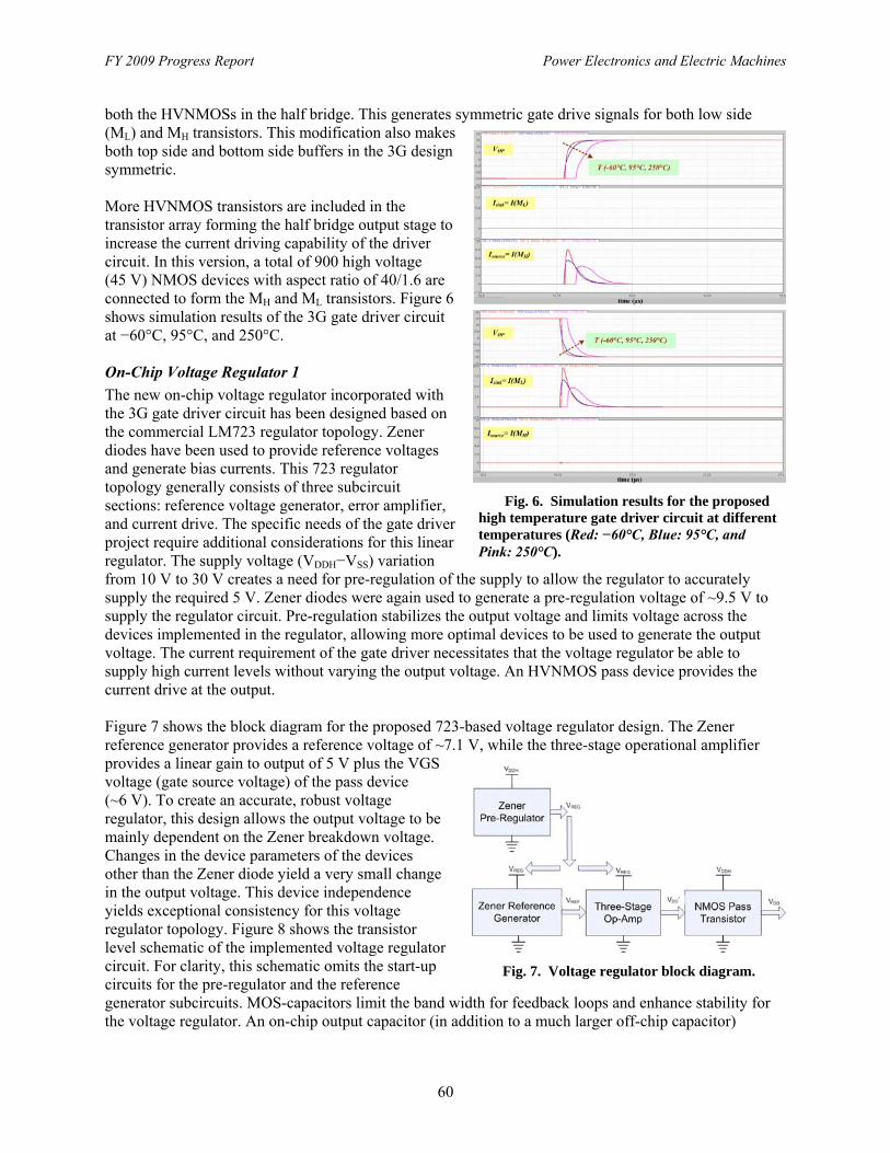
FY 2009 Progress Report Power Electronics and Electric Machines
60
Fig. 7. Voltage regulator block diagram.
Fig. 6. Simulation results for the proposed high temperature gate driver circuit at different temperatures (Red: −60°C, Blue: 95°C, and Pink: 250°C).
both the HVNMOSs in the half bridge. This generates symmetric gate drive signals for both low side (ML) and MH transistors. This modification also makes both top side and bottom side buffers in the 3G design symmetric. More HVNMOS transistors are included in the transistor array forming the half bridge output stage to increase the current driving capability of the driver circuit. In this version, a total of 900 high voltage (45 V) NMOS devices with aspect ratio of 40/1.6 are connected to form the MH and ML transistors. Figure 6 shows simulation results of the 3G gate driver circuit at −60°C, 95°C, and 250°C.
On-Chip Voltage Regulator 1
The new on-chip voltage regulator incorporated with the 3G gate driver circuit has been designed based on the commercial LM723 regulator topology. Zener diodes have been used to provide reference voltages and generate bias currents. This 723 regulator topology generally consists of three subcircuit sections: reference voltage generator, error amplifier, and current drive. The specific needs of the gate driver project require additional considerations for this linear regulator. The supply voltage (VDDH−VSS) variation from 10 V to 30 V creates a need for pre-regulation of the supply to allow the regulator to accurately supply the required 5 V. Zener diodes were again used to generate a pre-regulation voltage of ~9.5 V to supply the regulator circuit. Pre-regulation stabilizes the output voltage and limits voltage across the devices implemented in the regulator, allowing more optimal devices to be used to generate the output voltage. The current requirement of the gate driver necessitates that the voltage regulator be able to supply high current levels without varying the output voltage. An HVNMOS pass device provides the current drive at the output. Figure 7 shows the block diagram for the proposed 723-based voltage regulator design. The Zener reference generator provides a reference voltage of ~7.1 V, while the three-stage operational amplifier provides a linear gain to output of 5 V plus the VGS voltage (gate source voltage) of the pass device (~6 V). To create an accurate, robust voltage regulator, this design allows the output voltage to be mainly dependent on the Zener breakdown voltage. Changes in the device parameters of the devices other than the Zener diode yield a very small change in the output voltage. This device independence yields exceptional consistency for this voltage regulator topology. Figure 8 shows the transistor level schematic of the implemented voltage regulator circuit. For clarity, this schematic omits the start-up circuits for the pre-regulator and the reference generator subcircuits. MOS-capacitors limit the band width for feedback loops and enhance stability for the voltage regulator. An on-chip output capacitor (in addition to a much larger off-chip capacitor)
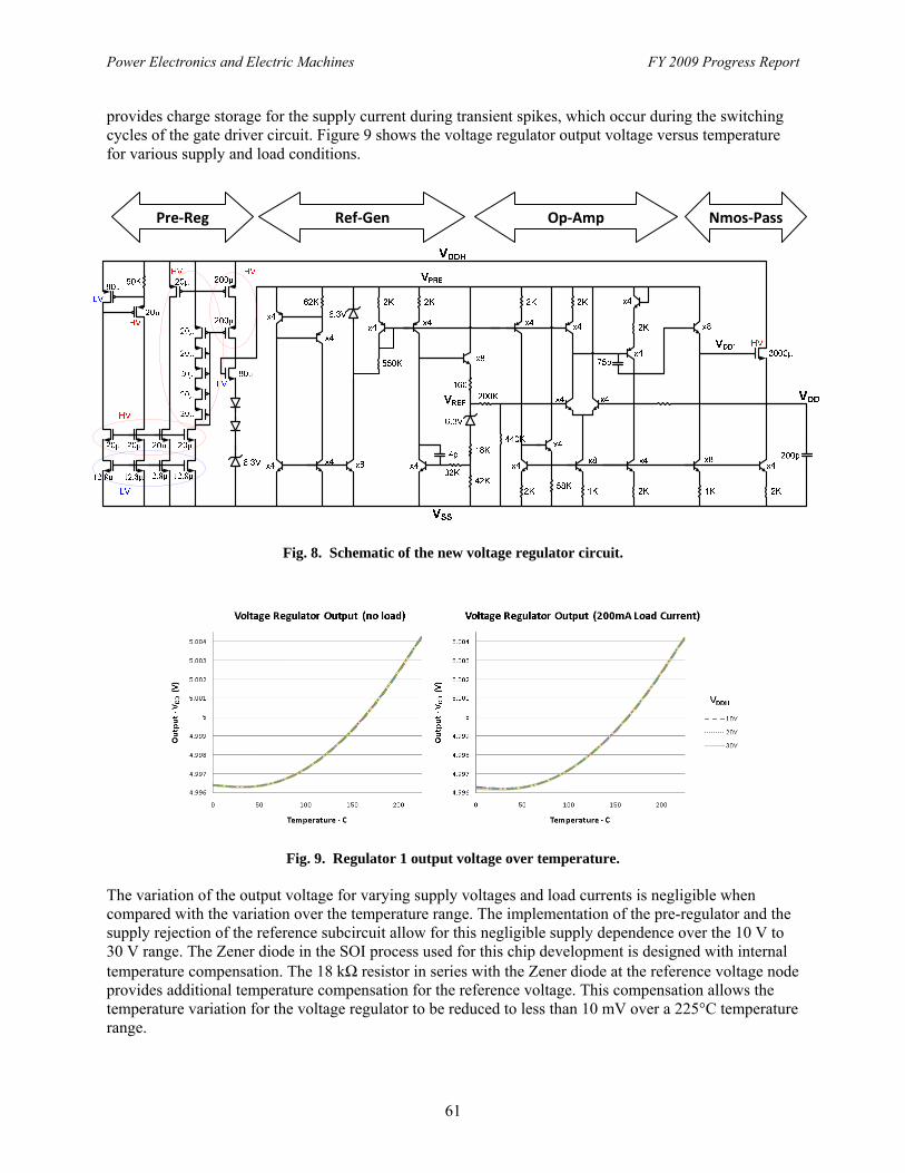
Power Electronics and Electric Machines FY 2009 Progress Report
61
provides charge storage for the supply current during transient spikes, which occur during the switching cycles of the gate driver circuit. Figure 9 shows the voltage regulator output voltage versus temperature for various supply and load conditions.
Fig. 8. Schematic of the new voltage regulator circuit.
Fig. 9. Regulator 1 output voltage over temperature. The variation of the output voltage for varying supply voltages and load currents is negligible when compared with the variation over the temperature range. The implementation of the pre-regulator and the supply rejection of the reference subcircuit allow for this negligible supply dependence over the 10 V to 30 V range. The Zener diode in the SOI process used for this chip development is designed with internal temperature compensation. The 18 kΩ resistor in series with the Zener diode at the reference voltage node provides additional temperature compensation for the reference voltage. This compensation allows the temperature variation for the voltage regulator to be reduced to less than 10 mV over a 225°C temperature range.
Pre-Reg Ref-Gen Op-Amp Nmos-Pass

FY 2009 Progress Report Power Electronics and Electric Machines
62
Fig. 11. Schematic of the high voltage, high temperature linear voltage regulator circuit.
Fig. 10. Monte Carlo analysis for process and mismatch variation.
Figure 10 shows the Monte Carlo statistical results for 100 runs of process and mismatch variation. The nature of the 723 voltage-regulator design allows the output voltage to be nearly independent of all devices (except the Zener diode). Drastic changes in the parameters of the bipolar junction transistor and metal-oxide semiconductor field-effect transistor (MOSFET) devices as well the passive components yield negligible changes in the output of the regulator. Independence on the passive components (specifically resistors) is critical for accurate, consistent regulator performance due to the inherent inconsistency of the on-chip resistors. As a result of this robust design, the regulator will yield consistent results from chip to chip. In addition to robustness against fabrication related process variations and device mismatches, this regulator design will yield consistent results even with poor device models. (See Table 1 for a summary of the preceding.)
Table 1. Summary of Voltage Regulator Specifications
Nominal output voltage 5 V
Output current range 0–250 mA (∆VDD < 70 µV)
Supply voltage range (VDDH–VSS) 8.4 V–45 V
Temperature variation 36 µV/°C
Line regulation 2 µV/V @ 200°C
Process and mismatch variation (100 runs) ~40 mV
On-Chip Voltage Regulator 2
The on-chip voltage regulator circuit which was first incorporated in the 2G gate driver circuit has been redesigned to increase its current drive strength. Figure 11 is a schematic of this modified high voltage, high temperature linear voltage regulator circuit. This step-down voltage regulator is needed to convert the unregulated high input dc voltage (VDDH) to a regulated nominal CMOS voltage (VDD). This step-down voltage regulator will supply voltage to the low-side buffer and other digital and analog circuits inside the gate driver circuit.
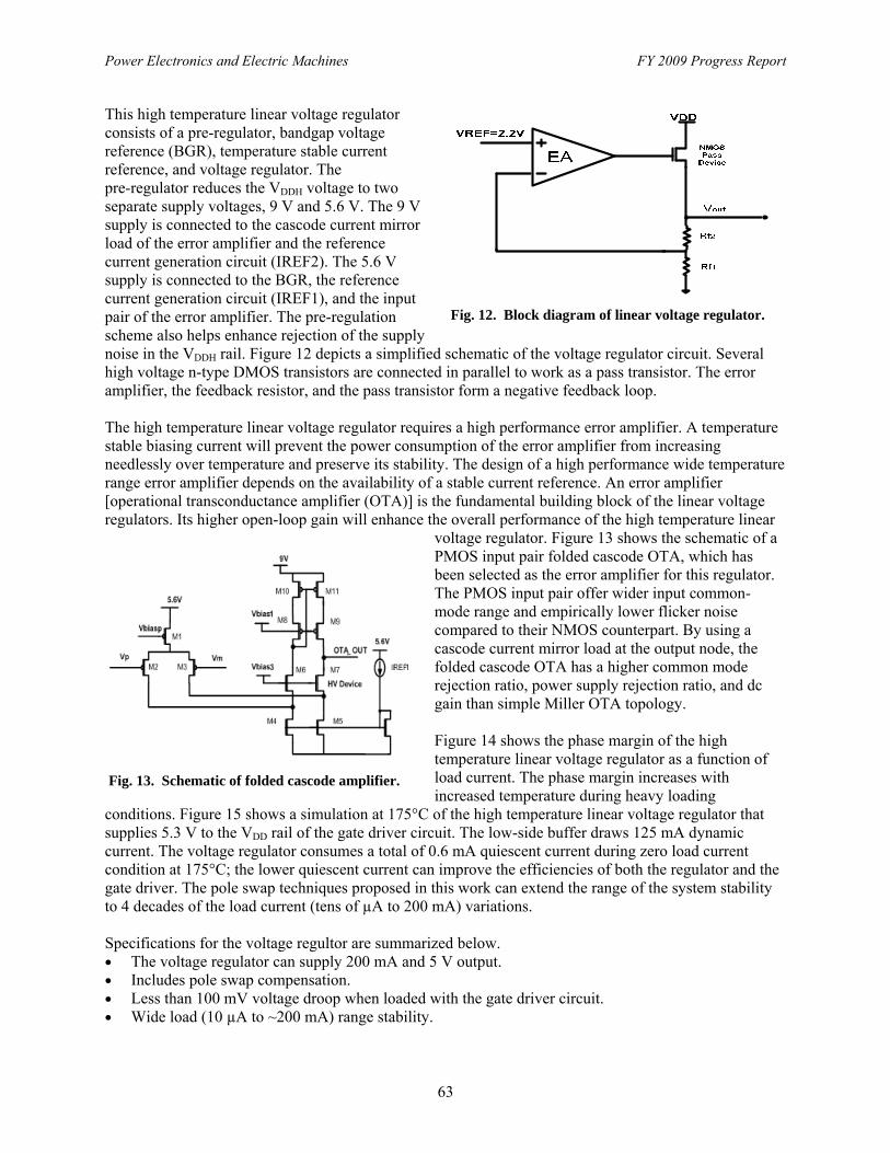
Power Electronics and Electric Machines FY 2009 Progress Report
63
Fig. 13. Schematic of folded cascode amplifier.
Fig. 12. Block diagram of linear voltage regulator.
This high temperature linear voltage regulator consists of a pre-regulator, bandgap voltage reference (BGR), temperature stable current reference, and voltage regulator. The pre-regulator reduces the VDDH voltage to two separate supply voltages, 9 V and 5.6 V. The 9 V supply is connected to the cascode current mirror load of the error amplifier and the reference current generation circuit (IREF2). The 5.6 V supply is connected to the BGR, the reference current generation circuit (IREF1), and the input pair of the error amplifier. The pre-regulation scheme also helps enhance rejection of the supply noise in the VDDH rail. Figure 12 depicts a simplified schematic of the voltage regulator circuit. Several high voltage n-type DMOS transistors are connected in parallel to work as a pass transistor. The error amplifier, the feedback resistor, and the pass transistor form a negative feedback loop. The high temperature linear voltage regulator requires a high performance error amplifier. A temperature stable biasing current will prevent the power consumption of the error amplifier from increasing needlessly over temperature and preserve its stability. The design of a high performance wide temperature range error amplifier depends on the availability of a stable current reference. An error amplifier [operational transconductance amplifier (OTA)] is the fundamental building block of the linear voltage regulators. Its higher open-loop gain will enhance the overall performance of the high temperature linear
voltage regulator. Figure 13 shows the schematic of a PMOS input pair folded cascode OTA, which has been selected as the error amplifier for this regulator. The PMOS input pair offer wider input common-mode range and empirically lower flicker noise compared to their NMOS counterpart. By using a cascode current mirror load at the output node, the folded cascode OTA has a higher common mode rejection ratio, power supply rejection ratio, and dc gain than simple Miller OTA topology. Figure 14 shows the phase margin of the high temperature linear voltage regulator as a function of load current. The phase margin increases with increased temperature during heavy loading
conditions. Figure 15 shows a simulation at 175°C of the high temperature linear voltage regulator that supplies 5.3 V to the VDD rail of the gate driver circuit. The low-side buffer draws 125 mA dynamic current. The voltage regulator consumes a total of 0.6 mA quiescent current during zero load current condition at 175°C; the lower quiescent current can improve the efficiencies of both the regulator and the gate driver. The pole swap techniques proposed in this work can extend the range of the system stability to 4 decades of the load current (tens of µA to 200 mA) variations. Specifications for the voltage regultor are summarized below. • The voltage regulator can supply 200 mA and 5 V output. • Includes pole swap compensation. • Less than 100 mV voltage droop when loaded with the gate driver circuit. • Wide load (10 µA to ~200 mA) range stability.
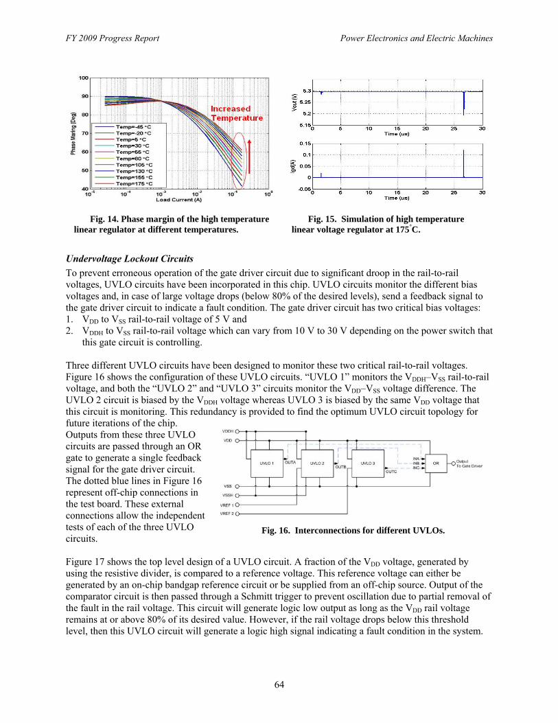
FY 2009 Progress Report Power Electronics and Electric Machines
64
Fig. 16. Interconnections for different UVLOs.
Fig. 14. Phase margin of the high temperature linear regulator at different temperatures.
Fig. 15. Simulation of high temperature linear voltage regulator at 175°C.
Undervoltage Lockout Circuits
To prevent erroneous operation of the gate driver circuit due to significant droop in the rail-to-rail voltages, UVLO circuits have been incorporated in this chip. UVLO circuits monitor the different bias voltages and, in case of large voltage drops (below 80% of the desired levels), send a feedback signal to the gate driver circuit to indicate a fault condition. The gate driver circuit has two critical bias voltages: 1. VDD to VSS rail-to-rail voltage of 5 V and 2. VDDH to VSS rail-to-rail voltage which can vary from 10 V to 30 V depending on the power switch that
this gate circuit is controlling. Three different UVLO circuits have been designed to monitor these two critical rail-to-rail voltages. Figure 16 shows the configuration of these UVLO circuits. “UVLO 1” monitors the VDDH–VSS rail-to-rail voltage, and both the “UVLO 2” and “UVLO 3” circuits monitor the VDD–VSS voltage difference. The UVLO 2 circuit is biased by the VDDH voltage whereas UVLO 3 is biased by the same VDD voltage that this circuit is monitoring. This redundancy is provided to find the optimum UVLO circuit topology for future iterations of the chip. Outputs from these three UVLO circuits are passed through an OR gate to generate a single feedback signal for the gate driver circuit. The dotted blue lines in Figure 16 represent off-chip connections in the test board. These external connections allow the independent tests of each of the three UVLO circuits. Figure 17 shows the top level design of a UVLO circuit. A fraction of the VDD voltage, generated by using the resistive divider, is compared to a reference voltage. This reference voltage can either be generated by an on-chip bandgap reference circuit or be supplied from an off-chip source. Output of the comparator circuit is then passed through a Schmitt trigger to prevent oscillation due to partial removal of the fault in the rail voltage. This circuit will generate logic low output as long as the VDD rail voltage remains at or above 80% of its desired value. However, if the rail voltage drops below this threshold level, then this UVLO circuit will generate a logic high signal indicating a fault condition in the system.
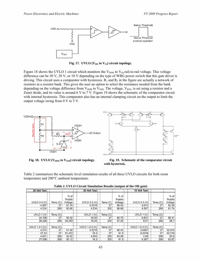
Power Electronics and Electric Machines FY 2009 Progress Report
65
Fig. 17. UVLO (VDD to VSS) circuit topology.
Figure 18 shows the UVLO 1 circuit which monitors the VDDH to VSS rail-to-rail voltage. This voltage difference can be 30 V, 20 V, or 10 V depending on the type of WBG power switch that this gate driver is driving. This circuit uses a comparator with hysteresis. R1 and R2 in the figure are actually a network of resistors in a resistor bank. This gives the user an option to select the resistance needed from the bank depending on the voltage difference from VDDH to VSSH. The voltage, VREF, is set using a resistor and a Zener diode, and its value is around 6 V to 7 V. Figure 19 shows the schematic of the comparator circuit with internal hysteresis. This comparator also has an internal clamping circuit on the output to limit the output voltage swing from 0 V to 5 V.
Fig. 18. UVLO (VDDH to VSSH) circuit topology. Fig. 19. Schematic of the comparator circuit with hysteresis.
Table 2 summarizes the schematic level simulation results of all three UVLO circuits for both room temperature and 200°C ambient temperature.
Table 2. UVLO Circuit Simulation Results (output of the OR gate)
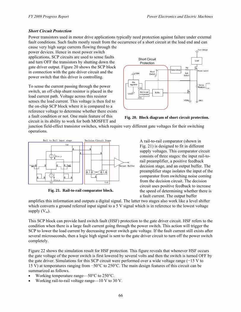
FY 2009 Progress Report Power Electronics and Electric Machines
66
Fig. 21. Rail-to-rail comparator block.
Fig. 20. Block diagram of short circuit protection.
Short Circuit Protection
Power transistors used in motor drive applications typically need protection against failure under external fault conditions. Such faults mostly result from the occurrence of a short circuit at the load end and can cause very high surge currents flowing through the power devices. Hence in most power switch applications, SCP circuits are used to sense faults and turn OFF the transistors by shutting down the gate driver output. Figure 20 shows the SCP block in connection with the gate driver circuit and the power switch that this driver is controlling.
To sense the current passing through the power switch, an off-chip shunt resistor is placed in the load current path. Voltage across this resistor senses the load current. This voltage is then fed to the on-chip SCP block where it is compared to a reference voltage to determine whether there exists a fault condition or not. One main feature of this circuit is its ability to work for both MOSFET and junction field-effect transistor switches, which require very different gate voltages for their switching operations.
A rail-to-rail comparator (shown in Fig. 21) is designed to fit in different supply voltages. This comparator circuit consists of three stages: the input rail-to-rail preamplifier, a positive feedback decision stage, and an output buffer. The preamplifier stage isolates the input of the comparator from switching noise coming from the decision circuit. The decision circuit uses positive feedback to increase the speed of determining whether there is a fault current. The output buffer
amplifies this information and outputs a digital signal. The latter two stages also work like a level shifter which converts a ground referred input signal to a 5 V signal which is in reference to the lowest voltage supply (Vss). This SCP block can provide hard switch fault (HSF) protection to the gate driver circuit. HSF refers to the condition when there is a large fault current going through the power switch. This action will trigger the SCP to lower the load current by decreasing power switch gate voltage. If the fault current still exists after several microseconds, then a logic high signal is sent to the gate driver circuit to turn off the power switch completely. Figure 22 shows the simulation result for HSF protection. This figure reveals that whenever HSF occurs the gate voltage of the power switch is first lowered by several volts and then the switch is turned OFF by the gate driver. Simulations for this SCP circuit were performed over a wide voltage range (−15 V to 15 V) at temperatures ranging from −50°C to 250°C. The main design features of this circuit can be summarized as follows. • Working temperature range—50°C to 250°C. • Working rail-to-rail voltage range—10 V to 30 V.
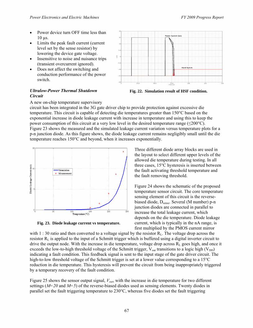
Power Electronics and Electric Machines FY 2009 Progress Report
67
Fig. 22. Simulation result of HSF condition.
• Power device turn OFF time less than 10 µs.
• Limits the peak fault current (current level set by the sense resistor) by lowering the device gate voltage.
• Insensitive to noise and nuisance trips (transient overcurrent ignored).
• Does not affect the switching and conduction performance of the power switch.
Ultralow-Power Thermal Shutdown Circuit
A new on-chip temperature supervisory circuit has been integrated in the 3G gate driver chip to provide protection against excessive die temperature. This circuit is capable of detecting die temperatures greater than 150°C based on the exponential increase in diode leakage current with increase in temperature and using this to keep the power consumption of this circuit at a very low level in the desired temperature range (≤200°C). Figure 23 shows the measured and the simulated leakage current variation versus temperature plots for a p-n junction diode. As this figure shows, the diode leakage current remains negligibly small until the die temperature reaches 150°C and beyond, when it increases exponentially.
Three different diode array blocks are used in the layout to select different upper levels of the allowed die temperature during testing. In all three cases, 15°C hysteresis is inserted between the fault activating threshold temperature and the fault removing threshold. Figure 24 shows the schematic of the proposed temperature sensor circuit. The core temperature sensing element of this circuit is the reverse-biased diode, Dsense. Several (M number) p-n junction diodes are connected in parallel to increase the total leakage current, which depends on the die temperature. Diode leakage current, which is typically in the nA range, is first multiplied by the PMOS current mirror
with 1 : 30 ratio and then converted to a voltage signal by the resistor RL. The voltage drop across the resistor RL is applied to the input of a Schmitt trigger which is buffered using a digital inverter circuit to drive the output node. With the increase in die temperature, voltage drop across RL goes high, and once it exceeds the low-to-high threshold voltage of the Schmitt trigger, Vout transitions to a logic high (VDD) indicating a fault condition. This feedback signal is sent to the input stage of the gate driver circuit. The high-to-low threshold voltage of the Schmitt trigger is set at a lower value corresponding to a 15°C reduction in die temperature. This hysteresis will prevent the circuit from being inappropriately triggered by a temporary recovery of the fault condition. Figure 25 shows the sensor output signal, Vout, with the increase in die temperature for two different settings (M=20 and M=5) of the reverse-biased diodes used as sensing elements. Twenty diodes in parallel set the fault triggering temperature to 230°C, whereas five diodes set the fault triggering
Fig. 23. Diode leakage current vs temperature.
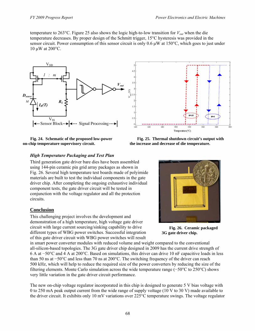
FY 2009 Progress Report Power Electronics and Electric Machines
68
Fig. 26. Ceramic packaged
3G gate driver chip.
temperature to 263°C. Figure 25 also shows the logic high-to-low transition for Vout when the die temperature decreases. By proper design of the Schmitt trigger, 15°C hysteresis was provided in the sensor circuit. Power consumption of this sensor circuit is only 0.6 μW at 150°C, which goes to just under 10 μW at 200°C.
High Temperature Packaging and Test Plan
Third generation gate driver bare dies have been assembled using 144-pin ceramic pin grid array packages as shown in Fig. 26. Several high temperature test boards made of polyimide materials are built to test the individual components in the gate driver chip. After completing the ongoing exhaustive individual component tests, the gate driver circuit will be tested in conjunction with the voltage regulator and all the protection circuits. Conclusion This challenging project involves the development and demonstration of a high temperature, high voltage gate driver circuit with large current sourcing/sinking capability to drive different types of WBG power switches. Successful integration of this gate driver circuit with WBG power switches will result in smart power converter modules with reduced volume and weight compared to the conventional all-silicon-based topologies. The 3G gate driver chip designed in 2009 has the current drive strength of 6 A at −50°C and 4 A at 200°C. Based on simulations, this driver can drive 10 nF capacitive loads in less than 50 ns at −50°C and less than 70 ns at 200°C. The switching frequency of the driver can reach 500 kHz, which will help to reduce the required size of the power converters by reducing the size of the filtering elements. Monte Carlo simulation across the wide temperature range (−50°C to 250°C) shows very little variation in the gate driver circuit performance. The new on-chip voltage regulator incorporated in this chip is designed to generate 5 V bias voltage with 0 to 250 mA peak output current from the wide range of supply voltage (10 V to 30 V) made available to the driver circuit. It exhibits only 10 mV variations over 225°C temperature swings. The voltage regulator
Fig. 24. Schematic of the proposed low-power on-chip temperature supervisory circuit.
Fig. 25. Thermal shutdown circuit’s output with the increase and decrease of die temperature.

Power Electronics and Electric Machines FY 2009 Progress Report
69
design, which was first incorporated in the previous (2G) gate driver chip, has been redesigned to increase its current capability to 200 mA. Voltage droop for this second regulator circuit is less than 100 mV, and it exhibits good stability for a wide range of load currents (10 µA to 200 mA). The SCP monitors the load current through the power switch that this gate driver chip is controlling. The UVLO circuits protect the gate driver from erroneous operation due to droop (below 80% of nominal) in the rail-to-rail voltages. The thermal shutdown circuit, which is designed to protect the chip from excessive die temperature (≥220°C), consumes less than 10 µW up to 200°C. In case of any fault, detected by one of these three protective circuits, a feedback signal is send to the gate driver circuit. In response to this fault detection, the gate driver circuit turns OFF the power switch to prevent system failure.
Publications 1. M. A. Huque, L. M. Tolbert, B. Blalock, and S. K. Islam, “SOI-based high-voltage, high-temperature
integrated circuit gate driver for SiC-based power FETs,” IET Proceedings on Power Electronics, Vol. 3, 2010, (in press).
2. M. A. Huque, L. M. Tolbert, B. J. Blalock, and S. K. Islam, A High-Temperature, High-Voltage SOI Gate Driver IC with High Output Current and On-Chip Low-Power Temperature Sensor, accepted for publication in 42nd International Symposium on Microelectronics (IMAPS 2009), San Jose, California, November 1–5, 2009.
3. M. A. Huque, S. K. Islam, B. J. Blalock, and L. M. Tolbert, “Diode leakage current based low power, on-chip high temperature sensor circuit,” in Proc. of 18th Annual Symposium on Micro- and Nano-technologies for Electronics, Photonics, Biosensors, and Alternate Energy Sources (CMOC 2009), Yale University, New Haven, Connecticut, March 11, 2009, pp. 57–58.
4. M. A Huque, S. K. Islam, B. J. Blalock, C. Su, R. Vijayaraghavan, and L M. Tolbert, “Silicon-on-insulator based high-temperature electronics for automotive applications,” in Proc. of IEEE International Symposium on Industrial Electronics (ISIE 2008), Cambridge, UK, June 30–July 2, 2008, pp. 2538–2543.
5. M. A Huque, B. J. Blalock, C. Su, R. Vijayaraghavan, S. K. Islam, and L. M. Tolbert, “SOI based integrated circuits for high-temperature applications,” in Proc. of International Conference and Exhibition on High Temperature Electronics (HiTEC 2008), Albuquerque, New Mexico, May 13–15, 2008.
References 1. F. S. Shoucair, “Analytical and experimental methods for zero-temperature-coefficient biasing of
MOS transistors,” Electronics Letters, Vol. 25(17), 1989, pp. 1196–1198. Patents None

FY 2009 Progress Report Power Electronics and Electric Machines
70
4.4 Current Source Inverter
Principal Investigator: Gui-Jia Su Oak Ridge National Laboratory National Transportation Research Center 2360 Cherahala Boulevard Knoxville, TN 37932 Voice: 865-946-1330; Fax: 865-946-1262; E-mail: [email protected] DOE Technology Development Manager: Susan A. Rogers Voice: 202-586-8997; Fax: 202-586-1600; E-mail: [email protected] ORNL Program Manager: Mitch Olszewski Voice: 865-946-1350; Fax: 865-946-1262; E-mail: [email protected] Objectives • Overall project objectives
⎯ Eliminate the drawbacks of the voltage source inverter (VSI) by switching to a current-source–based topology.
⎯ Reduce inverter cost and volume by 25% compared with the Toyota Prius inverter. ⎯ Improve inverter and motor lifetime. ⎯ Increase motor efficiency (10% loss reduction). ⎯ Increase constant-power speed range. ⎯ Reduce the cost and size of batteries in plug-in hybrid electric vehicles (HEVs). ⎯ Enable silicon carbide- (SiC-) based inverters to operate in elevated-temperature environments.
• Objectives for FY 2009 effort ⎯ Produce a design for a 55 kW current source inverter (CSI) to evaluate technical feasibility of
the CSI for operation with a 105°C coolant. Approach • Use insulated gate bipolar transistor (IGBT) and diode chips with maximum junction temperature
rated at 175°C. • Redesign digital signal processing (DSP) and gate drive boards using components rated in the
automotive temperate range of -40 to ~125°C. • Estimate the switching and conduction losses of the IGBTs and diodes using an average loss
modeling technique to generate heat loads. • Determine requirements for the heat sink using an equivalent thermal circuit. Major Accomplishments • Derived analytical equations for computing the average losses of IGBTs and diodes in the CSI
topology. • Completed a custom IGBT module design for the CSI switch leg using Infineon IGBT and Semikron
diode chips rated with maximum junction temperature of 175°C. • Completed a design for a 55 kW CSI for operation with a 105°C coolant using the custom IGBT
modules. The total capacitance is 390 μF. Estimated IGBT and diode junction temperatures are 148.2°C and 134.1°C, respectively, which are well within their safe operating region.
• Designed and fabricated DSP and gate drive boards for operation in the 105°C coolant environment using components rated in the automotive temperate range of -40 to ~125°C.
Power Electronics and Electric Machines FY 2009 Progress Report
71
Future Direction • Perform feasibility study of the V-I converter-based CSI for HEV electrical drive configurations
using more than one motor. • Continue the development of alternative inverter topologies using the CSI technology. Technical Discussion Background
Current electric vehicles (EVs) and HEVs use inverters that operate off a voltage source. They are called VSIs (Fig. 1a) because the most readily available and efficient energy storage devices, batteries, are inherently voltage sources. The VSI, however, possesses several drawbacks that make it difficult to meet FreedomCAR goals for volume, lifetime, and cost for an inverter operating with a high temperature (105°C) coolant. A VSI requires a very-high-performance direct current (dc) bus capacitor to maintain a near-ideal voltage source. Also, currently available capacitors that can meet the demanding requirements are costly and bulky, taking up one-third of the inverter volume and cost. The reliability of the inverter is also limited by the capacitors and further hampered by possible “shoot-through” of the phase legs making up a VSI (S1-S2, S3-S4, and S5-S6 in Fig. 1a). In addition, steep rising and falling edges of the output voltage in the form of pulse trains generate high electromagnetic interference (EMI) noises, which impose high stresses on the motor insulation, produce high-frequency losses in the copper windings and iron cores of the motor, and generate bearing-leakage currents that erode the bearings over time.
t
t
iam
ia
Idc
-Idc
t
vao
(a) (b)
Fig. 1. Schematics of the two types of inverters and typical output voltage and current waveforms: (a) the VSI and (b) the CSI.
As the maximum operating junction temperature of the latest silicon IGBTs increases, the capacitor, in fact, presents the most difficult hurdle to operating a VSI in automotive high temperature environments. The function of the dc bus capacitor is twofold: (1) to maintain a near-ideal voltage source and (2) to absorb the ripple current generated by the switching actions of the inverter. The root mean square value of the ripple current is proportional to the motor current with a maximum ratio of 50 to ~60%, depending on the pulse-width modulation (PWM) scheme. Currently, two types of dielectrics, polymer film and ceramics, are being pursued for use in high temperature environments. The polymer-film capacitor is the technology choice for HEVs currently on the market because of its benign failure mode and adequate ripple-current handling capability at lower coolant temperatures (about 70°C);

FY 2009 Progress Report Power Electronics and Electric Machines
72
however, its ripple-current handling capability rapidly diminishes as the temperature increases. As a result, a significantly larger capacitor would be required in a higher operating temperature environment. On the other hand, although ceramic capacitors can still provide adequate ripple-current capability even at higher temperatures, their tendencies to produce catastrophic failures and their higher cost have made them unacceptable for HEV applications. In addition, for the VSI to operate from a low voltage battery, a bidirectional dc-dc converter is needed. Figure 2 shows a widely used inverter topology with such a converter, where two additional IGBTs and an inductor are used for interfacing with a low voltage battery.
Fig. 2. A voltage source inverter with a bidirectional dc-dc converter
for interfacing with a low-voltage battery. All these problems could be eliminated or significantly reduced by the use of another type of inverter, the (CSI (Fig. 1b). The CSI requires no dc bus capacitors and uses only three alternating current (ac) filter capacitors of a much smaller capacitance. The total capacitance of the ac filter capacitors is estimated at approximately one-fifth that of the dc bus capacitor in the VSI. In addition, the CSI offers many other advantages important for EV applications: (1) it does not need antiparallel diodes in the switches, (2) it can tolerate phase-leg shoot-through, (3) it provides sinusoid-shaped voltage output to the motor, and (4) it can boost the output voltage to a higher level than the source voltage to enable the motor to operate at higher speeds. These advantages could translate into a significant reduction in inverter cost and volume with increased reliability, a much higher constant-power speed range, and improved motor efficiency and lifetime. Two factors, however, have so far prevented the application of CSIs in HEVs. The first is the difficulty of incorporating batteries into a CSI as energy-storage devices; the second is the limited availability of power switches that can block voltages in both forward and reverse directions. IGBTs with reverse-blocking capability are being offered as engineering samples, and the technology is rapidly reaching the maturity needed for commercial production. This research aims to remove the remaining hurdles and bring the advantageous CSI to HEV applications by offering a new inverter topology based on the CSI but with a novel scheme to incorporate energy-storage devices. By significantly reducing the amount of capacitance required, the CSI-based inverter with silicon IGBTs will be able to substantially decrease the requirements for cooling systems and, further, could enable air-cooled power inverters in the future when wide-bandgap-based switches become commercially viable. The overall objective of the research is to design, fabricate, test, and evaluate a 55 kW inverter prototype based on the novel CSI topology to replace the VSI for EV and HEV applications. Three major tasks will be carried out over a 3-year period: (1) modeling and simulation; (2) design, fabrication, and testing of a 55 kW prototype for operation with a 70°C coolant; and (3) feasibility evaluation of the CSI for operation with a 105°C coolant. In FY 2007, computer modeling and simulation was conducted to down-select an optimal interfacing circuit, and a conceptual design of a 55 kW inverter system was produced. Building on the FY 2007 activities, a 55 kW prototype was designed, fabricated, and successfully tested in

Power Electronics and Electric Machines FY 2009 Progress Report
73
FY 2008. Test results show that (1) total capacitance was reduced to 195 µF, (2) a voltage boost ratio of up to 3.47 was attained, (3) an output voltage total harmonic distortion factor lower than 12.5% was achieved, and (4) measured motor leakage current at each motor terminal voltage was as low as 1.146 mA/V. The third task, feasibility evaluation for operation with a 105°C coolant, was carried out this year (FY 2009). Average Loss Modeling for the Proposed CSI
Figure 3 shows a schematic of the proposed CSI with a battery-interfacing circuit. The interfacing circuit—with the help of the dc choke, Ldc—transforms the voltage source of the battery into a current source to the inverter bridge by providing the capability to control and maintain a constant dc bus current, Idc. More important, the interfacing circuit also enables the inverter to charge the battery during dynamic breaking without the need for reversing the direction of the dc bus current.
Fig. 3. Schematic of the proposed current-source-based inverter. Whereas the VSI produces a voltage pulse train, the CSI generates a current pulse train in each phase output by turning on and off the switches, S1–S6, in the bridge according to a PWM strategy. The pulsed phase currents are then filtered by a simple filter network of the three capacitors, Ca, Cb, and Cc, leaving near sinusoidal currents as well as sinusoidal voltages to the electrical motor. The sinusoidal voltages are desirable for the motor because they eliminate problems with the VSI output voltages. These include pulse trains with steep rising and falling edges, which generate high EMI noises that impose high stresses on the motor insulation, produce high-frequency losses in the copper windings and iron cores of the motor, and generate bearing-leakage currents. Generally, modulation schemes can be categorized into two main groups: carrier-based and space-vector schemes. Because of the duality between the VSI and CSI, it is possible to translate the modulation schemes between the two types of inverters. Switching tables of the VSI and the CSI are given in Table 1 and Table 2, respectively. The space-vector diagrams are given in Fig. 4.
Table 1. Switching Table of the VSI
Voltage vector
Top devices Bottom devices Phase voltages
S1 S3 S5 S2 S4 S6 Vao Vbo Vco V0 0 0 0 1 1 1 0 0 0 V1 1 0 0 0 1 1 Vdc 0 0 V2 1 1 0 0 0 1 Vdc Vdc 0 V3 0 1 0 1 0 1 0 Vdc 0 V4 0 1 1 1 0 0 0 Vdc Vdc V5 0 0 1 1 1 0 0 0 Vdc V6 1 0 1 0 1 0 Vdc 0 Vdc V7 1 1 1 0 0 0 Vdc Vdc Vdc

FY 2009 Progress Report Power Electronics and Electric Machines
74
Table 2. Switching Table of the CSI
Current vector
Top devices Bottom devices Phase currents S1 S3 S5 S2 S4 S6 ia ib ic
I1 1 0 0 0 0 1 Idc 0 - Idc I2 0 1 0 0 0 1 0 Idc - Idc I3 0 1 0 1 0 0 - Idc Idc 0 I4 0 0 1 1 0 0 - Idc 0 Idc I5 0 0 1 0 1 0 0 - Idc Idc I6 1 0 0 0 1 0 Idc - Idc 0 I7 1 0 0 1 0 0 0 0 0 I8 0 1 0 0 1 0 0 0 0 I9 0 0 1 0 0 1 0 0 0
1V
2V3V
4V
5V 6V
a
b
c
axisq −
axisd −
1I
2I
3I
4I
5I
6I
a
b
c
axisq −
axisd −
Fig. 4. Space-vector diagrams for the VSI (left) and CSI (right). The voltage vector of the VSI can be mapped to the current vector of the CSI according to the rules given in Eq. (1), and the switching functions of the CSI can then be mapped from that of the VSI according to Eq. (2).
1 6 2 1
3 2 4 3
5 4 6 5
V I V I
V I V I
V I V I
→ →→ →→ →
. (1)
1 1 6 0 3 3 2 0
5 5 4 0 2 2 5 0
4 4 1 0 6 6 3 0
i v v i i v v i
i v v i i v v i
i v v i i v v i
S S S S S S S S
S S S S S S S S
S S S S S S S S
= ⋅ + = ⋅ += ⋅ + = ⋅ += ⋅ + = ⋅ +
, (2)
where the subscript “v” represents the switching function of the VSI and the subscript “i” represents that of the CSI; S0i represents the zero sequence states of the CSI, I7, I8, and I9. The zero sequence signals are there to balance the “ON” time intervals for the switches and will not affect the fundamental component; however, they can be used to minimize the switching losses. Table 3 gives the optimal zero sequence for each switching state.

Power Electronics and Electric Machines FY 2009 Progress Report
75
Table 3. Optimal Zero Sequence
Current active vector Next active vector Sector Optimal zero sequence I6 I1 I I7 I1 I2 II I9 I2 I3 III I8 I3 I4 IV I7 I4 I5 V I9 I5 I6 VI I8
It should be noted that because of the phase angle difference between the voltage vectors and the current vectors, the direct mapping of the space vectors of the VSI to those of the CSI produces a 30° phase shift between the output current and the reference current. The triangle carrier-based modulation produces two active zones, each composed of two active states arranged with different sequences. Zero states are located at both the beginning and the end of each active zone. The sawtooth carrier-based modulation, on the other hand, removes the zero state between the two active zones and combines the two active zones into one. Therefore, the latter may further reduce the amount of device switching over a switching cycle. Space-vector PWM is another attractive method for digital control because of its inherent advantage of enabling direct calculations in the qd reference frame and straightforward implementation in digital controllers. The space-vector modulation methodology of a VSI can also be adapted to a CSI. The goal is to optimally use the three variables—two active vectors “a” and “b” and a zero vector—to generate the desired current vector. The process of implementation can be divided into three steps: (1) transformation of the commands from the abc stationary reference frame to the q-d stationary reference frame, (2) calculation of the time intervals of the vectors “a” and “b”, and (3) generation of modulation signals based on the time intervals. Table 4 gives the normalized time interval for the two active and zero vectors for each sector.
Table 4. Normalized Time Intervals for the Two Active and Zero Vectors for Each Sector
Sector First active vector (tα) Second active vector (tβ) Zero vector (t0)
I dc
c
I
i− dc
b
I
i− dc
a
I
i−1
II dc
b
I
i
dc
a
I
i
dc
c
I
i+1
III dc
a
I
i− dc
c
I
i− dc
b
I
i−1
IV dc
c
I
i
dc
b
I
i
dc
a
I
i+1
V dc
b
I
i− dc
a
I
i− dc
c
I
i−1
VI dc
a
I
i
dc
c
I
i
dc
b
I
i+1
The carrier-based PWM scheme can be realized by direct mapping from VSI counterparts and is thus simple and easy to implement with analog circuits. The active state intervals are calculated indirectly, and the sequence and ordering of the active states are implicit for the carrier-based PWM schemes; however,

FY 2009 Progress Report Power Electronics and Electric Machines
76
with the space-vector PWM algorithm, the sequence, the ordering, and the period of the active states are all explicitly computed. Moreover, the sequence of the active states and null state can be arranged arbitrarily as long as the total time period for each switching cycle meets the desired value. The space-vector PWM algorithm is therefore good for digital control and was used in the prototype development. Assume the interface circuit generates the output voltage, Vdc, proportional to the input voltage, Vs; that is,
dc dc sV M V= ⋅ , (3)
where Mdc is a control signal. The CSI switch network can be modeled by
1 2 3 4 5 6, ,= ⋅ − ⋅ = ⋅ − ⋅ = ⋅ − ⋅a dc dc b dc dc c dc dci S I S I i S I S I i S I S I . (4)
The ac filter capacitors and dc link inductor can be described by Eqs. (5) and (6), respectively.
/ , / , /ao a as bo b bs co c csCdv dt i i Cdv dt i i Cdv dt i i= − = − = −
; (5)
indcdcdc VVpIL −= . (6)
The input voltage, Vin can be calculated from the switching functions and the ac capacitor voltages as
( ) ( ) ( )1 2 3 4 5 6in ao bo coV v S S v S S v S S= − + − + −
. (7) The equivalent circuit of the CSI, which is essentially a boost converter, is shown in Fig. 5, in which the switching device G represents the switches of the CSI while the RL load represents a motor.
dcL
dcV
D
G CloadR
loadLloadV
Fig. 5. Equivalent circuit of the CSI for voltage boosting. The input and output voltages of the boost converter are related by
ondc
load
DV
V
−=
1
1 , (8)
where Don is the duty ratio of the switching device G. The duty ratio is equal to the shoot-through ratio and can be found for balanced three-phase stator currents by

Power Electronics and Electric Machines FY 2009 Progress Report
77
31= −onD M
π , (9)
where M is the modulation index for the CSI. Equation (8) can be expressed as
dcload VM
V3
π= . (10)
It is now apparent from Eq. (10) that the load voltage increases when the magnitude of the modulation index decreases. When the desired output currents are given, the multiplication of the dc link current and the modulation signals is fixed. Hence, if the modulation signals decrease, the dc link current needs to be increased to track the desired output phase current. Design of Custom IGBT Switch Module
CSIs require switches capable of blocking voltage in both forward and reverse directions. While the reverse blocking IGBTs being developed by Fuji and other power device manufacturers work nicely in the CSI, the current ratings of the available modules do not yet meet the required power rating, and the maximum junction temperature of 150°C makes it challenging to design a cooling system for operating with a 105°C coolant [1][2]. Custom IGBT modules were therefore designed using IGBT and diode chips with maximum junction temperature rated at 175°C. The custom IGBT module is constructed using two pairs, each consisting of one IGBT and one diode in series connection, each pair forming a switch as shown in Fig.6(a). We selected the Infineon IGBT chip rated at 600 V/200 A and 175°C, part number SIGC100T60R3, and the Semikron diode chip rated at 175°C, SEMICELL CAL-Diode, for this application. Each switch comprises three IGBT chips connected in parallel and three diode chips also connected in parallel to obtain the required current rating, as shown in Fig.6(b). The chips are soldered on an AlN direct bonded copper substrate. The dimensions of the module are given in Fig.6(c), (d), and (e).
Fig. 6. Custom CSI switch leg module design: (a) switch configuration, (b) two views of chip layout, (c) top view, (d) front view, and (e) right view.
(a) (b)
(c) (d) (e)

FY 2009 Progress Report Power Electronics and Electric Machines
78
Since there must be one switch in the top and one in the bottom conducting, conduction loss, PCont, can be computed by
( )2 [( ) ( )]Cont dc CE sat DF dc igbt dP I V V I r r= + + + , (11)
where VCE(sat) and VDF are the IGBT saturation voltage and diode forward voltage drop, respectively; rigbt and rd are the IGBT and diode forward conducting resistance, respectively. The averaged total switching loss, PSW, can be computed by
( ) ( ) ( ) 21
4 3 3 2 cos[2 ( / 6)]( ) 1 sin
3 (4 1)dc load
SW sw igbt on igbt off d offjref ref
I V j jP f E E E
I V j j
π θ ππ π
∞
=
+ = + + − − , (12)
where fsw is the switching frequency; Eigbt(on), Eigbt(off), and Ed(off) are the IGBT turn-on, turn-off, and diode turn-off energy losses at the given voltage, Vref, and current, Iref, respectively; and θ is the phase angle between the motor phase current and voltage. The inverter output voltage, VLoad, can be determined by Eq. (10). Passive Components
Table 5 gives the specifications of the selected passive components. The total capacitance is increased to 390 μF due to the increase in the dc input capacitance from 195 μF in the 55 kW prototype for operation with a 70°C coolant. The selected dc input capacitor has a voltage rating of 500 Vdc, much higher than the requirement of 350 Vdc, because the high ripple current film capacitor is not available at 300 V.
Table 5. Passive Components
Item Specification Quantity
Link dc inductor Metglass amorphous C-core, AMCC-320, copper foil winding, 300 μH
1
Output ac filter capacitor CDE SFS33S30L288L-F, 330Vac, 30μF, 105˚C 3 Input dc capacitor UL32Q157K, 500Vdc, 150μF, 105˚C 2
Cold Plate and Thermal Calculation
A high performance aluminum cold plate from Lytron Inc., part number CP30, was selected for the prototype design [3]. The cold plate contains high performance corrugated aluminum fins brazed into the cavity of the cold plate. The fins create turbulence to minimize the fluid boundary layer and reduce thermal resistance. Figure 7 gives performance curves of the cold plate. At 55 kW output, the estimated losses are 1,675.6 W for the CSI bridge (385.4 W per IGBT, 173.2 W per diode) and 319.2 W for all other components. Thermal resistances for the heat dissipation paths are estimated as follows: IGBT junction-to-case, 0.068°C/W; diode junction-to-case, 0.07°C/W; IGBT module case-to-cold plate, 0.0125°C/W; and cold plate at a flow rate of 2 gpm: 0.005˚C/W. Estimated IGBT and diode junction temperatures with a 105°C coolant are 148.2°C and 134.1°C, respectively, which are well within their safe operating region.
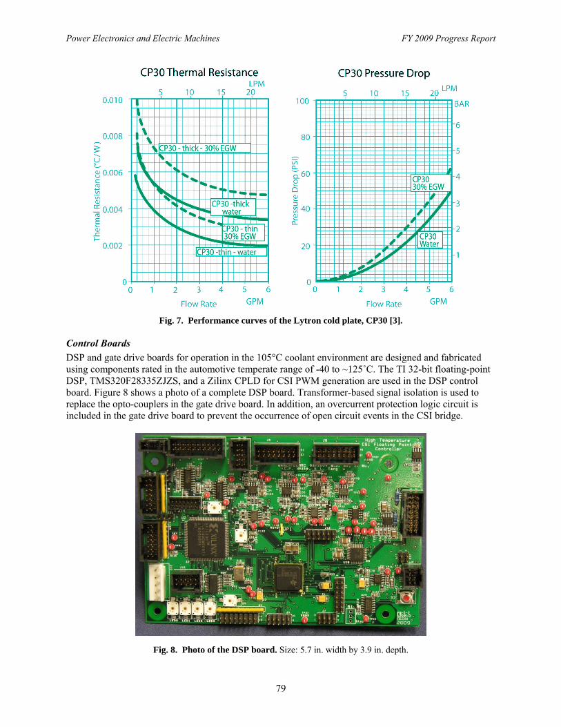
Power Electronics and Electric Machines FY 2009 Progress Report
79
Fig. 7. Performance curves of the Lytron cold plate, CP30 [3]. Control Boards
DSP and gate drive boards for operation in the 105°C coolant environment are designed and fabricated using components rated in the automotive temperate range of -40 to ~125˚C. The TI 32-bit floating-point DSP, TMS320F28335ZJZS, and a Zilinx CPLD for CSI PWM generation are used in the DSP control board. Figure 8 shows a photo of a complete DSP board. Transformer-based signal isolation is used to replace the opto-couplers in the gate drive board. In addition, an overcurrent protection logic circuit is included in the gate drive board to prevent the occurrence of open circuit events in the CSI bridge.
Fig. 8. Photo of the DSP board. Size: 5.7 in. width by 3.9 in. depth.
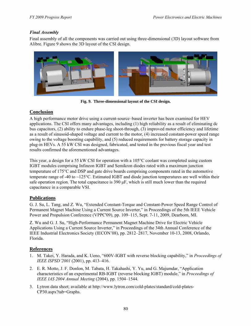
FY 2009 Progress Report Power Electronics and Electric Machines
80
Final Assembly
Final assembly of all the components was carried out using three-dimensional (3D) layout software from Alibre. Figure 9 shows the 3D layout of the CSI design.
Fig. 9. Three-dimensional layout of the CSI design. Conclusion A high performance motor drive using a current-source–based inverter has been examined for HEV applications. The CSI offers many advantages, including (1) high reliability as a result of eliminating dc bus capacitors, (2) ability to endure phase-leg shoot-through, (3) improved motor efficiency and lifetime as a result of sinusoid-shaped voltage and current to the motor, (4) increased constant-power speed range owing to the voltage boosting capability, and (5) reduced requirements for battery storage capacity in plug-in HEVs. A 55 kW CSI was designed, fabricated, and tested in the previous fiscal year and test results confirmed the aforementioned advantages. This year, a design for a 55 kW CSI for operation with a 105°C coolant was completed using custom IGBT modules comprising Infineon IGBT and Semikron diodes rated with a maximum junction temperature of 175°C and DSP and gate drive boards comprising components rated in the automotive temperate range of -40 to ~125°C. Estimated IGBT and diode junction temperatures are well within their safe operation region. The total capacitance is 390 μF, which is still much lower than the required capacitance in a comparable VSI. Publications G. J. Su, L. Tang, and Z. Wu, “Extended Constant-Torque and Constant-Power Speed Range Control of Permanent Magnet Machine Using a Current Source Inverter,” in Proceedings of the 5th IEEE Vehicle Power and Propulsion Conference (VPPC'09), pp. 109–115, Sept. 7-11, 2009, Dearborn, MI.
Z. Wu and G. J. Su, “High-Performance Permanent Magnet Machine Drive for Electric Vehicle Applications Using a Current Source Inverter,” in Proceedings of the 34th Annual Conference of the IEEE Industrial Electronics Society (IECON’08), pp. 2812–2817, November 10-13, 2008, Orlando, Florida. References 1. M. Takei, Y. Harada, and K. Ueno, “600V-IGBT with reverse blocking capability,” in Proceedings of
IEEE ISPSD’2001 (2001), pp. 413–416.
2. E. R. Motto, J. F. Donlon, M. Tabata, H. Takahashi, Y. Yu, and G. Majumdar, “Application characteristics of an experimental RB-IGBT (reverse blocking IGBT) module,” in Proceedings of IEEE IAS 2004 Annual Meeting (2004), pp. 1504–1544.
3. Lytron data sheet; available at http://www.lytron.com/cold-plates/standard/cold-plates-CP30.aspx?tab=Graphs.

Power Electronics and Electric Machines FY 2009 Progress Report
81
Patents Gui-Jia Su, “Power Conversion Apparatus and Method,” application US12/399,486, March 6, 2009, pending.

FY 2009 Progress Report Power Electronics and Electric Machines
82
4.5 Using the Traction Drive Power Electronics System to Provide Plug-In Capability for Hybrid Electric Vehicles
Principal Investigator: Gui-Jia Su Oak Ridge National Laboratory National Transportation Research Center 2360 Cherahala Boulevard Knoxville, TN 37932 Voice: 865-946-1330; Fax: 865-946-1262; E-mail: [email protected] DOE Technology Development Manager: Susan A. Rogers Voice: 202-586-8997; Fax: 202-586-1600; E-mail: [email protected] ORNL Program Manager: Mitch Olszewski Voice: 865-946-1350; Fax: 865-946-1262; E-mail: [email protected] Objectives • Overall project objectives
— Reduce cost and volume by 90% compared with stand-alone battery chargers. — Provide rapid charging capability for use at high-power charging stations. — Enable plug-in hybrid electric vehicles (PHEVs) as mobile power generators. — Investigate hardware and software requirements for implementing smart charging and vehicle-to-
grid capabilities. • Objectives for FY 2009 effort
— Modify and test the hybrid electric vehicle (HEV) power electronics system prototype consisting of a 55 kW motor inverter and a 30 kW generator inverter to evaluate its mobile power generation capability.
— Characterize mobile power generation efficiency performance. Approach • Modify the prototype of a 55 kW motor inverter and a 30 kW generator inverter built in FY 2008 for
mobile power generation operation. • Develop digital signal processing (DSP) code to implement mobile power generation for both battery-
powered and engine-powered operations. • Test and evaluate the prototype’s power generation capability and performance. Major Accomplishments • Designed, fabricated, and successfully tested an HEV power electronics system prototype consisting
of a 55 kW motor inverter and a 30 kW generator inverter for operation as a battery charger and mobile power generator.
• Attained a maximum charging efficiency greater than 95% with a 120 V input and greater than 98% with a 240 V input.
• Attained a grid current harmonic distortion factor less than 9% at 120 V input and less than 7% at 240 V input at rated power during charging operation.
• Attained a maximum efficiency of 80% with a 120 V output in engine-powered generation mode. • Attained a maximum efficiency of 97% at 240 V output and 94% at 120 V output in battery-powered
generation mode.

Power Electronics and Electric Machines FY 2009 Progress Report
83
Future Direction None: Project completed in FY 2009. Technical Discussion Background
PHEVs are emerging as a pre-fuel-cell technology that offers greater potential than hybrid vehicles currently on the market to reduce oil consumption and carbon dioxide emissions. In PHEVs, the energy storage capacity of the battery needs to be increased significantly to enable a driving distance of at least 40 miles in an all-electric mode, the distance needed to substantially reduce oil consumption for daily commuting. A charger is also required to replenish the battery after it is depleted, typically done overnight to leverage energy costs by taking advantage of off-peak electricity rates. Stand-alone battery chargers, however, impose an extra cost on already expensive HEVs and have other limitations. A typical stand-alone battery charger for PHEVs consists of a diode rectifier and a unidirectional dc-dc converter (i.e., it can only charge the battery) that uses power semiconductor switches, diodes, inductors, and capacitors, as shown in Fig. 1. A charger with a low charging capability of 1 to ~3 kW can cost almost 30% as much as the electric traction system for a midsize PHEV-20 car ($690) [1]. The limited charging capability results in a long charging time (about 6 to 8 hours), which could negatively impact the acceptance of PHEVs.
Fig. 1. A schematic showing major components in a stand-alone battery charger. To minimize the cost of the charger, this project is investigating the use of the power electronics and motors already aboard the vehicle to fulfill the charging requirements. It is expected that, compared with a stand-alone battery charger, the proposed approach will impose virtually no additional cost or will significantly reduce the cost, depending on the configuration of the onboard traction drive system. The proposed approach is to integrate the battery charging function into the traction drive system and eliminate or minimize the number of additional components. Because traction power inverters have a greater current-carrying capability, the integrated charger can reduce the charging time significantly. Another benefit of this approach is that it enables PHEVs to function as mobile generators at little or no additional cost. Another objective is to investigate hardware and software requirements for implementing smart charging and vehicle-to-grid capabilities. Description of the Reduced-Part dc-dc Converter
Figure 2 shows topologies for using the onboard electrical drive system to provide plug-in charging and mobile generation capabilities for HEVs. The onboard electrical drive system may consist of one or more electrical motor drive units, all connected to a common dc bus. Each motor drive unit typically uses a three-phase inverter/converter (INV/CONV) and a three-phase motor/generator (MG) with a Y-connection to the motor and the neutral point (NMG) brought out. At least one drive unit is coupled to the engine shaft through a mechanical transmission device. The basic idea is to use the MGs as inductors by connecting their neutral points to an external charging source to charge the battery or to external loads to supply power to them. The external charging source can be a dc or single-phase or multiphase ac power supply, depending on the number of onboard drive units. Figure 2(a) illustrates an arrangement for a
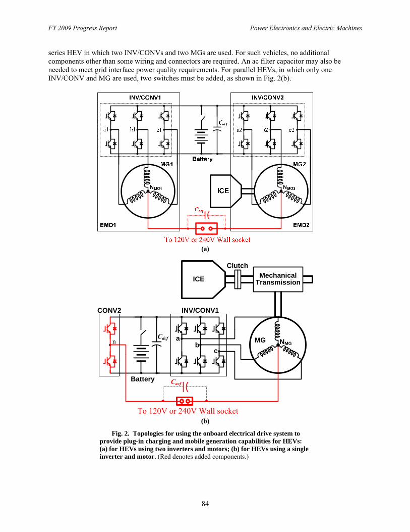
FY 2009 Progress Report Power Electronics and Electric Machines
84
series HEV in which two INV/CONVs and two MGs are used. For such vehicles, no additional components other than some wiring and connectors are required. An ac filter capacitor may also be needed to meet grid interface power quality requirements. For parallel HEVs, in which only one INV/CONV and MG are used, two switches must be added, as shown in Fig. 2(b).
(a)
ab
c
INV/CONV1CONV2
Battery
MG NMG
MechanicalTransmissionICE
Clutch
To 120V or 240V Wall socket
nCdcf
Cacf
(b)
Fig. 2. Topologies for using the onboard electrical drive system to provide plug-in charging and mobile generation capabilities for HEVs: (a) for HEVs using two inverters and motors; (b) for HEVs using a single inverter and motor. (Red denotes added components.)

Power Electronics and Electric Machines FY 2009 Progress Report
85
All the switch legs in each INV/CONV collectively function as a single switch leg and the MG as an inductor. Together, the drive units form a single-phase or multiphase converter, operating in the charging mode, to regulate the dc bus voltage. In the generation mode, the drive units form a single-phase or multiphase inverter to supply external loads. In this mode, the MG of the drive unit coupled to the engine shaft is driven by the engine to generate power to supply the dc bus and ultimately the external loads. Alternatively, power can be drawn from the battery for short operating intervals. Figure 3 shows a schematic of the circuit in Fig. 2(a) during operation in charging mode. All three switch legs (a1, b1, c1 and a2, b2, c2) in INV/CONV1 and INV/CONV2 collectively function as a single switch leg, and the MGs function as two impedance networks. The MG stators comprise zero sequence impedance networks, ZSIN1 and ZSIN2. Each ZSIN consists of three branches and each branch comprises the stator winding phase resistance (Rms1 or Rms2) and the stator phase leakage inductance (lm0s1 or lm0s2). Together, the two drive units form a single-phase converter to regulate the battery voltage, Vbat, or the charging current, Ibat. Normally, the single-phase converter is controlled so as to maintain a unity power factor by keeping the source current, is, in phase with the source voltage, vs. An additional benefit of operating the three-phase converters as single leg converters is the reduction in harmonic current components resulting from interleaving the gating signals of the three legs.
MG1 NMG1
ia1 ib1 ic1
Rms1
lm0s1
MG2NMG2
ia2 ib2 ic2
Rms2
lm0s2
a1b1 c1
Cdcf
Battery
S1a
S1b
S1c
S1d
S1e
S1f
INV/CONV1
S2a
S2b
S2c
S2d
S2e
S2f
INV/CONV2
a2b2 c2
Vbat
vs
Ibat
is
ZSIN2ZSIN1 Cacf
Fig. 3. Schematic of a circuit for battery charging mode. Figure 4 shows a schematic of the circuit in Fig. 2(a) during operation in mobile generation mode. There are two available power sources, the battery and the engine. Figure 4(a) illustrates the case in which the battery is the source. In this case, all three switch legs in each of the two INV/CONVs collectively function as a single switch leg and the MGs as two impedance networks. Together the two drive units form a single-phase inverter to regulate the load voltage, vLoad. Figure 4(b) illustrates the case in which power is generated by the MG2 driven by the engine. In this case, the three switch legs in INV/CONV1 collectively function as the first single switch leg of a single-phase inverter and the MG1 functions as an impedance network. INV/CONV2 has dual functions. It first operates as a three-phase converter to regulate the dc bus voltage, Vdc, by drawing power from the generator; at the same time, its three phase legs collectively form the second switch leg of the single-phase inverter to regulate the load voltage, vLoad.

FY 2009 Progress Report Power Electronics and Electric Machines
86
(a)
a1b1 c1
Cdcf
Battery
S1a
S1b
S1c
S1d
S1e
S1f
INV/CONV1
S2a
S2b
S2c
S2d
S2e
S2f
INV/CONV2
a2b2 c2
NMG2
ic2
ib2
ia2
Rms2lm0s2
NMG2
ZSIN2vLoad
iLoad
MG1 NMG1
ia1 ib1 ic1
Rms1
lm0s1
Load
ICE
MG2
Vdc
Cacf
(b)
Fig. 4. Schematic of circuits for mobile generator mode: (a) battery-powered generation mode (i.e., using the battery as the power source); (b) engine-powered generation mode (i.e., using the motor MG2 driven by the engine as the power source).
Prototype Modification and Testing
An HEV drive inverter system prototype consisting of a 55 kW motor inverter and a 30 kW generator inverter with a plug-in charging capability of 20 kW was designed, built, and tested in charging operation

Power Electronics and Electric Machines FY 2009 Progress Report
87
in FY 2008. Figure 5 is a photo of the prototype. The 55 kW motor inverter was implemented with a six-pack insulated gate bipolar transistor (IGBT) module rated at 600 V and 600 A (part number PM600CLA060 from Powerex), and the 30 kW generator inverter was implemented with a six-pack IGBT module rated at 600 V and 300 A (part number PM300CLA060 from the same vendor). The bus capacitor bank was constructed using four film capacitors (Electronic Concepts, Inc., part number UP33BC0375), rated at 600 Vdc and 375 μF. These components are mounted on a 12 × 7 in. cold plate. The prototype was modified by adding a voltage sensor and signal conditioning circuitry and tested operating in the mobile generator mode.
Fig. 5. A photo of a prototype consisting of a 55 kW motor inverter and a 30 kW generator inverter with plug-in charging and mobile power generation capabilities. The heat sink footprint is 12 in. width by 7 in. depth.
DSP code was then developed to implement the mobile power generation control algorithms for both battery-powered and engine-powered operations. Figure 6 shows control block diagrams for mobile power generation. In 6(a) the system operates in the engine-powered generation mode using the motor MG2 driven by the engine as the power source. Using the field orientation technique and space vector pulse-width modulation (PWM) method, the d and q axis currents, idM and iqM, of MG2 are controlled with the motor inverter to maintain the inverter dc bus voltage at the commanded level, V*
DC. The generator inverter is used to control the output voltage with the help of an inner current loop to improve the dynamic response. Both synchronized and interleaved PWM schemes were used for the generator inverter to investigate the impact on the efficiency by the switching schemes. Due to the PWM generation hardware limitation of the digital signal processor, a software implementation of the interleaved PWM based on a single carrier was developed. In 6(b) the system operates in battery-powered generation mode using the high voltage battery as the power source. Both inverters are used to control the output voltage
To generator To motor
Generator inverter
Motor inverter
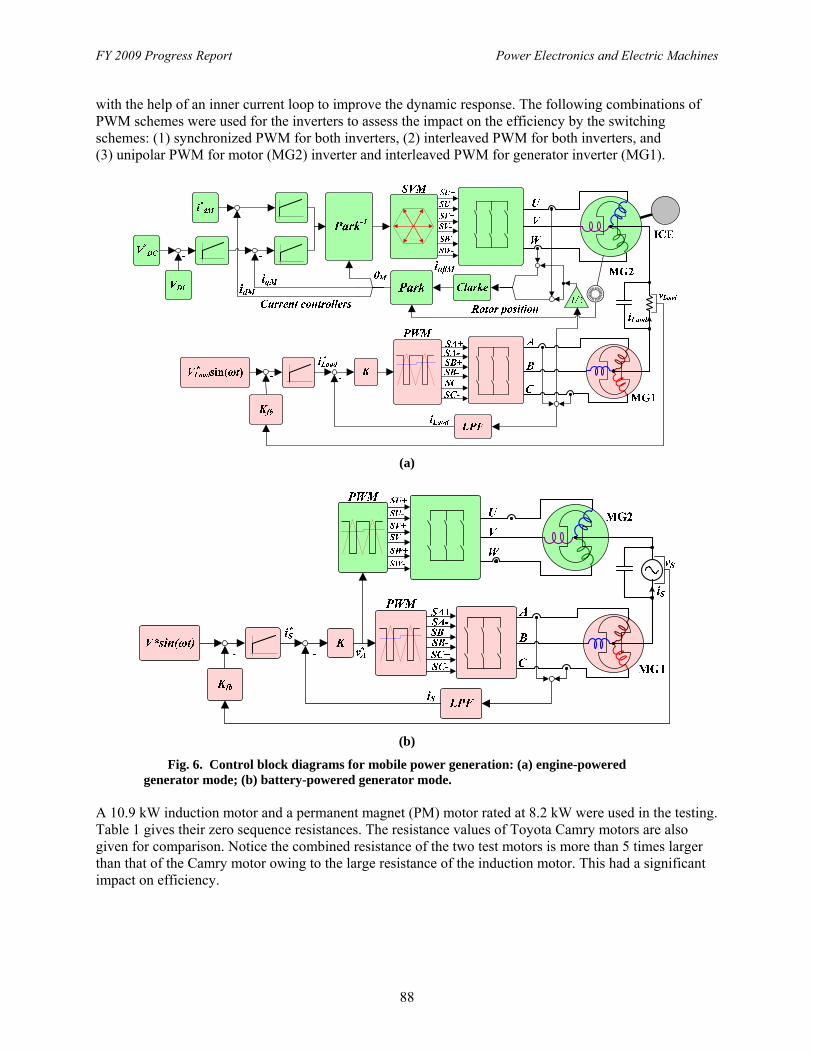
FY 2009 Progress Report Power Electronics and Electric Machines
88
with the help of an inner current loop to improve the dynamic response. The following combinations of PWM schemes were used for the inverters to assess the impact on the efficiency by the switching schemes: (1) synchronized PWM for both inverters, (2) interleaved PWM for both inverters, and (3) unipolar PWM for motor (MG2) inverter and interleaved PWM for generator inverter (MG1).
(a)
(b)
Fig. 6. Control block diagrams for mobile power generation: (a) engine-powered generator mode; (b) battery-powered generator mode.
A 10.9 kW induction motor and a permanent magnet (PM) motor rated at 8.2 kW were used in the testing. Table 1 gives their zero sequence resistances. The resistance values of Toyota Camry motors are also given for comparison. Notice the combined resistance of the two test motors is more than 5 times larger than that of the Camry motor owing to the large resistance of the induction motor. This had a significant impact on efficiency.

Power Electronics and Electric Machines FY 2009 Progress Report
89
Table 1. Motor Zero Sequence Resistance
Test motor 1 165.74 mΩ Camry generator 21.58 mΩ Test motor 2 23.8 mΩ Camry motor 10.75 mΩ Combined 189.54 mΩ Combined 32.32 mΩ
The prototype was tested in engine-power generation mode with 120 V output and battery-powered generation mode at 120 V and 240 V output for varying resistive load power. Figure 7 illustrates test results showing operating waveforms in the engine-powered generator mode. The smooth sinusoidal output voltage and current waveforms and flat dc bus voltage indicate excellent performance of the controller. Because one-third of the 60 Hz load current is superimposed as a zero-sequence component on the original generator current, the generator phase currents are no longer sinusoidal. Figure 8 plots measured efficiency against output power. Due to the relatively low efficiency (<85%) of the small PM generator, the system efficiency does not exceed 80%. However, it is estimated that a maximum efficiency greater than 92% could be achieved with a production PM generator efficiency of 95% because the inverter efficiency can reach 97%, as will be shown later. In addition, a 1% improvement is attained with the interleaved switching over the synchronized switching. Figure 9 illustrates test results showing operating waveforms in the battery-powered generator mode, where the output voltage is set at 120 V in 9(a) and 240 V in 9(b). Again, the smooth sinusoidal output voltage and current waveforms and flat dc bus voltage in both output voltages indicate excellent performance of the control method. In this operation mode, both motors are used as inductors and one-third of the 60 Hz load current is flowing in each phase winding as a zero-sequence component, as indicated by the identical two-motor phase currents in the test results. Figure 10 plots measured efficiency against output power. At the output voltage of 240 Vac as shown in 10(a), significant efficiency improvement is achieved with the interleaved and unipolar switching over the synchronized switching PWM scheme due to the significant reduction of switching loss through the interleaved and uniploar switching method. The maximum efficiency reaches 97% at the output power of 6.2 kW. Figure 10(b) shows the measured efficiency at the output voltage of 120 Vac with the interleaving and unipolar switching scheme. The maximum efficiency in this case is 94% at the output power of 2.1 kW. It is observed in both cases that the efficiency drops as the output power increases due to substantial copper loss at high load current in the high stator resistance of the test motors. This efficiency decrease is faster in the case of 120 V output because at a given output power the current is larger than in the 240 V output, which in turn generates even larger copper loss in the form of I2R. It is therefore expected that much better efficiency could be attained with production PM motors whose resistance is much lower than those of the test motors.
FY 2009 Progress Report Power Electronics and Electric Machines
90
DC bus voltage: 500V/div
Generator U and W phase currents: 100A/div
Output voltage: 200V/div Output current: 100A/div
(a)
DC bus voltage: 500V/div
Generator U and W phase currents: 100A/div
Output voltage: 200V/div Output current: 100A/div
(b)
Fig. 7. Test results showing operation in engine-powered generator mode for (a) output power = 3.0 kW at 120V and (b) output power = 5.0 kW at 120 V.
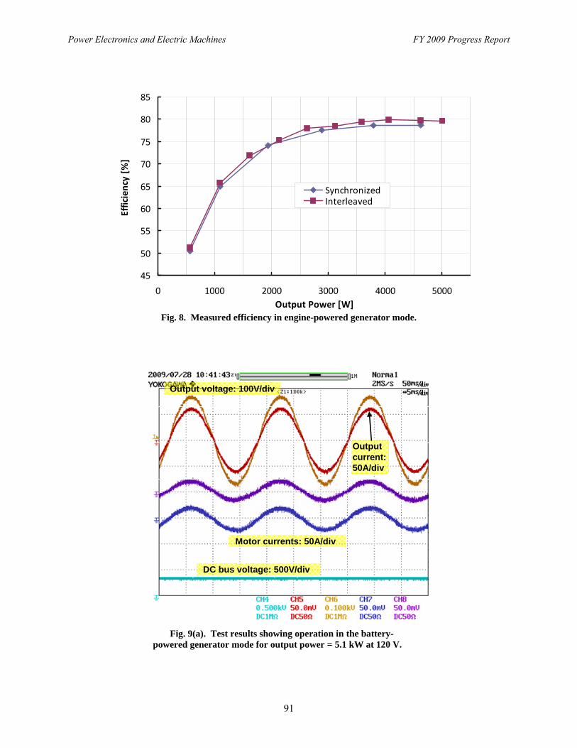
Power Electronics and Electric Machines FY 2009 Progress Report
91
45
50
55
60
65
70
75
80
85
0 1000 2000 3000 4000 5000Output Power [W]
Effic
ienc
y [%
]
Synchronized Interleaved
Fig. 8. Measured efficiency in engine-powered generator mode.
DC bus voltage: 500V/div
Motor currents: 50A/div
Output voltage: 100V/div
Output current: 50A/div
DC bus voltage: 500V/div
Motor currents: 50A/div
Output voltage: 100V/div
Output current: 50A/div
Fig. 9(a). Test results showing operation in the battery-powered generator mode for output power = 5.1 kW at 120 V.
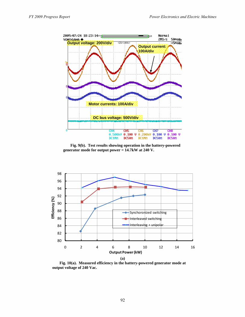
FY 2009 Progress Report Power Electronics and Electric Machines
92
DC bus voltage: 500V/div
Motor currents: 100A/div
Output voltage: 200V/divOutput current: 100A/div
DC bus voltage: 500V/div
Motor currents: 100A/div
Output voltage: 200V/divOutput current: 100A/div
Fig. 9(b). Test results showing operation in the battery-powered generator mode for output power = 14.7kW at 240 V.
80
82
84
86
88
90
92
94
96
98
0 2 4 6 8 10 12 14 16
Effic
ienc
y (%
)
Output Power (kW)
Synchoronized switching
Interleaved switching
Interleaving + unipolar
(a)
Fig. 10(a). Measured efficiency in the battery-powered generator mode at output voltage of 240 Vac.

Power Electronics and Electric Machines FY 2009 Progress Report
93
85
86
87
88
89
90
91
92
93
94
95
0 1 2 3 4 5 6 7
Output power [kW]
Eff
icie
ncy
[%
]
Fig. 10(b). Measured efficiency in the battery-powered generator mode at output voltage of 120 Vac.
Conclusion This project explored ways of using the onboard electrical drive system in different HEV configurations to provide plug-in charging and mobile power generation capabilities. The proposed charging schemes offer many benefits, including (1) significantly reducing the cost and volume of battery chargers in PHEVs, (2) providing rapid charging capability, and (3) enabling the use of PHEVs as mobile generators. Detailed circuit simulations were first carried out, and the simulation results proved the concepts and validated the rapid charging and mobile generation capabilities. An HEV power electronics system prototype made up of a 55 kW motor inverter and a 30 kW generator inverter was designed, fabricated, and successfully tested in FY 2008 for operation as a battery charger. Test results confirmed high efficiency, high power factor, and low harmonic distortion in the charging mode. The prototype was modified and successfully tested during FY 2009 as a mobile power generator. Test results show high efficiency with the proposed PWM switching scheme. • Attained a maximum efficiency of 97% at 240 V output and 94% at 120 V output in the
battery-powered generation mode. • Attained a maximum efficiency of 80% with a 120 V output in engine-powered generation mode. Publications L. Tang and G. J. Su, “A Low-Cost, Digitally-Controlled Charger for Plug-In Hybrid Electric Vehicles,” IEEE Energy Conversion Congress and Exposition (ECCE), September 20—24, 2009, San Jose, California, pp. 3923–3929. References 1. Advanced Batteries for Electric-Drive Vehicles, Report 1009299, Electric Power Research Institute,
May 2004.
2. Electric Auto Association Plug-in Hybrid Electric Vehicle, “Battery chargers, PHEV applications,” http://www.eaa-phev.org/wiki/Battery_Chargers.

FY 2009 Progress Report Power Electronics and Electric Machines
94
Patents Gui-Jia Su, “Electric Vehicle System for Charging and Supplying Electrical Power,” Patent Application US2008/0094013A1, pending.

Power Electronics and Electric Machines FY 2009 Progress Report
95
4.6 A Segmented Drive System with a Small DC Bus Capacitor
Principal Investigator: Gui-Jia Su Oak Ridge National Laboratory National Transportation Research Center 2360 Cherahala Boulevard Knoxville, TN 37932 Voice: 865-946-1330; Fax: 865-946-1262; E-mail: [email protected] DOE Technology Development Manager: Susan A. Rogers Voice: 202-586-8997; Fax: 202-586-1600; E-mail: [email protected] ORNL Program Manager: Mitch Olszewski Voice: 865-946-1350; Fax: 865-946-1262; E-mail: [email protected] Objectives • Overall project objectives
— Significantly reduce the amount of inverter dc bus capacitance by reducing the ripple current by more than 60%.
• Objectives for FY 2009 effort — Perform a simulation study to prove the concept. — Assess the effect of various pulse-width modulation (PWM) schemes on the reduction of ripple
current to determine the optimal PWM method. — Conduct a conceptual design for a 55 kW prototype.
Approach • Use a segmented drive system topology that does not need additional switches or passive components
but will enable the use of optimized PWM schemes to significantly reduce the dc link ripple current and thus the capacitance.
• Perform studies of various carrier-based and space-vector PWM techniques using PSIM simulation software to assess their impact on the capacitor ripple current.
• Build and test a 55 kW prototype (in FY 2010) to experimentally validate the simulation study. Major Accomplishments • Validated the segmented drive concept by a simulation study. • Achieved more than 65% reduction in capacitor ripple current as compared to the standard inverter
configuration. • Achieved 80% reduction in battery ripple current. • Achieved 70% reduction in dc bus ripple voltage. • Achieved 50% reduction in motor ripple current. • Completed a conceptual design for a 55 kW prototype. Future Direction • Finalize the design; build and test a 55 kW prototype. • Apply the segmented drive concept in an integrated traction drive system.
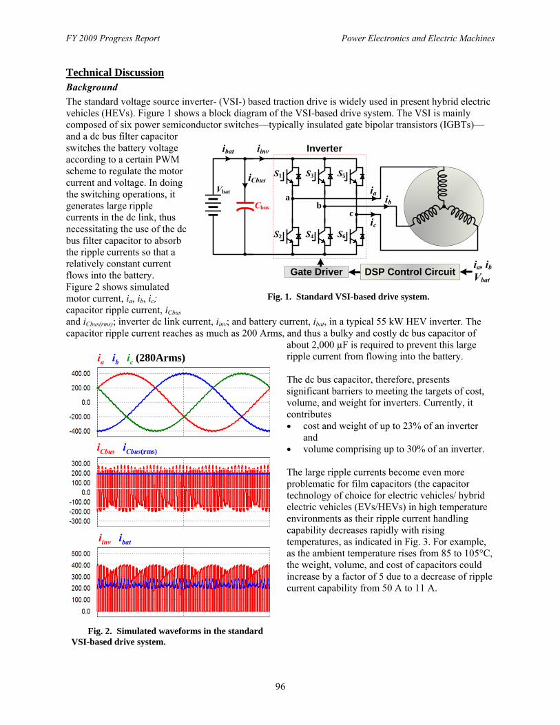
FY 2009 Progress Report Power Electronics and Electric Machines
96
Technical Discussion Background
The standard voltage source inverter- (VSI-) based traction drive is widely used in present hybrid electric vehicles (HEVs). Figure 1 shows a block diagram of the VSI-based drive system. The VSI is mainly composed of six power semiconductor switches—typically insulated gate bipolar transistors (IGBTs)—and a dc bus filter capacitor switches the battery voltage according to a certain PWM scheme to regulate the motor current and voltage. In doing the switching operations, it generates large ripple currents in the dc link, thus necessitating the use of the dc bus filter capacitor to absorb the ripple currents so that a relatively constant current flows into the battery. Figure 2 shows simulated motor current, ia, ib, ic; capacitor ripple current, iCbus and iCbus(rms); inverter dc link current, iinv; and battery current, ibat, in a typical 55 kW HEV inverter. The capacitor ripple current reaches as much as 200 Arms, and thus a bulky and costly dc bus capacitor of
about 2,000 µF is required to prevent this large ripple current from flowing into the battery. The dc bus capacitor, therefore, presents significant barriers to meeting the targets of cost, volume, and weight for inverters. Currently, it contributes • cost and weight of up to 23% of an inverter
and • volume comprising up to 30% of an inverter. The large ripple currents become even more problematic for film capacitors (the capacitor technology of choice for electric vehicles/ hybrid electric vehicles (EVs/HEVs) in high temperature environments as their ripple current handling capability decreases rapidly with rising temperatures, as indicated in Fig. 3. For example, as the ambient temperature rises from 85 to 105°C, the weight, volume, and cost of capacitors could increase by a factor of 5 due to a decrease of ripple current capability from 50 A to 11 A.
cb
aia
ib
Inverter
S1
S2
S3
S4
S5
S6
ic
Cbus
Vbat
Gate Driver
iCbus
ibat iinv
ia, ib
VbatDSP Control Circuit
Fig. 1. Standard VSI-based drive system.
iCbus iCbus(rms)
iinv ibat
ia ib ic (280Arms)
iCbus iCbus(rms)
iinv ibat
ia ib ic (280Arms)
Fig. 2. Simulated waveforms in the standard VSI-based drive system.
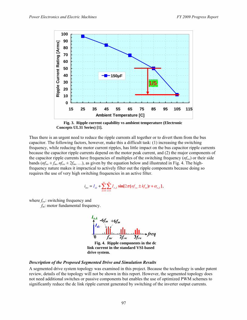
Power Electronics and Electric Machines FY 2009 Progress Report
97
0
10
20
30
40
50
60
70
80
90
100
15 25 35 45 55 65 75 85 95 105 115
Ambient Temperature [C]
Rip
ple
Cu
rren
t R
atin
g [
Arm
s]
150µF
1/5
Fig. 3. Ripple current capability vs ambient temperature (Electronic
Concepts UL31 Series) [1]. Thus there is an urgent need to reduce the ripple currents all together or to divert them from the bus capacitor. The following factors, however, make this a difficult task: (1) increasing the switching frequency, while reducing the motor current ripples, has little impact on the bus capacitor ripple currents because the capacitor ripple currents depend on the motor peak current, and (2) the major components of the capacitor ripple currents have frequencies of multiples of the switching frequency (nfsw) or their side bands (nfsw ± fm, nfsw ± 2fm, …), as given by the equation below and illustrated in Fig. 4. The high-frequency nature makes it impractical to actively filter out the ripple components because doing so requires the use of very high switching frequencies in an active filter.
0 1
2, ,sin[ ( ) ]n k swd m n kk n
in cv I nf k tI fi π α∞ ∞
= =
±= ++ ,
where fsw: switching frequency and
fm: motor fundamental frequency.
Fig. 4. Ripple components in the dc
link current in the standard VSI-based drive system.
Description of the Proposed Segmented Drive and Simulation Results
A segmented drive system topology was examined in this project. Because the technology is under patent review, details of the topology will not be shown in this report. However, the segmented topology does not need additional switches or passive components but enables the use of optimized PWM schemes to significantly reduce the dc link ripple current generated by switching of the inverter output currents.
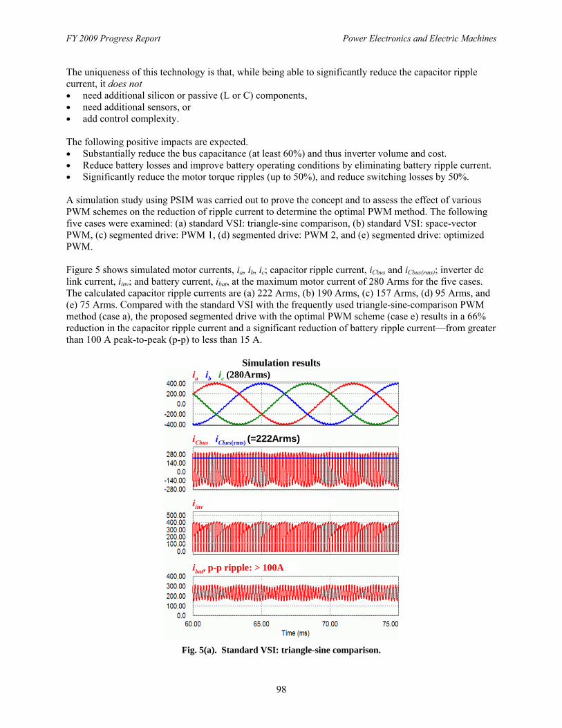
FY 2009 Progress Report Power Electronics and Electric Machines
98
The uniqueness of this technology is that, while being able to significantly reduce the capacitor ripple current, it does not • need additional silicon or passive (L or C) components, • need additional sensors, or • add control complexity. The following positive impacts are expected. • Substantially reduce the bus capacitance (at least 60%) and thus inverter volume and cost. • Reduce battery losses and improve battery operating conditions by eliminating battery ripple current. • Significantly reduce the motor torque ripples (up to 50%), and reduce switching losses by 50%. A simulation study using PSIM was carried out to prove the concept and to assess the effect of various PWM schemes on the reduction of ripple current to determine the optimal PWM method. The following five cases were examined: (a) standard VSI: triangle-sine comparison, (b) standard VSI: space-vector PWM, (c) segmented drive: PWM 1, (d) segmented drive: PWM 2, and (e) segmented drive: optimized PWM. Figure 5 shows simulated motor currents, ia, ib, ic; capacitor ripple current, iCbus and iCbus(rms); inverter dc link current, iinv; and battery current, ibat, at the maximum motor current of 280 Arms for the five cases. The calculated capacitor ripple currents are (a) 222 Arms, (b) 190 Arms, (c) 157 Arms, (d) 95 Arms, and (e) 75 Arms. Compared with the standard VSI with the frequently used triangle-sine-comparison PWM method (case a), the proposed segmented drive with the optimal PWM scheme (case e) results in a 66% reduction in the capacitor ripple current and a significant reduction of battery ripple current—from greater than 100 A peak-to-peak (p-p) to less than 15 A.
Simulation results ia ib ic (280Arms)
iCbus iCbus(rms) (=222Arms)
iinv
ibat, p-p ripple: > 100A
ia ib ic (280Arms)
iCbus iCbus(rms) (=222Arms)
iinv
ibat, p-p ripple: > 100A
Fig. 5(a). Standard VSI: triangle-sine comparison.
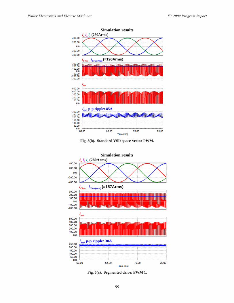
Power Electronics and Electric Machines FY 2009 Progress Report
99
Simulation results ia ib ic (280Arms)
iCbus iCbus(rms) (=190Arms)
iinv
ibat, p-p ripple: 85A
Fig. 5(b). Standard VSI: space-vector PWM.
Simulation results ia ib ic (280Arms)
iCbus iCbus(rms) (=157Arms)
iinv
ibat, p-p ripple: 30A
Fig. 5(c). Segmented drive: PWM 1.
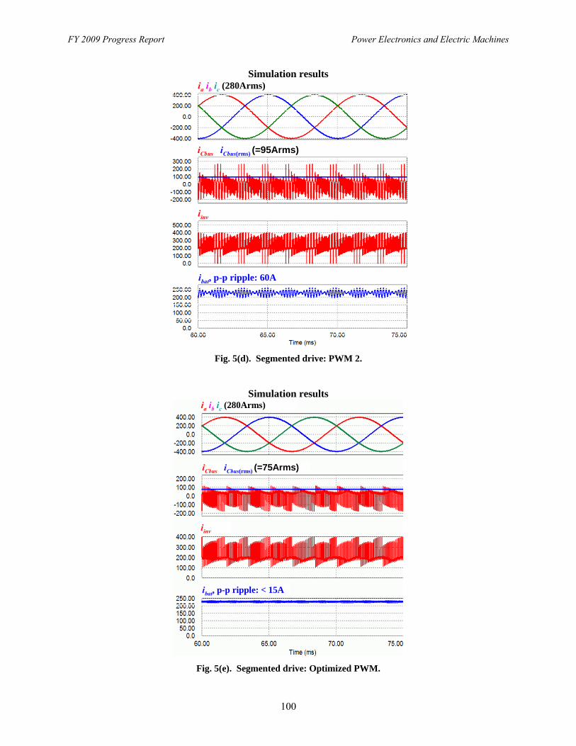
FY 2009 Progress Report Power Electronics and Electric Machines
100
Simulation results ia ib ic (280Arms)
iCbus iCbus(rms) (=95Arms)
iinv
ibat, p-p ripple: 60A
Fig. 5(d). Segmented drive: PWM 2.
Simulation results
iCbus iCbus(rms) (=75Arms)
iinv
ia ib ic (280Arms)
ibat, p-p ripple: < 15A
iCbus iCbus(rms) (=75Arms)
iinv
ia ib ic (280Arms)
ibat, p-p ripple: < 15A
Fig. 5(e). Segmented drive: Optimized PWM.
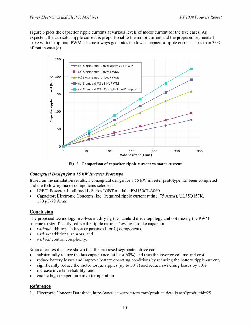
Power Electronics and Electric Machines FY 2009 Progress Report
101
Figure 6 plots the capacitor ripple currents at various levels of motor current for the five cases. As expected, the capacitor ripple current is proportional to the motor current and the proposed segmented drive with the optimal PWM scheme always generates the lowest capacitor ripple current—less than 35% of that in case (a).
0
50
100
150
200
250
0 50 100 150 200 250 300Motor c urrent (Arms )
Cap
cito
r ri
pp
le c
urr
ent (
Arm
s)
(e) S egmented D rive: Optimized P WM
(d) S egmented D rive: P WM2
(c) S egmented D rive: P WM1
(b) S tandard V S I: S P V P WM
(a) S tandard V S I: Triangle-S ine-C omparion
Fig. 6. Comparison of capacitor ripple current vs motor current. Conceptual Design for a 55 kW Inverter Prototype
Based on the simulation results, a conceptual design for a 55 kW inverter prototype has been completed and the following major components selected. • IGBT: Powerex Intellimod L-Series IGBT module, PM150CLA060 • Capacitor; Electronic Concepts, Inc. (required ripple current rating, 75 Arms), UL35Q157K,
150 µF/78 Arms Conclusion The proposed technology involves modifying the standard drive topology and optimizing the PWM scheme to significantly reduce the ripple current flowing into the capacitor • without additional silicon or passive (L or C) components, • without additional sensors, and • without control complexity. Simulation results have shown that the proposed segmented drive can • substantially reduce the bus capacitance (at least 60%) and thus the inverter volume and cost, • reduce battery losses and improve battery operating conditions by reducing the battery ripple current, • significantly reduce the motor torque ripples (up to 50%) and reduce switching losses by 50%, • increase inverter reliability, and • enable high temperature inverter operation. Reference 1. Electronic Concept Datasheet, http://www.eci-capacitors.com/product_details.asp?productid=29.

Power Electronics and Electric Machines FY 2009 Progress Report
103
5. Systems Research and Technology Development
5.1 Benchmarking of Competitive Technologies
Principal Investigator: Tim Burress Oak Ridge National Laboratory National Transportation Research Center 2360 Cherahala Boulevard Knoxville, TN 37932 Voice: 865-946-1216; Fax: 865-946-1262; E-mail: [email protected] DOE Technology Development Manager: Susan A. Rogers Voice: 202-586-8997; Fax: 202-586-1600; E-mail: [email protected] ORNL Program Manager: Mitch Olszewski Voice: 865-946-1350; Fax: 865-946-1262; E-mail: [email protected] Objectives • Determine the status of nondomestic hybrid electric vehicle (HEV) technologies through assessment
of design, packaging, fabrication, and performance during comprehensive evaluations. — Compare results with other HEV technologies. — Distribute findings in open literature.
• Support FreedomCAR program planning and assist in guiding research efforts. — Confirm validity of the program technology targets. — Provide insight for program direction.
• Produce a technical basis that aids in modeling/designing. • Foster collaborations with Electrical and Electronics Technical Team (EETT) and Vehicle Systems
Analysis Technical Team (VSATT). — Identify unique permanent magnet (PM) synchronous motor/inverter/converter/drive-train
technologies. — Ascertain what additional testing is needed to support research and development.
Approach • Choose vehicle subsystem.
— Evaluate potential benchmarking value of various HEVs. — Consult with original equipment manufacturers (OEMs) as to which system is most beneficial.
• Tear down power control unit (PCU) and electronically controlled continuously variable transmission (ECVT). — Determine volume, weight, specific power, and power density. — Assess design and packaging improvements.
• Prepare components for experimental evaluation. — Develop interface and control algorithm. — Design and fabricate hardware necessary to conduct tests. — Instrument subsystems with measurement devices.
• Evaluate hybrid subsystems. — Determine peak and continuous operation capabilities. — Evaluate efficiencies of subsystems. — Analyze thermal data to determine assorted characteristics.

FY 2009 Progress Report Power Electronics and Electric Machines
104
Major Accomplishments • Conducted end-of-life (EOL) assessments to find and explore any detrimental impacts sustained over
the life of a 2004 Toyota Prius. • Compared observations from EOL assessments to those made during original benchmarking of the
2004 Prius. • Determined that subcomponents of the 2004 Toyota Prius sustained no substantially negative
impacts. • Selected the 2010 Toyota Prius (Generation 3) hybrid system to be benchmarked for the latter portion
of FY 2009 and FY 2010. • Conducted preliminary design/packaging studies of the 2010 Prius PCU and ECVT, wherein
significant differences with respect to the 2004 Toyota Prius were noted. • Assessed mass and volume of various PCU/ECVT components. • Communicated effectively with EETT and VSATT to aid in discerning project direction, test plan,
and test results. Future Direction • Discussions will be conducted with EETT and VSATT to determine the appropriate system to study
in the latter part of FY 2010. • Approaches similar to that of previous benchmarking studies will be taken while working to suit the
universal need for standardized testing conditions. Technical Discussion Benchmarking efforts made in FY 2009 can be categorized under two main groupings. Most of the FY 2009 effort was devoted to conducting EOL assessments of the 2004 Toyota Prius. Secondary efforts were made in the latter portion of FY 2009 to initiate benchmarking assessments of the 2010 Toyota Prius (Generation 3) End-of-Life Assessments
To ascertain the impacts of lifelong operation upon the subcomponents of the 2004 Toyota Prius, used vehicle components from a properly serviced vehicle were needed. Studies in which data are collected from various in-service company fleet vehicles are conducted by Idaho National Laboratory (INL) and Electric Transportation Applications (ETA). The vehicles are operated for 160,000 miles before they are removed from the fleet and are serviced per OEM recommendations. Therefore, collaboration was established through James Francfort at INL to obtain the 2004 Toyota Prius subcomponents and subsequent data from vehicles for which this evaluation process had been completed. The PCU and transaxle were obtained to conduct comprehensive assessments of the subcomponents, allowing observation of any degradation or signs suggestive of deviations from normal operation. PCU components that were studied included the primary capacitor, power electronics (PEs), cold plate, thermal paste, and heat exchanger. Shown in Fig. 1 are the thermocouple locations used during capacitor tests, wherein “X” and “Y” thermocouples were placed on the casing of the capacitor above the main capacitor section of the module. Ripple current tests were conducted on the EOL module as well as on an unused module. (Fig. 2 shows the results of these tests.) As ripple current was applied to the capacitor, the temperature response was monitored over extended periods. The modules were located inside an environmental chamber as the ambient temperature was regulated to maintain consistency throughout the tests. At the beginning of the tests, 50 amps (A) root mean square (RMS) of sinusoidal current was applied to the capacitor for roughly 30 minutes. Thereafter, the current was increased by 50 A for each 30-minute interval, with a final RMS current of 200 A. The traces for the EOL module are shown in colors of cyan and red, which reflect the “X” and “Y” thermocouples, respectively. Note that data from two separate tests are combined on this graph, and the current was not adjusted at exactly 1,800-second
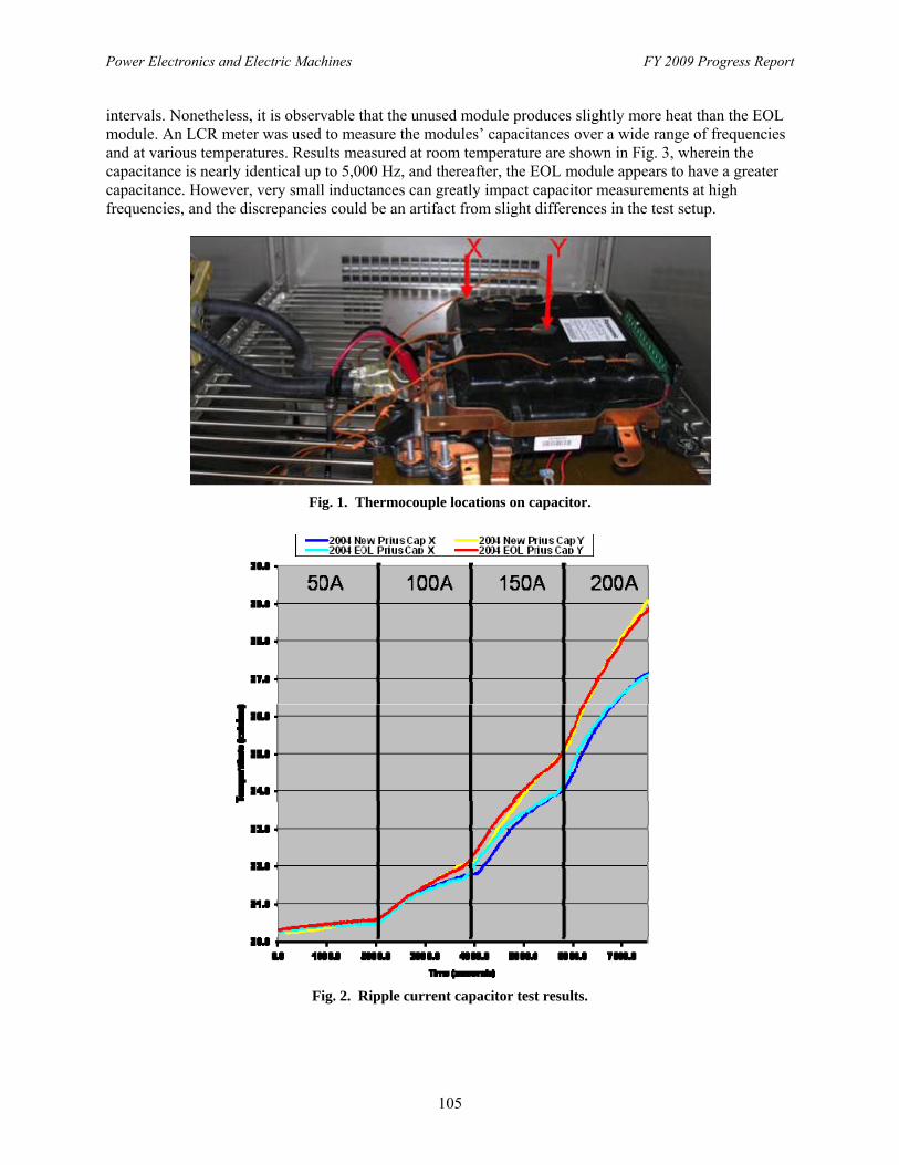
Power Electronics and Electric Machines FY 2009 Progress Report
105
intervals. Nonetheless, it is observable that the unused module produces slightly more heat than the EOL module. An LCR meter was used to measure the modules’ capacitances over a wide range of frequencies and at various temperatures. Results measured at room temperature are shown in Fig. 3, wherein the capacitance is nearly identical up to 5,000 Hz, and thereafter, the EOL module appears to have a greater capacitance. However, very small inductances can greatly impact capacitor measurements at high frequencies, and the discrepancies could be an artifact from slight differences in the test setup.
Fig. 1. Thermocouple locations on capacitor.
Fig. 2. Ripple current capacitor test results.
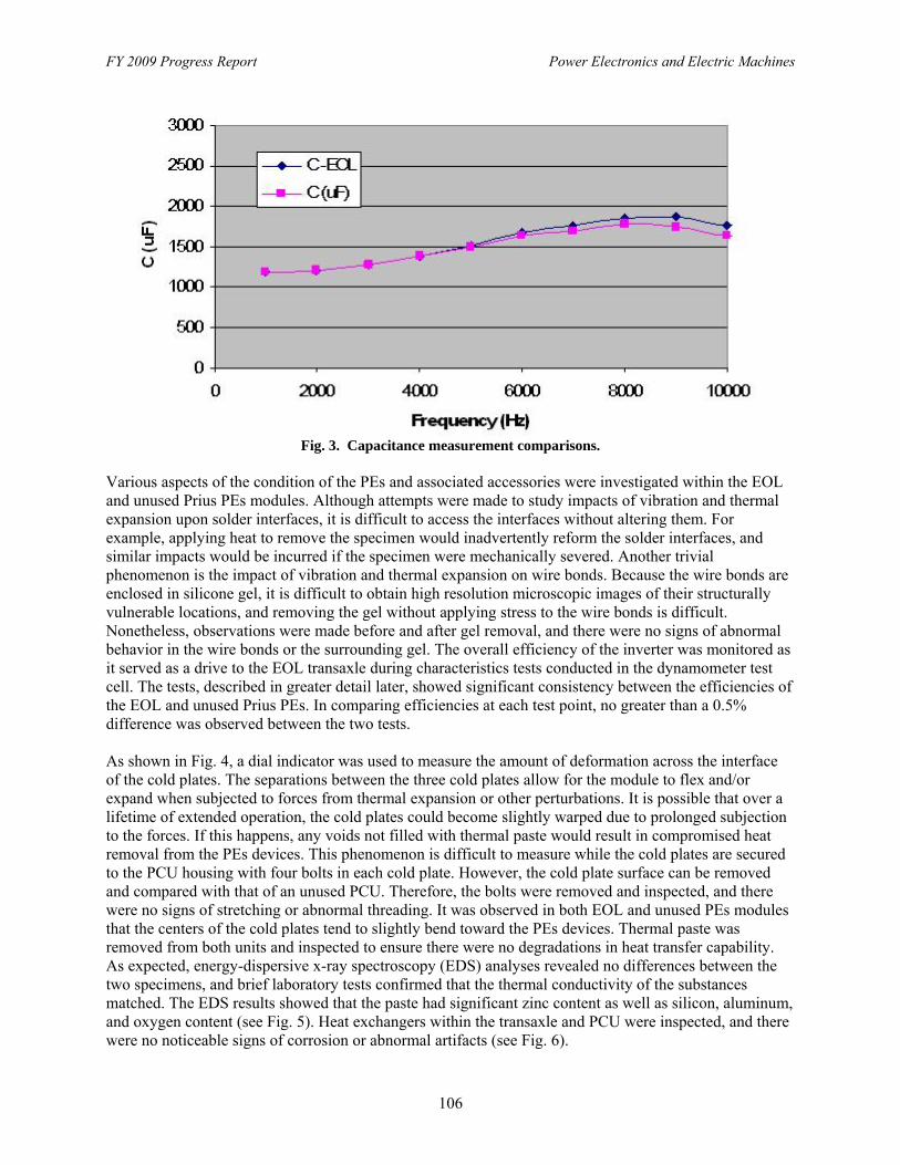
FY 2009 Progress Report Power Electronics and Electric Machines
106
Fig. 3. Capacitance measurement comparisons.
Various aspects of the condition of the PEs and associated accessories were investigated within the EOL and unused Prius PEs modules. Although attempts were made to study impacts of vibration and thermal expansion upon solder interfaces, it is difficult to access the interfaces without altering them. For example, applying heat to remove the specimen would inadvertently reform the solder interfaces, and similar impacts would be incurred if the specimen were mechanically severed. Another trivial phenomenon is the impact of vibration and thermal expansion on wire bonds. Because the wire bonds are enclosed in silicone gel, it is difficult to obtain high resolution microscopic images of their structurally vulnerable locations, and removing the gel without applying stress to the wire bonds is difficult. Nonetheless, observations were made before and after gel removal, and there were no signs of abnormal behavior in the wire bonds or the surrounding gel. The overall efficiency of the inverter was monitored as it served as a drive to the EOL transaxle during characteristics tests conducted in the dynamometer test cell. The tests, described in greater detail later, showed significant consistency between the efficiencies of the EOL and unused Prius PEs. In comparing efficiencies at each test point, no greater than a 0.5% difference was observed between the two tests. As shown in Fig. 4, a dial indicator was used to measure the amount of deformation across the interface of the cold plates. The separations between the three cold plates allow for the module to flex and/or expand when subjected to forces from thermal expansion or other perturbations. It is possible that over a lifetime of extended operation, the cold plates could become slightly warped due to prolonged subjection to the forces. If this happens, any voids not filled with thermal paste would result in compromised heat removal from the PEs devices. This phenomenon is difficult to measure while the cold plates are secured to the PCU housing with four bolts in each cold plate. However, the cold plate surface can be removed and compared with that of an unused PCU. Therefore, the bolts were removed and inspected, and there were no signs of stretching or abnormal threading. It was observed in both EOL and unused PEs modules that the centers of the cold plates tend to slightly bend toward the PEs devices. Thermal paste was removed from both units and inspected to ensure there were no degradations in heat transfer capability. As expected, energy-dispersive x-ray spectroscopy (EDS) analyses revealed no differences between the two specimens, and brief laboratory tests confirmed that the thermal conductivity of the substances matched. The EDS results showed that the paste had significant zinc content as well as silicon, aluminum, and oxygen content (see Fig. 5). Heat exchangers within the transaxle and PCU were inspected, and there were no noticeable signs of corrosion or abnormal artifacts (see Fig. 6).
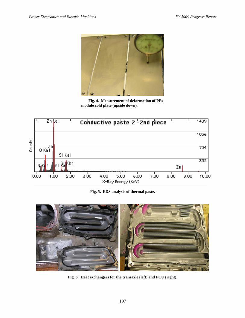
Power Electronics and Electric Machines FY 2009 Progress Report
107
Fig. 4. Measurement of deformation of PEs module cold plate (upside down).
Fig. 5. EDS analysis of thermal paste.
Fig. 6. Heat exchangers for the transaxle (left) and PCU (right).
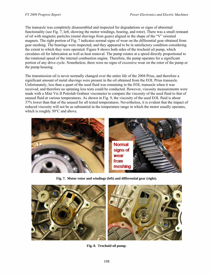
FY 2009 Progress Report Power Electronics and Electric Machines
108
The transaxle was completely disassembled and inspected for degradations or signs of abnormal functionality (see Fig. 7, left, showing the motor windings, bearing, and rotor). There was a small remnant of oil with magnetic particles (metal shavings from gears) aligned in the shape of the “V” oriented magnets. The right portion of Fig. 7 indicates normal signs of wear on the differential gear obtained from gear meshing. The bearings were inspected, and they appeared to be in satisfactory condition considering the extent to which they were operated. Figure 8 shows both sides of the trochoid oil pump, which circulates oil for lubrication as well as heat removal. The pump rotates at a speed directly proportional to the rotational speed of the internal combustion engine. Therefore, the pump operates for a significant portion of any drive cycle. Nonetheless, there were no signs of excessive wear on the rotor of the pump or the pump housing. The transmission oil is never normally changed over the entire life of the 2004 Prius, and therefore a significant amount of metal shavings were present in the oil obtained from the EOL Prius transaxle. Unfortunately, less than a quart of the used fluid was remaining in the EOL transaxle when it was received, and therefore no spinning loss tests could be conducted. However, viscosity measurements were made with a Mini Vis II Petrolab Grabner viscometer to compare the viscosity of the used fluid to that of unused fluid at various temperatures. As shown in Fig. 9, the viscosity of the used EOL fluid is about 37% lower than that of the unused for all tested temperatures. Nevertheless, it is evident that the impact of reduced viscosity will not be as substantial in the temperature range in which the motor usually operates, which is roughly 50°C and above.
Fig. 7. Motor rotor and windings (left) and differential gear (right).
Fig. 8. Trochoid oil pump.
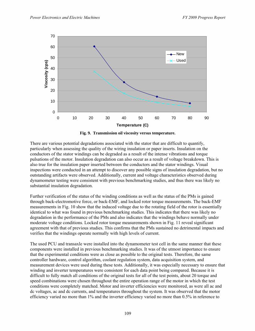
Power Electronics and Electric Machines FY 2009 Progress Report
109
0
10
20
30
40
50
60
70
0 10 20 30 40 50 60 70 80 90
Temperature (C)
Vis
cosi
ty (
cps)
New
Used
Fig. 9. Transmission oil viscosity versus temperature. There are various potential degradations associated with the stator that are difficult to quantify, particularly when assessing the quality of the wiring insulation or paper inserts. Insulation on the conductors of the stator windings can be degraded as a result of the intense vibrations and torque pulsations of the motor. Insulation degradation can also occur as a result of voltage breakdown. This is also true for the insulation paper inserted between the conductors and the stator windings. Visual inspections were conducted in an attempt to discover any possible signs of insulation degradation, but no outstanding artifacts were observed. Additionally, current and voltage characteristics observed during dynamometer testing were consistent with previous benchmarking studies, and thus there was likely no substantial insulation degradation. Further verification of the status of the winding conditions as well as the status of the PMs is gained through back-electromotive force, or back-EMF, and locked rotor torque measurements. The back-EMF measurements in Fig. 10 show that the induced voltage due to the rotating field of the rotor is essentially identical to what was found in previous benchmarking studies. This indicates that there was likely no degradation in the performance of the PMs and also indicates that the windings behave normally under moderate voltage conditions. Locked rotor torque measurements shown in Fig. 11 reveal significant agreement with that of previous studies. This confirms that the PMs sustained no detrimental impacts and verifies that the windings operate normally with high levels of current. The used PCU and transaxle were installed into the dynamometer test cell in the same manner that these components were installed in previous benchmarking studies. It was of the utmost importance to ensure that the experimental conditions were as close as possible to the original tests. Therefore, the same controller hardware, control algorithm, coolant regulation system, data acquisition system, and measurement devices were used during these tests. Additionally, it was especially necessary to ensure that winding and inverter temperatures were consistent for each data point being compared. Because it is difficult to fully match all conditions of the original tests for all of the test points, about 20 torque and speed combinations were chosen throughout the entire operation range of the motor in which the test conditions were completely matched. Motor and inverter efficiencies were monitored, as were all ac and dc voltages, ac and dc currents, and temperatures throughout the system. It was observed that the motor efficiency varied no more than 1% and the inverter efficiency varied no more than 0.5% in reference to
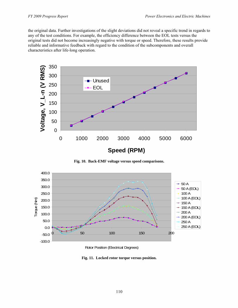
FY 2009 Progress Report Power Electronics and Electric Machines
110
the original data. Further investigations of the slight deviations did not reveal a specific trend in regards to any of the test conditions. For example, the efficiency difference between the EOL tests versus the original tests did not become increasingly negative with torque or speed. Therefore, these results provide reliable and informative feedback with regard to the condition of the subcomponents and overall characteristics after life-long operation.
0
50
100
150
200
250
300
350
0 1000 2000 3000 4000 5000 6000
Speed (RPM)
Vo
ltag
e, V
_L-n
(V
RM
S)
Unused
EOL
Fig. 10. Back-EMF voltage versus speed comparisons.
-100.0
-50.0
0.0
50.0
100.0
150.0
200.0
250.0
300.0
350.0
400.0
0 50 100 150 200
Rotor Position (Electrical Degrees)
Tor
que
(Nm
)
50 A50 A (EOL)100 A100 A (EOL)150 A150 A (EOL)200 A200 A (EOL)250 A250 A (EOL)
Fig. 11. Locked rotor torque versus position.
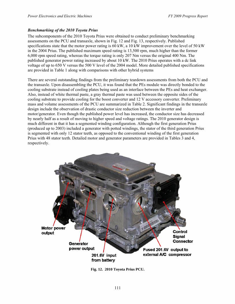
Power Electronics and Electric Machines FY 2009 Progress Report
111
Benchmarking of the 2010 Toyota Prius
The subcomponents of the 2010 Toyota Prius were obtained to conduct preliminary benchmarking assessments on the PCU and transaxle, shown in Fig. 12 and Fig. 13, respectively. Published specifications state that the motor power rating is 60 kW, a 10 kW improvement over the level of 50 kW in the 2004 Prius. The published maximum speed rating is 13,500 rpm, much higher than the former 6,000 rpm speed rating, whereas the torque rating is only 207 Nm versus the original 400 Nm. The published generator power rating increased by about 10 kW. The 2010 Prius operates with a dc link voltage of up to 650 V versus the 500 V level of the 2004 model. More detailed published specifications are provided in Table 1 along with comparisons with other hybrid systems There are several outstanding findings from the preliminary teardown assessments from both the PCU and the transaxle. Upon disassembling the PCU, it was found that the PEs module was directly bonded to the cooling substrate instead of cooling plates being used as an interface between the PEs and heat exchanger. Also, instead of white thermal paste, a gray thermal paste was used between the opposite sides of the cooling substrate to provide cooling for the boost converter and 12 V accessory converter. Preliminary mass and volume assessments of the PCU are summarized in Table 2. Significant findings in the transaxle design include the observation of drastic conductor size reduction between the inverter and motor/generator. Even though the published power level has increased, the conductor size has decreased by nearly half as a result of moving to higher speed and voltage ratings. The 2010 generator design is much different in that it has a segmented winding configuration. Although the first generation Prius (produced up to 2003) included a generator with potted windings, the stator of the third generation Prius is segmented with only 12 stator teeth, as opposed to the conventional winding of the first generation Prius with 48 stator teeth. Detailed motor and generator parameters are provided in Tables 3 and 4, respectively.
Fig. 12. 2010 Toyota Prius PCU.
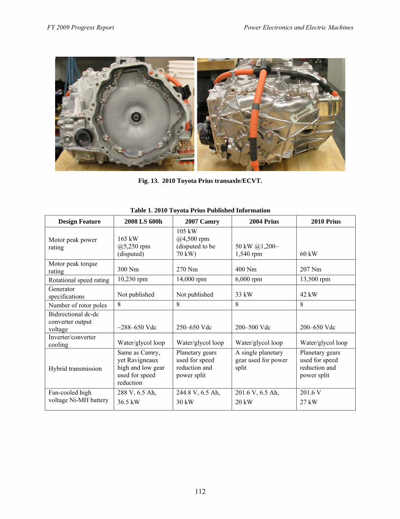
FY 2009 Progress Report Power Electronics and Electric Machines
112
Fig. 13. 2010 Toyota Prius transaxle/ECVT.
Table 1. 2010 Toyota Prius Published Information
Design Feature 2008 LS 600h 2007 Camry 2004 Prius 2010 Prius
Motor peak power rating
165 kW @5,250 rpm (disputed)
105 kW @4,500 rpm (disputed to be 70 kW)
50 kW @1,200–1,540 rpm 60 kW
Motor peak torque rating 300 Nm 270 Nm 400 Nm 207 Nm
Rotational speed rating 10,230 rpm 14,000 rpm 6,000 rpm 13,500 rpm
Generator specifications Not published Not published 33 kW 42 kW
Number of rotor poles 8 8 8 8
Bidirectional dc-dc converter output voltage ~288–650 Vdc 250–650 Vdc 200–500 Vdc 200–650 Vdc
Inverter/converter cooling Water/glycol loop Water/glycol loop Water/glycol loop Water/glycol loop
Hybrid transmission
Same as Camry, yet Ravigneaux high and low gear used for speed reduction
Planetary gears used for speed reduction and power split
A single planetary gear used for power split
Planetary gears used for speed reduction and power split
Fan-cooled high voltage Ni-MH battery
288 V, 6.5 Ah,
36.5 kW
244.8 V, 6.5 Ah,
30 kW
201.6 V, 6.5 Ah,
20 kW
201.6 V
27 kW
Power Electronics and Electric Machines FY 2009 Progress Report
113
Table 2. 2010 Toyota Prius PCU Preliminary Mass and Volume Assessments
Item Mass (kg) Volume (L)
Inverter/converter as received from original equipment manufacturers
13.0 ~18.6
PEs, controller/driver boards, cooling infrastructure 2.7 2.9 PEs, cooling infrastructure housing 1.9 3.6 Boost inductor, 12 V converter, and housing 5.9 5.8 Large capacitor 1.8 1.3 Connectors/sense wires/resistor 0.7 1.1
Table 3. 2010 Toyota Prius Motor Parameters
Parameter 2008 LS 600h
2007 Camry
2004 Prius
2010 Prius
Comments
Lamination dimensions
Stator outer diameter (OD) (cm) 20 26.4 26.9 26.4
Stator inner diameter (ID) (cm) 13.086 16.19 16.19 16.24
Stator stack length (cm) 13.54 6.07 8.4 5.08
Rotor OD (cm) 12.91 16.05 16.05 16.04
Rotor stack length (cm) 13.59 6.2 8.36 5.0165
Air gap (mm) 0.89 0.73025 0.73025 1.0033
Lamination thickness (mm) 0.28 0.31 0.33
Mass of assemblies
Rotor mass (kg) 11.93 9.03 10.2 6.7 Includes rotor shaft.
Stator mass (kg) 18.75 18 25.9 15.99
Stator wiring
Number of stator slots 48 48 48 48 Casing
Motor casing mass (kg) 14 9.5 8.9 15 Resolver, pump, etc
Table 4. 2010 Toyota Prius Generator Parameters
Parameter 2008 LS 600h
2007 Camry
2004 Prius
2010 Prius
Comments
Lamination dimensions
Stator OD (mm) 263.9 Same as LS
236.2 246.0
Stator ID (mm) 162.1 Same as LS
142.6 152.7
Stator stack length (cm) 7.07 3.58 3.05 2.7 Rotor OD (mm) 160.5 Same as
LS 140.72 151.3
Mass of assemblies
Rotor mass (kg) 9.7 5.19 4.01 3.93 Including rotor shaft Stator mass (kg) 20.5 12.09 9.16 8.58

FY 2009 Progress Report Power Electronics and Electric Machines
114
Conclusion • 2004 Prius EOL studies revealed only slight discrepancies.
— Measured motor efficiency changed no more than 1% from original tests. — Measured inverter efficiency changed no more than 0.5% from original tests. — Behavior of capacitors shows only miniscule differences. — No damage to stator windings was found. — Transmission oil, which impacts rotational losses, was found to have 40% lower viscosity for all
temperatures. — Slight wear due to gear meshing observed. — No degradation of PM capabilities over vehicle lifetime.
• Preliminary 2010 Toyota Prius benchmarking results were as follows.
— Motor speed rating has increased from 6,000 rpm to 13,500 rpm. — Maximum boosted dc voltage has increased from 500 V to 650 V. — Size of motor/generator power leads has been drastically reduced. — PEs module is bonded directly to the water-cooled heat exchanger. — Preliminary mass and volume assessments indicate significant reduction in motor size.
Publications None. References None. Patents None.

Power Electronics and Electric Machines FY 2009 Progress Report
DISTRIBUTION
Internal 1. D. J. Adams 2. K. P. Gambrell 3. J. B. Green, Jr. 4. L. D. Marlino
5. M. Olszewski 6. Laboratory Records Authors Coauthors
External 7. R. Al-Attar, DCX, [email protected]. 8. S. J. Boyd, U.S. Department of Energy, EE-2G/Forrestal Building, 1000 Independence Avenue,
S.W., Washington, D.C. 20585. 9. J. Czubay, General Motors Corporation, GM Powertrain Headquarters, Mail Code: 483-710-270,
895 Joslyn Avenue, Pontiac, Michigan 48340. 10. H. Dadkhah, Chrysler, LLC, CIMS 526-00-00, 1960 Technology Drive, Building D, Troy,
Michigan 48083. 11. P. B. Davis, U.S. Department of Energy, EE-2G/Forrestal Building, 1000 Independence Avenue,
S.W., Washington, D.C. 20585. 12. R. R. Fessler, BIZTEK Consulting, Inc., 820 Roslyn Place, Evanston, Illinois 60201-1724. 13. S. Gopalakrishnan, General Motors Corporation, RMB-356, Mail Code 480-106-390, 30500
Mound Road, Warren, Michigan 48090. 14. G. Hagey, 501 Randolph St., Williamsburg, Virginia 23185. 15. E. Jih, Ford Motor Company, Scientific Research Laboratory, 2101 Village Road, MD-1170, Rm.
2331, Dearborn, Michigan 48121. 16. K. J. Kelly, National Renewable Energy Laboratory, 1617 Cole Boulevard, Golden, Colorado
80401. 17. F. Leonardi, Ford Motor Company, 15050 Commerce Drive, North, Dearborn, Michigan
48120-1261. 18. F. Liang, Ford Motor Company, Scientific Research Laboratory, 2101 Village Road, MD1170,
Rm. 2331/SRL, Dearborn, Michigan 48121. 19. M. W. Lloyd, Energetics, Inc., 7164 Columbia Gateway Drive, Columbia, Maryland 21046. 20. M. Mehall, Ford Motor Company, Scientific Research Laboratory, 2101 Village Road, MD-2247,
Rm. 3317, Dearborn, Michigan 48124-2053. 21. N. Olds, United States Council for Automotive Research (USCAR), [email protected]. 22. S. A. Rogers, U.S. Department of Energy, EE-2G/Forrestal Building, 1000 Independence Avenue,
S.W., Washington, D.C. 20585. 23. G. S. Smith, General Motors Advanced Technology Center, 3050 Lomita Boulevard, Torrance,
California 90505.