Embed Size (px)
Citation preview

ToF AFE
(OPT3101)
Cliff Detection
Stuck
Prevention
Obstacle
Detection
Depth Data
3.3 V
MCU
(MSP430)
LDO
(TPS73633)
3.3 V
5 V
1TIDUET2–September 2019Submit Documentation Feedback
Copyright © 2019, Texas Instruments Incorporated
Obstacle, Cliff Detection and Stuck Prevention All-In-One Reference Designfor Robotic Applications
Design Guide: TIDA-010077Obstacle, Cliff Detection and Stuck Prevention All-In-OneReference Design for Robotic Applications
DescriptionObstacle avoidance, cliff detection, stuck prevention,and wall follow are key features for robotic systems.This reference design uses optical time-of-flight (ToF)techniques to build small and cost-effective proximitysensor systems to achieve these features. with asingle proximity and distance sensor analog front end(AFE) (OPT3101) with three external near-infrared(NIR) LEDs, and one photodiode.
Resources
TIDA-010077 Design FolderOPT3101 Product FolderLM2664 Product FolderMSP430FR2476 Product FolderTLC59283 Product FolderTLV702 Product FolderTPD2E001 Product Folder
Search Our E2E™ support forums
Features• Three NIR emitters can be configured for different
functions: Cliff detection, obstacle avoidance, stuckprevention, and wall follow
• Detection range up to 1.5 meters without a lens forobstacle avoidance
• Adaptive high dynamic range (HDR) enables thedetection range to be short enough for cliffdetection and stuck prevention
• ToF-based sensing AFE (OPT3101) makesmeasurement insensitive to object color andreflectivity and supports operation under highambient condition (outdoor conditions)
• Direct distance measurement output with anaccuracy of ±5%
• Low-power mode running at 1 sample per secondwith a power drain of 30 mW
Applications• Vacuum robot• Robotic lawn mower• Other robot
An IMPORTANT NOTICE at the end of this TI reference design addresses authorized use, intellectual property matters and otherimportant disclaimers and information.

System Description www.ti.com
2 TIDUET2–September 2019Submit Documentation Feedback
Copyright © 2019, Texas Instruments Incorporated
Obstacle, Cliff Detection and Stuck Prevention All-In-One Reference Designfor Robotic Applications
1 System DescriptionWith the rapid development of household and industrial robots, highly-reliable proximity sensing isbecoming an important feature and capability. A robot is often required to sense any objects in front of it tomake responses. For instance, a robotic should have the capability to sense obstacles and to avoid acollision. It also needs to sense any cliff ahead to avoid dropping or any object above it to avoid beingtrapped. One of the most common challenges for obstacle sensing is that the traditional sensor can easilyget affected by temperature, object color, and ambient light, causing large detection error or even falsetriggering. Another common design challenge is that traditional sensor can only sense the object inhorizontal plane, which may cause the robot to become in certain conditions, for example under the bed.ToF technology is the suitable solution to solve these issues.
The purpose of the TIDA-010077 reference design is to demonstrate the 1D ToF capabilities of TI'sOPT3101 device to solve the previously-mentioned design challenges in different application scenarios forrobotics. This reference design includes two boards: the sensor board and the display board. The sensorboard is an optical ToF proximity and distance sensing module, consisting of the OPT3101 AFE and itsperipheral device. Three LEDs and one photodiode are connected to the OPT3101 as illuminators andreceiver. All the computation and corrections for crosstalk, phase offset, temperature-dependent phasedrift, and ambient-dependent phase drift are done on the OPT3101 device. The display module uses anexternal MCU (MSP430FR2476RGER) to control the OPT3101 AFE and an external EEPROM to storecalibration data, and then display the distance information of the target to the user through a seven-segment LED display (LTD-6910HR) after reading the data from the sensor module. The MCU directlyreads out the depth data through an I2C interface from the sensing module. The MCU can also be used forfactory calibration purposes.
Comparing to the other detection and ranging approaches such as ultrasonic and radar technologies, withweaknesses, such as accuracy and ambient immunity, TI’s OPT3101 device, a long-range proximity anddistance sensor Analog-Front-End (AFE), uses the Time-of-Flight (ToF) principle to acquire distancemeasurement data with well performance of distance, and accuracy under different ambient conditions.
The typical advantages of TI’s OPT3101 AFE are as follows:• Flexibility: The OPT3101 device offers the flexibility to customize a design for specific applications. It
has a built in illumination driver, supporting up to three separate illumination channels activated in turn,with separate current control programmability. Additionally, with different types of external illuminators(LED, VCSEL, or LASER) and corresponding photodiodes, users have the choice of a widewavelength of interest (visible or infrared) and field of view (FoV) based on added optics. This helpsoptimize the design both in terms of build of materials (BOM) and size to get the best end result.
• High speed and high resolution: The OPT3101 device has the sample rate up to 4 kHz, with ToFtechnology, operating much faster compared to other range-sensing methods like ultrasonic sensing.The OPT3101 device has 16-bit distance output at 15-m unambiguous range. In addition, TI’sadvanced ToF technology deploys multi-frequency techniques for de-aliasing to extend the distancerange.
• Object reflectivity independency: The ToF technology independently determines phase andamplitude, allowing for independency of object (color) reflectivity. It overcomes the drawback of anamplitude based system, which estimates distance only based on the reflected signal strength.
• High ambient rejection ratio: The OPT3101 device has excellent ambient and sunlight rejectionperformance. There exists an internal ambient cancellation block in the OPT3101 device that allows forgreat performance both indoors and outdoors, including full sunlight of 130 klx. The OPT3101 devicealso has other various calibrations and compensation approaches, ranging from crosstalk, phaseoffset, phase correction with temperature and ambient, and so forth, that ensures higher accuracy.
• Adaptive HDR: The timing sequencer is highly configurable to provide for application-specific trade-offs of power versus performance, ranging from µW to mW of power based on data and accuracy.

www.ti.com System Description
3TIDUET2–September 2019Submit Documentation Feedback
Copyright © 2019, Texas Instruments Incorporated
Obstacle, Cliff Detection and Stuck Prevention All-In-One Reference Designfor Robotic Applications
Adaptive HDR allows the sequencer switching between high and low illumination driver currents toextend the dynamic range, depending on the signal saturation and lower amplitude threshold, as wellas save power.
1.1 Key System Specifications
Table 1. Key System Specifications
PARAMETER MIN NOM MAX UNIT CommentsDC input power supply 3.6 5 5.5 VDC DC input by J4 (display board USB)Sensor power supply 3 3.3 3.6 VDC Sensor board J1
Detection range (Channel 1) 0.05 — 1.5 m Obstacle detection without lens forall color target
Detection range (Channel 0, 2) 0.01 — 0.5 m Cliff detection, stuck prevention, andwall follow
Field of View (FOV for Channel 0) –5 — 5 degree Cliff detectionField of View (FOV for Channel 1) –20 — 20 degree Obstacle detectionField of View (FOV for Channel 2) –3 — 3 degree Stuck prevention, wall follow
Continuous full power — — 300 mW
Sensor board only, continuousmeasuring distance at 128 subframes per sample and 31.25
samples per secondAccuracy — — 5 %
Low-power mode — — 30 mW Wake up every 1 s for one sample(128 sub frames)
Operating temperature –20 — 60 °C

ToF AFE
(OPT3101)
Cliff Detection
Stuck
Prevention
Obstacle
Detection
Depth Data
3.3 V
MCU
(MSP430)
LDO
(TPS73633)
3.3 V
5 V
System Overview www.ti.com
4 TIDUET2–September 2019Submit Documentation Feedback
Copyright © 2019, Texas Instruments Incorporated
Obstacle, Cliff Detection and Stuck Prevention All-In-One Reference Designfor Robotic Applications
2 System Overview
2.1 Block Diagram
Figure 1. TIDA-010077 Block Diagram
2.2 Design ConsiderationsThis reference design is based on the OPT3101 (TI 1D ToF AFE) to realize cliff detection, obstacleavoidance, and stuck prevention functions in one miniature module. It can also be used for wall follow.
The OPT3101 device supports up to three transmitter channels for multi-zone operation. Based on thisfeature, one OPT3101 device can be used for multi-functions. Different functions have differentrequirements and the OPT3101 AFE is flexible enough to customize a design with a wide variety ofphotodiodes and emitters. For example, obstacle detection requires a wide field-of-view and longerdetection range so an emitter with a wide FoV is needed when cliff detection needs a narrow FoV andshort distance detection capability. See Section 2.4 for details.
2.3 Highlighted ProductsThe following subsections detail the highlighted products used in this reference design, including the keyfeatures for their selection. See their respective product data sheets for the complete details on anyhighlighted device.
2.3.1 OPT3101The OPT3101 device is a high-speed, high-resolution and fully-integrated analog front end (AFE) forcontinuous-wave, time-of-flight (ToF) based proximity sensing and range finding using active illumination.The OPT3101 AFE connects to an external illuminator (LED, VCSEL, or LASER) to transmit modulatedoptical signals, and reflected signals are received by an external photodiode which connects to the input ofthe AFE. The received signal is converted to amplitude and phase information by the AFE and depthengine. This output is stored in registers, which can be read out through the device I2C interface.

ToF
Receiver
Ambient
CancellationAmb
ADC
Depth
Engine
Timing
Gen
CLK
GEN
REGISTERSREGISTERS
I2C
Slave
Illumination Driver
SDA_S
SCL_S
GP1
GP2
Osc
Temp
Sensor
Temp_DigI2C
Master
SDA_M SCL_M
TX2 TX1 VSS TX0
INP
INM
ReF CLK IN
INT Out
Data Ready
I
Q
10 MHz
www.ti.com System Overview
5TIDUET2–September 2019Submit Documentation Feedback
Copyright © 2019, Texas Instruments Incorporated
Obstacle, Cliff Detection and Stuck Prevention All-In-One Reference Designfor Robotic Applications
The device integrates the complete depth processing pipeline that includes the ADC, timing sequencer,and the digital processing engine. The device also has a built-in illumination driver that covers most of thetarget applications. Given the high ambient rejection ratio, the device can support very high ambientconditions, including full sunlight of 130 klx. The timing sequencer is highly configurable to provide forapplication-specific trade-offs of power versus performance. The device provides depth data that consistsof phase, amplitude, and ambient measurements. The calibration subsystem supports phase-datacalibration for inaccuracies resulting from temperature and crosstalk.
Figure 2. OPT3101 Block Diagram
2.3.2 MSP430FR2476The MSP430FR2476 microcontroller (MCU) is part of the MSP430™ value line sensing portfolio, TI'slowest-cost family of MCUs for sensing and measurement applications. The architecture, ferroelectricRAM (FRAM), and integrated peripherals, combined with extensive low-power modes, are optimized toachieve extended battery life in portable and battery-powered sensing applications in a small VQFNpackage (4 mm × 4 mm).
TI's MSP430 ultra-low-power FRAM microcontroller platform combines uniquely embedded FRAM and aholistic ultra-low-power system architecture, allowing system designers to increase performance whilelowering energy consumption. FRAM technology combines the low-energy fast writes, flexibility, andendurance of RAM with the non-volatility of flash.
Figure 3 shows the functional block diagram.

SYS
Watchdog
CRC16
16-bit cyclic
Redundancy
check
MPY32
32-bit
Hardware
multiplier
4xTA3
Timer_A3
3 CC
registers
2xeUSCI_A
UART,
IrDA, SPI
2xeUSCI_B
SPI, I2C
1xTB7
Timer_B7
7 CC
registers
RTC
16-bit
real-time
clock
BAKMEM
32-byte
backup
memory
LFXT
Clock
System
FRAM
64KB+512B
32KB+512B
RAM
8KB
4KB
ADC
12 bit, up to
12 channels,
single-ended
I/O Ports
P1, P2
2x8 IOs
PA
1x16 IOs
eCOMP
Enhanced
comparator
With 6-bit
DAC
I/O PortsP3, P4
2x8 IOs
PB
1x16 IOs
I/O PortsP5, P6
1x8 Ios
1x3 IOs
PB
1x16 IOs
LPM3.5 Domain
16-MHz CPU
With
16 registers
Power
Management
Module
EEM
JTAG
SBW
MAB
MDB
DVCC
DVSS
RST/NMI
XIN XOUT
TCK
TMS
TDI/TCLK
TDO
SBWTCK
SBWTDIO
P1.x/P2.x P3.x/P4.x P5.x/P6.x
System Overview www.ti.com
6 TIDUET2–September 2019Submit Documentation Feedback
Copyright © 2019, Texas Instruments Incorporated
Obstacle, Cliff Detection and Stuck Prevention All-In-One Reference Designfor Robotic Applications
Figure 3. MSP430FR2476 Block Diagram
2.3.3 TLC59283The TLC59283 is a 16-channel, constant-current sink light-emitting diode (LED) driver. Each channel canbe individually controlled with a simple serial communications protocol that is compatible with 3.3-V or 5-VCMOS logic levels, depending on the operating VCC. When the serial data buffer is loaded, a LAT risingedge transfers the data to the OUTn outputs. The BLANK pin can be used to turn off all OUTn outputsduring power-on and output data latching to prevent unwanted image displays during these times. Theconstant-current value of all 16 channels is set by a single external resistor. Each constant-current outputhas a pre-charge field-effect transistor (FET) that can reduce ghosting on the multiplexing (dynamic) driveLED display. Multiple TLC59283s can be cascaded together to control additional LEDs from the sameprocessor.
Figure 4 shows the functional block diagram.

16-Bit Shift Register
(1 Bit × 16 Channels)
Output On or Off Data Latch
(1 Bit × 16 Channels)
16-Channel Constant-Current Sink Driver
With Grouped Switching Delay
Timing
Control
Pre-Charge
FETs
VCC - 1.4 V
(typ)
ALLOFF
15
MSB
15
MSB
SOUT
OUT0 OUT1 OUT14 OUT15
GND
0
LSB
0
LSB
VCC
VCC
SIN
SCLK
LAT
BLANK
IREF
GND
www.ti.com System Overview
7TIDUET2–September 2019Submit Documentation Feedback
Copyright © 2019, Texas Instruments Incorporated
Obstacle, Cliff Detection and Stuck Prevention All-In-One Reference Designfor Robotic Applications
Figure 4. TLC59283 Block Diagram
2.3.4 LM2664The LM2664 CMOS charge-pump voltage converter inverts a positive voltage in the range of 1.8 V to 5.5V to the corresponding negative voltage of −1.8 V to −5.5 V. The device uses two low-cost capacitors toprovide up to 40 mA of output current.
The LM2664 operates at 160-kHz oscillator frequency to reduce output resistance and voltage ripple. Withan operating current of only 220 µA (operating efficiency greater than 91% with most loads) and 1-µAtypical shutdown current, the LM2664 provides ideal performance for battery-powered systems.
2.3.5 TLV70233The TLV702 series of low-dropout (LDO) linear regulators are low quiescent current devices with excellentline and load transient performance. These LDOs are designed for power-sensitive applications. Aprecision band-gap and error amplifier provides overall 2% accuracy. Low output noise, very high power-supply rejection ratio (PSRR), and low dropout voltage make this series of devices ideal for most battery-operated handheld equipment. All device versions have integrated thermal shutdown, current limit, andundervoltage lockout (UVLO).
System Overview www.ti.com
8 TIDUET2–September 2019Submit Documentation Feedback
Copyright © 2019, Texas Instruments Incorporated
Obstacle, Cliff Detection and Stuck Prevention All-In-One Reference Designfor Robotic Applications
2.3.6 TPD2E001The TPD2E001 device is a two-channel transient voltage suppressor (TVS) based ESD protection diodearray. The TPD2E001 device is rated to dissipate ESD strikes at the maximum level specified in the IEC61000-4-2 Level 4 international standard.
2.4 System Design TheoryThe block diagram in Figure 1 shows that the complete system is composed of two main sections: aminiature optical ToF sensor module with direct distance data output and a display module which is usedto control the sensor module and show the distance information measured by the sensor module to user.
2.4.1 Sensor Module DesignThe sensor module design aims to achieve the obstacle avoidance, cliff detection, stuck prevention, andwall follow functions. Figure 5 shows an example of a typical system definition.
Figure 5. Sensor Key Functions in Robot
2.4.1.1 System Design Goal ParametersTable 2 elucidates the design goal parameters for this reference design. These parameters are used infurther calculations to select components.
Table 2. Application Requirement Specifications
SPECIFICATION VALUE UNITS COMMENTS
Channel 0
Maximum distance 0.5 m For an object with 20% to approximately 80% reflectivityMinimum distance 0.01 m For an object with 20% to approximately 80% reflectivityDistance accuracy 10 % For an object with 20% reflectivity at 0.5 meters worst.
Field of View ≤ ±5 degrees ≤ 10° for full angle
Channel 1
Maximum distance 1.5 m For an object with 2080% reflectivityMinimum distance 0.05 m For an object with 20% to approximately 80% reflectivityDistance accuracy 10 % For an object with 20% reflectivity at 1.5 meters worst.
Field of View ±20 degrees 40° for full angle
Channel 2
Maximum distance 0.5 m For an object with 20% to approximately 80% reflectivityMinimum distance 0.01 m For an object with 20% to approximately 80% reflectivityDistance accuracy 10 % For an object with 20% reflectivity at 0.5 meters worst.
Field of View ≤ ±5 degrees ≤ 10° for full angle
AllAmbient light 130 klx Sunlight conditionSamples rate 10 SPS For each channel

Emitter FoV
halfAngle
Emitter
Receiver FoVhalfAngleReceiver
TARGET
www.ti.com System Overview
9TIDUET2–September 2019Submit Documentation Feedback
Copyright © 2019, Texas Instruments Incorporated
Obstacle, Cliff Detection and Stuck Prevention All-In-One Reference Designfor Robotic Applications
2.4.1.2 Target TypeBased on the reflectance of objects, the target can be classified as diffused reflector, shiny reflector, andretroreflector. For a detailed description of these three target type, see the Introduction to Time-of-FlightLong Range Proximity and Distance Sensor System Design User's Guide for more information.
In this reference design, the sensor detects the objects in the sensing area. Target objects are oftendiffused reflectors. The reflectivity of the target expressed in ratio % is characterized by the ratio of thetotal amount of light reflected off the surface to the ratio of the light incident on the surface. White paperhas a reflectivity of over 90% and black denim cloth has a reflectivity of approximately 10%. These aremuch easier to deal with since the light cast on the target is evenly distributed in all directions making thesystem immune to the angle and position in which the target lies.
2.4.1.3 Number of ChannelsThe OPT3101 device supports up to 3 transmitter channels. In other words, three channels can bemeasured simultaneously with one single OPT3101 device to realize different functions, such as cliffdetection, obstacle detection, stuck prevention, and wall follow. All these functions can be realized withone miniature sensor module.
2.4.1.4 Field-of-View (FoV)Figure 6 shows the definition of FoV. The performance of the system is a strong function of the FoV sincemany parameters are dependent on it. Generally, the narrower the FoV, the longer the range of thesystem. There are 2 fields-of-view to be considered, the FoV of the emitter and the FoV of the receiver.
Figure 6. Emitter and Receiver Fields-of-View
2.4.1.4.1 Emitter FoVThe FOV of emitter is often measured in degrees and expressed in half-angle or full-angle subtended bythe cone of light emission. The selection of the emitter FoV is application specific. Ranging applicationsdemand extremely low emitter FoV whereas object or presence detection demands a large emitter FoV.Minimizing the FoV as small as possible (to a bare minimum, based on application requirement) helpsimprove the performance and range of the system.
In this design, the emitter FOV for obstacle detection should be no less than 40°. The emitter FoV for cliffdetection, stuck prevention, and wall follow can be less than 10°, for example ±5°, ±3°.

2
2
1signaGain
fovtan
2
fovambientGain tan
2
v§ ·§ ·¨ ¸¨ ¸
© ¹© ¹
§ ·§ ·v ¨ ¸¨ ¸
© ¹© ¹
System Overview www.ti.com
10 TIDUET2–September 2019Submit Documentation Feedback
Copyright © 2019, Texas Instruments Incorporated
Obstacle, Cliff Detection and Stuck Prevention All-In-One Reference Designfor Robotic Applications
2.4.1.4.2 FoV of ReceiverSimilarly, the FoV of the receiver which is usually a photodiode can be expressed in half-angle or fullangle, subtended by the cone of light collection and measured in degrees. The OPT3101 device can onlyaccept one receiver to receive the reflection of light. Therefore, the FoV of the receiver needs to be equalto or larger than the system FoV which is defined as 120°. But it is not the case that the larger, the better.Performance is a strong function of FoV and it has a great impact on both ambient light collection andsignal light collection. First-order approximation for the respective gains are found using Equation 1. Thisshows that reducing the FoV increases both signal gain and reduces ambient gain improving performanceby a great deal.
(1)
Therefore, a FoV of receiver range from 120° to 130° is the best choice.
2.4.1.5 Wavelength (λ)
2.4.1.5.1 Medium of TransmissionIn the application of proximity sensing for major appliances, the transmission medium is air, where theproperties of transmission are the same in the wavelengths of consideration. Sometimes the sensor needsto fixed behind some kind of glass or plastic panel which shields the visibility of the sensor module fromexternal influences. In this case, it is necessary to ensure that the material of the panel has goodpenetration to the light of the selected wavelength.
2.4.1.5.2 Eye and Skin SafetyEye and skin safety standards are very dependent on the wavelength of operation. Based on the chosenwavelength, different aspects of safety measurements and safety analysis must be made to certify andclassify the system. There are different lists of compliance checks and measurements based on thewavelength chosen both for laser or VCSEL sources and LEDs. Hence, while choosing center wavelengththese parameters must be considered as well.
2.4.1.5.3 Visibility to Naked EyeVisibility to the naked eye of a light source which is used as an emitter depends on the applicationrequirements. The OPT3101 device being just an AFE, supports a wide variety of wavelengths subjectedonly to the availability of photodiode and emitter components. The emitter and photodiode should havematching peak sensitivities.
Emitters usually have two categories based on visibility to the naked eye: visible spectrum and invisiblespectrum. The visible light wavelength ranges from 390 nm to 700 nm and the response of the human eyepeaks around 500 nm to 550 nm. In ToF-based systems, a near-infrared wavelength ranging from 750 nmto 1400 nm is in the invisible spectrum and widely adopted. Since NIR wavelengths are very close to thevisible range, NIR emitters are still visible to the naked eye under dark enough circumstances. This ispredominant with emitters around 850 nm. This may be unacceptable in certain applications where usersare distracted. In such cases going deeper into the NIR spectrum helps, like moving to 940 nm.
The proximity sensing in major appliances often require no visible detection wavelength. The spectrum ofthe emitter should be in the NIR field and the wavelength (λ in nm) of light illuminating by emitter shouldbe no less than 850 nm.

www.ti.com System Overview
11TIDUET2–September 2019Submit Documentation Feedback
Copyright © 2019, Texas Instruments Incorporated
Obstacle, Cliff Detection and Stuck Prevention All-In-One Reference Designfor Robotic Applications
2.4.1.6 Target DistanceThe performance of the system is a strong function of the target distance. OPT3101-based systems arecapable of operating over a wide range of target distances (from a few mm to tens of meters) based oncomponent selection and optics design. In this design of application, the target distance in this applicationis different for three channels. Obstacle detection channel 1 ranges from 0.05 to 1.5 meters with 10%accuracy of distance output, while channel 0 and 2 for cliff detection, stuck prevention, or wall followranges from 0.01 to 0.5 meters.
2.4.1.7 Dynamic RangeIn ToF-based applications, the strength of reflected light determines the dynamic range. The photodiodemay enter saturation status when reflected light is too strong such as short distance measurement. But forlong distance measurement, the strength of reflected light may be too weak for the OPT3101 device tooperate reliably. So dynamic range is represented by the range of operating conditions for which theOPT3101-based system is expected to operate without losing performance target and saturation. Theadaptive HDR of the OPT3101 device can be set to increase the dynamic range.• Distance range:
System is expected to work from 50 mm to 1500 mm for channel 1, then the dynamic range required is900 times or 59 dB (follows the square law for distance)System is expected to work from 10 mm to 500 mm for channel 0 and 2, then the dynamic rangerequired is 2500 times or 68 dB (follows the square law for distance)
• Reflectivity range:System is expected to work for both 10% reflectivity target and 90% reflectivity target, then thedynamic range required is 9 times or 19 dB
The dynamic range requirement for channel 1 is 900 × 9 = 8100 (expressed in ratio of maximum tominimum) or when expressed in decibels – it is 78 dB.
The other two channels is 2500 × 9 = 22500 (expressed in ratio of maximum to minimum) or whenexpressed in decibels – it is 87 dB.
2.4.1.8 Data RateThe data rate is typically specified as a system vector input for the design based on application need. Inthis design, the data rate for proximity sensing is defined to run at 10 samples per second (SPS). Sincethe system FoV of 120° in this design is covered by three emitters, the total samples per second for theOPT3101 device is 30.
2.4.1.9 Selection of Emitter
2.4.1.9.1 Type of IlluminatorThe OPT3101 device is a fully integrated analog front end (AFE) based on the time-of-flight (ToF) principleusing active illumination. The OPT3101 AFE connects to an external illuminator (LED, VCSEL, or LASER)to transmit modulated optical signals, and reflected signals are received by an external photodiode whichconnects to the input of the AFE. The received signal is converted to amplitude and phase information bythe AFE and depth engine.
LEDs are the most common and least expensive type of illuminator. LEDs are available in a wide range ofwavelengths, power levels, and FoVs. LEDs tend to have lower efficiency due to light extraction loss andpoor heat dissipation as compared to other illuminators. Since the light coming from the LED is notcoherent and from a large surface area, these are extremely hard to collimate to a narrow beam.However, for application requirements larger than around a ±3° of FoV, LEDs are suitable. LEDs haverobust construction, hence, have a better ESD performance and failure rate, and are therefore preferredfor automotive applications compared to the other types of emitters. Depending on the power of theemitter, FoV LED certification and lamp source classification may be required.

System Overview www.ti.com
12 TIDUET2–September 2019Submit Documentation Feedback
Copyright © 2019, Texas Instruments Incorporated
Obstacle, Cliff Detection and Stuck Prevention All-In-One Reference Designfor Robotic Applications
Edge-Lasers are available for specific wavelengths and power levels from selected distributors. These aremore expensive compared to LEDs, but have higher efficiencies. The light generated is coherent, from asmall apparent source; therefore, can be collimated to a very high degree. For example, a laser sourcewith a collimating lens can be focused to a beam as narrow as a few mm in diameter, maintaining itsbeam diameter to a distance up to several meters. However, high-power lasers could be harmful and haveexport control regulations and require additional certification. These emitters are very sensitive to ESD andovervoltage damage. Adding protection circuitry in the illumination circuitry extends system longevity.
VCSELs are similar to lasers, except their construction allows them to be highly-efficient emitters availableat various different power levels. Sometimes VCSELs are custom made as per required specifications.Due to their physical construction, VCSELs have the highest-efficiency emitters available in the smallestform-factor packages. VCSEL light is coherent and may be collimated to a great degree, similar to edgeemitting lasers. VCSEL packages can also be designed to have specific diffusers as part of the packageto achieve required intensity profiles. However, high-power VCSELs could be harmful to the naked eye;therefore, they have export control regulations and need additional certification. These emitters are verysensitive to ESD and overvoltage damage. Adding protection circuitry in the illumination circuitry helpssystem longevity.
For applications like cliff detection, obstacle detection, stuck prevention, and wall follow, high-powerInfrared LED is the best choice. The evaluation of eye safety occurs according to the standard IEC62471:2006 (photo biological safety of lamps and lamp systems). Within the risk grouping system of thisIEC standard, the LED falling into the class exempt group can be selected in this application.
2.4.1.9.2 Emitter Specification ParametersTable 3 shows the parameters requirement for high-power infrared LED selection based on previousdiscussion.
Table 3. Emitter Specification Parameters
PARAMETERS VALUE UNIT COMMENTSFoV (Full-Angle) 40–50 degree ±20° – ±25° (Half-Angle) for obstacle detectionFoV (Full-Angle) < 10 degree Cliff detection, stuck prevention, and wall follow
Wavelength ≥ 850 nm
Eye safety exempt group – Standard IEC 62471:2006 (photo-biological safety oflamps and lamp systems)
2.4.1.9.3 Selection ResultThree different types of infrared LED are chosen in this design for specific functions. Table 4 shows thebrief parameters for these LEDs. Download the data sheet for these LEDs by clicking the part number inthe following table.
Table 4. Emitter Specification Parameters
SPECIFICATION SFH 4550 SFH 4555 SFH 4556Peak wavelength (nm) 860 860 860
Centroid wavelength (nm) 850 850 850Spectral bandwidth at 50% Irel,max (nm) 30 30 30
Half angle (degree) 3 5 20Rise time (10%, 90%) IF = 100 mA; RL = 50 Ω (ns) 12 12 12Fall time (10%, 90%) IF = 100 mA; RL = 50 Ω (ns) 12 12 12

www.ti.com System Overview
13TIDUET2–September 2019Submit Documentation Feedback
Copyright © 2019, Texas Instruments Incorporated
Obstacle, Cliff Detection and Stuck Prevention All-In-One Reference Designfor Robotic Applications
2.4.1.10 Photodiode Selection
2.4.1.10.1 Type of PhotodiodePIN photodiodes are recommended due to their responsitivity and fast switching times. Photodiodesfundamentally respond to a large bandwidth of wavelengths (spectral bandwidth); however, they havepeak sensitivity only at a particular wavelength. The photodiode should also have peak sensitivitymatching the peak spectral emission of the LED.
2.4.1.10.2 Wavelength (λ in nm)Photodiodes fundamentally respond to a large bandwidth of wavelengths (spectral bandwidth); however,they have peak sensitivity only at a particular wavelength. Photodiodes are best operated at thatwavelength to reap the best performance, although this is not a strict requirement. The wider the spectralbandwidth of the photodiode, the more current it generates from sunlight or other ambient light posing alimitation to the system, hence, a photodiode with a built-in filter around the wavelength of interest helpsimprove ambient performance. In Section 2.4.1.9.3, the centroid wavelength of emitter is 850 nm. So thewavelength of peak sensitivity for the photodiode should be around 850 nm.
2.4.1.10.3 Junction Capacitance (Cj in pF)In an OPT3101 system, the photodiode is reverse-biased at a constant 1 V. Hence, the junctioncapacitance of the photodiode when reversed-biased at 1 V, determines the performance of the system.The OPT3101 device supports a maximum capacitance of 6 pF. So the junction capacitance of thephotodiode at 1-V bias should be less than 6 pF. Negative voltage to photodiode help to reduce thecrosstalk. As is described in Section 2.4.1.11, -3.3-V is connected to photodiode In this design.
2.4.1.10.4 Rise and Fall TimesThe OPT3101 device operates at 10 MHz, hence photodiodes with rise and fall times ≤ 10 ns arerecommended. Choosing photodiodes with larger rise and fall times could mean a loss in performance.
2.4.1.10.5 Package and Case Type SelectionPhotodiodes come in various different packages and cases with different soldering options. SMDcomponents tend to have profile height; therefore, better parasitic and crosstalk resilience. In this design,the application requires a 120° FoV that is covered by three emitters; therefore, through-hole photodiodesare chosen so that they can be bent to the right direction.
2.4.1.10.6 Photodiode Selection ParametersTable 5 shows the parameter requirements for photodiode selection, based on the previous discussion.
Table 5. Photodiode Selection Parameters
FoV TYPE WAVELENGTH JUNCTIONCAPACITANCE RISE AND FALL TIMES PACKAGE
≥ 120° PIN Near 850 nm < 6 pF at 1 V ≤ 10 ns TH
2.4.1.10.7 Photodiode Selection ResultThe OSRAM SFH203PFA photodiode meets the required parameters. Figure 7 and Figure 8 show thephotodiode characteristics. Table 6 lists the photodiode specifications.

O (nm) o
Sre
l (%
) o
400 600 800 1000 12000
20
40
60
80
100
D024VR (V)
C0 (
pF
)
0.01 0.1 1 10 1002
3
4
5
6
7
8
9
10
11
12
D023
System Overview www.ti.com
14 TIDUET2–September 2019Submit Documentation Feedback
Copyright © 2019, Texas Instruments Incorporated
Obstacle, Cliff Detection and Stuck Prevention All-In-One Reference Designfor Robotic Applications
Figure 7. SFH203PFA Relative Spectral Sensitivity Figure 8. SFH203PFA Photodiode Reverse Bias Capacitance
See the Directional Characteristics graph in the SFH 203 PFA Data Sheet from Osram OptoSemiconductors.
Table 6. Emitter Specification Parameters
SPECIFICATION VALUE UNITS COMMENTSPhotodiode current with 1 mW/cm2 6.2 µA Photodiode specification
Half-angle ±75 degree Photodiode specificationAmbient current 105 µA See the OPT3101 system estimator tool
Reverse bias capacitance at VR = 1 V 5.8 pF AFE supports a maximum capacitance of 6 pFReverse bias capacitance at VR = 4.3 V 3.6 pF -3.3V connected to photodiode
Use the OPT3101 System Estimator Software for system performance estimation.
2.4.1.10.8 Responsitivity (Ƴ in A/W)The responsitivity of the photodiode is measured in A/W which determines the amount of current producedin Amperes for a given watt of monochromatic light (at a specified wavelength) thrown on to thephotodiode. Variation in the wavelength causes the responsitivity to vary as per Figure 9. When amultichromatic light is exposed on the photodiode, the current generated is the integral of themultiplication of the spectral curves of the source and photodiode. This calculation is critical for ambientcurrent calculation, especially sunlight.
SD4
V+5
GND1
C1+6
C1-3
OUT2
U2
AVSS
10V
3.3uF
C3
AVSS
AVDD_3V3
AVDD_3V3 Neg_3V3
AVSS
IOVDD VDDLAVDD_3V3L1 L2 L3
VDD_3V3 VDD_3V3VDD_3V3
1uF
C10
1uF
C12
1uF
C16
IOVSSVSS_INVSS_IN
L4 L5
IOVSSAVSS
AVSS
IOVSS
1uF
C18IOVSS
1uF
C19
GP1
AVDD_3V3 VDDL
1uF
C21
12
D5
SFH 4555IOVDD
12
D2
SFH 4556
D3 SFH203PFA
1uF
C5
1uF
C23
1uF
C24
SCL_M3.6pFC25 2.20kR2
SDA_M
IOVSS
12
D4
SFH 4550
A028
A11
A22
AVDD21
AVDD320
AVSS23
AVSS26
AVSS27
DVDD19
GP111
GP212
INM24
INP25
IOVDD9
IOVDD10
IOVSS3
IOVSS8
NC22
REG_MODE18
RSTZ_MS17
SCL_M15
SCL_S13
SDA_M16
SDA_S14
TX07
TX15
TX24
VSSL6
EP29
U4
OPT3101RHFR
IOVDD2.20kR3
SCL
SDA
IOVSS
AVSS
AVSS
IOVSSIOVDD
AVSS
VSYNC_RST
2.20k
R1IOVDD
SCL_M2.20kR4
2.20k
R9
VSS2
SDA3
SCL1
WP5
VCC4
U1
AT24C02C-STUM-T
SDA_M
2.20kR5
IOVSS
VSS_IN
VDD_3V3
VSYNC_RST
5
4
1
2
3
6
J1
SDA
SCL
GP1
1uF
C1
1uF
C2
Neg_3V3
Note:
1: R9 connected, R1 not
connected for debug
2: R1 connected, R9 not
connected for production
www.ti.com System Overview
15TIDUET2–September 2019Submit Documentation Feedback
Copyright © 2019, Texas Instruments Incorporated
Obstacle, Cliff Detection and Stuck Prevention All-In-One Reference Designfor Robotic Applications
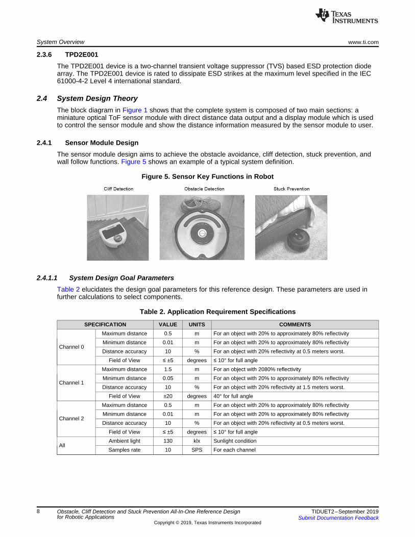
Figure 9. SFH203PFA Photodiode Spectral Response and Sunlight Power Within Photodiode SpectralBandwidth
2.4.1.11 Power Supply RecommendationsThe OPT3101 device requires 1.8- and 3.3-V supplies. There are two 1.8-V supplies (AVDD and DVDD)and two 3.3-V supplies (AVDD3 and IOVDD). AVDD and AVDD3 are analog supplies, DVDD and IOVDDare digital and I/O supplies. VDD_LED is not a device pin, but the supply connecting to the anode of theLED (Illumination source). The transmitter and receiver of the OPT3101 device operate at the samemodulation frequency (10 MHz). Any coupling from the transmitter switching to the AFE results in acrosstalk signal which affects the performance of the distance measurement. Achieving the lowestpossible crosstalk is critical for an accurate distance measurement system. Care should be taken toisolate all analog and switching supplies. Use ferrite beads with the highest impedance at 10 MHz (> 500Ω) in the series path of the supplies and decoupling capacitors with low impedance at fMOD on the suppliesvery close to the device. Negative voltage on the photodiode help to reduce the crosstalk. Voltages of –3.3V or –5 V is recommended to connect to the anode of the photodiode.
2.4.1.12 Sensor Module SchematicFigure 10 shows the schematic of sensor module based on the OPT3101 device.
Figure 10. Sensor Module Schematic

System Overview www.ti.com
16 TIDUET2–September 2019Submit Documentation Feedback
Copyright © 2019, Texas Instruments Incorporated
Obstacle, Cliff Detection and Stuck Prevention All-In-One Reference Designfor Robotic Applications
2.4.1.13 Isolation
2.4.1.13.1 CrosstalkCrosstalk is defined as the signal detected by the AFE system when there is no target before the system.It could also be the signals detected by the AFE when the target is too far away for the system to detect.Crosstalk plays a critical role in determining the absolute error and dynamic range of the system. Twotypes of crosstalk should be considered: electrical crosstalk and optical crosstalk.
Electrical crosstalk occurs due to electromagnetic coupling from the transmitter or digital switching nets onthe PCB to the analog side. Optical crosstalk occurs due to poor optical isolation or cover glass design.
The OPT3101 device has various built-in crosstalk correction capabilities outlined in the data sheet andcalibration guides of the device. However, it is important to minimize the crosstalk as much as possible toextract the best performance from the system.
2.4.1.13.2 Aggressor and Victim NetsThe OPT3101 AFE input nets INP and INM are high impedance nets suitable to electromagnetic coupling.There are 2 mechanisms of coupling that induces crosstalk, the voltage coupling and the current coupling.The OPT3101 AFE is immune to coupling from other frequencies apart from the modulation frequency.Hence, a ripple frequency from a DC/DC convertor or other clock frequencies on the board would not havesignificant impact to crosstalk; however, even a small amount of coupling from the TX0, TX1, and TX2nets would increase the crosstalk several fold.
Victims are always INP, INM, AVSS, AVDD, and AVDD3 nets. Aggressors are TX0, TX1, TX2, VSSL,Anode of emitters, IOVSS, DVDD.
2.4.1.13.3 Electrical IsolationA well-designed PCB layout, which is discussed in Section 4.3, is crucial to minimize the electricalcrosstalk and achieve the best performance. Even if utmost care is taken to improve the PCB layout, thelead length and the spacing of the through hole LEDs and photodiode which is chosen in this design,make the loop area large and make the electrical crosstalk quite high, reducing system dynamic range. Insuch cases an electrical isolation structure which is connected to AVSS is recommended around thephotodiode to isolate the photodiode from coupling. It is recommended that the material has goodelectrical conductivity, is magnetically inactive, and soldered AVSS exposed pads on the PCB.
2.4.1.13.4 Optical IsolationOptical isolation between the emitter and receiver is crucial to achieve good system performance. Havingany amount of light leakage from the emitter directly to the receiver could make the system unusable. Inthis reference design, a specific ring is designed to act electrical isolation and optical isolation.
See the Mechanical Specifications section in the Introduction to Time-of-Flight Long Range Proximity andDistance Sensor System Design User's Guide for more information.
2.4.1.13.5 Display Module DesignA display module with the MSP430FR2476 microcontroller is designed to control the OPT3101 device andget depth data from it. Then the distance information for proximity sensing is shown in the dual digitaldisplay. This reference design uses the 16-channel LED driver TLC59283 to drive the display so that IOsof the MCU can be saved.
A
B
C
D
E
F
G
DP
A
B
C
D
E
F
G
DP
DIG1 DIG2
IOVDD
DIG1 DIG2
SCLK
SIN
LAT
BLANK
VSS_IN
VSS_INUSB_5V
VSS_IN
VDD_3V3
IOVSS
VDD_3V3 IOVDD
VSS_IN
IOVDDIOVSS
SBWTCLK
SBWTDIO
IOVDD
IOVSS
TXD
IOVDD
IOVSS
RXD
D
B
E
F
G
C
DP
A
COM1
COM2
COM3
L1
L2
A
B
C
D
E
F
G
DP
A
B
C
D
E
F
G
DP
DIG3
D
B
E
F
G
C
DP
A
VDD_3V3
VSS_IN
SDA_S
SCL_S
VSYNC_RST
4. One TLC59283 for LED matrix
1. Delete extra LEDs
2. Add buzzer
3. Add On/Off control to minic Mechanical Switch
A
B
C
D
E
F
G
DP
A
B
C
D
E
F
G
DP
D
B
E
F
G
C
DP
A
IOVDD
COM4
COM5
COM6
DIG4 DIG5 DIG6
BUZ
IOVDD
SW
IOVDD
COL_SW
12
P1
Header 2
GP1
GP2
IOVSS
IOVDD DVCC32
P2.7/UCB1STE/CAP3.025
P2.6/UCA1TXD/UCA1SIMO/CAP1.319
RST/NMI/SBWTDIO1
P2.2/SYNC/ACLK/COMP0.111
P3.0/TA2.2/CAP0.012
P3.1/UCA1STE/CAP1.016
P3.2/UCB1SIMO/UCB1SDA/CAP3.227
P3.3/TA2.1/CAP0.113
P2.0/XOUT29
P2.1/XIN30
P4.0/TA3.1/CAP2.122
P4.1/TA3.0/CAP2.223
P4.2/TA3CLK/CAP2.324
P3.4/TA2CLK/COMP0OUT/CAP0.315
P3.5/UCB1CLK/TB0TRG/CAP3.126
P3.6/UCB1SOMI/UCB1SCL/CAP3.328
P3.7/TA3.2/CAP2.021
P2.3/TA2.0/CAP0.214
P2.4/UCA1CLK/CAP1.117
P1.0/UCB0STE/TA0CLK/A0/VEREF+7
P1.1/UCB0CLK/TA0.1/COMP0.0/A18
P1.2/UCB0SIMO/UCB0SDA/TA0.2/A2/VEREF-9
P1.3/UCB0SOMI/UCB0SCL/MCLK/A310
P1.4/UCA0TXD/UCA0SIMO/TA1.2/TCK/A4/VREF+3
P1.5/UCA0RXD/UCA0SOMI/TA1.1/TMS/A54
P1.6/UCA0CLK/TA1CLK/TDI/TCLK/A65
P1.7/UCA0STE/SMCLK/TDO/A76
TEST/SBWTCK2
DVSS31
VREG20
P2.5/UCA1RXD/UCA1SOMI/CAP1.218
PAD33
MSP430FR2476TRHB
U1
VSYNC_RST
SCL_S
SDA_S
TXD
RXD
GP1
SCLK
SIN
LAT
BLANK
GP2
BUZ
SBWTCLK
SW
IOVSS
IOVDD
SBWTDIO
CH1CH0 CH2
4. Change one MCU
1uF
C1
1uF
C2
10V0.1µF
C3
10V0.1µF
C4
10V0.1µF
C6
10V
0.1µF
C10
25V
1000pF
C12
COM1 COM2
DIG3
COM3
DIG4
COM4
DIG5
COM5
DIG6
COM6
47.0k
R1
470
R2
10k
R4
IOVSS
E1
D2
DIG213
C3
DP4
B15
A16
DIG114
F18
G17
E5
D6
C8
DP9
B10
A11
F12
G7
D1
LTD-6910HR
E1
D2
DIG213
C3
DP4
B15
A16
DIG114
F18
G17
E5
D6
C8
DP9
B10
A11
F12
G7
D2
LTD-6910HR
E1
D2
DIG213
C3
DP4
B15
A16
DIG114
F18
G17
E5
D6
C8
DP9
B10
A11
F12
G7
D3
LTD-6910HR
VCC1
NC2
IO13
GND4
IO25
TPD2E001DRLR
U3IN1
2
EN3
NC4
OUT5
GND
TLV70233DBVR
U2
VSS_IN
USB_5V
10V0.1µF
C8
VSS_IN VSS_IN
VBUS1
D-2
D+3
ID4
GND5
67
8
11
10
913
12
J4
ZX62R-B-5P(30)
1uF
C13
4
1
2
3
J1
4
1
2
3
J3
5
4
1
2
3
6
7
J2
47.0k
R3
GND1
SIN2
SCLK3
LAT4
OUT05
OUT16
OUT27
OUT38
OUT49
OUT510
OUT611
OUT712
OUT813
OUT914
OUT1015
OUT1116
OUT1217
OUT1318
OUT1419
OUT1520
BLANK21
SOUT22
IREF23
VCC24
TLC59282DBQ
U4
10V
10uF
C9
10V
10uF
C11
10V
10uF
C7
IOVSS
10k
R5
IOVSS
50V
100pF
C5
1
2
LS1
CMI-9653S-SMT-TR
3
1
2
Q4
RN2314
3
1
2
Q5
RN2314
3
1
2
Q6
RN2314
3
1
2
Q7
RN2314
3
1
2
Q8
RN2314
3
1
2
Q3
RN2314
3
1
2
Q2
RN2314
3
1
2
Q1
RN2314
www.ti.com System Overview
17TIDUET2–September 2019Submit Documentation Feedback
Copyright © 2019, Texas Instruments Incorporated
Obstacle, Cliff Detection and Stuck Prevention All-In-One Reference Designfor Robotic Applications
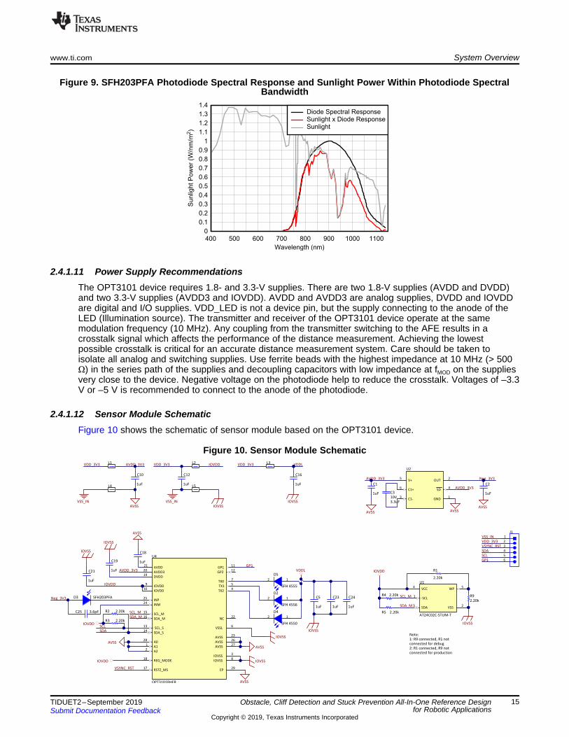
Figure 11. Display Board Schematic

Hardware, Software, Testing Requirements, and Test Results www.ti.com
18 TIDUET2–September 2019Submit Documentation Feedback
Copyright © 2019, Texas Instruments Incorporated
Obstacle, Cliff Detection and Stuck Prevention All-In-One Reference Designfor Robotic Applications
3 Hardware, Software, Testing Requirements, and Test Results
3.1 Required Hardware and Software
3.1.1 Hardware
3.1.1.1 Hardware OverviewThe whole design consists of two parts: a sensor board and display board. These two boards can beconnected by J2 (display board) and J1 (sensor board). Figure 12 shows the overview of the PCB for thesensor board and Figure 13 shows the display board. The user can also connect the sensor board to theirown controller system. A micro USB connector (J1) in the display module is used only for the 5-V powersupply input without data communication.
Figure 12. Sensor Board - Top View and Bottom View
Figure 13. Display Board - Top View and Bottom View
3.1.1.2 Programming Interface for the MSP430™ MCUThe J1 (display board) is reserved as the programming interface for the MCU. The designer can programthe MSP430 MCU using the JTAG port, Spy-Bi-Wire (SBW), and the bootloader BSL. In this referencedesign, SBW has been adopted for programming and is a two-wire Spy-Bi-Wire interface. Spy-Bi-Wire canbe used to interface with the MSP430 development tools and device programmers. Table 7 lists the Spy-Bi-Wire interface pin requirements. For further details on interfacing to development tools and deviceprogrammers, see the MSP430 Hardware Tools User's Guide.
Table 7. Spy-Bi-Wire Pin Requirements and Functions
J2 PINNUMBER DEVICE SIGNAL DIRECTION SBW FUNCTION
1 VSS — Ground supply

www.ti.com Hardware, Software, Testing Requirements, and Test Results
19TIDUET2–September 2019Submit Documentation Feedback
Copyright © 2019, Texas Instruments Incorporated
Obstacle, Cliff Detection and Stuck Prevention All-In-One Reference Designfor Robotic Applications
Table 7. Spy-Bi-Wire Pin Requirements and Functions (continued)J2 PIN
NUMBER DEVICE SIGNAL DIRECTION SBW FUNCTION
2 TEST/SBWTCK IN Spy-Bi-Wire clock input3 RST/NMI/SBWTDIO IN, OUT Spy-Bi-Wire data input and output4 VCC — Power supply
3.1.2 Firmware
3.1.2.1 Application Firmware DescriptionThe firmware of this reference design runs on the MSP430FR2476 device, in which an optical ToF-basedproximity sensing and system calibration is implemented. The firmware includes two parts: systemcalibration and sensor output capture . The system calibration firmware implements the OPT3101calibration procedure to get calibration parameters and save to an external EEPROM. The OPT3101device loads calibration parameters from the external EEPROM automatically after power on to configurethe registers inside the device over I²C and reads the measured distance data. Next, the firmwareconfigures the TLC59283 device to drive LED segments to display the distance. This system calibrationroutine must be done one time per board to get accurate distance measurements.
Table 8 lists the system components for the firmware of this reference design.
Table 8. TIDA-010021 Firmware System Components
ITEMS DESCRIPTIONIntegrated development environment (IDE) Code Composer Studio™ v9.0
Target MCU MSP430FR2476OPT3101 SDK OPT3101 software development kit (SDK)
LaunchPad™ Development Kit MSP430™ LaunchPad™MCU to OPT3101 connector P1.2 - SDA; P1.3 - SCL; P1.7 – GP1MCU to TLC59283 connector P2.3 – SIN; P2.4 – SCLK; P2.5 – LAT; P2.6 – BLANK
MCU to LaunchPad connector TEST – DEBUG; RESET- DEBUG; TXD – Reserved for user interface; RXD –Reserved for user interface
3.1.2.2 Prerequisites for Developing and RunningThis reference design board works as a stand-alone board after flashing the MCU firmware anddownloading it to the MSP430™ MCU. To develop and debug the firmware using TI’s Code ComposerStudio Integrated Development Environment (IDE), a MSP430FR2476 LaunchPad™ Development Kit orMSP-FET430UIF is required for programming and debugging the reference board. Figure 14 shows thehardware interconnections required between the design board and the LaunchPad for flashing the code inthis reference design. Make sure that the jumper has been removed before connecting the LaunchPadand TIDA-010021 board.

Hardware, Software, Testing Requirements, and Test Results www.ti.com
20 TIDUET2–September 2019Submit Documentation Feedback
Copyright © 2019, Texas Instruments Incorporated
Obstacle, Cliff Detection and Stuck Prevention All-In-One Reference Designfor Robotic Applications
Figure 14. LaunchPad™ and TIDA-010077 Board Connections Diagram
Make sure to download and install the following prerequisites to the computer:• Code Composer Studio™ v9.0• TIDA-010077_RevA Firmware
3.1.2.3 Programming the MSP430™The user can edit and program the firmware of the MSP430™ MCU. The TIDA-010077 boardprogramming instructions follow:1. Import the TIDA_010077_RevA project using TI’s Code Composer Studio software.2. Connect the LaunchPad programmer to the TIDA-010077 board, as Figure 14 shows.3. Build the project by clicking the Build button (hammer icon), which if run successfully, appears as
Figure 15 shows.4. Click the Debug button (bug icon) as Figure 15 shows.

www.ti.com Hardware, Software, Testing Requirements, and Test Results
21TIDUET2–September 2019Submit Documentation Feedback
Copyright © 2019, Texas Instruments Incorporated
Obstacle, Cliff Detection and Stuck Prevention All-In-One Reference Designfor Robotic Applications
Figure 15. Build and Debug Using Code Composer Studio™ From TI
3.1.2.4 OPT3101 SDKThe OPT3101 software development kit (SDK) provides a C++ library of functions to control and calibratesystems using the OPT3101 device, which is a ToF-based, long-range proximity and distance sensoranalog front end (AFE).
The OPT3101 SDK features follow:1. Enables access to registers by name instead of physical address2. Enables control and access to groups of registers to achieve specific functionality3. Contains data types (classes) to hold, analyze, and report calibration data4. Allows templatizing of classes for environment and host controls
For more SDK details, see the OPT3101 software development kit (SDK).
3.1.2.5 User Application Flow Charts
3.1.2.5.1 Distance Capture Flow ChartFigure 16 shows the flow chart of distance data capture from the OPT3101 firmware in the MCU. TI offersthis firmware example in which system hardware initialization, OPT3101 calibration parameters loading,and repeatedly distance data capture has been implemented. Calibration parameters are in externalEEPROM and load automatically to the OPT3101 device, the user must run the system calibration routinefirst for new projects. Additionally, this firmware reserves the UART communication interface for directlyreading and writing OPT3101 registers. The user can use this interface to debug or develop a GUI on thePC.

Start
System peripherals
initialize
Communication, LED
Display initialize
OPT3101 reset
OPT3101 initialize
OPT3101 Load Calibration
Parameters from EEPROM
Trigger Measurement
Read Measurement Results
Display distance on LED
segments
Hardware, Software, Testing Requirements, and Test Results www.ti.com
22 TIDUET2–September 2019Submit Documentation Feedback
Copyright © 2019, Texas Instruments Incorporated
Obstacle, Cliff Detection and Stuck Prevention All-In-One Reference Designfor Robotic Applications
Figure 16. Proximity Application Flow Chart
3.1.2.5.2 System Calibration Flow ChartSystem calibration is critical for this design. See the OPT3101 Distance Sensor System Calibration User'sGuide and the How to Set Up and Calibrate OPT3101 Based Systems for Proximity Sensing User's Guidefor more details.
Figure 17 shows the system calibration flow chart. This calibration routine must be done one time perTIDA-010077 board and save the calibration parameters to external EEPROM memory. Once the datacapture application runs, the OPT3101 device loads the calibration parameters from the externalEEPROM automatically after power on.

Start
System peripherals
initialize
OPT3101 reset
OPT3101 initialize
Frequency Calibration
(Optional)
Cover photodiode and
Illumination crosstalk
calibration
Remove cover, set target
object at reference
distance
Phase Offset Calibration
Save calibration data
to FRAM
End
www.ti.com Hardware, Software, Testing Requirements, and Test Results
23TIDUET2–September 2019Submit Documentation Feedback
Copyright © 2019, Texas Instruments Incorporated
Obstacle, Cliff Detection and Stuck Prevention All-In-One Reference Designfor Robotic Applications
Figure 17. System Calibration Flow Chart
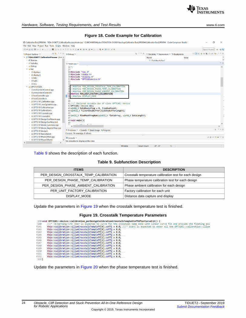
Choose the specific calibration step and comment out the others as Figure 18 shows. The referencedistance setting should ensure the received signal amplitude is high (AMP_OUT > 10000).
Hardware, Software, Testing Requirements, and Test Results www.ti.com
24 TIDUET2–September 2019Submit Documentation Feedback
Copyright © 2019, Texas Instruments Incorporated
Obstacle, Cliff Detection and Stuck Prevention All-In-One Reference Designfor Robotic Applications
Figure 18. Code Example for Calibration
Table 9 shows the description of each function.
Table 9. Subfunction Description
ITEMS DESCRIPTIONPER_DESIGN_CROSSTALK_TEMP_CALIBRATION Crosstalk temperature calibration test for each design
PER_DESIGN_PHASE_TEMP_CALIBRATION Phase temperature calibration test for each designPER_DESIGN_PHASE_AMBIENT_CALIBRATION Phase ambient calibration for each design
PER_UNIT_FACTORY_CALIBRATION Factory calibration for each unitDISPLAY_MODE Distance data capture and display
Update the parameters in Figure 19 when the crosstalk temperature test is finished.
Figure 19. Crosstalk Temperature Parameters
Update the parameters in Figure 20 when the phase temperature test is finished.

www.ti.com Hardware, Software, Testing Requirements, and Test Results
25TIDUET2–September 2019Submit Documentation Feedback
Copyright © 2019, Texas Instruments Incorporated
Obstacle, Cliff Detection and Stuck Prevention All-In-One Reference Designfor Robotic Applications
Figure 20. Phase Temperature Parameters
Update the parameters in Figure 21 when the phase ambient test is finished.
Figure 21. Phase Ambient Parameters
3.2 Testing and ResultsThe test results for this optical object distance sensing are divided into multiple sections that cover how toset up the test, the system performance under different ambient conditions and different target objectcolors.
3.2.1 Test SetupThis section describes in detail the materials which are used for testing in the lab and how to set up thetest platform step-by-step. Objects in different colors and other interference testing was also performed toverify how the reference design acts in different environments.
3.2.1.1 Test Setup PreparationTesting the performance of the reference design and proximity sensor board requires some materials andequipment for preparation. Table 10 lists the materials required for the test setup and their basic usage.
Table 10. Materials for Test Setup
MATERIALS USAGE COMMENTS
Computer Program, debug and continuously capture measurement data Code Composer Studio™ v9.0downloaded and installed
TIDA-010021 display board Control the sensor board and read out the dataTIDA-010021 sensor board Measure the distance of target objectBand tape Measure the actual distance of target object Minimum 2 meters
Photo meter Measure the ambient light Maximum range supports up to130 klx
Power meter Test the power consumption of sensor module

Hardware, Software, Testing Requirements, and Test Results www.ti.com
26 TIDUET2–September 2019Submit Documentation Feedback
Copyright © 2019, Texas Instruments Incorporated
Obstacle, Cliff Detection and Stuck Prevention All-In-One Reference Designfor Robotic Applications
3.2.1.2 Test Setup ProcedureThe following steps show how to set up the test platform in the lab during the detailed testing anddebugging:• Make sure that the firmware has been programmed into the MCU.• Connect the sensor board and display board.• Connect the computer and sensor board through USB. The USB is only used for the power input of the
display board without data communication.• Mount the sensor into a specified fixture.
3.2.2 Test ResultsIn this test, a wall with different color acts as a sensing target to simulate a real application. Threeapplication scenes, including darkness operation and sunlight operation, are tested. The target for 3channels (TX0, TX1, TX2) are tested separately.
3.2.2.1 Scene 1 - Operation in Daytime With Light on (210 lux Ambient Light)Scene 1 aims to test the sensor performance in daytime with the room light on (210 lux ambient lightenvironment).
3.2.2.1.1 White Wall as TargetA white wall acts as the target. Figure 22 shows the test setup.
Figure 22. White Wall as Test Target

Actual Distance (mm)
Mea
sure
me
nt
Dis
tan
ce (
mm
)
0 20 40 60 80 100 120 140 1600
25
50
75
100
125
150
175
D017
Actual Distance (mm)
Err
or
(%)
0 20 40 60 80 100 120 140 160-2
-1
0
1
2
3
4
5
6
7
D007
Actual Distance (mm)
Measure
ment D
ista
nce (
mm
)
5 10 15 20 25 30 35 40 45 505
10
15
20
25
30
35
40
45
50
D014
Actual Distance (mm)
Err
or
(%)
5 10 15 20 25 30 35 40 45 50-6
-4
-2
0
2
4
6
8
D004
www.ti.com Hardware, Software, Testing Requirements, and Test Results
27TIDUET2–September 2019Submit Documentation Feedback
Copyright © 2019, Texas Instruments Incorporated
Obstacle, Cliff Detection and Stuck Prevention All-In-One Reference Designfor Robotic Applications
Figure 23 shows the distance measured by the sensor when a white wall acts as the target for TX0 andFigure 24 shows the error (in percent) with regards to distance.
Figure 23. Measurement Distance vs Actual Distance - TX0White Wall
Figure 24. Error % vs Distance - TX0 White Wall
Figure 25 shows the distance measured by the sensor when a white wall acts as the target for TX1 andFigure 26 shows the error (in percent) with regards to distance.
Figure 25. Measurement Distance vs Actual Distance - TX1White Wall
Figure 26. Error % vs Distance - TX1 White Wall
Figure 27 shows the distance measured by the sensor when a white wall acts as the target for TX2 andFigure 28 shows the error (in percent) with regards to distance.

Actual Distance (mm)
Mea
sure
me
nt
Dis
tan
ce (
mm
)
5 10 15 20 25 30 35 40 45 505
10
15
20
25
30
35
40
45
50
55
D020
Actual Distance (mm)
Err
or
(%)
5 10 15 20 25 30 35 40 45 500
0.5
1
1.5
2
2.5
3
3.5
4
4.5
5
5.5
6
6.5
7
7.5
D010
Hardware, Software, Testing Requirements, and Test Results www.ti.com
28 TIDUET2–September 2019Submit Documentation Feedback
Copyright © 2019, Texas Instruments Incorporated
Obstacle, Cliff Detection and Stuck Prevention All-In-One Reference Designfor Robotic Applications
Figure 27. Measurement Distance vs Actual Distance - TX2White Wall
Figure 28. Error % vs Distance - TX2 White Wall
3.2.2.1.2 Green Wall as TargetA green wall acts as the target. Figure 29 shows the test setup.
Figure 29. Green Wall as Test Target
Figure 30 shows the distance measured by the sensor when a green wall acts as the target for TX0 andFigure 31 shows the error (in percent) with regards to distance.

Actual Distance (mm)
Mea
sure
me
nt
Dis
tan
ce (
mm
)
0 20 40 60 80 100 120 140 1600
25
50
75
100
125
150
175
D016
Actual Distance (mm)
Err
or
(%)
0 20 40 60 80 100 120 140 160-2
0
2
4
6
8
D006
Actual Distance (mm)
Mea
sure
me
nt
Dis
tan
ce (
mm
)
5 10 15 20 25 30 35 40 45 505
10
15
20
25
30
35
40
45
50
D012
Actual Distance (mm)
Err
or
(%)
5 10 15 20 25 30 35 40 45 50-6
-4
-2
0
2
4
6
8
D003
www.ti.com Hardware, Software, Testing Requirements, and Test Results
29TIDUET2–September 2019Submit Documentation Feedback
Copyright © 2019, Texas Instruments Incorporated
Obstacle, Cliff Detection and Stuck Prevention All-In-One Reference Designfor Robotic Applications
Figure 30. Measurement Distance vs Actual Distance - TX0Green Wall
Figure 31. Error % vs Distance - TX0 Green Wall
Figure 32 shows the distance measured by the sensor when a green wall acts as the target for TX1 andFigure 33 shows the error (in percent) with regards to distance.
Figure 32. Measurement Distance vs Actual Distance - TX1Green Wall
Figure 33. Error % vs Distance - TX1 Green Wall
Figure 34 shows the distance measured by the sensor when a green wall acts as the target for TX2 andFigure 35 shows the error (in percent) with regards to distance.

Actual Distance (mm)
Mea
sure
me
nt
DIs
tan
ce (
mm
)
5 10 15 20 25 30 35 40 45 505
10
15
20
25
30
35
40
45
50
55
D019
Actual Distance (mm)
Err
or
(%)
5 10 15 20 25 30 35 40 45 500
1
2
3
4
5
6
D009
Hardware, Software, Testing Requirements, and Test Results www.ti.com
30 TIDUET2–September 2019Submit Documentation Feedback
Copyright © 2019, Texas Instruments Incorporated
Obstacle, Cliff Detection and Stuck Prevention All-In-One Reference Designfor Robotic Applications
Figure 34. Measurement Distance vs Actual Distance - TX2Green Wall
Figure 35. Error % vs Distance - TX2 Green Wall
3.2.2.1.3 Black Wall as TargetA black wall acts as the target. Figure 36 shows the test setup.
Figure 36. Black Wall as Test Target
Figure 37 shows the distance measured by the sensor when a black wall acts as the target for TX0 andFigure 38 shows the error (in percent) with regards to distance.

Actual Distance (mm)
Mea
sure
me
nt
Dis
tan
ce (
mm
)
0 20 40 60 80 100 120 140 1600
25
50
75
100
125
150
175
D015
Actual Distance (mm)
Err
or
(%)
0 20 40 60 80 100 120 140 160-8
-6
-4
-2
0
2
4
D005
Actual Distance (mm)
Mea
sure
me
nt
Dis
tan
ce (
mm
)
5 10 15 20 25 30 35 40 45 505
10
15
20
25
30
35
40
45
50
D011
Actual Distance (mm)
Err
or
(%)
5 10 15 20 25 30 35 40 45 50-7.5
-7
-6.5
-6
-5.5
-5
-4.5
-4
-3.5
-3
D002
www.ti.com Hardware, Software, Testing Requirements, and Test Results
31TIDUET2–September 2019Submit Documentation Feedback
Copyright © 2019, Texas Instruments Incorporated
Obstacle, Cliff Detection and Stuck Prevention All-In-One Reference Designfor Robotic Applications
Figure 37. Measurement Distance vs Actual Distance - TX0Black Wall
Figure 38. Error % vs Distance - TX0 Black Wall
Figure 39 shows the distance measured by the sensor when a black wall acts as the target for TX1 andFigure 40 shows the error (in percent) with regards to distance.
Figure 39. Measurement Distance vs Actual Distance - TX1Black Wall
Figure 40. Error % vs Distance - TX1 Black Wall
Figure 41 shows the distance measured by the sensor when a black wall acts as the target for TX2 andFigure 42 shows the error (in percent) with regards to distance.

Actual Distance (mm)
Mea
sure
me
nt
Dis
tan
ce (
mm
)
5 10 15 20 25 30 35 40 45 505
10
15
20
25
30
35
40
45
50
D018
Actual Distance (mm)
Err
or
(%)
5 10 15 20 25 30 35 40 45 50-7
-6
-5
-4
-3
-2
-1
0
D008
Hardware, Software, Testing Requirements, and Test Results www.ti.com
32 TIDUET2–September 2019Submit Documentation Feedback
Copyright © 2019, Texas Instruments Incorporated
Obstacle, Cliff Detection and Stuck Prevention All-In-One Reference Designfor Robotic Applications
Figure 41. Measurement Distance vs Actual Distance - TX2Black Wall
Figure 42. Error % vs Distance - TX2 Black Wall
The test results in the previous images show that the target with a different color may affect the NIRreflection but the sensor is not sensitive to object color. The measured distance error is within the scope ofpre-defined parameters for different color walls.
3.2.2.2 Scene 2 - Darkness OperationScene 2 aims to test the sensor performance under darkness operation, for example, evening or nightwhen there is no ambient light or low ambient light. Figure 43 shows the test setup under a darkenvironment.
Figure 43. Darkness Operation
For the darkness operation, only TX1 is chosen and a white wall acts as the target for the test. Comparingwith the same position of Scene 1, sensor performance under darkness operation can be observed andthe effects of low ambient light can be concluded. In Figure 44, the red line shows the test resultscomparing with the black line which is sensor performance in Scene 1.
Figure 44 shows that sensor performance under darkness operation is good or even better comparingScene 1.

Actual Distance (mm)
Me
asu
rem
en
t E
rro
r (%
)
0 20 40 60 80 100 120 140 160-4
-2
0
2
4
6
8
D021
www.ti.com Hardware, Software, Testing Requirements, and Test Results
33TIDUET2–September 2019Submit Documentation Feedback
Copyright © 2019, Texas Instruments Incorporated
Obstacle, Cliff Detection and Stuck Prevention All-In-One Reference Designfor Robotic Applications
Figure 44. Operation in Darkness Comparing With Scene 1
3.2.2.3 Scene 3 - Operation Under Sunlight (86 klx Ambient Light)Scene 3 aims to test the sensor performance under a sunlight environment, for example, when thesunshine comes into the room at noon. Figure 45 shows the test setup at 86-klx sunlight environment.

Hardware, Software, Testing Requirements, and Test Results www.ti.com
34 TIDUET2–September 2019Submit Documentation Feedback
Copyright © 2019, Texas Instruments Incorporated
Obstacle, Cliff Detection and Stuck Prevention All-In-One Reference Designfor Robotic Applications
Figure 45. 86-klx Ambient Light Operation
For the high ambient light operation, only TX1 is chosen and a white wall acts as the target for the test.Comparing with the same position of Scene 1, the sensor performance under sunlight operation can beobserved and the effects of high ambient light can be concluded. In Figure 46, the red line shows the testresults comparing with the black line which is the sensor performance in Scene 1.

Actual Distance (mm)
Me
asu
rem
en
t E
rro
r (%
)
0 20 40 60 80 100 120 140 160-2
-1
0
1
2
3
4
5
6
7
D022
www.ti.com Hardware, Software, Testing Requirements, and Test Results
35TIDUET2–September 2019Submit Documentation Feedback
Copyright © 2019, Texas Instruments Incorporated
Obstacle, Cliff Detection and Stuck Prevention All-In-One Reference Designfor Robotic Applications
Figure 46. Operation Under Sunlight Comparing With Scene 1
Figure 46 shows that sensor support high ambient light operation and performance is much better thanother optical technics for proximity sensing.
3.2.2.4 Power ConsumptionThe sensor can run in normal operating mode (10 SPS) and low power mode. In low power mode, thesensor wakes up every 1 s and outputs 1 sample. When a movement is detected, the sensor runs innormal operating mode.
Table 11. Consumption at Ambient Temperature
PARAMETER MIN MAX UNIT COMMENTSHW standby 80 µA Deep sleep mode
Operating current 25 90 mA Continuous measuring distance at 128 sub framesper sample and 31.25 samples per second
Operating power consumption 82.5 297 mW 3.3-V power supplyCurrent in low power mode 3 9 mA Wake up every 1 sPower consumption at low
power mode 10 30 mW Wake up every 1 s for one sample (128 sub frames)

Design Files www.ti.com
36 TIDUET2–September 2019Submit Documentation Feedback
Copyright © 2019, Texas Instruments Incorporated
Obstacle, Cliff Detection and Stuck Prevention All-In-One Reference Designfor Robotic Applications
4 Design Files
4.1 SchematicsTo download the schematics, see the design files at TIDA-010077.
4.2 Bill of MaterialsTo download the bill of materials (BOM), see the design files at TIDA-010077.
4.3 PCB Layout RecommendationsReducing the coupling between the transmitter and receiver is critical to achieve good systemperformance. Minimize the area of transmitter current carrying loop through the LED supply decouplingcapacitor, LED and the AFE pins TX*, VSSL. Also minimize the receiver loop involving the photodiode,matching capacitor and the AFE pins INP, INM. It is recommended to use the layout as it is to get the bestperformance. If changes are needed, the following guidelines must be strictly followed to keep thecrosstalk between transmitter and receiver low.• A 4-layer board is proposed, so that all the analog and digital supplies can be well isolated from each
other.• Place the photodiode and LED oriented orthogonal to each other.• Minimize the area of the transmitter current carrying loop involving LED, VDD_LED to VSSL
decoupling capacitor, and AFE.• Minimize the area of the receiver loop involving photodiode, matching capacitor and AFE.• Shield the receiver loop using AVSS ground in the top and bottom PCB layers. Also place a shielding
ring around the photodiode and connect the shielding ring to AVSS. This shielding ring reduces theelectrical and optical crosstalk.
• Shield the transmitter loop using IOVSS ground in all the PCB layers. Also place a shielding ringaround the LED and connect the shielding ring to IOVSS.
• The LED terminals and the photodiode terminals must not be directly exposed to each other. Any smallamount of capacitive coupling between photodiode and LED terminals result in huge crosstalk.Grounded metal rings around the photodiode and LED improves shielding.
• Use vias around the transmitter and receiver loops in the respective ground planes to improve theshielding.
• Connect the device thermal pad to AVSS.• Do not overlap different ground planes, keep them well isolated.
See the Introduction to Time-of-Flight Long Range Proximity and Distance Sensor System Design User'sGuide for more information.
4.3.1 Layout PrintsTo download the layer plots, see the design files at TIDA-010077.
4.4 Altium ProjectTo download the Altium Designer® project files, see the design files at TIDA-010077.
4.5 Gerber FilesTo download the Gerber files, see the design files at TIDA-010077.
4.6 Assembly DrawingsTo download the assembly drawings, see the design files at TIDA-010077.

www.ti.com Software Files
37TIDUET2–September 2019Submit Documentation Feedback
Copyright © 2019, Texas Instruments Incorporated
Obstacle, Cliff Detection and Stuck Prevention All-In-One Reference Designfor Robotic Applications
5 Software FilesTo download the software files, see the design files at TIDA-010077.
6 Related Documentation1. Texas Instruments, OPT3101 ToF-Based Long-Range Proximity and Distance Sensor AFE Data Sheet2. Texas Instruments, Introduction to Time-of-Flight Long Range Proximity and Distance Sensor System
Design User's Guide3. Texas Instruments, OPT3101 Distance Sensor System Calibration User's Guide4. Texas Instruments, OPT3101 System Estimator User's Guide
6.1 TrademarksE2E, LaunchPad, MSP430, Code Composer Studio are trademarks of Texas Instruments.Altium Designer is a registered trademark of Altium LLC or its affiliated companies.All other trademarks are the property of their respective owners.
6.2 Third-Party Products DisclaimerTI'S PUBLICATION OF INFORMATION REGARDING THIRD-PARTY PRODUCTS OR SERVICES DOESNOT CONSTITUTE AN ENDORSEMENT REGARDING THE SUITABILITY OF SUCH PRODUCTS ORSERVICES OR A WARRANTY, REPRESENTATION OR ENDORSEMENT OF SUCH PRODUCTS ORSERVICES, EITHER ALONE OR IN COMBINATION WITH ANY TI PRODUCT OR SERVICE.
7 TerminologyFoV — Field of View
AFE — Analog Front End
NIR — Near Infrared
ToF — Time of Flight
HDR — High-Dynamic Range
MCU — Microcontroller unit
ESD — Electrostatic discharge
8 About the AuthorYICHANG (RICHARD) WANG is a Systems Architect at Texas Instruments, where he is responsible fordeveloping reference design solutions for the industrial segment. Richard brings to this role his extensiveexperience in home appliances including power electronics, high-frequency DC/DC, AC/DC converters,analog circuit design, sensors and so on. Richard got his master’s degree in Electrical Engineering andAutomation from Nanjing University of Aeronautics and Astronautics, China.
FANCHEN (PATRICK) ZENG is a field analog application engineer at Texas Instruments, where he isresponsible for supporting customers from the appliances sector. Patrick brings to this role his extensiveexperience in home appliances, including analog circuit design, in-depth system knowledge, identifyingand solving application design challenges, and so forth.

IMPORTANT NOTICE AND DISCLAIMER
TI PROVIDES TECHNICAL AND RELIABILITY DATA (INCLUDING DATASHEETS), DESIGN RESOURCES (INCLUDING REFERENCEDESIGNS), APPLICATION OR OTHER DESIGN ADVICE, WEB TOOLS, SAFETY INFORMATION, AND OTHER RESOURCES “AS IS”AND WITH ALL FAULTS, AND DISCLAIMS ALL WARRANTIES, EXPRESS AND IMPLIED, INCLUDING WITHOUT LIMITATION ANYIMPLIED WARRANTIES OF MERCHANTABILITY, FITNESS FOR A PARTICULAR PURPOSE OR NON-INFRINGEMENT OF THIRDPARTY INTELLECTUAL PROPERTY RIGHTS.These resources are intended for skilled developers designing with TI products. You are solely responsible for (1) selecting the appropriateTI products for your application, (2) designing, validating and testing your application, and (3) ensuring your application meets applicablestandards, and any other safety, security, or other requirements. These resources are subject to change without notice. TI grants youpermission to use these resources only for development of an application that uses the TI products described in the resource. Otherreproduction and display of these resources is prohibited. No license is granted to any other TI intellectual property right or to any thirdparty intellectual property right. TI disclaims responsibility for, and you will fully indemnify TI and its representatives against, any claims,damages, costs, losses, and liabilities arising out of your use of these resources.TI’s products are provided subject to TI’s Terms of Sale (www.ti.com/legal/termsofsale.html) or other applicable terms available either onti.com or provided in conjunction with such TI products. TI’s provision of these resources does not expand or otherwise alter TI’s applicablewarranties or warranty disclaimers for TI products.
Mailing Address: Texas Instruments, Post Office Box 655303, Dallas, Texas 75265Copyright © 2019, Texas Instruments Incorporated