Embed Size (px)
Citation preview

TLC5628C, TLC5628IOCTAL 8-BIT DIGITAL-TO-ANALOG CONVERTERS
SLAS089E – NOVEMBER 1994 – REVISED APRIL 1997
1POST OFFICE BOX 655303 • DALLAS, TEXAS 75265
Eight 8-Bit Voltage Output DACs
5-V Single-Supply Operation
Serial Interface
High-Impedance Reference Inputs
Programmable 1 or 2 Times Output Range
Simultaneous Update Facility
Internal Power-On Reset
Low-Power Consumption
Half-Buffered Output
applications
Programmable Voltage Sources
Digitally Controlled Amplifiers/Attenuators
Mobile Communications
Automatic Test Equipment
Process Monitoring and Control
Signal Synthesis
description
The TLC5628C and TLC5628I are octal 8-bit voltage output digital-to-analog converters (DACs) with bufferedreference inputs (high impedance). The DACs produce an output voltage that ranges between either one or twotimes the reference voltages and GND and are monotonic. The device is simple to use, running from a singlesupply of 5 V. A power-on reset function is incorporated to ensure repeatable start-up conditions.
Digital control of the TLC5628C and TLC5628I are over a simple three-wire serial bus that is CMOS compatibleand easily interfaced to all popular microprocessor and microcontroller devices. The 12-bit command wordcomprises eight bits of data, three DAC select bits, and a range bit, the latter allowing selection between thetimes 1 or times 2 output range. The DAC registers are double buffered, allowing a complete set of new valuesto be written to the device, then all DAC outputs are updated simultaneously through control of LDAC. The digitalinputs feature Schmitt triggers for high-noise immunity.
The 16-terminal small-outline (D) package allows digital control of analog functions in space-criticalapplications. The TLC5628C is characterized for operation from 0°C to 70°C. The TLC5628I is characterizedfor operation from –40°C to 85°C. The TLC5628C and TLC5628I do not require external trimming.
AVAILABLE OPTIONS
PACKAGE
TASMALL OUTLINE
(DW)PLASTIC DIP
(N)
0°C to 70°C TLC5628CDW TLC5628CN
–40°C to 85°C TLC5628IDW TLC5628IN
Please be aware that an important notice concerning availability, standard warranty, and use in critical applications ofTexas Instruments semiconductor products and disclaimers thereto appears at the end of this data sheet.
PRODUCTION DATA information is current as of publication date.Products conform to specifications per the terms of Texas Instrumentsstandard warranty. Production processing does not necessarily includetesting of all parameters.
Copyright 1997, Texas Instruments Incorporated
1
2
3
4
5
6
7
8
16
15
14
13
12
11
10
9
DACBDACAGND
DATACLKVDD
DACEDACF
DACCDACDREF1LDACLOADREF2DACHDACG
N OR DW PACKAGE(TOP VIEW)
TLC5628C, TLC5628IOCTAL 8-BIT DIGITAL-TO-ANALOG CONVERTERS
SLAS089E – NOVEMBER 1994 – REVISED APRIL 1997
2 POST OFFICE BOX 655303 • DALLAS, TEXAS 75265
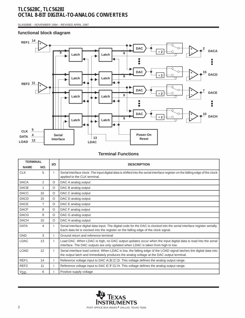
functional block diagram
SerialInterface
× 2DAC
DAC× 2
× 2DAC
DAC× 2
LDAC
REF1 +–
+–
+–
+–
+–
+–
REF2
CLK
DATA
LOAD
DACA
DACD
DACE
DACH
9 8
8
8
8
LatchLatch
Latch Latch
LatchLatch
Latch Latch
Power-OnReset
14
11
5
4
1213
2
15
7
10
Terminal Functions
TERMINALI/O DESCRIPTION
NAME NO.I/O DESCRIPTION
CLK 5 I Serial interface clock. The input digital data is shifted into the serial interface register on the falling edge of the clockapplied to the CLK terminal.
DACA 2 O DAC A analog output
DACB 1 O DAC B analog output
DACC 16 O DAC C analog output
DACD 15 O DAC D analog output
DACE 7 O DAC E analog output
DACF 8 O DAC F analog output
DACG 9 O DAC G analog output
DACH 10 O DAC H analog output
DATA 4 I Serial interface digital data input. The digital code for the DAC is clocked into the serial interface register serially.Each data bit is clocked into the register on the falling edge of the clock signal.
GND 3 I Ground return and reference terminal
LDAC 13 I Load DAC. When LDAC is high, no DAC output updates occur when the input digital data is read into the serialinterface. The DAC outputs are only updated when LDAC is taken from high to low.
LOAD 12 I Serial interface load control. When LDAC is low, the falling edge of the LOAD signal latches the digital data intothe output latch and immediately produces the analog voltage at the DAC output terminal.
REF1 14 I Reference voltage input to DAC A B C D. This voltage defines the analog output range.
REF2 11 I Reference voltage input to DAC E F G H. This voltage defines the analog output range.
VDD 6 I Positive supply voltage

TLC5628C, TLC5628IOCTAL 8-BIT DIGITAL-TO-ANALOG CONVERTERS
SLAS089E – NOVEMBER 1994 – REVISED APRIL 1997
3POST OFFICE BOX 655303 • DALLAS, TEXAS 75265
detailed description
The TLC5628 is implemented using eight resistor-string DACs. The core of each DAC is a single resistor with256 taps, corresponding to the 256 possible codes listed in Table 1. One end of each resistor string is connectedto GND and the other end is fed from the output of the reference input buffer. Monotonicity is maintained by useof the resistor strings. Linearity depends upon the matching of the resistor segments and upon the performanceof the output buffer. Since the inputs are buffered, the DACs always present a high-impedance load to thereference sources. There are two input reference terminals; REF1 is used for DACA through DACD and REF2is used by DACE through DACH.
Each DAC output is buffered by a configurable-gain output amplifier, that can be programmed to times 1 or times2 gain.
On power up, the DACs are reset to CODE 0.
Each output voltage is given by:
VO(DACA|B|C|D|E|F|G|H) REFCODE256
(1RNG bit value)
where CODE is in the range 0 to 255 and the range (RNG) bit is a 0 or 1 within the serial control word.
Table 1. Ideal Output Transfer
D7 D6 D5 D4 D3 D2 D1 D0 OUTPUT VOLTAGE
0 0 0 0 0 0 0 0 GND
0 0 0 0 0 0 0 1 (1/256) × REF (1+RNG)
• • • • • • • • •
• • • • • • • • •
0 1 1 1 1 1 1 1 (127/256) × REF (1+RNG)
1 0 0 0 0 0 0 0 (128/256) × REF (1+RNG)
• • • • • • • • •
• • • • • • • • •
1 1 1 1 1 1 1 1 (255/256) × REF (1+RNG)
data interface
With LOAD high, data is clocked into the DATA terminal on each falling edge of CLK. Once all data bits havebeen clocked in, LOAD is pulsed low to transfer the data from the serial input register to the selected DAC asshown in Figure 1. When LDAC is low, the selected DAC output voltage is updated when LOAD goes low. WhenLDAC is high during serial programming, the new value is stored within the device and can be transferred tothe DAC output at a later time by pulsing LDAC low as shown in Figure 2. Data is entered most significant bit(MSB) first. Data transfers using two 8-clock cycle periods are shown in Figures 3 and 4.
A2 A1 A0 RNG D7 D6 D5 D4 D2 D1 D0
DAC Update
CLK
DATA
LOAD
tsu(DATA-CLK)tv(DATA-CLK)
tsu(CLK-LOAD)tw(LOAD)
tsu(LOAD-CLK)
Figure 1. LOAD-Controlled Update (LDAC = Low)

TLC5628C, TLC5628IOCTAL 8-BIT DIGITAL-TO-ANALOG CONVERTERS
SLAS089E – NOVEMBER 1994 – REVISED APRIL 1997
4 POST OFFICE BOX 655303 • DALLAS, TEXAS 75265
data interface (continued)
CLK
DATA
LOAD
LDAC
DAC Update
A2 A1 A0 RNG D7 D6 D5 D4 D2 D1 D0
tsu(DATA-CLK)tv(DATA-CLK)
tw(LDAC)
tsu(LOAD–LDAC)
Figure 2. LDAC-Controlled Update
ÎÎÎÎÎÎÎÎÎÎ
ÎÎÎÎÎÎ
ÎÎÎÎÎÎ
A1 A0 RNG D7 D6 D5 D4 D3 D2 D1 D0
CLK
DATA
LOAD
LDAC
CLK Low
A2
Figure 3. Load-Controlled Update Using 8-Bit Serial Word (LDAC = Low)
ÎÎÎÎÎÎÎÎÎÎ
ÎÎÎÎÎÎÎÎ
ÎÎÎÎÎÎÎÎ
A1 A0 RNG D7 D6 D5 D4 D3 D2 D1 D0
CLK
DATA
LOAD
LDAC
CLK Low
A2
Figure 4. LDAC-Controlled Update Using 8-Bit Serial Word
Table 2 lists the A2, A1, and A0 bits and the selection of the updated DACs. The RNG bit controls the DAC outputrange. When RNG = low, the output range is between the applied reference voltage and GND, and whenRNG = high, the range is between twice the applied reference voltage and GND.
Table 2. Serial Input Decode
A2 A1 A0 DAC UPDATED
0 0 0 DACA
0 0 1 DACB
0 1 0 DACC
0 1 1 DACD
1 0 0 DACE
1 0 1 DACF
1 1 0 DACG
1 1 1 DACH

TLC5628C, TLC5628IOCTAL 8-BIT DIGITAL-TO-ANALOG CONVERTERS
SLAS089E – NOVEMBER 1994 – REVISED APRIL 1997
5POST OFFICE BOX 655303 • DALLAS, TEXAS 75265
linearity, offset, and gain error using single-end supplies
When an amplifier is operated from a single supply, the voltage offset can still be either positive or negative. Witha positive offset voltage, the output voltage changes on the first code change. With a negative offset the outputvoltage may not change with the first code depending on the magnitude of the offset voltage.
The output amplifier, therefore, attempts to drive the output to a negative voltage. However, because the mostnegative supply rail is ground, the output cannot drive below ground.
The output voltage remains at 0 V until the input code value produces a sufficient output voltage to overcomethe inherent negative offset voltage, resulting in the transfer function shown in Figure 5.
DAC Code
OutputVoltage
0 V
NegativeOffset
Figure 5. Effect of Negative Offset (Single Supply)
This offset error, not the linearity error, produces the breakpoint. The transfer function would have followed thedotted line if the output buffer could drive below ground.
For a DAC, linearity is measured between the zero-input code (all inputs are 0) and the full-scale code (all inputsare 1) after offset and full scale are adjusted out or accounted for in some way. However, single-supply operationdoes not allow for adjustment when the offset is negative due to the breakpoint in the transfer function. So thelinearity in the unipolar mode is measured between full-scale code and the lowest code that produces a positiveoutput voltage.
The code is calculated from the maximum specification for the negative offset voltage.

TLC5628C, TLC5628IOCTAL 8-BIT DIGITAL-TO-ANALOG CONVERTERS
SLAS089E – NOVEMBER 1994 – REVISED APRIL 1997
6 POST OFFICE BOX 655303 • DALLAS, TEXAS 75265
equivalent of inputs and outputs
GND
VrefInput
VDD
To DACResistorString
_
+
VDD
DACVoltage Output
ISINK60 µATypical
84 kΩ
84 kΩ
× 1
× 2OutputRangeSelect
Input fromDecoded DAC
Register String
INPUT CIRCUIT OUTPUT CIRCUIT
GND
absolute maximum ratings over operating free-air temperature range (unless otherwise noted) †
Supply voltage (VDD – GND) 7 V. . . . . . . . . . . . . . . . . . . . . . . . . . . . . . . . . . . . . . . . . . . . . . . . . . . . . . . . . . . . . . . . . Digital input voltage range, VID GND – 0.3 V to VDD + 0.3 V. . . . . . . . . . . . . . . . . . . . . . . . . . . . . . . . . . . . . . . . . Reference input voltage range GND – 0.3 V to VDD + 0.3 V. . . . . . . . . . . . . . . . . . . . . . . . . . . . . . . . . . . . . . . . . . Operating free-air temperature range, TA: TLC5628C 0°C to 70°C. . . . . . . . . . . . . . . . . . . . . . . . . . . . . . . . . . . .
TLC5628I –40°C to 85°C. . . . . . . . . . . . . . . . . . . . . . . . . . . . . . . . . . . Storage temperature range, Tstg –50°C to 150°C. . . . . . . . . . . . . . . . . . . . . . . . . . . . . . . . . . . . . . . . . . . . . . . . . . . Lead temperature 1,6 mm (1/16 inch) from case for 10 seconds 260°C. . . . . . . . . . . . . . . . . . . . . . . . . . . . . . .
† Stresses beyond those listed under “absolute maximum ratings” may cause permanent damage to the device. These are stress ratings only, andfunctional operation of the device at these or any other conditions beyond those indicated under “recommended operating conditions” is notimplied. Exposure to absolute-maximum-rated conditions for extended periods may affect device reliability.
recommended operating conditions
MIN NOM MAX UNIT
Supply voltage, VDD 4.75 5.25 V
High-level voltage, VIH 0.8 VDD V
Low-level voltage, VIL 0.8 V
Reference voltage, Vref [A|B|C|D|E|F|G|H] VDD–1.5 V
Analog full-scale output voltage, RL = 10 kΩ 3.5 V
Load resistance, RL 10 kΩ
Setup time, data input, tsu(DATA-CLK) (see Figures 1 and 2) 50 ns
Valid time, data input valid after CLK↓ , tv(DATA-CLK) (see Figures 1 and 2) 50 ns
Setup time, CLK eleventh falling edge to LOAD, tsu(CLK-LOAD) (see Figure 1) 50 ns
Setup time, LOAD↑ to CLK↓ , tsu(LOAD-CLK) (see Figure 1) 50 ns
Pulse duration, LOAD, tw(LOAD) (see Figure 1) 250 ns
Pulse duration, LDAC, tw(LDAC) (see Figure 2) 250 ns
Setup time, LOAD↑ to LDAC↓ , tsu(LOAD-LDAC) (see Figure 2) 0 ns
CLK frequency 1 MHz
Operating free air temperature TATLC5628C 0 70 °C
Operating free-air temperature, TATLC5628I –40 85 °C

TLC5628C, TLC5628IOCTAL 8-BIT DIGITAL-TO-ANALOG CONVERTERS
SLAS089E – NOVEMBER 1994 – REVISED APRIL 1997
7POST OFFICE BOX 655303 • DALLAS, TEXAS 75265
electrical characteristics over recommended operating free-air temperature range, V DD = 5 V ± 5%,Vref = 2 V, × 1 gain output range (unless otherwise noted)
PARAMETER TEST CONDITIONS MIN TYP MAX UNIT
IIH High-level input current VI = VDD ±10 µA
IIL Low-level input current VI = 0 V ±10 µA
IO(sink) Output sink currentEach DAC output
20 µA
IO(source) Output source currentEach DAC output
2 mA
CiInput capacitance 15
pFCiReference input capacitance 15
pF
IDD Supply current VDD = 5 V 4 mA
Iref Reference input current VDD = 5 V, Vref = 2 V ±10 µA
EL Linearity error (end point corrected) Vref = 2 V, × 2 gain (see Note 1) ±1 LSB
ED Differential-linearity error Vref = 2 V, × 2 gain (see Note 2) ±0.9 LSB
EZS Zero-scale error Vref = 2 V, × 2 gain (see Note 3) 0 30 mV
Zero-scale-error temperature coefficient Vref = 2 V, × 2 gain (see Note 4) 10 µV/°C
EFS Full-scale error Vref = 2 V, × 2 gain (see Note 5) ±60 mV
Full-scale-error temperature coefficient Vref = 2 V, × 2 gain (see Note 6) ±25 µV/°C
PSRR Power supply rejection ratio See Notes 7 and 8 0.5 mV/V
NOTES: 1. Integral nonlinearity (INL) is the maximum deviation of the output from the line between zero and full scale (excluding the effectsof zero code and full-scale errors).
2. Differential nonlinearity (DNL) is the difference between the measured and ideal 1 LSB amplitude change of any two adjacent codes.Monotonic means the output voltage changes in the same direction (or remains constant) as a change in the digital input code.
3. Zero-scale error is the deviation from zero voltage output when the digital input code is zero.4. Zero-scale-error temperature coefficient is given by: ZSETC = [ZSE(Tmax) – ZSE(Tmin)]/Vref × 106/(Tmax – Tmin).5. Full-scale error is the deviation from the ideal full-scale output (Vref – 1 LSB) with an output load of 10 kΩ.6. Full-scale error temperature coefficient is given by: FSETC = [FSE(Tmax) – FSE (Tmin)]/Vref × 106/(Tmax – Tmin).7. Zero-scale-error rejection ratio (ZSE RR) is measured by varying the VDD from 4.5 V to 5.5 V dc and measuring the proportion of
this signal imposed on the zero-code output voltage.8. Full-scale-error rejection ratio (FSE RR) is measured by varying the VDD from 4.5 V to 5.5 V dc and measuring the proportion of
this signal imposed on the full-scale output voltage.
operating characteristics over recommended operating free-air temperature range, V DD = 5 V ± 5%,Vref = 2 V, × 1 gain output range (unless otherwise noted)
TEST CONDITIONS MIN TYP MAX UNIT
Output slew rate CL = 100 pF, RL = 10 kΩ 1 V/µs
Output settling time To ±0.5 LSB, CL = 100 pF, RL = 10 kΩ, See Note 9 10 µs
Large signal bandwidth Measured at –3 dB point 100 kHz
Digital crosstalk CLK = 1-MHz square wave measured at DACA-DACD –50 dB
Reference feedthrough See Note 10 –60 dB
Channel-to-channel isolation See Note 11 –60 dB
Reference input bandwidth See Note 12 100 kHz
NOTES: 9. Settling time is the time between a LOAD falling edge and the DAC output reaching full-scale voltage within ±0.5 LSB starting froman initial output voltage equal to zero.
10. Reference feedthrough is measured at any DAC output with an input code = 00 hex with a Vref input = 1 V dc + 1 Vpp at 10 kHz.11. Channel-to-channel isolation is measured by setting the input code of one DAC to FF hex and the code of all other DACs to 00 hex
with Vref input = 1 V dc + 1 Vpp at 10 kHz.12. Reference bandwidth is the –3 dB bandwidth with an input at Vref = 1.25 V dc + 2 Vpp and with a full-scale digital input code.

TLC5628C, TLC5628IOCTAL 8-BIT DIGITAL-TO-ANALOG CONVERTERS
SLAS089E – NOVEMBER 1994 – REVISED APRIL 1997
8 POST OFFICE BOX 655303 • DALLAS, TEXAS 75265
PARAMETER MEASUREMENT INFORMATION
10 kΩ CL = 100 pF
TLC5628
DACADACB
•••
DACH
Figure 6. Slew, Settling Time, and Linearity Measurements
TYPICAL CHARACTERISTICS
Figure 7
0 2 4 6 8 10 12 14 16 18
t – Time – µs
VDD = 5 VTA = 25°CCode 00 to FF HexRange = ×2Vref = 2 V
6
2
0
4
LDAC
– O
utpu
t Vol
tage
– V
VO
POSITIVE RISE AND SETTLING TIME
Figure 8
0 2 4 6 8 10 12 14 16 18
t – Time – µs
6
2
0
4
LDAC
VDD = 5 VTA = 25°CCode FF to 00 HexRange = ×2Vref = 2 V
– O
utpu
t Vol
tage
– V
VO
NEGATIVE FALL AND SETTLING TIME

TLC5628C, TLC5628IOCTAL 8-BIT DIGITAL-TO-ANALOG CONVERTERS
SLAS089E – NOVEMBER 1994 – REVISED APRIL 1997
9POST OFFICE BOX 655303 • DALLAS, TEXAS 75265
TYPICAL CHARACTERISTICS
Figure 9
4
3.8
3.4
3.2
3
4.8
3.6
0 10 20 30 40 50 60
– D
AC
Out
put V
olta
ge –
V
4.4
4.2
4.6
DAC OUTPUT VOLTAGEvs
OUTPUT LOAD
5
70 80 90 100
VO
RL – Output Load – k Ω
VDD = 5 V,Vref = 2.5 V,Range = 2x
Figure 10
2
1.5
0.5
00 10 20 30 40 50 60
2.5
3.5
4
70 80 90 100
1
3
DAC OUTPUT VOLTAGEvs
OUTPUT LOAD
VDD = 5 V,Vref = 3.5 V,Range = 1x
– D
AC
Out
put V
olta
ge –
VV
O
RL – Output Load – k Ω
Figure 11
4
3
1
00 1 2 3
– O
utpu
t Sou
rce
Cur
rent
– m
A
5
7
OUTPUT SOURCE CURRENTvs
OUTPUT VOLTAGE8
4 5
2
6
VDD = 5 VTA = 25°CVref = 2 VRange = ×2Input Code = 255
I O(s
ourc
e)
VO – Output Voltage – V
Figure 12
1
0.9
0.85
0.8
– S
uppl
y C
urre
nt –
mA
1.1
1.15
SUPPLY CURRENTvs
TEMPERATURE1.2
1.05
0.95
–50 0 50 100
VDD = 5 VVref = 2VRange = ×2
Input Code = 255
I DD
t – Temperature – °C

TLC5628C, TLC5628IOCTAL 8-BIT DIGITAL-TO-ANALOG CONVERTERS
SLAS089E – NOVEMBER 1994 – REVISED APRIL 1997
10 POST OFFICE BOX 655303 • DALLAS, TEXAS 75265
TYPICAL CHARACTERISTICS
Figure 13
1 10 100
G –
Rel
ativ
e G
ain
– dB
f – Frequency – kHz
RELATIVE GAINvs
FREQUENCY
1000
0
–2
–4
–6
–8
–10
–12
–14
–16
–18
–20
VDD = 5 VTA = 25°CVref = 1.25 Vdc + 2 VppInput Code = 255
Figure 14
1 10 100 1000
G –
Rel
ativ
e G
ain
– dB
f – Frequency – kHz
RELATIVE GAINvs
FREQUENCY
10000
10
0
–10
–20
–30
–40
–50
–60
VDD = 5 VTA = 25°CVref = 2 Vdc + 0.5 VppInput Code = 255
APPLICATION INFORMATION
NOTE A: Resistor R 10 kΩ
R
TLC5628
DACADACB
•••
DACH
_
+VO
Figure 15. Output Buffering Scheme

TLC5628C, TLC5628IOCTAL 8-BIT DIGITAL-TO-ANALOG CONVERTERS
SLAS089E – NOVEMBER 1994 – REVISED APRIL 1997
11POST OFFICE BOX 655303 • DALLAS, TEXAS 75265
MECHANICAL DATADW (R-PDSO-G**) PLASTIC SMALL-OUTLINE PACKAGE16 PIN SHOWN
4040000/B 03/95
Seating Plane
0.400 (10,15)0.419 (10,65)
0.104 (2,65) MAX
1
0.012 (0,30)0.004 (0,10)
A
8
16
0.020 (0,51)0.014 (0,35)
0.293 (7,45)0.299 (7,59)
9
0.010 (0,25)
0.050 (1,27)0.016 (0,40)
(15,24)
(15,49)
PINS **
0.010 (0,25) NOM
A MAX
DIM
A MIN
Gage Plane
20
0.500(12,70)
(12,95)0.510
(10,16)
(10,41)
0.400
0.410
16
0.600
24
0.610
(17,78)
28
0.700
(18,03)0.710
0.004 (0,10)
M0.010 (0,25)
0.050 (1,27)
0°–8°
NOTES: A. All linear dimensions are in inches (millimeters).B. This drawing is subject to change without notice.C. Body dimensions do not include mold flash or protrusion not to exceed 0.006 (0,15).D. Falls within JEDEC MS-013

TLC5628C, TLC5628IOCTAL 8-BIT DIGITAL-TO-ANALOG CONVERTERS
SLAS089E – NOVEMBER 1994 – REVISED APRIL 1997
12 POST OFFICE BOX 655303 • DALLAS, TEXAS 75265
MECHANICAL DATAN (R-PDIP-T**) PLASTIC DUAL-IN-LINE PACKAGE
20
0.975(24,77)
0.940(23,88)
18
0.920
0.850
14
0.775
0.745
(19,69)
(18,92)
16
0.775(19,69)
(18,92)0.745
A MIN
DIM
A MAX
PINS **
0.310 (7,87)0.290 (7,37)
(23.37)
(21.59)
Seating Plane
0.010 (0,25) NOM
14/18 PIN ONLY
4040049/C 08/95
9
8
0.070 (1,78) MAX
A
0.035 (0,89) MAX 0.020 (0,51) MIN
16
1
0.015 (0,38)0.021 (0,53)
0.200 (5,08) MAX
0.125 (3,18) MIN
0.240 (6,10)0.260 (6,60)
M0.010 (0,25)
0.100 (2,54)0°–15°
16 PIN SHOWN
NOTES: A. All linear dimensions are in inches (millimeters).B. This drawing is subject to change without notice.C. Falls within JEDEC MS-001 (20-pin package is shorter than MS-001)

PACKAGING INFORMATION
Orderable Device Status (1) PackageType
PackageDrawing
Pins PackageQty
Eco Plan (2) Lead/Ball Finish MSL Peak Temp (3)
TLC5628CDW ACTIVE SOIC DW 16 40 Green (RoHS &no Sb/Br)
CU NIPDAU Level-1-260C-UNLIM
TLC5628CDWG4 ACTIVE SOIC DW 16 40 Green (RoHS &no Sb/Br)
CU NIPDAU Level-1-260C-UNLIM
TLC5628CDWR ACTIVE SOIC DW 16 2000 Green (RoHS &no Sb/Br)
CU NIPDAU Level-1-260C-UNLIM
TLC5628CDWRG4 ACTIVE SOIC DW 16 2000 Green (RoHS &no Sb/Br)
CU NIPDAU Level-1-260C-UNLIM
TLC5628CN ACTIVE PDIP N 16 25 Pb-Free(RoHS)
CU NIPD N / A for Pkg Type
TLC5628CNE4 ACTIVE PDIP N 16 25 Pb-Free(RoHS)
CU NIPD N / A for Pkg Type
TLC5628IDW ACTIVE SOIC DW 16 40 Green (RoHS &no Sb/Br)
CU NIPDAU Level-1-260C-UNLIM
TLC5628IDWG4 ACTIVE SOIC DW 16 40 Green (RoHS &no Sb/Br)
CU NIPDAU Level-1-260C-UNLIM
TLC5628IDWR ACTIVE SOIC DW 16 2000 Green (RoHS &no Sb/Br)
CU NIPDAU Level-1-260C-UNLIM
TLC5628IDWRG4 ACTIVE SOIC DW 16 2000 Green (RoHS &no Sb/Br)
CU NIPDAU Level-1-260C-UNLIM
TLC5628IN ACTIVE PDIP N 16 25 Pb-Free(RoHS)
CU NIPD N / A for Pkg Type
TLC5628INE4 ACTIVE PDIP N 16 25 Pb-Free(RoHS)
CU NIPD N / A for Pkg Type
(1) The marketing status values are defined as follows:ACTIVE: Product device recommended for new designs.LIFEBUY: TI has announced that the device will be discontinued, and a lifetime-buy period is in effect.NRND: Not recommended for new designs. Device is in production to support existing customers, but TI does not recommend using this part ina new design.PREVIEW: Device has been announced but is not in production. Samples may or may not be available.OBSOLETE: TI has discontinued the production of the device.
(2) Eco Plan - The planned eco-friendly classification: Pb-Free (RoHS), Pb-Free (RoHS Exempt), or Green (RoHS & no Sb/Br) - please checkhttp://www.ti.com/productcontent for the latest availability information and additional product content details.TBD: The Pb-Free/Green conversion plan has not been defined.Pb-Free (RoHS): TI's terms "Lead-Free" or "Pb-Free" mean semiconductor products that are compatible with the current RoHS requirementsfor all 6 substances, including the requirement that lead not exceed 0.1% by weight in homogeneous materials. Where designed to be solderedat high temperatures, TI Pb-Free products are suitable for use in specified lead-free processes.Pb-Free (RoHS Exempt): This component has a RoHS exemption for either 1) lead-based flip-chip solder bumps used between the die andpackage, or 2) lead-based die adhesive used between the die and leadframe. The component is otherwise considered Pb-Free (RoHScompatible) as defined above.Green (RoHS & no Sb/Br): TI defines "Green" to mean Pb-Free (RoHS compatible), and free of Bromine (Br) and Antimony (Sb) based flameretardants (Br or Sb do not exceed 0.1% by weight in homogeneous material)
(3) MSL, Peak Temp. -- The Moisture Sensitivity Level rating according to the JEDEC industry standard classifications, and peak soldertemperature.
Important Information and Disclaimer:The information provided on this page represents TI's knowledge and belief as of the date that it isprovided. TI bases its knowledge and belief on information provided by third parties, and makes no representation or warranty as to theaccuracy of such information. Efforts are underway to better integrate information from third parties. TI has taken and continues to takereasonable steps to provide representative and accurate information but may not have conducted destructive testing or chemical analysis onincoming materials and chemicals. TI and TI suppliers consider certain information to be proprietary, and thus CAS numbers and other limitedinformation may not be available for release.
PACKAGE OPTION ADDENDUM
www.ti.com 2-Jan-2007
Addendum-Page 1

In no event shall TI's liability arising out of such information exceed the total purchase price of the TI part(s) at issue in this document sold by TIto Customer on an annual basis.
PACKAGE OPTION ADDENDUM
www.ti.com 2-Jan-2007
Addendum-Page 2

TAPE AND REEL INFORMATION
*All dimensions are nominal
Device PackageType
PackageDrawing
Pins SPQ ReelDiameter
(mm)
ReelWidth
W1 (mm)
A0 (mm) B0 (mm) K0 (mm) P1(mm)
W(mm)
Pin1Quadrant
TLC5628CDWR SOIC DW 16 2000 330.0 16.4 10.75 10.7 2.7 12.0 16.0 Q1
TLC5628IDWR SOIC DW 16 2000 330.0 16.4 10.75 10.7 2.7 12.0 16.0 Q1
PACKAGE MATERIALS INFORMATION
www.ti.com 11-Mar-2008
Pack Materials-Page 1

*All dimensions are nominal
Device Package Type Package Drawing Pins SPQ Length (mm) Width (mm) Height (mm)
TLC5628CDWR SOIC DW 16 2000 346.0 346.0 33.0
TLC5628IDWR SOIC DW 16 2000 346.0 346.0 33.0
PACKAGE MATERIALS INFORMATION
www.ti.com 11-Mar-2008
Pack Materials-Page 2

IMPORTANT NOTICETexas Instruments Incorporated and its subsidiaries (TI) reserve the right to make corrections, modifications, enhancements, improvements,and other changes to its products and services at any time and to discontinue any product or service without notice. Customers shouldobtain the latest relevant information before placing orders and should verify that such information is current and complete. All products aresold subject to TI’s terms and conditions of sale supplied at the time of order acknowledgment.TI warrants performance of its hardware products to the specifications applicable at the time of sale in accordance with TI’s standardwarranty. Testing and other quality control techniques are used to the extent TI deems necessary to support this warranty. Except wheremandated by government requirements, testing of all parameters of each product is not necessarily performed.TI assumes no liability for applications assistance or customer product design. Customers are responsible for their products andapplications using TI components. To minimize the risks associated with customer products and applications, customers should provideadequate design and operating safeguards.TI does not warrant or represent that any license, either express or implied, is granted under any TI patent right, copyright, mask work right,or other TI intellectual property right relating to any combination, machine, or process in which TI products or services are used. Informationpublished by TI regarding third-party products or services does not constitute a license from TI to use such products or services or awarranty or endorsement thereof. Use of such information may require a license from a third party under the patents or other intellectualproperty of the third party, or a license from TI under the patents or other intellectual property of TI.Reproduction of TI information in TI data books or data sheets is permissible only if reproduction is without alteration and is accompaniedby all associated warranties, conditions, limitations, and notices. Reproduction of this information with alteration is an unfair and deceptivebusiness practice. TI is not responsible or liable for such altered documentation. Information of third parties may be subject to additionalrestrictions.Resale of TI products or services with statements different from or beyond the parameters stated by TI for that product or service voids allexpress and any implied warranties for the associated TI product or service and is an unfair and deceptive business practice. TI is notresponsible or liable for any such statements.TI products are not authorized for use in safety-critical applications (such as life support) where a failure of the TI product would reasonablybe expected to cause severe personal injury or death, unless officers of the parties have executed an agreement specifically governingsuch use. Buyers represent that they have all necessary expertise in the safety and regulatory ramifications of their applications, andacknowledge and agree that they are solely responsible for all legal, regulatory and safety-related requirements concerning their productsand any use of TI products in such safety-critical applications, notwithstanding any applications-related information or support that may beprovided by TI. Further, Buyers must fully indemnify TI and its representatives against any damages arising out of the use of TI products insuch safety-critical applications.TI products are neither designed nor intended for use in military/aerospace applications or environments unless the TI products arespecifically designated by TI as military-grade or "enhanced plastic." Only products designated by TI as military-grade meet militaryspecifications. Buyers acknowledge and agree that any such use of TI products which TI has not designated as military-grade is solely atthe Buyer's risk, and that they are solely responsible for compliance with all legal and regulatory requirements in connection with such use.TI products are neither designed nor intended for use in automotive applications or environments unless the specific TI products aredesignated by TI as compliant with ISO/TS 16949 requirements. Buyers acknowledge and agree that, if they use any non-designatedproducts in automotive applications, TI will not be responsible for any failure to meet such requirements.Following are URLs where you can obtain information on other Texas Instruments products and application solutions:Products ApplicationsAmplifiers amplifier.ti.com Audio www.ti.com/audioData Converters dataconverter.ti.com Automotive www.ti.com/automotiveDSP dsp.ti.com Broadband www.ti.com/broadbandClocks and Timers www.ti.com/clocks Digital Control www.ti.com/digitalcontrolInterface interface.ti.com Medical www.ti.com/medicalLogic logic.ti.com Military www.ti.com/militaryPower Mgmt power.ti.com Optical Networking www.ti.com/opticalnetworkMicrocontrollers microcontroller.ti.com Security www.ti.com/securityRFID www.ti-rfid.com Telephony www.ti.com/telephonyRF/IF and ZigBee® Solutions www.ti.com/lprf Video & Imaging www.ti.com/video
Wireless www.ti.com/wireless
Mailing Address: Texas Instruments, Post Office Box 655303, Dallas, Texas 75265Copyright © 2008, Texas Instruments Incorporated