Embed Size (px)
Citation preview
October 5, 2005 “Broadband Impedance Matching” 1
Broadband Impedance Matching for Inductive Interconnect in VLSI Packages
ICCD 2005
Authors: Brock J. LaMeres, University of Colorado
Sunil P. KhatriTexas A&M University
Presenter: Nikhil JayakumarTexas A&M University
October 5, 2005 “Broadband Impedance Matching” 2
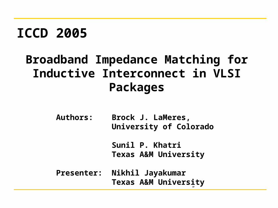
Problem Statement
• Reflections from interconnect will limit VLSI system performance
• This is caused by :
1) Inductive Package Interconnect
2) Faster Risetimes in Off-chip Driver Circuitry
October 5, 2005 “Broadband Impedance Matching” 3
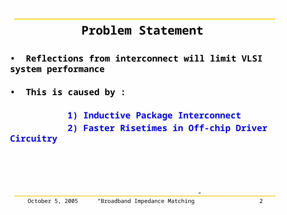
Agenda
1) Inductive Package Interconnect
2) Proposed Solution
3) Experimental Results
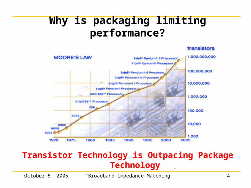
October 5, 2005 “Broadband Impedance Matching” 4
Why is packaging limiting performance?
Transistor Technology is Outpacing Package Technology
October 5, 2005 “Broadband Impedance Matching” 5
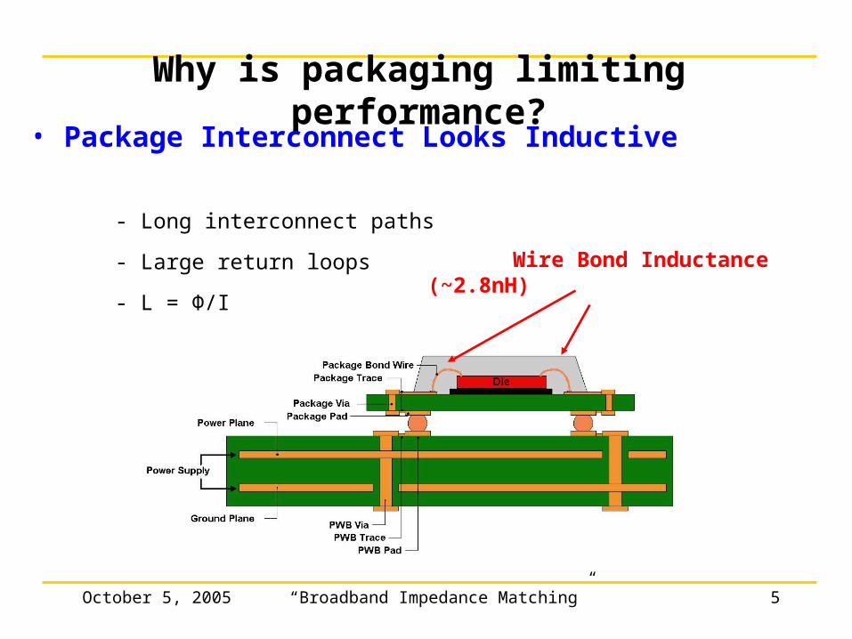
Why is packaging limiting performance?• Package Interconnect Looks Inductive
- Long interconnect paths
- Large return loops
- L = Φ/I
Wire Bond Inductance (~2.8nH)
October 5, 2005 “Broadband Impedance Matching” 6
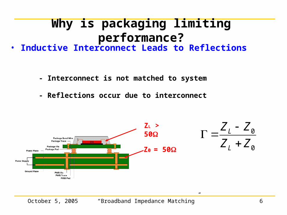
Why is packaging limiting performance?• Inductive Interconnect Leads to Reflections
- Interconnect is not matched to system
- Reflections occur due to interconnect
ZL > 500
0
L
L
Z Z
Z Z
Z0 = 50
October 5, 2005 “Broadband Impedance Matching” 7
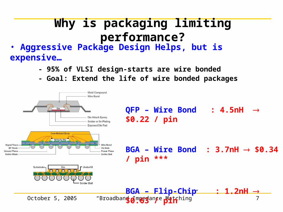
Why is packaging limiting performance?• Aggressive Package Design Helps, but is expensive…
- 95% of VLSI design-starts are wire bonded - Goal: Extend the life of wire bonded packages
QFP – Wire Bond : 4.5nH $0.22 / pin
BGA – Wire Bond : 3.7nH $0.34 / pin ***
BGA – Flip-Chip : 1.2nH $0.63 / pin
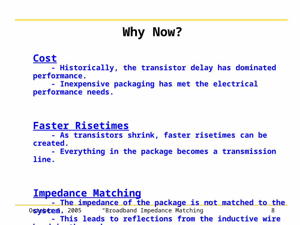
October 5, 2005 “Broadband Impedance Matching” 8
Why Now?
Cost - Historically, the transistor delay has dominated performance. - Inexpensive packaging has met the electrical performance needs.
Faster Risetimes - As transistors shrink, faster risetimes can be created. - Everything in the package becomes a transmission line.
Impedance Matching - The impedance of the package is not matched to the system. - This leads to reflections from the inductive wire bond in the package
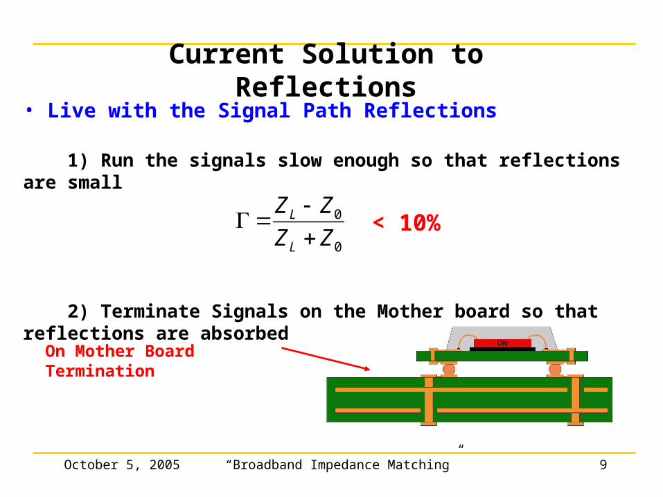
October 5, 2005 “Broadband Impedance Matching” 9
Current Solution to Reflections• Live with the Signal Path Reflections 1) Run the signals slow enough so that reflections are small
2) Terminate Signals on the Mother board so that reflections are absorbed
< 10%0
0
L
L
Z Z
Z Z
On Mother Board Termination
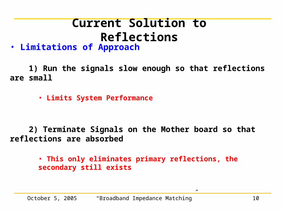
October 5, 2005 “Broadband Impedance Matching” 10
Current Solution to Reflections• Limitations of Approach 1) Run the signals slow enough so that reflections are small
• Limits System Performance
2) Terminate Signals on the Mother board so that reflections are absorbed
• This only eliminates primary reflections, the secondary still exists
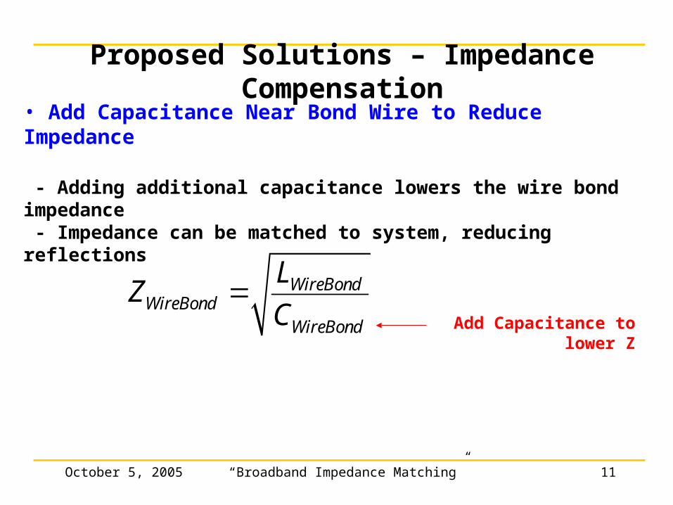
October 5, 2005 “Broadband Impedance Matching” 11
Proposed Solutions – Impedance Compensation• Add Capacitance Near Bond Wire to Reduce Impedance
- Adding additional capacitance lowers the wire bond impedance - Impedance can be matched to system, reducing reflections
WireBondWireBond
WireBond
LZ
C
Add Capacitance to lower Z
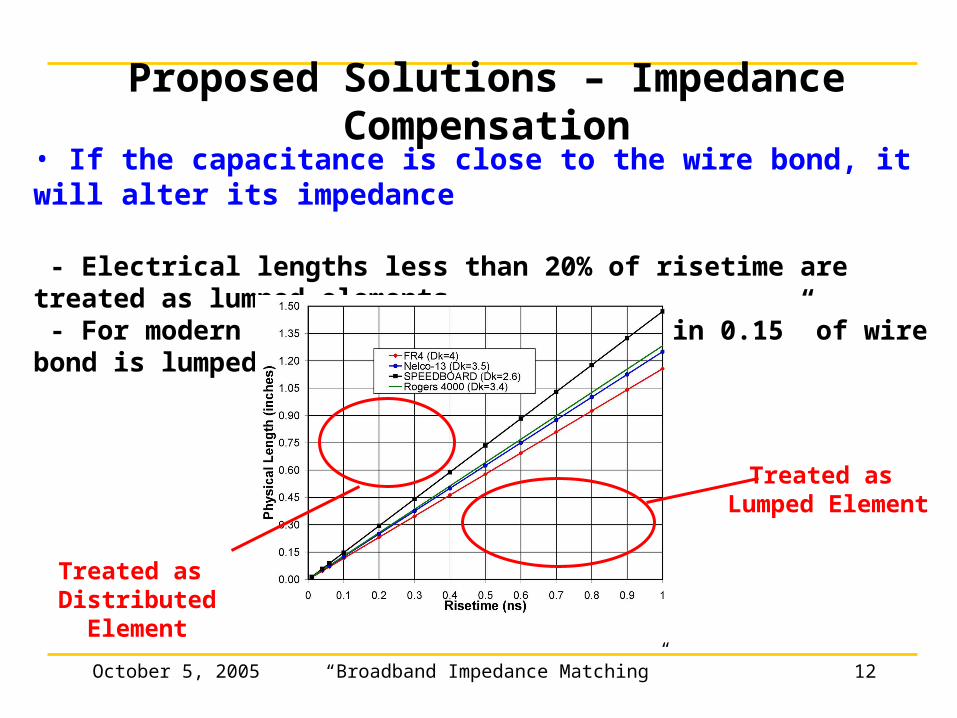
October 5, 2005 “Broadband Impedance Matching” 12
Proposed Solutions – Impedance Compensation• If the capacitance is close to the wire bond, it will alter its impedance
- Electrical lengths less than 20% of risetime are treated as lumped elements - For modern dielectrics, anything within 0.15” of wire bond is lumped
Treated as Lumped Element
Treated as Distributed Element
October 5, 2005 “Broadband Impedance Matching” 13
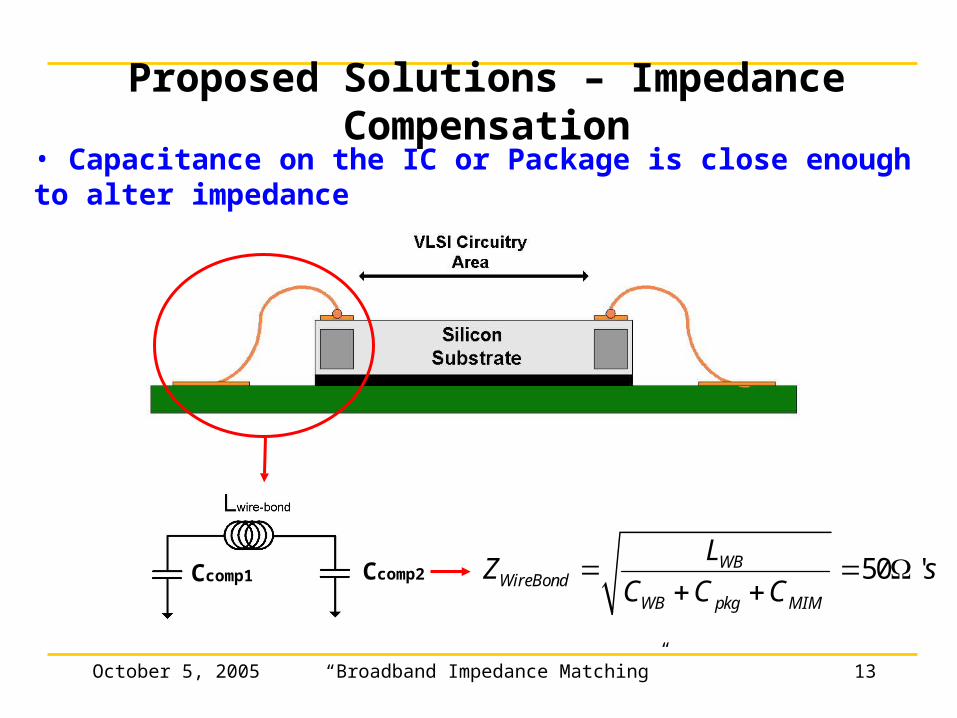
Proposed Solutions – Impedance Compensation• Capacitance on the IC or Package is close enough to alter impedance
Ccomp2Ccomp1 50 'WBWireBond
WB pkg MIM
LZ s
C C C
October 5, 2005 “Broadband Impedance Matching” 14
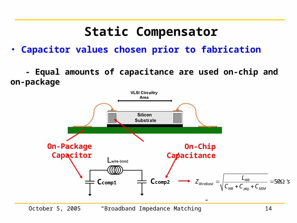
Ccomp2Ccomp1
Static Compensator• Capacitor values chosen prior to fabrication
- Equal amounts of capacitance are used on-chip and on-package
On-Package Capacitor On-Chip Capacitance
50 'WBWireBond
WB pkg MIM
LZ s
C C C
October 5, 2005 “Broadband Impedance Matching” 15
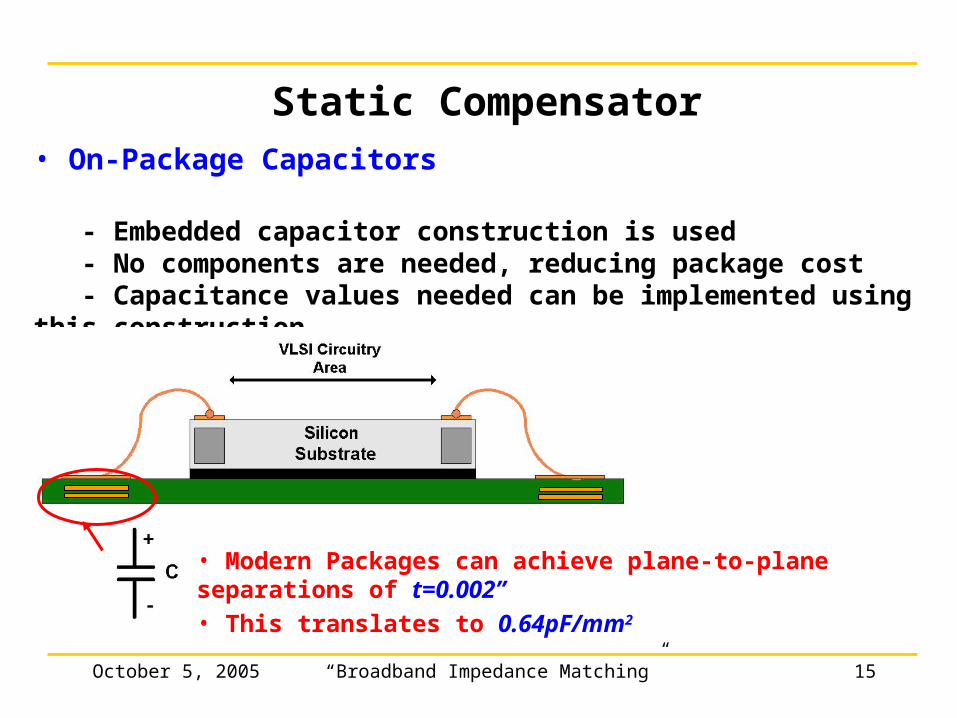
Static Compensator• On-Package Capacitors
- Embedded capacitor construction is used - No components are needed, reducing package cost - Capacitance values needed can be implemented using this construction
• Modern Packages can achieve plane-to-plane separations of t=0.002” • This translates to 0.64pF/mm2
October 5, 2005 “Broadband Impedance Matching” 16
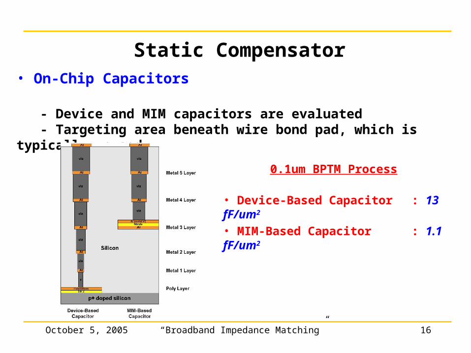
Static Compensator• On-Chip Capacitors
- Device and MIM capacitors are evaluated - Targeting area beneath wire bond pad, which is typically unused
0.1um BPTM Process
• Device-Based Capacitor : 13 fF/um2 • MIM-Based Capacitor : 1.1 fF/um2
October 5, 2005 “Broadband Impedance Matching” 17
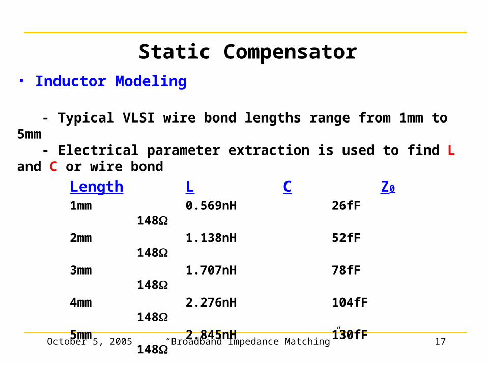
Static Compensator• Inductor Modeling
- Typical VLSI wire bond lengths range from 1mm to 5mm - Electrical parameter extraction is used to find L and C or wire bond
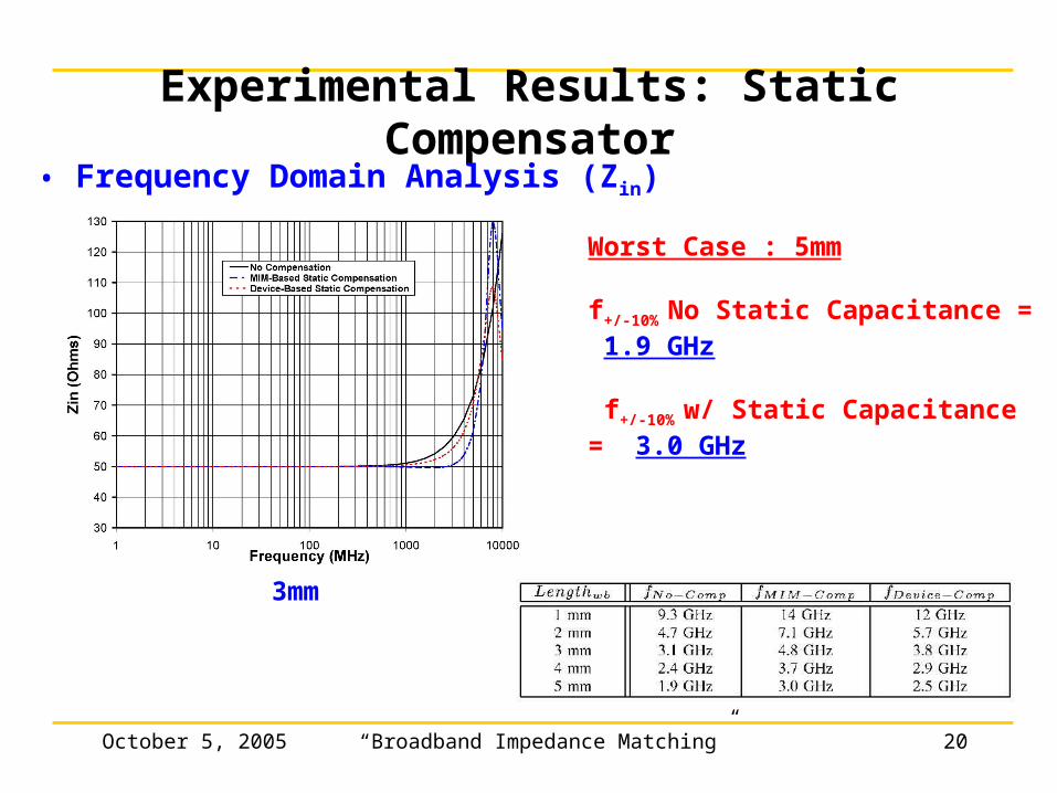
Length L C Z0
1mm 0.569nH 26fF 1482mm 1.138nH 52fF 1483mm 1.707nH 78fF 1484mm 2.276nH 104fF 1485mm 2.845nH 130fF 148
October 5, 2005 “Broadband Impedance Matching” 18
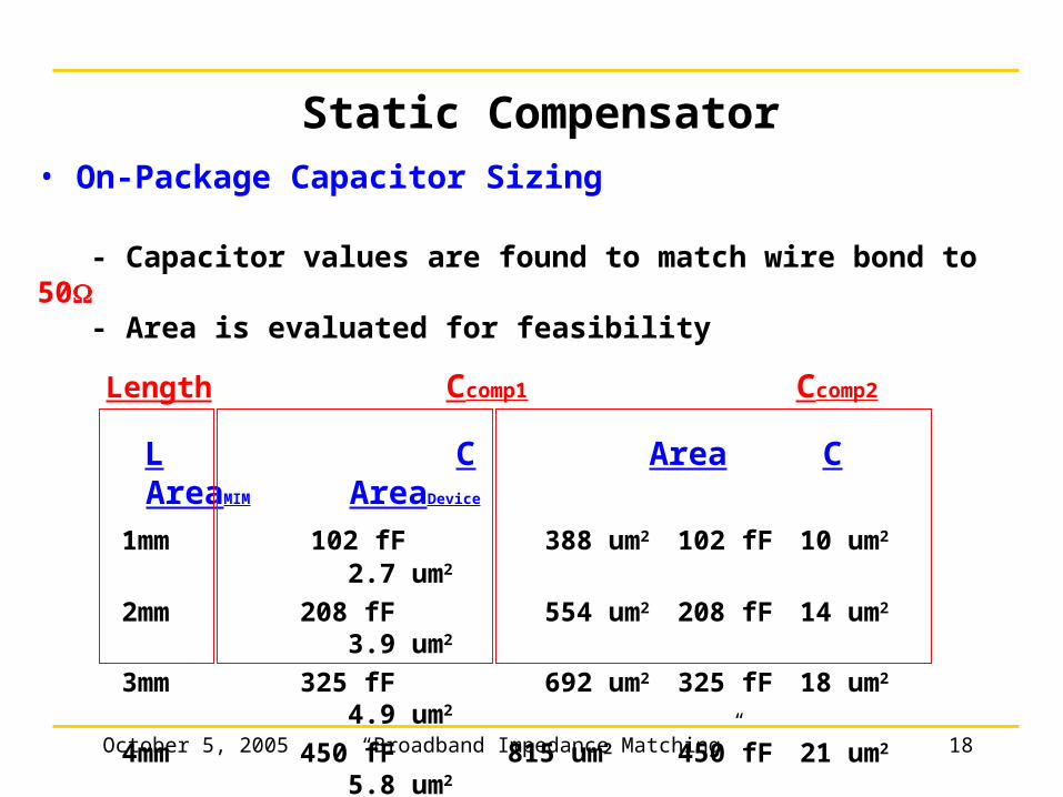
Static Compensator• On-Package Capacitor Sizing
- Capacitor values are found to match wire bond to 50 - Area is evaluated for feasibility
Length Ccomp1 Ccomp2
L C Area C AreaMIM AreaDevice
1mm 102 fF 388 um2 102 fF 10 um2 2.7 um2
2mm 208 fF 554 um2 208 fF 14 um2 3.9 um2
3mm 325 fF 692 um2 325 fF 18 um2 4.9 um2
4mm 450 fF 815 um2 450 fF 21 um2 5.8 um2
5mm 575 fF 921 um2 575 fF 24 um2 6.5 um2
October 5, 2005 “Broadband Impedance Matching” 19
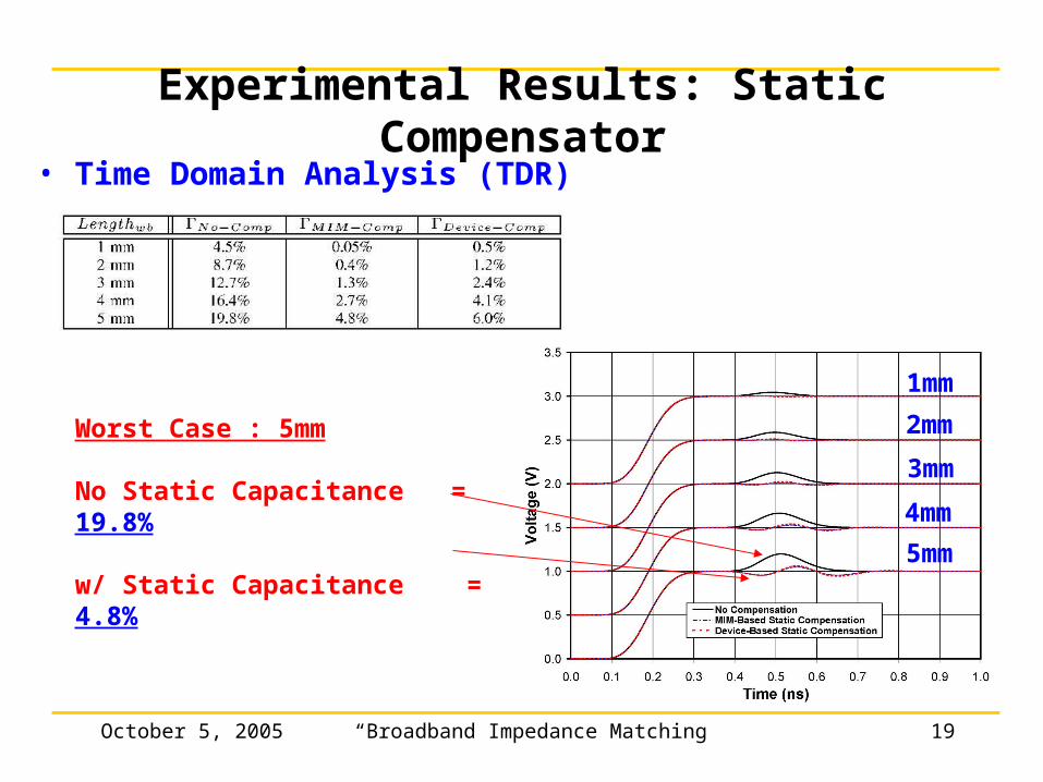
Worst Case : 5mm
No Static Capacitance = 19.8%
w/ Static Capacitance = 4.8%
Experimental Results: Static Compensator• Time Domain Analysis (TDR)
1mm
2mm
3mm
4mm
5mm
October 5, 2005 “Broadband Impedance Matching” 20
Worst Case : 5mm
f+/-10% No Static Capacitance = 1.9 GHz
f+/-10% w/ Static Capacitance = 3.0 GHz
Experimental Results: Static Compensator• Frequency Domain Analysis (Zin)
3mm
October 5, 2005 “Broadband Impedance Matching” 21
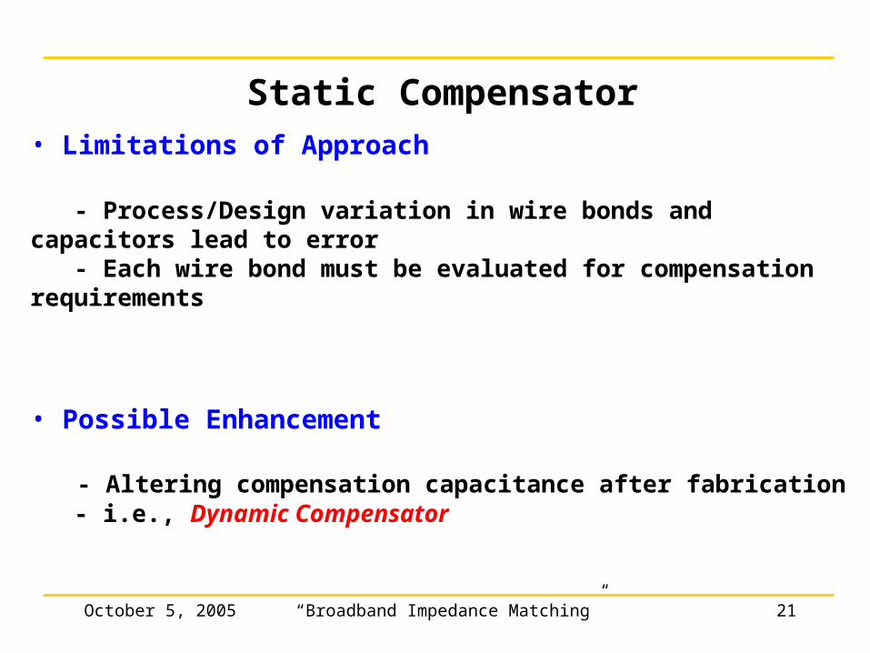
Static Compensator• Limitations of Approach
- Process/Design variation in wire bonds and capacitors lead to error - Each wire bond must be evaluated for compensation requirements
• Possible Enhancement
- Altering compensation capacitance after fabrication - i.e., Dynamic Compensator
October 5, 2005 “Broadband Impedance Matching” 22
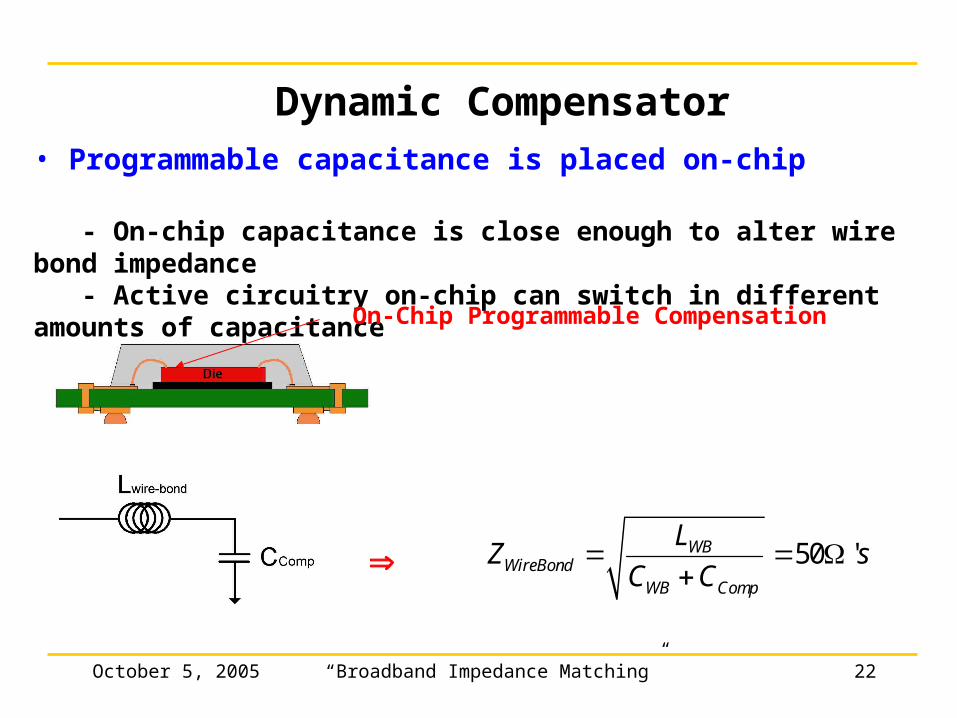
Dynamic Compensator• Programmable capacitance is placed on-chip
- On-chip capacitance is close enough to alter wire bond impedance - Active circuitry on-chip can switch in different amounts of capacitance
On-Chip Programmable Compensation
50 'WBWireBond
WB Comp
LZ s
C C
October 5, 2005 “Broadband Impedance Matching” 23
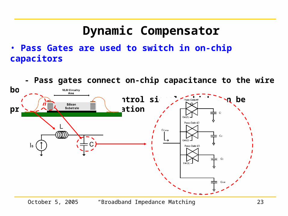
Dynamic Compensator• Pass Gates are used to switch in on-chip capacitors
- Pass gates connect on-chip capacitance to the wire bond inductance - Pass gates have control signals which can be programmed after fabrication
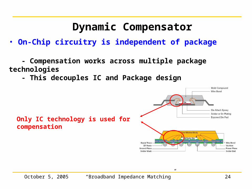
October 5, 2005 “Broadband Impedance Matching” 24
Dynamic Compensator• On-Chip circuitry is independent of package
- Compensation works across multiple package technologies - This decouples IC and Package design
Only IC technology is used for compensation
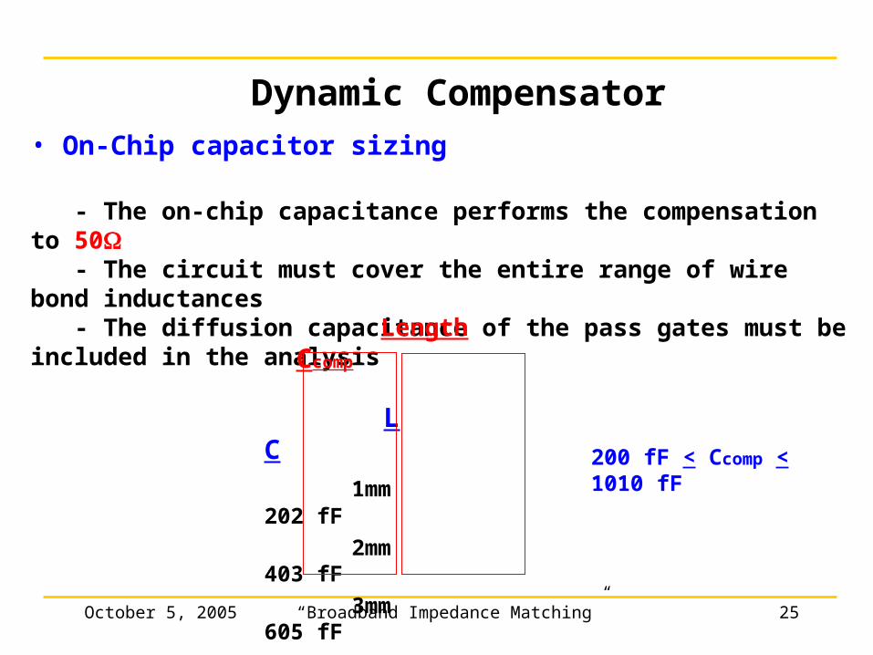
October 5, 2005 “Broadband Impedance Matching” 25
Dynamic Compensator• On-Chip capacitor sizing
- The on-chip capacitance performs the compensation to 50 - The circuit must cover the entire range of wire bond inductances - The diffusion capacitance of the pass gates must be included in the analysis
Length Ccomp
L C
1mm 202 fF
2mm 403 fF
3mm 605 fF
4mm 806 fF
5mm 1008 fF
200 fF < Ccomp < 1010 fF
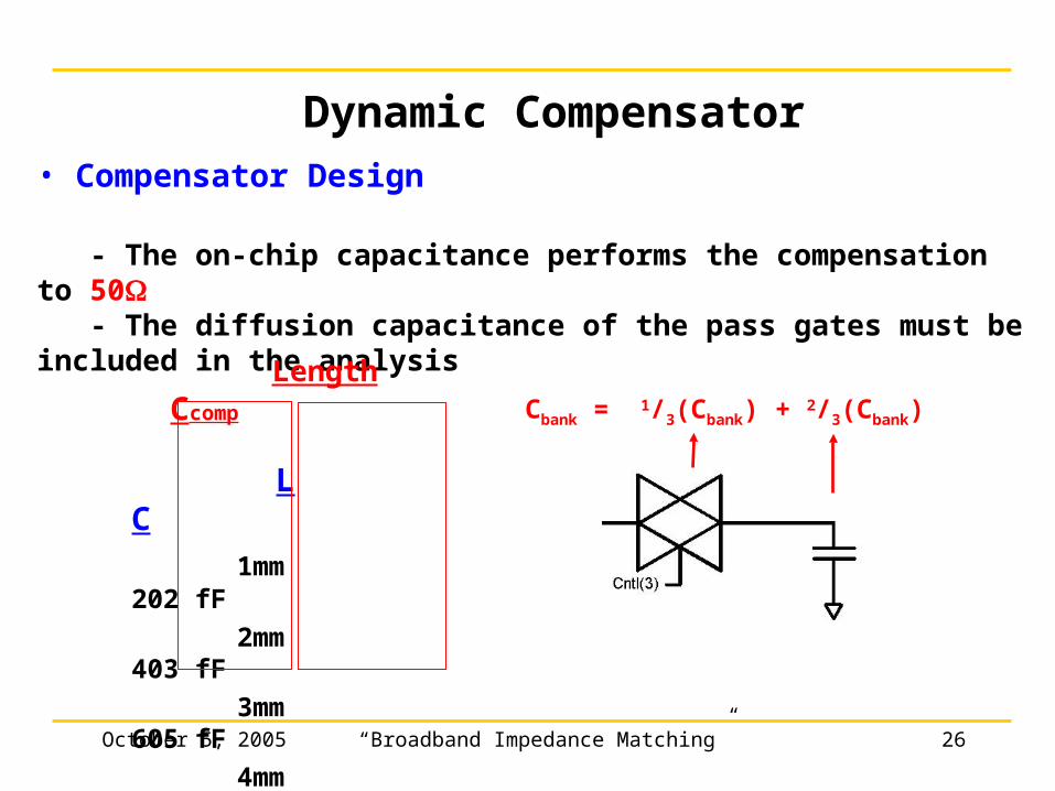
October 5, 2005 “Broadband Impedance Matching” 26
Dynamic Compensator• Compensator Design
- The on-chip capacitance performs the compensation to 50 - The diffusion capacitance of the pass gates must be included in the analysis
Length Ccomp
L C
1mm 202 fF
2mm 403 fF
3mm 605 fF
4mm 806 fF
5mm 1008 fF
Cbank = 1/3(Cbank) + 2/3(Cbank)
October 5, 2005 “Broadband Impedance Matching” 27
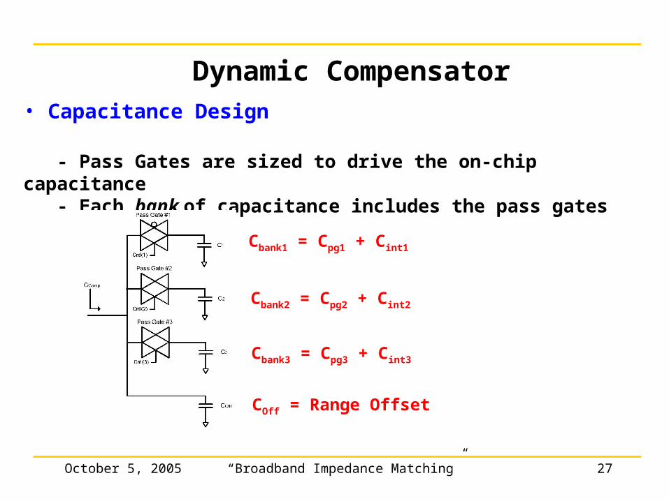
Dynamic Compensator• Capacitance Design
- Pass Gates are sized to drive the on-chip capacitance - Each bank of capacitance includes the pass gates
Cbank1 = Cpg1 + Cint1
Cbank2 = Cpg2 + Cint2
Cbank3 = Cpg3 + Cint3
COff = Range Offset
October 5, 2005 “Broadband Impedance Matching” 28
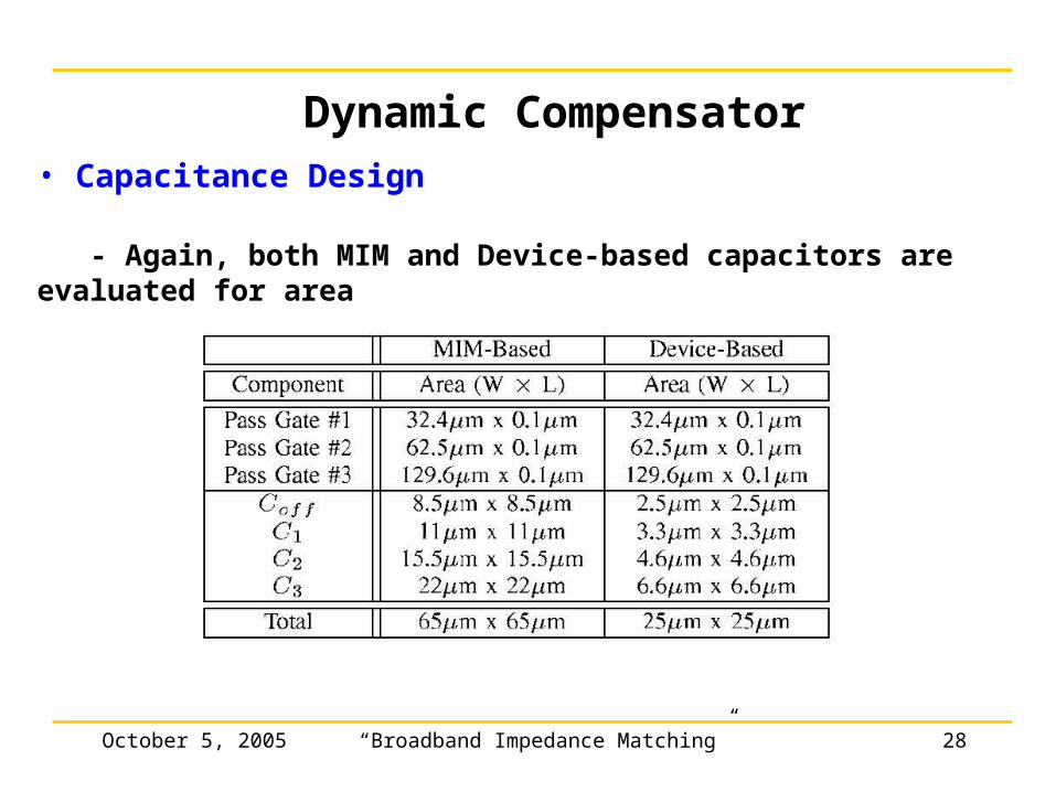
Dynamic Compensator• Capacitance Design
- Again, both MIM and Device-based capacitors are evaluated for area
October 5, 2005 “Broadband Impedance Matching” 29
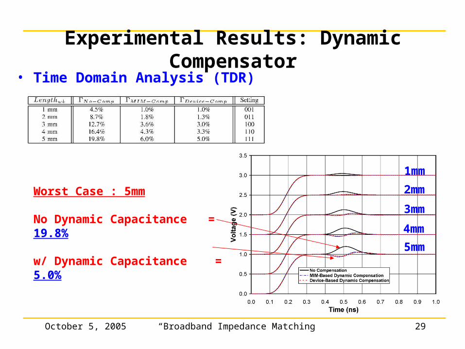
Worst Case : 5mm
No Dynamic Capacitance = 19.8%
w/ Dynamic Capacitance = 5.0%
Experimental Results: Dynamic Compensator• Time Domain Analysis (TDR)
1mm
2mm
3mm
4mm
5mm
October 5, 2005 “Broadband Impedance Matching” 30
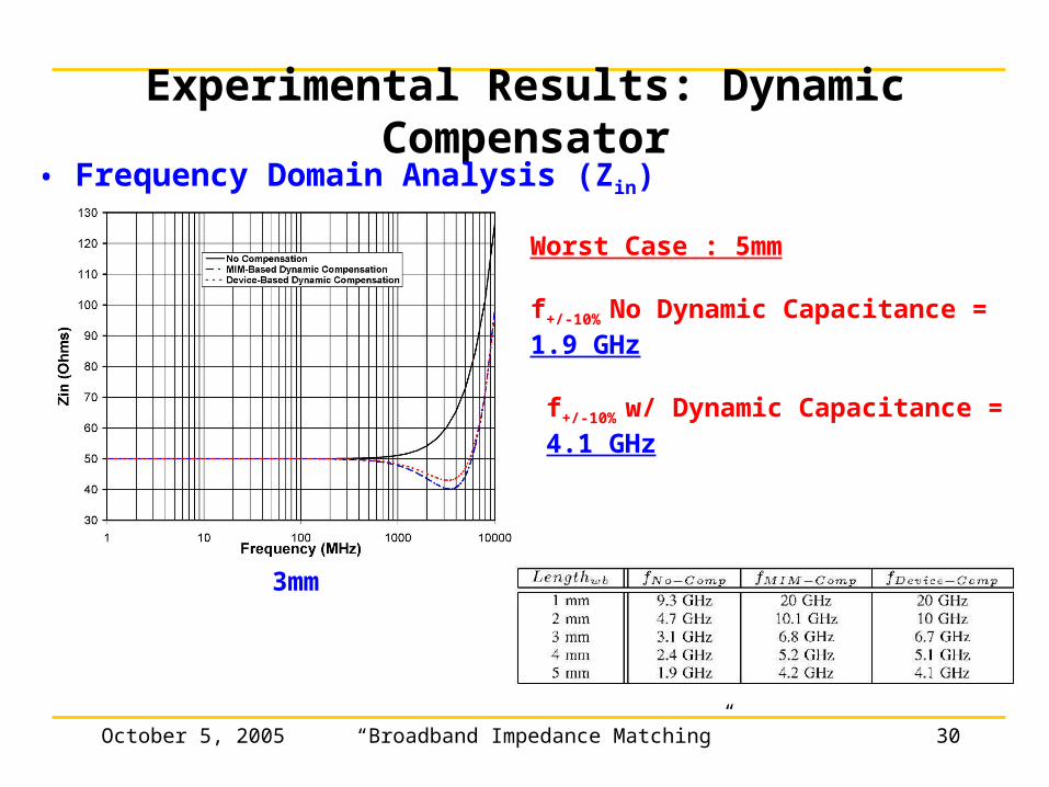
Worst Case : 5mm
f+/-10% No Dynamic Capacitance = 1.9 GHz
f+/-10% w/ Dynamic Capacitance = 4.1 GHz
Experimental Results: Dynamic Compensator• Frequency Domain Analysis (Zin)
3mm
October 5, 2005 “Broadband Impedance Matching” 31
Summary
• Inductive Package Interconnect causes reflections which limits system performance
• The move toward Advanced Packaging is Resisted due to Cost
• Adding On-Chip & On-Package capacitors does not add cost
• A Static and Dynamic Compensation Approach can match the package interconnect impedance to the system
October 5, 2005 “Broadband Impedance Matching” 32
Questions?


![Distributed Matching Network Design for Broadband Power ...livrepository.liverpool.ac.uk/3020523/1/EDAPS_Final[6833].pdf · B. Matching Network Design Method Once the optimal impedance](https://img.pdfslide.net/doc/110x75/6065a149f38fc267a6757d78/distributed-matching-network-design-for-broadband-power-6833pdf-b-matching.jpg)


![Matching Network Elimination in Broadband Rectennas for High … · rectennas. Thus in previous work [19] [24], the structures of the impedance matching networks were complex for](https://img.pdfslide.net/doc/110x75/60d541f11e8a1a043b412401/matching-network-elimination-in-broadband-rectennas-for-high-rectennas-thus-in.jpg)