Embed Size (px)
Citation preview

This is information on a product in full production.
August 2013 DocID14419 Rev 9 1/32
VIPER17
Off-line high voltage converters
Datasheet - production data
Figure 1. Typical topology
Features• 800 V avalanche rugged power section
• PWM operation with frequency jittering for low
EMI
• Operating frequency:
– 60 kHz for L type
– 115 kHz for H type
• Standby power < 50 mW at 265 Vac
• Limiting current with adjustable set point
• Adjustable and accurate overvoltage
protection
• On-board soft-start
• Safe auto-restart after a fault condition
• Hysteresis thermal shutdown
Application• Adapters for PDA, camcorders, shavers,
cellular phones, videogames
• Auxiliary power supply for LCD/PDP TV,
monitors, audio systems, computer, industrial
systems, LED driver, No el-cap LED driver
• SMPS for set-top boxes, DVD players and
recorders, white goods
DescriptionThe device is an off-line converter with an 800 V
rugged power section, a PWM control, two levels
of overcurrent protection, overvoltage and
overload protections, hysteresis thermal
protection, soft-start and safe auto-restart after
any fault condition removal. The burst mode
operation and the device’s very low consumption
meet the standby energy saving regulations.
Advance frequency jittering reduces EMI filter
cost. Brown-out function protects the switch mode
power supply when the rectified input voltage
level is below the normal minimum level specified
for the system. The high voltage start-up circuit is
embedded in the device.
SO-16DIP-7SO16 narrow
DC input high voltage wide range
-
+
DC Output voltage
-
+
VIPER17
DRAIN DRAIN BR
VDD CONT FBGND
Table 1. Device summary
Order codes Package Packaging
VIPER17LN / VIPER17HN DIP-7 Tube
VIPER17HD / VIPER17LD
SO16 narrow
Tube
VIPER17HDTR / VIPER17LDTR Tape and reel
www.st.com

Contents VIPER17
2/32 DocID14419 Rev 9
Contents
1 Block diagram . . . . . . . . . . . . . . . . . . . . . . . . . . . . . . . . . . . . . . . . . . . . . . 3
2 Typical power . . . . . . . . . . . . . . . . . . . . . . . . . . . . . . . . . . . . . . . . . . . . . . . 3
3 Pin settings . . . . . . . . . . . . . . . . . . . . . . . . . . . . . . . . . . . . . . . . . . . . . . . . 4
4 Electrical data . . . . . . . . . . . . . . . . . . . . . . . . . . . . . . . . . . . . . . . . . . . . . . 5
4.1 Maximum ratings . . . . . . . . . . . . . . . . . . . . . . . . . . . . . . . . . . . . . . . . . . . . 5
4.2 Thermal data . . . . . . . . . . . . . . . . . . . . . . . . . . . . . . . . . . . . . . . . . . . . . . . 5
4.3 Electrical characteristics . . . . . . . . . . . . . . . . . . . . . . . . . . . . . . . . . . . . . . . 6
5 Typical electrical characteristics . . . . . . . . . . . . . . . . . . . . . . . . . . . . . . 10
6 Typical circuit . . . . . . . . . . . . . . . . . . . . . . . . . . . . . . . . . . . . . . . . . . . . . 13
7 Operation descriptions . . . . . . . . . . . . . . . . . . . . . . . . . . . . . . . . . . . . . . 14
7.1 Power section and gate driver . . . . . . . . . . . . . . . . . . . . . . . . . . . . . . . . . 14
7.2 High voltage startup generator . . . . . . . . . . . . . . . . . . . . . . . . . . . . . . . . . 14
7.3 Power-up and soft-start up . . . . . . . . . . . . . . . . . . . . . . . . . . . . . . . . . . . . 14
7.4 Power down operation . . . . . . . . . . . . . . . . . . . . . . . . . . . . . . . . . . . . . . . 17
7.5 Auto restart operation . . . . . . . . . . . . . . . . . . . . . . . . . . . . . . . . . . . . . . . . 17
7.6 Oscillator . . . . . . . . . . . . . . . . . . . . . . . . . . . . . . . . . . . . . . . . . . . . . . . . . 18
7.7 Current mode conversion with adjustable current limit set point . . . . . . . 18
7.8 Overvoltage protection (OVP) . . . . . . . . . . . . . . . . . . . . . . . . . . . . . . . . . 18
7.9 About CONT pin . . . . . . . . . . . . . . . . . . . . . . . . . . . . . . . . . . . . . . . . . . . . 20
7.10 Feed-back and overload protection (OLP) . . . . . . . . . . . . . . . . . . . . . . . . 21
7.11 Burst-mode operation at no load or very light load . . . . . . . . . . . . . . . . . . 23
7.12 Brown-out protection . . . . . . . . . . . . . . . . . . . . . . . . . . . . . . . . . . . . . . . . 24
7.13 2nd level overcurrent protection and hiccup mode . . . . . . . . . . . . . . . . . . 26
8 Package mechanical data . . . . . . . . . . . . . . . . . . . . . . . . . . . . . . . . . . . . 27
9 Revision history . . . . . . . . . . . . . . . . . . . . . . . . . . . . . . . . . . . . . . . . . . . 31

DocID14419 Rev 9 3/32
VIPER17 Block diagram
32
1 Block diagram
2 Typical power
Figure 2. Block diagram
THERMALSHUTDOWN
6uA
LEB
&
OVPLOGIC
SOFTSTART OCP
BLOCK
Ref
TURN-ONLOGIC
DRAIN
SUPPLY& UVLO
OTPOLP
BURST
Internal Supply bus
BR
BURST-MODELOGIC
BURST
S
R1 R2
Q
-
+
UVLO
Vin_OK
+
- OCP
Ref erence Voltages
OVP
15uA
IDDch
OVP
Vcc
OSCILLATOR
FB
VBRth
HV_ON
OTP
.
GND
+
-
Rsense
CONT
+
-
PWM
2nd OCPLOGIC
VDD
Table 2. Typical power
Part number230 VAC 85-265 VAC
Adapter(1) Open frame(2) Adapter(1) Open frame(2)
VIPER17 9 W 10 W 5 W 6 W
1. Typical continuous power in non ventilated enclosed adapter measured at 50 °C ambient.
2. Maximum practical continuous power in an open frame design at 50 °C ambient, with adequate heat sinking.

Pin settings VIPER17
4/32 DocID14419 Rev 9
3 Pin settings
Figure 3. Connection diagram (top view)
Note: The copper area for heat dissipation has to be designed under the DRAIN pins.
Table 3. Pin description
Pin N.Name Function
DIP-7 SO16
1 1...2 GND This pin represents the device ground and the source of the power section.
- 4 N.A.
Not available for user. It can be connected to GND (pins 1-2) or left not
connected.
2 5 VDD
Supply voltage of the control section. This pin also provides the charging current
of the external capacitor during start-up time.
3 6 CONT
Control pin. The following functions can be selected:
1. current limit set point adjustment. The internal set default value of the cycle-
by-cycle current limit can be reduced by connecting to ground an external
resistor.
2. output voltage monitoring. A voltage exceeding VOVP
threshold (see Table 8)
shuts the IC down reducing the device consumption. This function is strobed and
digitally filtered for high noise immunity.
4 7 FB
Control input for duty cycle control. Internal current generator provides bias
current for loop regulation. A voltage below the threshold VFBbm
activates the
burst-mode operation. A level close to the threshold VFBlin
means that we are
approaching the cycle-by-cycle over-current set point.
5 10 BR
Brownout protection input with hysteresis. A voltage below the threshold VBRth
shuts down (not latch) the device and lowers the power consumption. Device
operation restarts as the voltage exceeds the threshold VBRth
+ VBRhyst
.
It can be connected to ground when not used.
7,8 13...16 DRAIN
High voltage drain pin. The built-in high voltage switched start-up bias current is
drawn from this pin too. Pins connected to the metal frame to facilitate heat
dissipation.

DocID14419 Rev 9 5/32
VIPER17 Electrical data
32
4 Electrical data
4.1 Maximum ratings
4.2 Thermal data
Table 4. Absolute maximum ratings
SymbolPin
(DIP7)Parameter
ValueUnit
Min Max
VDRAIN
7, 8 Drain-to-source (ground) voltage 800 V
EAV
7, 8
Repetitive avalanche energy
(limited by TJ
= 150 °C)
2 mJ
IAR
7, 8
Repetitive avalanche current
(limited by TJ = 150 °C)
1 A
IDRAIN
7, 8 Pulse drain current 2.5 A
VCONT
3 Control input pin voltage (with ICONT
= 1 mA) -0.3 Self limited V
VFB
4 Feed-back voltage -0.3 5.5 V
VBR
5 Brown-out input pin voltage (with IBR
= 0.5 mA) -0.3 Self limited V
VDD
2 Supply voltage (IDD
= 25 mA) -0.3 Self limited V
IDD
2 Input current 25 mA
PTOT
Power dissipation at TA < 40 °C (DIP-7) 1 W
Power dissipation at TA < 60 °C (SO16N) 1 W
TJ
Operating junction temperature range -40 150 °C
TSTG
Storage temperature -55 150 °C
Table 5. Thermal data
Symbol ParameterMax value
SO16N
Max value
DIP7Unit
RthJP
Thermal resistance junction pin
(Dissipated power = 1 W)
35 40 °C/W
RthJA
Thermal resistance junction ambient
(Dissipated power = 1 W)
90 110 °C/W
RthJA
Thermal resistance junction ambient (1)
(Dissipated power = 1 W)
1. When mounted on a standard single side FR4 board with 100 mm2 (0.155 sq in) of Cu (35 μm thick)
80 90 °C/W

Electrical data VIPER17
6/32 DocID14419 Rev 9
4.3 Electrical characteristics (T
J = -25 to 125 °C, V
DD = 14 V
(a); unless otherwise specified)
a. Adjust VDD
above VDDon
start-up threshold before settings to 14 V.
Table 6. Power section
Symbol Parameter Test condition Min Typ Max Unit
VBVDSS
Break-down voltage
IDRAIN
= 1 mA, VFB
= GND
TJ = 25 °C
800 V
IOFF
OFF state drain current
VDRAIN
= max rating,
VFB
= GND
60 μA
RDS(on)
Drain-source on state resistance
IDRAIN
= 0.2 A, VFB
= 3 V, VBR
=
GND, TJ = 25 °C
20 24 Ω
IDRAIN
= 0.2 A, VFB
= 3 V,
VBR
= GND, TJ = 125 °C
40 48 Ω
COSS
Effective (energy related) output
capacitance
VDRAIN
= 0 to 640 V 10 pF
Table 7. Supply section
Symbol Parameter Test condition Min Typ Max Unit
Voltage
VDRAIN_START
Drain-source start voltage 60 80 100 V
IDDch
Start up charging current
VDRAIN
= 120 V, VBR
= GND,
VFB
= GND, VDD
= 4 V
-2 -3 -4 mA
VDRAIN
= 120 V, VBR
= GND,
VFB
= GND, VDD
= 4 V after fault.
-0.4 -0.6 -0.8 mA
VDD
Operating voltage range After turn-on 8.5 23.5 V
VDDclamp
VDD
clamp voltage IDD
= 20 mA 23.5 V
VDDon
VDD
start up threshold
VDRAIN
= 120 V,
VBR
= GND, VFB
= GND
13 14 15 V
VDDoff
VDD
under voltage shutdown
threshold
7.5 8 8.5 V
VDD(RESTART)
VDD
restart voltage threshold
VDRAIN
= 120 V,
VBR
= GND, VFB
= GND
4 4.5 5 V
Current
IDD0
Operating supply current, not
switching
VFB
= GND, FSW
= 0 kHz, VBR
= GND,
VDD
= 10 V
0.9 mA
IDD1
Operating supply current, switching
VDRAIN
= 120 V, FSW
= 60 kHz 1.8 mA
VDRAIN
= 120 V, FSW
= 115 kHz 2 mA
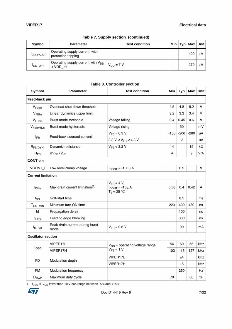
DocID14419 Rev 9 7/32
VIPER17 Electrical data
32
IDD_FAULT
Operating supply current, with
protection tripping
400 μA
IDD_OFF
Operating supply current with VDD
< VDD_off
VDD
= 7 V 270 μA
Table 7. Supply section (continued)
Symbol Parameter Test condition Min Typ Max Unit
Table 8. Controller section
Symbol Parameter Test condition Min Typ Max Unit
Feed-back pin
VFBolp
Overload shut down threshold 4.5 4.8 5.2 V
VFBlin
Linear dynamics upper limit 3.2 3.3 3.4 V
VFBbm
Burst mode threshold Voltage falling 0.4 0.45 0.6 V
VFBbmhys
Burst mode hysteresis Voltage rising 50 mV
IFB
Feed-back sourced current
VFB
= 0.3 V -150 -200 -280 uA
3.3 V < VFB
< 4.8 V -3 uA
RFB(DYN)
Dynamic resistance VFB
< 3.3 V 14 19 kΩ
HFB
∆VFB
/ ∆ID
4 9 V/A
CONT pin
VCONT_l Low level clamp voltage ICONT
= -100 μA 0.5 V
Current limitation
IDlim
Max drain current limitation(1)
VFB
= 4 V,
ICONT
= -10 μA
TJ = 25 °C
0.38 0.4 0.42 A
tSS
Soft-start time 8.5 ms
TON_MIN
Minimum turn ON time 220 400 480 ns
td Propagation delay 100 ns
tLEB
Leading edge blanking 300 ns
ID_BM
Peak drain current during burst
mode
VFB
= 0.6 V 90 mA
Oscillator section
FOSC
VIPER17LV
DD = operating voltage range,
VFB
= 1 V
54 60 66 kHz
VIPER17H 103 115 127 kHz
FD Modulation depth
VIPER17L ±4 kHz
VIPER17H ±8 kHz
FM Modulation frequency 250 Hz
DMAX
Maximum duty cycle 70 80 %
1. IDlim
@ VDD
lower than 10 V can range between -5% and +15%.

Electrical data VIPER17
8/32 DocID14419 Rev 9
Table 9. Controller section (continued)
Symbol Parameter Test condition Min Typ Max Unit
Overcurrent protection (2nd OCP)
IDMAX
Second over current threshold 0.6 A
Overvoltage protection
VOVP
Overvoltage protection threshold 2.7 3 3.3 V
TSTROBE
Overvoltage protection strobe time 2.2 μs
Brown out protection
VBRth
Brown out threshold Voltage falling 0.41 0.45 0.49 V
VBRhyst
Voltage hysteresis above VBRth
Voltage rising 50 mV
IBRhyst
Current hysteresis 7 12 μA
VBRclamp
Clamp voltage IBR
= 250 μA 3 V
VDIS
Brown out disable voltage 50 150 mV
Thermal shutdown
TSD
Thermal shutdown temperature 150 160 °C
THYST
Thermal shutdown hysteresis 30 °C

DocID14419 Rev 9 9/32
VIPER17 Electrical data
32
Figure 4. Minimum turn-on time test circuit
Figure 5. Brown out threshold test circuit
Figure 6. OVP threshold test circuit
Note: Adjust VDD above VDDon start-up threshold before settings to 14 V
14 V
3.5 V
50 Ω
30 V
GND
CONT
FB
VDD
DRAIN
BR
DRAIN
VDRAIN
IDRAIN
IDLIM
Time
Time
TONmin
90 %
10 %
GND
CONT
FB
VDD
DRAIN
BR
DRAIN
14 V
2 V
10 kΩ
30 V
IBRhyst
VBRth+VBRhystVBRth
VBR
IBR
VDIS
IBRhyst
IDRAIN
Time
Time
Time
GND
CONT
FB
VDD
DRAIN
BR
DRAIN
VOVP
VCONT
VDRAIN
14 V
2 V
10 kΩ
30 V
Time
Time

Typical electrical characteristics VIPER17
10/32 DocID14419 Rev 9
5 Typical electrical characteristics
Figure 7. Current limit vs TJ Figure 8. Switching frequency vs TJ
Figure 9. Drain start voltage vs TJ Figure 10. HFB vs TJ
Figure 11. Brown out threshold vs TJ Figure 12. Brown out hysteresis vs TJ

DocID14419 Rev 9 11/32
VIPER17 Typical electrical characteristics
32
Figure 13. Brown out hysteresis current vs TJ
Figure 14. Operating supply current(no switching) vs TJ
Figure 15. Operating supply current (switching) vs TJ
Figure 16. current limit vs RLIM
Figure 17. Power MOSFET on-resistance vs TJ
Figure 18. Power MOSFET break down voltage vs TJ

Typical electrical characteristics VIPER17
12/32 DocID14419 Rev 9
Figure 19. Thermal shutdown
TJ
VDD
IDRAIN
VDDon
time
VDDoff
VDD(RESTART)
TSD
time
time
TSD
- THYST
Shut down after over temperatureNormal operation Normal operation

DocID14419 Rev 9 13/32
VIPER17 Typical circuit
32
6 Typical circuit
Figure 20. Min-features flyback application
Figure 21. Full-features flyback application
OPTO
R5
C6
AC IN
R3
AC IN
VoutD3
R1
C5
U2
R4
BR
C4 R6
C3
C1
D1
GND
C2
R2 D2
BR
CONT
DRAIN
SOURCE
CONTROL
Vcc
FB
VDD
GND
BR
CONT
DRAIN
SOURCE
CONTROL
Vcc
FB
C3
C2BR
Vout
R2
Daux
C5
GND
Rl
R3
Rov p
Rh
Rlim
R6
D2
U2
AC IN
D3
R1
C6
OPTO
D1
C4
R5
AC IN
C1
R4
VDD
GND
Operation descriptions VIPER17
14/32 DocID14419 Rev 9
7 Operation descriptions
VIPER17 is a high-performance low-voltage PWM controller chip with an 800 V, avalanche
rugged power section.
The controller includes: the oscillator with jittering feature, the start up circuits with soft-start
feature, the PWM logic, the current limit circuit with adjustable set point, the second over
current circuit, the burst mode management, the brown-out circuit, the UVLO circuit, the
auto-restart circuit and the thermal protection circuit.
The current limit set-point is set by the CONT pin. The burst mode operation guaranties high
performance in the stand-by mode and helps in the energy saving norm accomplishment.
All the fault protections are built in auto restart mode with very low repetition rate to prevent
IC's over heating.
7.1 Power section and gate driverThe power section is implemented with an avalanche ruggedness N-channel MOSFET,
which guarantees safe operation within the specified energy rating as well as high dv/dt
capability. The power section has a BVDSS
of 800 V min. and a typical RDS(on)
of 20 Ω at 25 °C.
The integrated SenseFET structure allows a virtually loss-less current sensing.
The gate driver is designed to supply a controlled gate current during both turn-on and turn-
off in order to minimize common mode EMI. Under UVLO conditions an internal pull-down
circuit holds the gate low in order to ensure that the Power section cannot be turned on
accidentally.
7.2 High voltage startup generator The HV current generator is supplied through the DRAIN pin and it is enabled only if the
input bulk capacitor voltage is higher than VDRAIN_START
threshold, 80 VDC
typically. When
the HV current generator is ON, the IDDch
current (3 mA typical value) is delivered to the
capacitor on the VDD
pin. In case of auto restart mode after a fault event, the IDDch
current is
reduced to 0.6 mA, in order to have a slow duty cycle during the restart phase.
7.3 Power-up and soft-start upIf the input voltage rises up till the device start threshold, V
DRAIN_START, the V
DD voltage
begins to grow due to the IDDch
current (see Table 7 on page 6) coming from the internal
high voltage start up circuit. If the VDD
voltage reaches VDDon
threshold (see Table 7 on page 6) the power MOSFET starts switching and the HV current generator is turned OFF.
See Figure 23 on page 16.
The IC is powered by the energy stored in the capacitor on the VDD pin, CVDD
, until when
the self-supply circuit (typically an auxiliary winding of the transformer and a steering diode)
develops a voltage high enough to sustain the operation.

DocID14419 Rev 9 15/32
VIPER17 Operation descriptions
32
CVDD
capacitor must be sized enough to avoid fast discharge and keep the needed voltage
value higher than VDDoff
threshold. In fact, a too low capacitance value could terminate the
switching operation before the controller receives any energy from the auxiliary winding.
The following formula can be used for the VDD
capacitor calculation:
Equation 1
The tSSaux
is the time needed for the steady state of the auxiliary voltage. This time is
estimated by applicator according to the output stage configurations (transformer, output
capacitances, etc.).
During the converter start up time, the drain current limitation is progressively increased to
the maximum value. In this way the stress on the secondary diode is considerably reduced.
It also helps to prevent transformer saturation. The soft-start time lasts 8.5 ms and the
feature is implemented for every attempt of start up converter or after a fault.
Figure 22. IDD current during start-up and burst mode
CVDD
IDDch
tSSaux
×V
DDonV
DDoff–
----------------------------------------=
BURST MODENORMAL MODESTART- UP NORMAL MODE
IDDch
(-3 mA)
IDD1
IDD0
IDD
VFBbm
VFB
VDRAIN
VFBbmhys
VFBlin
VFBolp
VDD
VDDoff
VDDon
t
t
t
t

Operation descriptions VIPER17
16/32 DocID14419 Rev 9
Figure 23. Timing diagram: normal power-up and power-down sequences
Figure 24. Soft-start: timing diagram
IDD
VDD
VDRAIN
VDDon
time
VIN
VDRAIN_START
Power-on Power-off Normal operation
regulation is lost here
VIN
< VDRAIN_START
HV startup is no more activated
VDDoff
VDD(RESTART)
IDDch
(3mA)
time
time
time
tSS ( SOFT START- UP ) STEADY STATE
VFB
VFBlin
VFBolp
IDRAIN
IDlim
VOUT
DELAY (OLP)
t
t
t

DocID14419 Rev 9 17/32
VIPER17 Operation descriptions
32
7.4 Power down operation At converter power down, the system loses regulation as soon as the input voltage is so low
that the peak current limitation is reached. The VDD
voltage drops and when it falls below
the VDDoff
threshold (see Table 7 on page 6) the power MOSFET is switched OFF, the
energy transfers to the IC interrupted and consequently the VDD
voltages decreases,
Figure 23 on page 16. Later, if the VIN
is lower than VDRAIN_START
(see Table 7 on page 6),
the start up sequence is inhibited and the power down completed. This feature is useful to
prevent converter’s restart attempts and ensures monotonic output voltage decay during the
system power down.
7.5 Auto restart operation If after a converter power down, the V
IN is higher than V
DRAIN_START, the start up sequence
is not inhibited and will be activated only when the VDD
voltage drops down the
VDD(RESTART)
threshold (see Table 7 on page 6). This means that the HV start up current
generator restarts the VDD
capacitor charging only when the VDD
voltage drops below
VDD(RESTART)
. The scenario above described is for instance a power down because of a
fault condition. After a fault condition, the charging current, IDDch
, is 0.6 mA (typ.) instead of
the 3 mA (typ.) of a normal start up converter phase. This feature together with the low
VDD(RESTART)
threshold ensures that, after a fault, the restart attempts of the IC has a very
long repetition rate and the converter works safely with extremely low power throughput.
The Figure 25 shows the IC behavioral after a short circuit event.
Figure 25. Timing diagram: behavior after short circuit

Operation descriptions VIPER17
18/32 DocID14419 Rev 9
7.6 Oscillator The switching frequency is internally fixed to 60 kHz or 115 kHz. In both case the switching
frequency is modulated by approximately ±4 kHz (60 kHz version) or ±8 kHz
(115 kHz version) at 250 Hz (typical) rate, so that the resulting spread-spectrum action
distributes the energy of each harmonic of the switching frequency over a number of side-
band harmonics having the same energy on the whole but smaller amplitudes.
7.7 Current mode conversion with adjustable current limit set point The device is a current mode converter: the drain current is sensed and converted in
voltage that is applied to the non inverting pin of the PWM comparator. This voltage is
compared with the one on the feed-back pin through a voltage divider on cycle by cycle
basis.
The VIPER17 has a default current limit value, IDLIM
, that the designer can adjust according
the electrical specification, by the RLIM
resistor connected to the CONT see Figure 16 on page 11.
The CONT pin has a minimum current sunk needed to activate the IDLIM
adjustment: without
RLIM
or with high RLIM
(i.e. 100 KΩ) the current limit is fixed to the default value (see IDLIM
,
Table 8 on page 7).
7.8 Overvoltage protection (OVP)The VIPER17 has integrated the logic for the monitor of the output voltage using as input
signal the voltage VCONT
during the OFF time of the power MOSFET. This is the time when
the voltage from the auxiliary winding tracks the output voltage, through the turn ratio
The CONT pin has to be connected to the auxiliary winding through the diode DOVP
and the
resistors ROVP
and RLIM
as shows the Figure 27 on page 20 When, during the OFF time,
the voltage VCONT
exceeds, four consecutive times, the reference voltage VOVP
(see
Table 8 on page 7) the overvoltage protection will stop the power MOSFET and the
converter enters the auto-restart mode.
In order to bypass the noise immediately after the turn off of the power MOSFET, the voltage
VCONT
is sampled inside a short window after the time TSTROBE
, see Table 8 on page 7 and
the Figure 26 on page 20. The sampled signal, if higher than VOVP
, trigger the internal OVP
digital signal and increments the internal counter. The same counter is reset every time the
signal OVP is not triggered in one oscillator cycle.
Referring to the Figure 21, the resistors divider ratio kOVP
will be given by:
NAUX
NSEC
--------------

DocID14419 Rev 9 19/32
VIPER17 Operation descriptions
32
Equation 2
Equation 3
Where:
• VOVP
is the OVP threshold (see Table 9 on page 8)
• VOUT OVP
is the converter output voltage value to activate the OVP (set by designer)
• NAUX
is the auxiliary winding turns
• NSEC
is the secondary winding turns
• VDSEC
is the secondary diode forward voltage
• VDAUX
is the auxiliary diode forward voltage
• ROVP
together RLIM
make the output voltage divider
Than, fixed RLIM,
according to the desired IDLIM
, the ROVP
can be calculating by:
Equation 4
The resistor values will be such that the current sourced and sunk by the CONT pin be
within the rated capability of the internal clamp.
kOVP
VOVP
NAUX
NSEC
-------------- VOUTOVP
VDSEC
+( ) VDAUX
–⋅---------------------------------------------------------------------------------------------------=
kOVP
RLIM
RLIM
ROVP
+----------------------------------=
ROVP
RLIM
1 kOVP
–
kOVP
-----------------------×=

Operation descriptions VIPER17
20/32 DocID14419 Rev 9
Figure 26. OVP timing diagram
7.9 About CONT pinReferring to the Figure 27, through the CONT pin, the below features can be implemented:
1. Current Limit set point
2. Over voltage protection on the converter output voltage
The Table 10 on page 21 referring to the Figure 27, lists the external components needed to
activate one or plus of the CONT pin functions.
Figure 27. CONT pin configuration
tVAUX
t
t
t
STROBE
t
COUNTERRESET
t
COUNTERSTATUS
t
0 VCONT
2 µs 0.5 µs
OVP
FAULT
0 0 0 0 →1 1 →2 2 →0 0 →1 1 → 2 2 →3 3 → 40
ERULIAF POOL KCABDEEFECNABRUTSID YRAROPMETNOITAREPO LAMRONt
VOVP t
t
t
STROBE
t
COUNTERRESET
t
COUNTERSTATUS
t
0
2 µs 0.5 µs
OVP
FAULT
0 0 0 0 →1 1 →2 2 →0 0 →1 1 → 2 2 →3 3 → 40
ERULIAF POOL KCABDEEFECNABRUTSID YRAROPMETNOITAREPO LAMRONt
+
-
OVP
ROV PSOFT
STARTCONTDaux
RLIMFrom RSENSE
Auxiliarywinding
to GATE driver
OVP LOGIC
OCPBLOCK OCP

DocID14419 Rev 9 21/32
VIPER17 Operation descriptions
32
7.10 Feed-back and overload protection (OLP)The VIPER17 is a current mode converter: the feedback pin controls the PWM operation,
controls the burst mode and actives the overload protection. Figure 28 on page 23 and
Figure 29 show the internal current mode structure.
With the feedback pin voltage between VFBbm
and VFBlin
, see Table 8 on page 7, the drain
current is sensed and converted in voltage that is applied to the non inverting pin of the
PWM comparator. See Figure 2 on page 3.
This voltage is compared with the one on the feedback pin through a voltage divider on
cycle by cycle basis. When these two voltages are equal, the PWM logic orders the switch
off of the power MOSFET. The drain current is always limited to IDlim
value.
In case of overload the feedback pin increases in reaction to this event and when it goes
higher than VFBlin
, the PWM comparator is disabled and the drain current is limited to IDlim
by
the OCP comparator, seeFigure 2 on page 3.
When the feedback pin voltage reaches the threshold VFBlin
an internal current generator
starts to charge the feedback capacitor (CFB
) and when the feedback voltage reaches the
VFBolp
threshold, the converter is turned off and the start up phase is activated with reduced
value of IDDch
to 0.6 mA. See Table 7 on page 6.
During the first start up phase of the converter, after the soft-start up time, tSS
, the output
voltage could force the feedback pin voltage to rise up to the VFBolp
threshold that switches
off the converter itself.
To avoid this event, the appropriate feedback network has to be selected according to the
output load. More the network feedback fixes the compensation loop stability. The Figure 28 on page 23 and Figure 29 show the two different feedback networks.
The time from the over load detection (VFB
= VFBlin
) to the device shutdown
(VFB
= VFBolp
) can be calculating by CFB
value (see Figure 28 on page 23 and Figure 29),
using the formula:
Equation 5
In the Figure 28, the capacitor connected to FB pin (CFB
) is used as part of the circuit to
compensate the feedback loop but also as element to delay the OLP shut down owing to the
time needed to charge the capacitor (see equation 5).
Table 10. CONT pin configurations
Function / component RLIM (1)
1. RLIM
has to be fixed before of ROVP
ROVP DAUX
IDlim reduction See Figure 16 No No
OVP ≥ 80 KΩ See Equation 4 Yes
IDlim reduction + OVP See Figure 16 See Equation 4 Yes
TOLP delay– C
FB
VFBolp
VFBlin
–
3μA
----------------------------------------×=

Operation descriptions VIPER17
22/32 DocID14419 Rev 9
After the start up time, tSS
, during which the feedback voltage is fixed at VFBlin
, the output
capacitor could not be at its nominal value and the controller interpreter this situation as an
over load condition. In this case, the OLP delay helps to avoid an incorrect device shut down
during the start up.
Owing to the above considerations, the OLP delay time must be long enough to by-pass the
initial output voltage transient and check the over load condition only when the output
voltage is in steady state. The output transient time depends from the value of the output
capacitor and from the load.
When the value of the CFB
capacitor calculated for the loop stability is too low and cannot
ensure enough OLP delay, an alternative compensation network can be used and it is
showed in Figure 29 on page 23.
Using this alternative compensation network, two poles (fPFB
, fPFB1
) and one zero (fZFB
) are
introduced by the capacitors CFB
and CFB1
and the resistor RFB1
.
The capacitor CFB
introduces a pole (fPFB
) at higher frequency than fZB
and fPFB1
. This pole
is usually used to compensate the high frequency zero due to the ESR (Equivalent Series
Resistor) of the output capacitance of the fly-back converter.
The mathematical expressions of these poles and zero frequency, considering the scheme
in Figure 29 are reported by the equations below:
Equation 6
Equation 7
Equation 8
The RFB(DYN)
is the dynamic resistance seen by the FB pin.
The CFB1
capacitor fixes the OLP delay and usually CFB1
results much higher than CFB
.
The Equation 5 can be still used to calculate the OLP delay time but CFB1
has to be
considered instead of CFB
. Using the alternative compensation network, the designer can
satisfy, in all case, the loop stability and the enough OLP delay time alike.
1FB1FB
ZFB
RC2
1
f
⋅⋅π⋅=
( )1FB)DYN(FBFB
1FB)DYN(FB
PFB
RRC2
RR
f
⋅⋅⋅π⋅+
=
( ))DYN(FB1FB1FB
1PFB
RRC2
1
f
+⋅⋅π⋅=

DocID14419 Rev 9 23/32
VIPER17 Operation descriptions
32
Figure 28. FB pin configuration
Figure 29. FB pin configuration
7.11 Burst-mode operation at no load or very light loadWhen the load decrease the feedback loop reacts lowering the feedback pin voltage. If it
falls down the burst mode threshold, VFBbm
, the power MOSFET is not more allowed to be
switched on. After the MOSFET stops, as a result of the feedback reaction to the energy
delivery stop, the feedback pin voltage increases and exceeding the level, VFBbm
+
VFBbmhys
, the power MOSFET starts switching again. The burst mode thresholds are
reported on Table 8 and Figure 30 shows this behavior. Systems alternates period of time
where power MOSFET is switching to period of time where power MOSFET is not switching;
this device working mode is the burst mode. The power delivered to output during switching
periods exceeds the load power demands; the excess of power is balanced from not
switching period where no power is processed. The advantage of burst mode operation is
an average switching frequency much lower then the normal operation working frequency,
up to some hundred of hertz, minimizing all frequency related losses. During the burst-mode
the drain current peak is clamped to the level, ID_BM
, reported on Table 8.
From sense FET
VFBolp
BURST
PWMCONTROL
Cfb
To PWM Logic
BURST-MODEReferences
BURST-MODELOGIC
+
-
PWM
+
-
OLP comparatorTo disable logic
VFBolp
From RSENSE
PWMCONTROL
+
-
PWM
BURST
To disable logic+
-
OLP comparator
To GATE driver
BURST-MODELOGICCfb1
Rfb1Cfb
BURST-MODEReferences

Operation descriptions VIPER17
24/32 DocID14419 Rev 9
Figure 30. Burst mode timing diagram, light load management
7.12 Brown-out protectionBrown-out protection is a not-latched shutdown function activated when a condition of mains
under voltage is detected. The Brown-out comparator is internally referenced to VBRth
threshold, see Table 8 on page 7, and disables the PWM if the voltage applied at the BR pin
is below this internal reference. Under this condition the power MOSFET is turned off. Until
the Brown out condition is present, the VDD
voltage continuously oscillates between the
VDDon
and the UVLO thresholds, as shown in the timing diagram of Figure 31 on page 25. A
voltage hysteresis is present to improve the noise immunity.
The switching operation is restarted as the voltage on the pin is above the reference plus
the before said voltage hysteresis. See Figure 5 on page 9.
The Brown-out comparator is provided also with a current hysteresis, IBRhyst
. The designer
has to set the rectified input voltage above which the power MOSFET starts switching after
brown out event, VINon
, and the rectified input voltage below which the power MOSFET is
switched off, VINoff
. Thanks to the IBRhyst
, see Table 8 on page 7, these two thresholds can
be set separately.
IDRAIN
VFBbm
VFB
t
t
50 mVhyster.
Burst-mode Normal - mode Normal - mode
t
t
50 mVhyster.
Burst-mode Burst-mode Normal - mode Normal - mode Normal - mode Normal - mode
100

DocID14419 Rev 9 25/32
VIPER17 Operation descriptions
32
Fixed the VINon
and the VINoff
levels, with reference to Figure 31, the following relationships
can be established for the calculation of the resistors RH
and RL:
Equation 9
Equation 10
For a proper operation of this function, VIN on
must be less than the peak voltage at
minimum mains and VIN off
less than the minimum voltage on the input bulk capacitor at
minimum mains and maximum load.
The BR pin is a high impedance input connected to high value resistors, thus it is prone to
pick up noise, which might alter the OFF threshold when the converter operates or gives
origin to undesired switch-off of the device during ESD tests.
It is possible to bypass the pin to ground with a small film capacitor (e.g. 1-10 nF) to prevent
any malfunctioning of this kind.
If the brown-out function is not used the BR pin has to be connected to GND, ensuring that
the voltage is lower than the minimum of VDIS
threshold (50 mV, see Table 8). In order to
enable the brown-out function the BR pin voltage has to be higher than the maximum of
VDIS
threshold (150 mV, see Table 8).
Figure 31. Brown-out protection: BR external setting and timing diagram
Rh
Rl
AC_OK Disable
-
+
BR
VDIS
Vin_OK
Vcc
+
-
VBRthIBRhyst
VIN
VIN
VDRAIN
VOUT
VBR
VBRth
Vin_OK
IBR
t
t
t
t
t
t
t
VINonVINoff
IBRhyst
t
t
t
t
t
t
t
VDD
VDDVDDon
VDDoff
BRhyst
BRth
BRthINoff
BRhystINoffINon
BRhyst
BRhyst
L
I
V
VV
VVV
I
V
R ×−
−−+−=
BRhyst
BRhyst
L
L
BRhyst
BRhystINoffINon
H
I
V
R
R
I
VVV
R
+×
−−=

Operation descriptions VIPER17
26/32 DocID14419 Rev 9
7.13 2nd level overcurrent protection and hiccup modeThe VIPER17 is protected against short circuit of the secondary rectifier, short circuit on the
secondary winding or a hard-saturation of fly-back transformer. Such as anomalous
condition is invoked when the drain current exceed the threshold IDMAX
(see Table 8 on page 7).
To distinguish a real malfunction from a disturbance (e.g. induced during ESD tests) a
“warning state” is entered after the first signal trip. If in the subsequent switching cycle the
signal is not tripped, a temporary disturbance is assumed and the protection logic will be
reset in its idle state; otherwise if the IDMAX
threshold is exceeded for two consecutive
switching cycles a real malfunction is assumed and the power MOSFET is turned OFF.
The shutdown condition is latched as long as the device is supplied. While it is disabled, no
energy is transferred from the auxiliary winding; hence the voltage on the VDD
capacitor
decays till the VDD
under voltage threshold (VDDoff
), which clears the latch.
The start up HV current generator is still off, until VDD
voltage goes below its restart voltage,
VDD(RESTART)
. After this condition the VDD
capacitor is charged again by 600 μA current,
and the converter switching restarts if the VDDon
occurs. If the fault condition is not removed
the device enters in auto-restart mode. This behavioral results in a low-frequency
intermittent operation (Hiccup-mode operation), with very low stress on the power circuit.
See the timing diagram of Figure 32.
Figure 32. Hiccup-mode OCP: timing diagram
Vcc
VDRAIN
IDRAIN
Secondary diode is shorted here
t
t
t
DMAX
on
off
(RESTART)
Secondary diode is shorted here
t
t
t
I
VDD
VDDVDD
VDD

DocID14419 Rev 9 27/32
VIPER17 Package mechanical data
32
8 Package mechanical data
In order to meet environmental requirements, ST offers these devices in different grades of
ECOPACK®
packages, depending on their level of environmental compliance. ECOPACK®
specifications, grade definitions and product status are available at: www.st.com.
ECOPACK®
is an ST trademark.
1- The leads size is comprehensive of the thickness of the leads finishing material.
2- Dimensions do not include mold protrusion, not to exceed 0,25 mm in total (both side).
3- Package outline exclusive of metal burrs dimensions.
4- Datum plane “H” coincident with the bottom of lead, where lead exits body.
5- Ref. POA MOTHER doc. 0037880
6- Creepage distance > 800 V
7- Creepage distance 250 V
8- Creepage distance as shown in the 664-1 CEI / IEC standard.
Table 11. DIP-7 mechanical data
Dim.mm
Typ Min Max
A 5,33
A1 0,38
A2 3,30 2,92 4,95
b 0,46 0,36 0,56
b2 1,52 1,14 1,78
c 0,25 0,20 0,36
D 9,27 9,02 10,16
E 7,87 7,62 8,26
E1 6,35 6,10 7,11
e 2,54
eA 7,62
eB 10,92
L 3,30 2,92 3,81
M (6)(8)
2,508
N 0,50 0,40 0,60
N1 0,60
O (7)(8)
0,548

Package mechanical data VIPER17
28/32 DocID14419 Rev 9
Figure 33. Package dimensions

DocID14419 Rev 9 29/32
VIPER17 Package mechanical data
32
Table 12. SO16 narrow mechanical data
Dimensions
Ref.Databook (mm.)
Min Typ. Max
A 1.75
A1 0.1 0.25
A2 1.25
b 0.31 0.51
c 0.17 0.25
D 9.8 9.9 10
E 5.8 6 6.2
E1 3.8 3.9 4
e 1.27
h 0.25 0.5
L 0.4 1.27
k 0 8
ccc 0.1

Package mechanical data VIPER17
30/32 DocID14419 Rev 9
Figure 34. Package dimensions

DocID14419 Rev 9 31/32
VIPER17 Revision history
32
9 Revision history
Table 13. Document revision history
Date Revision Changes
14-Feb-2008 1 Initial release
19-Feb-2008 2 Updated: Figure 1 on page 1, Figure 3 on page 4
21-Jul-2008 3 Added new SO16 package
30-Sep-2008 4 Updated Equation 9, Equation 10
16-Jan-2009 5 Updated Chapter 7.13 on page 26
20-Jul-2009 6
Updated application paragraph in coverpage and Table 8 on page 7
14-Jun-2010 7 Updated Figure 3 on page 4 and Table 3 on page 4
23-Jul-2013 8
Updated Table 8: Controller section.
Minor text changes.
30-Aug-2013 9 Modified the footnote in Table 8: Controller section.

VIPER17
32/32 DocID14419 Rev 9
Please Read Carefully:
Information in this document is provided solely in connection with ST products. STMicroelectronics NV and its subsidiaries (“ST”) reserve the
right to make changes, corrections, modifications or improvements, to this document, and the products and services described herein at any
time, without notice.
All ST products are sold pursuant to ST’s terms and conditions of sale.
Purchasers are solely responsible for the choice, selection and use of the ST products and services described herein, and ST assumes no
liability whatsoever relating to the choice, selection or use of the ST products and services described herein.
No license, express or implied, by estoppel or otherwise, to any intellectual property rights is granted under this document. If any part of this
document refers to any third party products or services it shall not be deemed a license grant by ST for the use of such third party products
or services, or any intellectual property contained therein or considered as a warranty covering the use in any manner whatsoever of such
third party products or services or any intellectual property contained therein.
UNLESS OTHERWISE SET FORTH IN ST’S TERMS AND CONDITIONS OF SALE ST DISCLAIMS ANY EXPRESS OR IMPLIEDWARRANTY WITH RESPECT TO THE USE AND/OR SALE OF ST PRODUCTS INCLUDING WITHOUT LIMITATION IMPLIEDWARRANTIES OF MERCHANTABILITY, FITNESS FOR A PARTICULAR PURPOSE (AND THEIR EQUIVALENTS UNDER THE LAWSOF ANY JURISDICTION), OR INFRINGEMENT OF ANY PATENT, COPYRIGHT OR OTHER INTELLECTUAL PROPERTY RIGHT.
ST PRODUCTS ARE NOT AUTHORIZED FOR USE IN WEAPONS. NOR ARE ST PRODUCTS DESIGNED OR AUTHORIZED FOR USEIN: (A) SAFETY CRITICAL APPLICATIONS SUCH AS LIFE SUPPORTING, ACTIVE IMPLANTED DEVICES OR SYSTEMS WITHPRODUCT FUNCTIONAL SAFETY REQUIREMENTS; (B) AERONAUTIC APPLICATIONS; (C) AUTOMOTIVE APPLICATIONS ORENVIRONMENTS, AND/OR (D) AEROSPACE APPLICATIONS OR ENVIRONMENTS. WHERE ST PRODUCTS ARE NOT DESIGNEDFOR SUCH USE, THE PURCHASER SHALL USE PRODUCTS AT PURCHASER’S SOLE RISK, EVEN IF ST HAS BEEN INFORMED INWRITING OF SUCH USAGE, UNLESS A PRODUCT IS EXPRESSLY DESIGNATED BY ST AS BEING INTENDED FOR “AUTOMOTIVE,AUTOMOTIVE SAFETY OR MEDICAL” INDUSTRY DOMAINS ACCORDING TO ST PRODUCT DESIGN SPECIFICATIONS.PRODUCTS FORMALLY ESCC, QML OR JAN QUALIFIED ARE DEEMED SUITABLE FOR USE IN AEROSPACE BY THECORRESPONDING GOVERNMENTAL AGENCY.
Resale of ST products with provisions different from the statements and/or technical features set forth in this document shall immediately void
any warranty granted by ST for the ST product or service described herein and shall not create or extend in any manner whatsoever, any
liability of ST.
ST and the ST logo are trademarks or registered trademarks of ST in various countries.
Information in this document supersedes and replaces all information previously supplied.
The ST logo is a registered trademark of STMicroelectronics. All other names are the property of their respective owners.
© 2013 STMicroelectronics - All rights reserved
STMicroelectronics group of companies
Australia - Belgium - Brazil - Canada - China - Czech Republic - Finland - France - Germany - Hong Kong - India - Israel - Italy - Japan -
Malaysia - Malta - Morocco - Philippines - Singapore - Spain - Sweden - Switzerland - United Kingdom - United States of America
www.st.com