Embed Size (px)
Citation preview

Ohmic-contact engineering in few-layer black Phosphorus field effect transistors
Francesca Telesio,1 Gwenael le Gal,1 Manuel Serrano-Ruiz,2 Federico Prescimone,3 Stefano Toffanin,3 Maurizio Peruzzini,2 and Stefan Heun1
1NEST, Istituto Nanoscienze - CNR and Scuola Normale Superiore, Pisa, Italy
2Istituto di Chimica dei Composti Organometallici – CNR, Sesto Fiorentino, Italy
3Istituto per lo Studio dei Materiali Nanostrutturati – CNR, Bologna, Italy
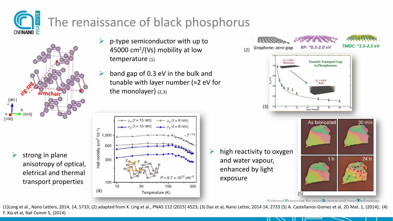
The renaissance of black phosphorus
(1)Long et al., Nano Letters, 2014, 14, 5733; (2) adapted from X. Ling et al., PNAS 112 (2015) 4523; (3) Das et al, Nano Letter, 2014 14, 2733 (5) A. Castellanos-Gomez et al, 2D Mat. 1, (2014); (4) F. Xia et al, Nat Comm 5, (2014)
p-type semiconductor with up to 45000 cm2/(Vs) mobility at low temperature (1)
band gap of 0.3 eV in the bulk and tunable with layer number (≈2 eV for the monolayer) (2,3)
strong in planeanisotropy of optical, eletrical and thermaltransport properties
high reactivity to oxygenand water vapour, enhanced by light exposure
(2)
(3)
(4)(5)

Ohmic contact engineering
Tunneling barrier<<<<
Schottky barrier
Metallization below the contact
metal electrode
The simplest model: Schottky-Mott rule
𝜙𝑝 = 𝐸𝑔 − 𝜙𝑚 − 𝜒
𝜒𝑏𝑃 ≈ 4.4 𝑒𝑉
𝜙𝑛 = 𝜙𝑚 − 𝜒
<<<<
<<<<
Ohmic contact Titanium
Chromium
Nickel
Often usedas stitchinglayer for goldelectrodes
(6)
(7) (8)
𝜙𝑁𝑖 ≈ 5.0 𝑒𝑉
𝜙𝐶𝑟 ≈ 4.5 𝑒𝑉
𝜙𝑇𝑖 ≈ 4.3 𝑒𝑉
best for hole injection
less suitable for hole injection
<<<<
(9)
(10)
(11)
(6) Wikipedia Cc licence; (7) adapted from Schroder, Semiconductor materials and device characterization; (8) Feng et al, Nanoscale, 2016, 8, 2686; (9)Allain et al, Nat Mater, 2015, 14, 1195; (10) Lide, Handbook of Chemistry and Physics, 2008; (11) Du et al, ACS Nano, 2014, 8, 10035

Transfer Length Method
𝑅2 = 𝑅𝐶 + 𝑅𝑏𝑃 𝑐ℎ𝑎𝑛𝑛𝑒𝑙 + 𝑅𝐶
𝑅𝑏𝑃𝑐ℎ𝑎𝑛𝑛𝑒𝑙 = (𝑑/𝑊)𝑅𝑆 ∝ 𝑑
d= n*d1
W
d1 d1
L
I
V=

Transfer Length Method
d1 2d1 3d1 4d1 5d1 6d1 7d1
R2
d
RS/W
2Rc
𝑅2 = 𝑅𝐶 + 𝑅𝑏𝑃 𝑐ℎ𝑎𝑛𝑛𝑒𝑙 + 𝑅𝐶
𝑅𝑏𝑃𝑐ℎ𝑎𝑛𝑛𝑒𝑙 = (𝑑/𝑊)𝑅𝑆 ∝ 𝑑
d= n*d1
W
d1 d1
L
I
V=

Transfer Length Method
Aggregate data over different devices/samples
Normalization of the resistance with contact width to compare different devices
Average
Propagation of the experimental error
Standard error of the distribution to get information on the scattering among the devices
𝑅𝐶𝑊d= n*d1
W
d1 d1
L
I
V=

Sample preparation
0.0 0.5 1.0 1.50
5
10
15
20
25
30
35
z (
nm
)
x (m)
Exfoliation in glove box or in glove bag
Coating with a MMA:MAA/PMMA bilayer
Flakes identification and EBL
Development&O2 plasma
Metal evaporation, lift-off, coating
10 µm

-1 0 1
-150
-75
0
75
150
I(nA)
V(mV)
d=5m R=23.2k
d=4m R=18.6k
d=3m R=14.1k
d=2m R=10.3k
d=1m R=6.2k
Room T
Cr
-1 0 1
-150
-75
0
75
150
I(nA)
V(mV)
d=5m
d=4m
d=3m
d=2m
d=1m
Room T
Cr
I-V Curves
All curves show linear behavior Good quality Ohmic contacts No Schottky behaviour
Linear fit to extract R2
d= n*d1
W
d1 d1
L
I
V=

Contact resistance at room temperature
0 1 2 3 4 50
5
10
15
20
25
R2
(k
)
d (m)
Room T
Cr
Ti
Ni
0.0 0.1 0.20.00
0.25
0.50
0.75
1.00
1.25
1.50
R2
(k
)
d (m)
Room T
Cr
Ti
Ni
𝑅𝐶|𝑁𝑖 < 𝑅𝐶|𝑇𝑖 < 𝑅𝐶|𝐶𝑟
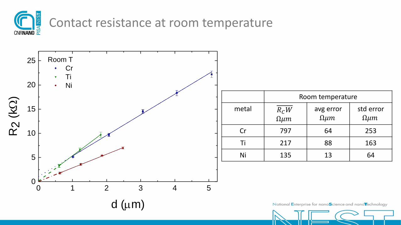
Contact resistance at room temperature
Room temperature
metal 𝑅𝐶𝑊Ω𝜇𝑚
avg errorΩ𝜇𝑚
std errorΩ𝜇𝑚
Cr 797 64 253
Ti 217 88 163
Ni 135 13 64
0 1 2 3 4 50
5
10
15
20
25
R2
(k
)
d (m)
Room T
Cr
Ti
Ni

Contact resistance at low temperature
0 1 2 3 4 50
10
20
30
40
50
60
R2
(k
)
d (m)
T= 4.2 K
Cr
Ti
Ni
0.0 0.1 0.20.0
0.5
1.0
1.5
2.0
2.5
3.0
3.5
4.0
R2
(k
)
d (m)
T= 4.2 K
Cr
Ti
Ni
Low temperature
metal 𝑅𝐶𝑊Ω𝜇𝑚
avg errorΩ𝜇𝑚
std errorΩ𝜇𝑚
Cr 2428 198 1377
Ti 740 209 282
Ni 432 30 208

10 100
0
2000
4000
Cr
Ti
Ni
RCW
(
m)
Temperature (K)
• Ni has the lowest contact resistance and the lowest scattering between devices, both at RT and at LT.
• RcW = 135 m for Ni at RT is among the lowest values reported.
• Cr shows the worst performance, likely due to a defective growth of Cr on bP.
Contact resistance: summary
(12) Adapted from Hong et al, J. Phys Chem C, 2015, 119, 8199; (13) Pan et al, Chem Mater, 2016, 28, 2100

High bias and gate voltage dependence
-0.10 -0.05 0.00 0.05 0.10-30
-20
-10
0
10
20
30
Cr
Ti
Ni
I sd (A
)
Vsd
(V)
Vg=0
-80 -40 0 40 800.3
0.4
0.5
0.6
0.7
0.8
0.9
1.0
Cr
Ti
Ni
Ad
juste
d-r
2
Vg (V)
In the accumulation regime, all contacts display an Ohmic behavior, even up to ±100 mV bias.
Reaching the depletion regime, deviations from the Ohmic behaviour are observed, independently of the metal, consistent with previous reports.(14)
(14) Li et al, Nat. Nanotech, 9, 372
-80 -40 0 40 80
0
10
20
30
40
Ni
Cr
Ti
I sd (
A)
Vg(V)
-80 -40 0 40 80
1E-4
1E-3
0.01
0.1
1
10
Ni
Cr
Ti
I sd (
A)
Vg(V)

Approaching the quantum limit
Conclusions
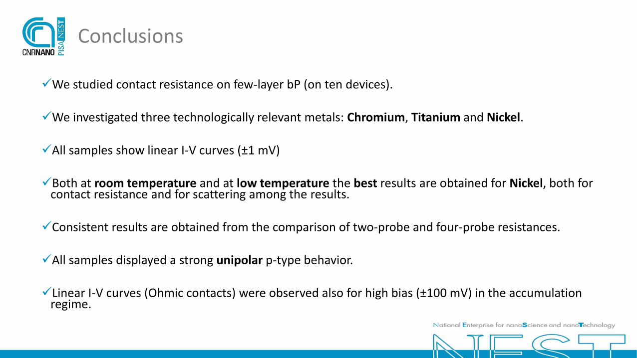
We studied contact resistance on few-layer bP (on ten devices).
We investigated three technologically relevant metals: Chromium, Titanium and Nickel.
All samples show linear I-V curves (±1 mV)
Both at room temperature and at low temperature the best results are obtained for Nickel, both for contact resistance and for scattering among the results.
Consistent results are obtained from the comparison of two-probe and four-probe resistances.
All samples displayed a strong unipolar p-type behavior.
Linear I-V curves (Ohmic contacts) were observed also for high bias (±100 mV) in the accumulation regime.

Acknowledgements
Thank you for your attention!
“Phosphorene functionalization: a new platform for advanced
multifunctional materials” (Grant Agreement No. 670173)
M. Serrano-Ruiz M. Peruzzini
S. ToffaninF. Prescimone
G. le GalF. Telesio