Embed Size (px)
Citation preview
On the Drift Behaviors of a Phase Change Memory (PCM) Cell
Pilin Junsangsri Student IEEE, Jie Han Member IEEE, and Fabrizio Lombardi Fellow IEEE
Abstract—This paper presents a HSPICE macromodel of a
phase change memory (PCM) by considering the phenomenon
of drift behavior as leading to incorrect operation. The model
simulates the behavior due to the drift in the resistance and
threshold voltage when the cell is not been read or
programmed. It considers not only the resistance change by
phase (as corresponding to the two phases, amorphous and
crystalline), but also the temperature, the crystalline fraction
and the continuous profile of the resistance. This electrical
based modeling by HSPICE allows to fully characterizing the
holding voltage and the continuous behavior of the PCM
resistance, while assessing the impact of the programming time
of the drifted parameters. The proposed macromodel generates
the I-V and R-I plots of a PCM cell at a very small error
compared with experimental data. A detailed sensitivity
analysis of the electrical parameters of the PCM cell is pursued
to show the robust characteristics of the proposed macromodel
to capture the variation in parameters due to drift.*
I. INTRODUCTION
With the fast growing market of consumer electronics
and the increased demand on large storage, new non-volatile
memories (NVMs) are attracting attention to meet the
technological challenges of CMOS. Phase change memories
(PCM) [1] have been advocated for replacing flash
memories, because a PCM cell is not only significantly
faster and smaller, but it is also very reliable (up to 100
million write cycles) [2]. The integration of a PCM into an
IC requires tool compatibility for simulation, such as
HSPICE. HSPICE allows establishing the electrical
characteristics of the operation of a PCM cell and
facilitating its interface with peripheral circuits and other
functional blocks for chip design [1]. A comprehensive
assessment of a PCM cell however, remains elusive; many
simulation models based on HSPICE can be found in the
technical literature. These models are accurate, but they
focus on specific parameters, thus often not fully addressing
important operational features. Among these features, the
drift behavior of a PCM cell is very important for its
commercialization. Drift negatively affects two parameters,
the resistance and the threshold voltage. Changes in these
parameters cause malfunctioning of the memory, thus
affecting its correctness and storage capabilities. The drift
behavior of a PCM cell is dependent on programming time
* P. Junsangsri is with the Electrical and Computer Engineering
Department, Northeastern University, Boston, MA 02115, USA (e-mail:
J. Han is with the Electrical and Computer Engineering Department, University of Alberta, Edmonton, Canada (e-mail: [email protected])
F. Lombardi is with the Electrical and Computer Engineering
Department, Northeastern University, Boston, MA 02115, USA (e-mail: [email protected])
and the resistance range. Resistance drift is not significant
for a binary PCM cell because its range increases over time;
however for multilevel storage, the drift adversely affects
cell operation because the distance between adjacent levels
is small and over time, stochastic fluctuations of the
resistance are likely to cause an overlap [3].
In this paper, the HSPICE-based macromodel of a PCM
cell of [4] is extended to the drift behaviors. The proposed
PCM macromodel is versatile, comprehensive and is used to
assess drifts in threshold voltage and resistance by utilizing
temperature profiling effects and the crystalline fraction of a
PCM cell. This electrical based model by HSPICE allows to
fully characterizing the holding voltage and the continuous
behavior of the PCM resistance. So differently from
previous models (such as [1]), the proposed macromodel
also incorporates resistance and threshold voltage drifts to
comprehensively simulate and assess a PCM. Simulation
results are presented; they show that the proposed
macromodel is very accurate and robust (following an
extensive analysis of parameter sensitivity).
II. REVIEW
In a Phase Change Memory (PCM), data storage relies
on the reversible phase transformation of the chalcogenide
alloy (e.g. Ge2Sb2Te5, GST) between the amorphous and the
crystalline phases. The amorphous phase has a high
resistance and is commonly referred to as the reset state; the
crystalline phase has a low resistance and is referred to as
the set state [5]. The PCM device is fabricated by using a
thin film chalcogenide layer in contact with a metallic
heater. A pulse with a high amplitude is used to melt and
quench the PC element to an amorphous phase (Reset State),
while a longer pulse with a low amplitude is used to
crystallize the PC element to a crystalline phase (Set State)
[1]. Since switching between the amorphous and crystalline
phases is based on the crystalline fraction of the PCM, the
electrical resistance of the PCM cell is given as
( ) (1)
Where Rc and Ra are the resistances of the PCM when it
is fully crystalline and amorphous respectively. Cx is the
crystalline fraction: when Cx is equal to zero, the PCM is
fully amorphous; when Cx is equal to one, the PCM is fully
crystalline [5].
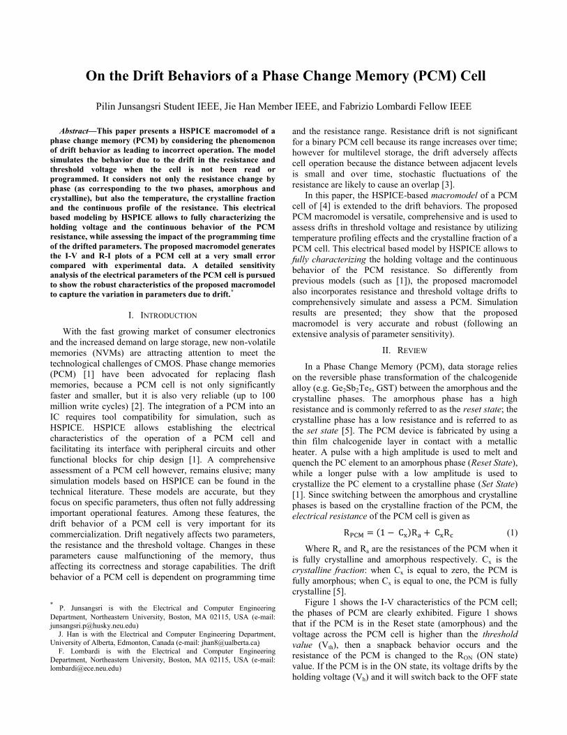
Figure 1 shows the I-V characteristics of the PCM cell;
the phases of PCM are clearly exhibited. Figure 1 shows
that if the PCM is in the Reset state (amorphous) and the
voltage across the PCM cell is higher than the threshold
value (Vth), then a snapback behavior occurs and the
resistance of the PCM is changed to the RON (ON state)
value. If the PCM is in the ON state, its voltage drifts by the
holding voltage (Vh) and it will switch back to the OFF state
(set or reset state) if and only if the voltage across the PCM
is less than the ON/OFF Intersection Point (VX). In Figure
1, the threshold voltage of PCM cell is approximately
0.75V, while the holding voltage (Vh) and the ON/OFF
intersection point of the PCM cell (VX) are approximately
0.45V and 0.53V respectively.
Figure 1. I-V Characteristic of PCM cell when it’s in Set, Reset, Partial
Set, and Partial Reset State [6].
To simulate the electrical characteristics of a PCM,
different models have been proposed in the technical
literature. [5] has presented a compact SPICE model with
Verilog-A; the resistance of the PCM is based on(1);
however, [5] is unable to simulate the I-V curve of a PCM,
because it does not consider the holding voltage and the
crystallized rate. [1] has presented a detailed HSPICE
model; however, the change in resistance of a PCM is not
continuous and the holding voltage is not considered, thus
failing to generate the I-V curve. In addition to the above
three, other models can be found in the technical literature
[6, 7, 8, 9]; however, these models encounter the same
limitations and disadvantages, such as ignoring the holding
voltage, discontinued behavior of the PCM resistance,
lacking of verification with simulation data, or utilization of
model parameters that are not compatible with an HSPICE
simulation environment.
III. MACROMODELING
This section presents the basic principles of the proposed
model; this is a macrolevel model (hereafter referred to as
macromodel) and its flow chart is shown in Figure 2 of [4].
The macromodel consists of two models: the basic model
and the advanced model. For the basic model (shown in the
flowchart in Figure 2), the input and output voltages are
provided to the PCM circuit (Figure 3a) to establish its state
(ON or OFF) and calculate the resistance. Figure 3a shows
the circuit model of the PCM cell; nodes in and out are the
input and output nodes in Figure 2. When there is a voltage
difference across in and out, the Control ON State blocks
(Figure 2) checks the state of the PCM, i.e. ON or OFF. If it
is the ON state, the switch sw2 is ON, while switch sw1 is
OFF. The resistance of the PCM is reduced to the RON
value. The voltage source Vh is added to simulate the
holding voltage in the I-V characteristics of the PCM. When
the PCM is in the OFF state, the switch sw1 is ON, while
the switch sw2 is OFF. The resistance of the PCM cell is
based on the crystalline fraction of the PCM as calculated
using (1).
Figure 2. Flowchart of the proposed PCM macromodel.
Figure 3. Basic model of Phase Change Memory (PCM) cell a) Main
circuit b) Temperature Comparator (Decision Circuit) c) Crystalline
fraction calculation circuit d) Control Switch Circuit e) Integrator Circuit
After establishing the state and the resistance of the
PCM cell, the temperature is found as in [5] and a decision
circuit (Figure 3b) is used to find the behavior of the PCM.
Let Tr correspond to the temperature estimate of the PCM;
to check whether the PCM is in the programming state, the
temperature must be compared with the glass transition
point (Tx) and the melting point (Tm). If the temperature of
the PCM cell is less than Tx, the resistance remains the
same. If the temperature is higher than Tx but lower than Tm,
then the PCM is programmed to the crystalline phase.
However if the temperature of the PCM is higher than Tm,
then the PCM is programmed to the amorphous phase.
Based on the decision circuit (Figure 3b), the voltage at
node TxTr represents the voltage difference between Tx and
Tr, while the voltage at node TmTr represents the voltage
difference between Tm and Tr. In the decision circuit (Figure
3b), when the voltage at node TxTr is positive, the switch
sw_dc1 is OFF, while switch sw_dc3 is ON. When the
voltage at node TmTr is positive, switches sw_dc2 and
sw_dc6 are ON while switches sw_dc4 and sw_dc5 are
OFF. So, the programming behavior of the PCM cell is fully
controlled. The crystalline fraction calculation circuit
(Figure 3c) is employed for varying the crystalline fraction
(Cx) of the PCM cell. Switches sw_cx2 and sw_cx3 depend
on the output voltage of the decision circuit that controls the
programming behavior of the PCM cell; the switches
sw_cx1 and sw_cx4 are ON when the PCM is in the ON
state. The ON/OFF state of the circuit must be considered
next; a Schmitt Trigger (Figure 3d) is employed to control
the ON/OFF state of the circuit. The state of the circuit
(ON/OFF) is controlled by comparing the voltage difference
across the bitline with the threshold and the ON/OFF
intersection point voltages.
However, based on the I-V characteristics of the PCM
(Figure 1), the programming behavior of the cell is related
to the threshold voltage and the crystalline fraction. If the
PCM cell is in the amorphous or intermediate phase, voltage
across it must be higher than its threshold value (Vth,new) for
programming to take place. If the PCM is in the crystalline
phase, the voltage across it must be higher than Vx for
programming to take place.
The relationship between the threshold voltage and the
crystalline fraction (Cx) can be expressed as follows.
( ) (2)
where Vth,new is the threshold voltage of the PCM cell when
its crystalline fraction is varied (i.e. not constant), Vth is the
threshold voltage of the PCM cell when the crystalline
fraction is equal to zero, Cx is the crystalline fraction of the
PCM cell and is calculated from the voltage at node Cx of
Figure 3c. Vx is the intersection point of the ON and OFF
states (as shown in Figure 1); its value is given by
(3)
Where Vh is the holding voltage, Rset is the resistance of the
PCM cell when it is in the full crystalline phase, and RON is
the resistance of the PCM cell when it is in the ON-state.
Next, a discussion of a recently proposed PCM
macromodel [1] is pursued. Consider the circuit of the
model of [1]; the PCM resistance is switched to Rm when
the PCM is in fully amorphous phase and the temperature is
higher than the melting point (Tm). So, the rate of change of
the resistance of the PCM is not considered in [1] because
the time of the write operation from the amorphous to the
crystalline phases (or vice versa) is erroneously based on the
delay encountered by the macromodel circuit, not its
simulated value. The logic control circuit of [1] finds that
the PCM resistance is always given by Rx when the
temperature of the PCM is less than Tm and Rm when the
temperature of the PCM is higher than the melting point and
Cx is less than 100%. However if the temperature of the
PCM is higher than the melting point and the crystalline
fraction is 100%, then the PCM resistance is based on the
previous state of PCM cell. So, when the voltage difference
across the PCM is very small (such as during a read
operation), the PCM resistance is always given by Rx as
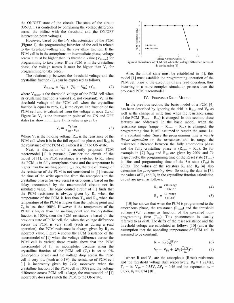
incorrect value. Figure 4 shows the PCM resistance of the
macromodel of [1] when the voltage difference across the
PCM cell is varied; these results show that the PCM
macromodel of [1] is incomplete, because when the
crystalline fraction of the PCM cell (Cx) is set to 0%
(amorphous phase) and the voltage drop across the PCM
cell is very low (such as 0.1V), the resistance of PCM cell
[1] is incorrectly given by 7kΩ; moreover, when the
crystalline fraction of the PCM cell is 100% and the voltage
difference across PCM cell is large, the macromodel of [1]
incorrectly does not switch the PCM to the ON-state.
Figure 4. Resistance of PCM cell when the voltage difference across it
is varied using [1]
Also, the initial state must be established in [1]; this
model [1] must establish the programming operation of the
PCM cell prior to the execution of any read operation, thus
incurring in a more complex simulation process than the
proposed PCM macromodel.
IV. PROPOSED DRIFT MODEL
In the previous section, the basic model of a PCM [4]
has been described by ignoring the drift in Rreset and Vth as
well as the change in write time when the resistance range
of the PCM (Rreset – Rset) is changed. In this section, these
features are addressed. In the basic model, when the
resistance range (range = Rreset – Rset) is changed, the
programming time is still assumed to remain the same, i.e.
at a constant value. Since the programming time is nearly
linear dependent on the resistances and its range, the
resistance difference between the fully amorphous phase
and the fully crystalline phase is (Rreset – Rset). So for
example in [7] Rreset and Rset are given by 200k and 7k
respectively; the programming time of the Reset state (Treset)
is 10ns and programming time of the Set state (Tset) is
200ns. The values of the resistors Rc and Rd [4] also
determine the programming time. So using the data in [7],
the values of Rc and Rd in the crystalline fraction calculation
circuit are given as follows.
(4)
(5)
[10] has shown that when the PCM is programmed to the
amorphous phase, the resistance (Rreset) and the threshold
voltage (Vth) change as function of the so-called non-
programming time (Toff). This phenomenon is usually
referred to as drift. The drifts of the reset resistance and the
threshold voltage are calculated as follows [10] (under the
assumption that the annealing temperature of PCM cell is
assumed to be constant).
(
) (6)
(
) (7)
where R and VT are the amorphous (Reset) resistance
and the threshold voltage drift respectively, R0 = 1.28MΩ,
T0 = 1s, VT0 = 0.55V, = 0.46 and the exponents =
0.077, = 0.074 [10].
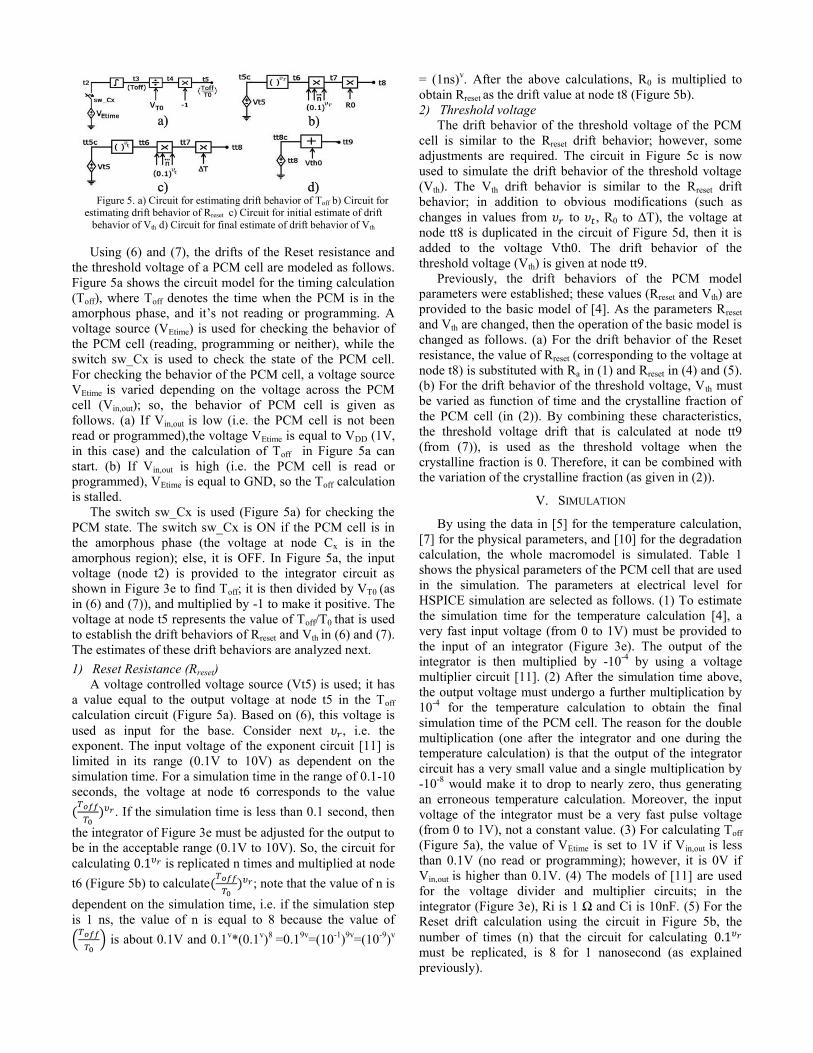
Figure 5. a) Circuit for estimating drift behavior of Toff b) Circuit for
estimating drift behavior of Rreset c) Circuit for initial estimate of drift
behavior of Vth d) Circuit for final estimate of drift behavior of Vth
Using (6) and (7), the drifts of the Reset resistance and
the threshold voltage of a PCM cell are modeled as follows.
Figure 5a shows the circuit model for the timing calculation
(Toff), where Toff denotes the time when the PCM is in the
amorphous phase, and it’s not reading or programming. A
voltage source (VEtime) is used for checking the behavior of
the PCM cell (reading, programming or neither), while the
switch sw_Cx is used to check the state of the PCM cell.
For checking the behavior of the PCM cell, a voltage source
VEtime is varied depending on the voltage across the PCM
cell (Vin,out); so, the behavior of PCM cell is given as
follows. (a) If Vin,out is low (i.e. the PCM cell is not been
read or programmed),the voltage VEtime is equal to VDD (1V,
in this case) and the calculation of Toff in Figure 5a can
start. (b) If Vin,out is high (i.e. the PCM cell is read or
programmed), VEtime is equal to GND, so the Toff calculation
is stalled.
The switch sw_Cx is used (Figure 5a) for checking the
PCM state. The switch sw_Cx is ON if the PCM cell is in
the amorphous phase (the voltage at node Cx is in the
amorphous region); else, it is OFF. In Figure 5a, the input
voltage (node t2) is provided to the integrator circuit as
shown in Figure 3e to find Toff; it is then divided by VT0 (as
in (6) and (7)), and multiplied by -1 to make it positive. The
voltage at node t5 represents the value of Toff/T0 that is used
to establish the drift behaviors of Rreset and Vth in (6) and (7).
The estimates of these drift behaviors are analyzed next.
1) Reset Resistance (Rreset)
A voltage controlled voltage source (Vt5) is used; it has
a value equal to the output voltage at node t5 in the Toff
calculation circuit (Figure 5a). Based on (6), this voltage is
used as input for the base. Consider next , i.e. the
exponent. The input voltage of the exponent circuit [11] is
limited in its range (0.1V to 10V) as dependent on the
simulation time. For a simulation time in the range of 0.1-10
seconds, the voltage at node t6 corresponds to the value
(
) . If the simulation time is less than 0.1 second, then
the integrator of Figure 3e must be adjusted for the output to
be in the acceptable range (0.1V to 10V). So, the circuit for
calculating is replicated n times and multiplied at node
t6 (Figure 5b) to calculate(
) ; note that the value of n is
dependent on the simulation time, i.e. if the simulation step
is 1 ns, the value of n is equal to 8 because the value of
(
) is about 0.1V and 0.1
v*(0.1
v)
8 =0.1
9v=(10
-1)
9v=(10
-9)
v
= (1ns)v. After the above calculations, R0 is multiplied to
obtain Rreset as the drift value at node t8 (Figure 5b).
2) Threshold voltage
The drift behavior of the threshold voltage of the PCM
cell is similar to the Rreset drift behavior; however, some
adjustments are required. The circuit in Figure 5c is now
used to simulate the drift behavior of the threshold voltage
(Vth). The Vth drift behavior is similar to the Rreset drift
behavior; in addition to obvious modifications (such as
changes in values from to , R0 to ΔT), the voltage at
node tt8 is duplicated in the circuit of Figure 5d, then it is
added to the voltage Vth0. The drift behavior of the
threshold voltage (Vth) is given at node tt9.
Previously, the drift behaviors of the PCM model
parameters were established; these values (Rreset and Vth) are
provided to the basic model of [4]. As the parameters Rreset
and Vth are changed, then the operation of the basic model is
changed as follows. (a) For the drift behavior of the Reset
resistance, the value of Rreset (corresponding to the voltage at
node t8) is substituted with Ra in (1) and Rreset in (4) and (5).
(b) For the drift behavior of the threshold voltage, Vth must
be varied as function of time and the crystalline fraction of
the PCM cell (in (2)). By combining these characteristics,
the threshold voltage drift that is calculated at node tt9
(from (7)), is used as the threshold voltage when the
crystalline fraction is 0. Therefore, it can be combined with
the variation of the crystalline fraction (as given in (2)).
V. SIMULATION
By using the data in [5] for the temperature calculation,
[7] for the physical parameters, and [10] for the degradation
calculation, the whole macromodel is simulated. Table 1
shows the physical parameters of the PCM cell that are used
in the simulation. The parameters at electrical level for
HSPICE simulation are selected as follows. (1) To estimate
the simulation time for the temperature calculation [4], a
very fast input voltage (from 0 to 1V) must be provided to
the input of an integrator (Figure 3e). The output of the
integrator is then multiplied by -10-4
by using a voltage
multiplier circuit [11]. (2) After the simulation time above,
the output voltage must undergo a further multiplication by
10-4
for the temperature calculation to obtain the final
simulation time of the PCM cell. The reason for the double
multiplication (one after the integrator and one during the
temperature calculation) is that the output of the integrator
circuit has a very small value and a single multiplication by
-10-8
would make it to drop to nearly zero, thus generating
an erroneous temperature calculation. Moreover, the input
voltage of the integrator must be a very fast pulse voltage
(from 0 to 1V), not a constant value. (3) For calculating Toff
(Figure 5a), the value of VEtime is set to 1V if Vin,out is less
than 0.1V (no read or programming); however, it is 0V if
Vin,out is higher than 0.1V. (4) The models of [11] are used
for the voltage divider and multiplier circuits; in the
integrator (Figure 3e), Ri is 1 Ω and Ci is 10nF. (5) For the
Reset drift calculation using the circuit in Figure 5b, the
number of times (n) that the circuit for calculating must be replicated, is 8 for 1 nanosecond (as explained
previously).

TABLE I. PHYSICAL PARAMETERS FOR PCM SIMULATION
Parameters Value
Radius of active region (r1) 50 nm
Radius of PCM cell (r2) 100 nm
Thermal conductivity of Ge2Sb2Te5 (k) 4.63*10-3 J.cm.K-1.S-1
Thermal capacity of Ge2Sb2Te5 (C) 1.25 J.cm-3K-1
Volume of PCM cell (V) 7*10-14 cm3
Glass Transition Point (Tx) 200 C
Melting Point (Tm) 600 C
Static resistance of reset (Rreset) 200 kΩ
Static resistance of set (Rset) 7 kΩ
Dynamic-On Resistance (Ron) 1 kΩ
Threshold Voltage (Vth) 0.78 V
Holding Voltage (Vh) 0.45 V
Programming time of Reset (Treset) 10 ns
Programming time of Set (Tset) 200 ns
To assess the electrical characteristics of a PCM cell, the
so-called R-I curve must be generated; this plot allows to
test the validity of the proposed macromodel with data
obtained from fabricated devices. A pulse sequence must be
provided for generating the R-I curve; this sequence consists
of Reset, Read and Set pulses with increasing amplitude for
the Set pulse until it reaches the same amplitude as the Reset
pulse [2]. The simulated R-I curve of the PCM is given in
Figure 6a.
Figure 6. a) I-R curve of PCM cell b)I-V curve of PCM cell
Figure 6b shows the simulation-generated I-V curve of
the PCM cell when its initial state is full amorphous (Cx =
0), full crystalline (Cx = 1), or partial (Cx = 0.9). The
simulation results show that the snapback behavior of the
PCM cell is generated by the proposed macromodel and the
threshold voltage is dependent on the crystalline fraction;
this plot closely resembles Figure 1 [6]. A comparison
between the proposed macromodel and the experimental
characterization of [10] (i.e. (6) and (7)) is pursued next.
Figure 7 shows both of these plots; the proposed PCM
macromodel generates the I-V plot that closely resembles
the experiment data of [10] by considering all the electrical
features of a PCM. By considering a constant number of
circuits for the calculation of (i.e. 8) in the
macromodel, the degradation in the values of Rreset and Vth
due to drift are also found.
Figure 7. I-V plots of PCM cell from experimental data [10] and
proposed PCM macromodel
Figure 8. Percentage error in drift of Rreset and Vth between macromodel
and experimental data of [10]
The plots for the error are shown in Figure 8; when Toff
is less than 100ns, the errors (in percentage) for Rreset and Vth
are very low and nearly constant. However, when Toff
increases, the error percentage increases over time because
the accuracy of the exponentiation circuit in the proposed
macromodel is limited to an input voltage from 0.1 to 10V.
Next, the sensitivity of the proposed macromodel to
different parameters is assessed with respect to the I-V
characteristics. In all cases only a single parameter is
changed at a 5%, level (i.e. all other parameters are left
unchanged to their default values).
TABLE II. SUMMARY OF PARAMETERS SENSITIVITY
Variation Parameter Sensitive Parameter
Rreset Rreset, Treset, RPCM
Rset Rset, Tset, RPCM,Vth, Vx
RON RON, Vth, Vx
Vth Vth
Vh Vth, Vx, Vh
Table 2 shows the summary of the sensitivity of each
parameter. Table 2 shows that only the variations in the
threshold voltage (Vth) is not affected by other parameters.
However for the other parameters, any variation causes
changes especially, in Rset, RON, and Vh (i.e. for Vx in (3))
and also in Vth (as in (2)). Based on (1), the variations of
Rreset and Rset result in a change of RPCM when the crystalline
fraction of PCM is not zero (Cx ≠ 0). Also the write time
(Treset and Tset) changes upon variation of Rreset and Rset. So
while a variation of Vth has no effect (i.e. it only affects
itself), Rset is the parameter that is sensitive to most
parameters.
Reset Resistance (RReset): The results of varying the reset
resistance (Rreset) are given in Tables 3 and 4. As described
previously, a change in the value of the reset resistance
(Rreset) affects the write time (as shown in Table 3) in nearly
a linear fashion. Moreover based on (1), the PCM resistance
(RPCM) is dependent on the crystalline fraction (Cx), Rset and
Rreset. When reset resistance is changed, the new values of
RPCM (at the same crystalline fraction) are given in Table 4.
TABLE III. WRITE TIME (TRESET) WHEN RRESET IS VARIED
%
Variation
Reset
Resistance (kΩ)
PCM Resistance
Range (kΩ)
Write Time,
Treset (ns)
0 200 193 10
-5 190 183 9.482
+5 210 203 10.518
TABLE IV. RPCM AT THE SAME CRYSTALLINE FRACTION
% Variation Rreset (kΩ) RPCM (kΩ)
Cx = 0 Cx = 0.5 Cx = 1
0 200 200 103.5 7
-5 190 190 98.5 7
+5 210 210 108.5 7
Set Resistance (Rset): Based on (3), the ON/OFF
intersection point of PCM (Vx) is dependent on Rset; the plot
of Vx versus Rset is shown in Figure 9.
Figure 9. ON/OFF state intersection point (Vx) Vs Set resistance (Rset)
When Rset is higher than 2kΩ, Vx reaches a steady value
because (Rset – RON) is higher than 1kΩ (as in (3)), and
therefore Vx is less than VhRset. This confirms the sensitivity
of Vx at low values of Rset thus showing the criticality of the
Set resistance in the operation of a PCM cell.
Threshold Voltage (Vth): The threshold voltage (Vth) under
a variation of Rset depends on Vx and Cx (as per (2)). If the
PCM cell is in a fully amorphous phase (Cx = 0) the
threshold voltage is 0.78V. Table 5 shows the threshold
voltage when the crystalline fraction (Cx) is varied. At a
fixed crystalline fraction (and Cx≠ 0), Table 5 shows that the
threshold voltage has a minor inverse sensitivity to Rset.
TABLE V. THRESHOLD VOLTAGE OF THE PCM WHEN RSET IS VARIED
% Variation Rset (kΩ) Vth (Volt)
Cx=0 Cx = 0.1 Cx = 0.5 Cx= 1
Normal 7 0.78 0.7545 0.6525 0.5250
-5% 6.65 0.78 0.7550 0.6548 0.5296
5% 7.35 0.78 0.7541 0.6504 0.5209
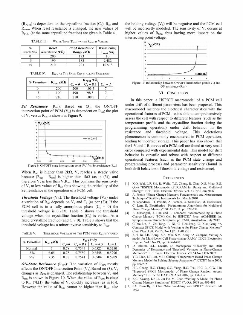
ON-State Resistance (RON): The variation of RON mostly
affects the ON/OFF Intersection Point (Vx).Based on (3), Vx
changes as RON is changed. The relationship between Vx and
RON is shown in Figure 10. When the value of RON is close
to Rset (7kΩ), the value of Vx quickly increases (as in (6)).
However the value of RON cannot be higher than Rset, else
the holding voltage (Vh) will be negative and the PCM cell
will be incorrectly modeled. The sensitivity of Vx occurs at
higher values of RON, thus having more impact on the
intersecting point voltage.
Figure 10. Relationship between ON/OFF intersection point (Vx) and
ON resistance (RON)
VI. CONCLUSION
In this paper, a HSPICE macromodel of a PCM cell
under drift of different parameters has been proposed. This
macromodel matches the electrical characteristics with the
operational features of PCM; so it's able to comprehensively
assess the cell with respect to different features (such as the
temperature profile and the crystalline fraction during the
programming operation) under drift behavior in the
resistance and threshold voltage. This deleterious
phenomenon is commonly encountered in PCM operation,
leading to incorrect storage. This paper has also shown that
the I-V and I-R curves of a PCM cell are found at very small
error compared with experimental data. This model for drift
behavior is versatile and robust with respect to different
operational features (such as the PCM state change and
programming process) and parameter sensitivity (found in
both drift behaviors of threshold voltage and resistance).
REFERENCES
[1] X.Q. Wei, L.P. Shi, R. Walia, T.C. Chong, R. Zhao, X.S. Miao, B.S. Quek “HSPICE Macromodel of PCRAM for Binary and Multilevel
Storage” IEEE Trans. Electron Devices. Vol. 53, No.1 Jan 2006
[2] A. Pronin “Phase Change Memory: Fundamentals and Measurement Techniques” Keithley Instruments Inc. March 2010
[3] N.Papahdreou, H. Pozidis, A. Pantazi, A. Sebastian, M. Breitwisch,
C. Lam, E. Elecftheriou “Programming Algorithms for Multilevel Phase Change Memory” ISCAS 2011, pp. 329-332
[4] P. Junsangsri, J. Han and F. Lombardi “Macromodeling a Phase Charge Memory (PCM) Cell by HSPICE,” Proc. ACM/IEEE Int.
Symposium on Nanoarchitectures, pp. 77-84, Amsterdam, July 2012.
[5] C.Dao-Lin, S. Zhi-Tang, L. Xi, C. Hou-Peng, C. Xiao-Gang “A Compact SPICE Model with Verilog-A for Phase Change Memory”
Chin. Phys. Lett. Vol.28, No.1 (2011) 018501
[6] K.H. Jo, J.H. Bong, K.S. Min, S.M. Kang “A Compact Verilog-A model for Multi-Level-Cell Phase-change RAMs” IEICE Electronics
Express, Vol.6 No.19, pp. 1414-1420
[7] D. Ielmini, A.L. Lacaita, D. Mantegazza “Recovery and Drift Dynamics of Resistance and Threshold Voltages in Phase-Change
Memories” IEEE Trans. Electron Devices. Vol.54 No.2 Feb 2007
[8] Y.B. Liao, J.T. Lin, M.H. Chiang “Temperature-Based Phase Change Memory Model for Pulsing Scheme Assessment” ICICDT June 2008,
pp.199-202
[9] H.L. Chang, H.C. Chang, S.C. Yang, H.C. Tsai, H.C. Li, C.W. Liu “Improved SPICE Macromodel of Phase Change Random Access
Memory” IEEE VLSI DATE09, April 2009, pp. 134-137
[10] K.C. Kwong, Lin Li, Jin He, M. Chan “Verilog-A Model for Phase Change Memory Simulation” ICSICT 9th, Oct. 2008 pp. 492-495
[11] J.A. Connelly, P. Choi “Macromodeling with SPICE” Prentice Hall
1992