Embed Size (px)
Citation preview
On the modeling and simulation of of reaction-transferdynamics in semiconductor-electrolyte solar cells
Yuan He∗ Irene M. Gamba† Heung-Chan Lee‡ Kui Ren§
April 16, 2013
Abstract
The mathematical modeling and numerical simulation of semiconductor-electrolytesystems play important roles in the design of high-performance semiconductor-liquidjunction solar cells. We propose in this work a macroscopic mathematical model, a sys-tem of nonlinear partial differential equations, for the complete description of chargestransfer dynamics in such systems. The model consists of a reaction-drift-diffusion-Poisson system that models the transport of electron-hole pairs in the semiconductorregion and an equivalent system that describes the transport of reductant-oxidantpairs in the electrolyte region. The coupling between the semiconductor and the elec-trolyte is modeled through a set of interfacial reactive and current balance conditions.We present some numerical simulations to illustrate the quantitative behavior of thesemiconductor-electrolyte system in both dark and illuminated environments. We shownumerically that one can replace the electrolyte region in the system with a Schottkycontact only when the bulk reductant-oxidant pair density is extremely high. Other-wise, such replacement gives significantly inaccurate description of the real dynamicsof the semiconductor-electrolyte system.
Key words. Semiconductor-electrolyte system, reaction-drift-diffusion-Poisson system, semicon-ductor modeling, interfacial charge transfer, interface conditions, semiconductor-liquid junction,solar cell simulation, naso-scale device modeling.
1 Introduction
The mathematical modeling and simulation of semiconductor devices have been extensivelystudied in the past decades due to its importance in industrial applications; see [2, 29, 33,36, 39, 45, 46, 44, 63, 78, 80] for overviews of the field and [8, 34, 77, 90] for more details on
∗ICES,University of Texas, Austin, TX 78712; Email: [email protected] .†Department of Mathematics and ICES, University of Texas, Austin, TX 78712; Email:
[email protected] .‡Department of Chemistry, University of Texas, Austin, TX 78712; Email: [email protected] .§Department of Mathematics, University of Texas, Austin, TX 78712; Email: [email protected] .
1

the physics, classical and quantum, of semiconductor devices. In the recent years, the fieldis boosted significantly by the increasing need of simulation tools for designing efficient solarcells to harvest sunlight for clean energy. Various theoretical and computational results ontraditional semiconductor device modeling are revisited and modified to account for newphysics in solar cell applications. We refer interested reader to [27] for a summary of varioustypes of solar cells that have been constructed, [41, 55, 65] for simplified analytical solvablemodels that have been developed, and [18, 74, 51, 19, 32] for more advanced mathematicaland computational analysis on various models. Mathematical modeling and simulationprovide ways not only to improve our understanding on the behavior of the solar cells underexperimental conditions, but also to predict the performance of solar cells with generaldevice parameters and thus enable us to optimize the performance of the cells by selectingthe optimal combination of these parameters.
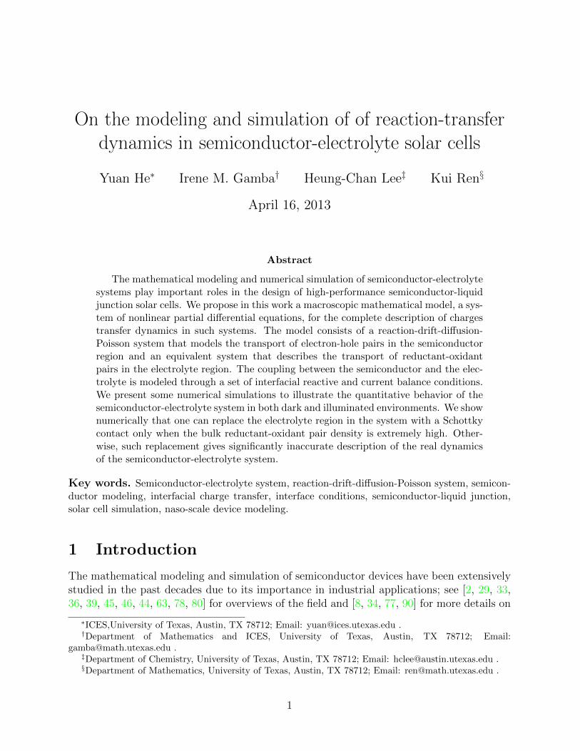
One popular type of solar cells, besides those made of semiconductor p-n junctions, arecells made of semiconductor-liquid junctions. A typical liquid-junction photovotaic solar cellconsists of four major components: the semiconductor, the liquid, the semiconductor-liquidinterface and the counter electrode; see a rough sketch in Fig. 1. Different semiconductor-liquid combinations can be utilized, see for instance [27, Tab. 1]. The working mechanism ofthis type of cells is as follows. When sunlight is absorbed by the semiconductor, electron-holepairs are generated. These electrons and holes are then separated by an applied potentialgradient across the device. The separation of the electrons and holes leads to electricalcurrent in the cell and concentration of charges on the semiconductor-liquid interface whereelectrochemical reactions and charge transfer occur.
The physics of charges transport in semiconductor-liquid junctions has been studied inthe past by many investigators; see [50] for a recent review. The mechanisms of chargegeneration, recombination and transport in both the semiconductor and the liquid are nowwell-understood. However, the reaction and charge transfer process on the semiconductor-liquid interface is far less understood despite the extensive recent investigations from boththe physical [30, 31, 48, 49, 68, 93] and the numerical simulation [65, 84] perspectives. Theobjective of this work is to mathematically model this interfacial charge transfer process sothat we could derive a complete system of equations to describe the whole charge transportprocess in the semiconductor-liquid junction.
To be specific, we consider here semiconductor-liquid junction with the liquid beingelectrolyte that contains reductants r and oxidants o with charge numbers αr and αo re-spectively. We denote by Ω ⊂ Rd (d = 1, 2, 3) the domain of the interest which containsthe semiconductor part ΩS and the electrolyte part ΩE. We denote by Σ ≡ ∂ΩE ∩ ∂ΩS theinterface between the semiconductor and electrolyte, ΓS = ∂Ω ∩ ∂ΩS the part of semicon-ductor boundary that is not in contact with the electrolyte, and ΓE = ∂Ω ∩ ∂ΩE the partof electrolyte that is not in contact with the semiconductor. We denote by Σ+ and Σ− thesemiconductor and the electrolyte sides of Σ respectively, and by ν(x) the unit outer normalvector at x ∈ ∂ΩS. Thus on the interface Σ, ν(x) points toward the electrolyte.
The mathematical modeling of the semiconductor-electrolyte system consists of threecomponents: the model for the dynamics of electron and holes in the semiconductor ΩS,the model for the dynamics of the reductants and oxidants in the electrolyte ΩE, and thereaction-transfer dynamics on the interface Σ. Boundary conditions on the ΓS and ΓE are
2
Semiconductor Liquid
Sun light
Collector Counter electrode
Figure 1: Sketch of the main components in a typical semiconductor-liquid junction solarcell.
specified by specific applications. For applications in solar cells, we have to also considerthe generation of electron-hole pairs in the the semiconductor ΩS due to the illumination bysunlight.
The rest of the paper is structured as follows. In Section 2 we first introduce the math-ematical model for the transport of electron-hole pairs in the semiconductor. We thenpresent the mathematical model for the dynamics of redox pairs in the electrolyte in Sec-tion 3. In Section 4 we present the interface conditions for densities and electrical field onthe semiconductor-electrolyte interface. Numerical schemes for the solution of the system insimplified setting are presented in Section 5 and some numerical simulations are shown inSection 6 where we exhibit the benefits of modeling the complete semiconductor-electrolytesystem. Concluding remarks are offered in Section 7.
2 Transport of electrons and holes
The modeling of transport of electrons and holes in semiconductor devices has been well-studied in the past decades [2, 29, 33, 36, 39, 63, 78, 80]. Many different models have beenproposed, such as the Boltzmann-Poisson system [6, 11, 17, 20, 26, 37, 39, 61, 67, 75], theenergy transport system [15, 23, 28, 39, 89, 82] and the drift-diffusion-Poisson system [1, 4,12, 13, 22, 21, 38, 63, 62, 74, 76, 81, 85, 88]. For the purpose of computational efficiency, weemploy the reaction-drift-diffusion-Poisson model in this work. Let us denote by T = (0, T ]the time interval that we are interested in. The bipolar drift-diffusion-Poisson model can bewritten in the following form
∂tρn +∇ · Jn = Rnp(ρn, ρp) + γGnp(x), in (0, T ]× ΩS
∂tρp +∇ · Jp = Rnp(ρn, ρp) + γGnp(x), in (0, T ]× ΩS
−∇ · (εSr∇Φ) =q
ε0[C(x) + ρp − ρn], in (0, T ]× ΩS.
(1)
with the current densities of electrons and holes are given respectively by
Jn = −Dn∇ρn + µnρn∇Φ,Jp = −Dp∇ρp − µpρp∇Φ.
(2)
3
Here ρn(t,x) and ρp(t,x) are the densities of the electrons and holes at time t and locationx respectively and Φ(t,x) is the electrical potential. The notation ∂t denotes the derivativewith respect to t while ∇ denotes the usual spatial gradient operator. The constant ε0 isthe dielectric constant in vacuum and the function εSr (x) is the relative dielectric functionof the semiconductor material. The function C(x) is the doping profile of the device. Thecoefficients Dn (resp. Dp) and µn (resp. µp) are the diffusivity and the mobility of electrons(resp. holes). These parameters can be computed from the first principles of statisticalphysics. In some practical applications, however, they can be fitted from experimental dataas well; see for example the discussion in [77]. The parameter q is the unit electric chargeconstant. The diffusivity and the mobility coefficients are related through the Einsteinrelations Dn = UT µn and Dp = UT µp with UT the thermal voltage at temperature T givenby UT = kB T /q, kB being the Boltzmann constant.
2.1 Charge generation and recombination
The function Rnp(ρn, ρp) is the generation-recombination rate, in other words, the rate atwhich electron-hole pairs are generated subtracted by the rate at which electron-hole pairsare recombined. Since electrons and holes are generated and recombined in pairs, we havethe same rate function for the two species. We consider in this work two types of generation-recombination models. The first one is the Auger model [63]. It is given by
Rnp(ρn, ρp) = (Anρn + Apρp)(ρ2i − ρnρp), (3)
where An and Ap are the Auger coefficients for electrons and holes respectively. For givenmaterials, An and Ap can be measured by experiments. The parameter ρi is the intrinsiccarrier density that is often calculated from the following formula [42]
ρi =√NcNv(
T300
)1.5e−Eg/(2kBT ) (4)
where the band gap at temperature T , Eg = Eg0 − αT 2/(T + β) with Eg0 the band gap atT = 0K (Eg0 = 1.17q for silicon for instance), α = 4.73 10−4q, and β = 636. The parametersNc and Nv are effective density of states in the conduction and the valence bands respectivelyat T = 300K.
The second generation-recombination model we consider is the Shockley-Read-Hall (SRH)model [63]. It reads
Rnp(ρn, ρp) =ρ2i − ρnρp
τp(ρn + ρi) + τn(ρp + ρi), (5)
where the coefficients τn and τp are the life time parameters for electrons and holes respec-tively. The values of these parameters are provided in Tab. 1 in Section 6.
When the semiconductor device is illuminated under the sun light, the device absorbsphoton energy, and electrons and holes can then be generated. This generation of chargesis modeled by the source function Gnp(x) in the transport equation (1). Once again, dueto the fact that electrons and holes are always generated in pairs, the generating functionsare the same for electrons and holes. We take a model that assumes that photons travelacross the device in straight lines. That is, we assume that photons do not get scattered
4
by the semiconductor material during their travel inside the device. This is a reasonableassumption for small devices that have been utilized widely [40]. Precisely, the generationof charges is given as
Gnp(x) =
σ(x)G0(x0)e−
∫ s0 σ(x0+s′θ0)ds′ , if x = x0 + sθ0
0, otherwise(6)
where x0 is the incident location, θ0 is the incident direction, σ(x) is the absorption coeffi-cient (integrated over usable wavelengths), and G0(x0) is the surface photon flux at x0. Thecontrol parameter γ ∈ 0, 1 in (1) is used to turn on and off the illumination mechanism.The cases of γ = 0 and γ = 1 are called dark and illuminated respectively in solar cellresearch community.
2.2 Boundary conditions
There are mainly two types of boundary conditions for the simulation in the semiconductorpart, depending on material we put in contact with the semiconductor: Dirichlet boundaryconditions at Ohmic contact and Neuman boundary conditions at Schottky contact. We de-note from now on ΓSo and ΓSs the Ohmic and Schottky parts of the semiconductor boundaryrespectively. We have ΓS = ΓSo ∪ ΓSs.
Dirichlet at Ohmic contacts. Ohmic contacts are used to model metal-semiconductorjunctions that do not rectify current. This type of contacts are mainly used to carry electricalcurrent out and into semiconductor devices, and should be fabricated with little (or ideallyno) parasitic resistance. Low resistivity Ohmic contacts are also essential for high-frequencyoperation. Mathematically, Ohmic contacts are modeled by Dirichlet boundary conditionswhich can be written as
ρn(t,x) = ρen(x), ρp(t,x) = ρep(x), on (0, T ]× ΓSo,Φ(t,x) = ϕbi + ϕapp, on (0, T ]× ΓSo,
(7)
where ϕbi and ϕapp are the built-in and applied potential, respectively. The boundary valuesρen, ρep for the Ohmic contacts are calculated following the assumptions that the semiconduc-tor is in stationary and equilibrium state and the charge neutrality condition holds. Thismeans that right-hand-side of the Poisson equation disappears so that
C + ρep − ρen = 0. (8)
Thermal equilibrium implies that the generation-recombination balance out so R = 0 atOhmic contacts. This leads to the mass-action law, between the density of electrons andholes:
ρenρep − ρ2
i = 0. (9)
The system of equations (8) and (9) admit a unique solution pair (ρn, ρp) which is given by
ρen(t,x) =1
2(√C2 + 4ρ2
i + C),
ρep(t,x) =1
2(√C2 + 4ρ2
i − C).(10)
5

These densities result in a built-in potential that can be calculated as
ϕbi = UT ln(ρen/ρi). (11)
Note that due to the fact that the doping profile C varies in space, these boundary valuesare different on different part of the boundary.
Robin (or Mixed) at Schottky contacts. More realistic metal-semiconductor junctionshave rectifying effects in the sense that current flow through the contacts are rectified.Schottky contacts are more realistic models of this type of metal-semiconductor junctions.Mathematically, at Schottky contact, Robin (also called mixed) type of boundary conditionsare imposed for the n- and p-components while Dirichlet type of conditions are imposed forthe Φ-component. More precisely, these boundary conditions are:
ν · Jn(t,x) = vn(ρn − ρen)(x), ν · Jp(t,x) = vp(ρp − ρep)(x), on (0, T ]× ΓSs,Φ(t,x) = ϕSchottky + ϕapp, on (0, T ]× ΓSs.
(12)
Here the parameters for the Schottky barrier are the recombination velocities vn and vp,and the height of the potential barrier, ϕSchottky which depends on the materials of thesemiconductor and the metal in the following way:
ϕSchottky =
Φm − χ, n-typeEgq− (Φm − χ), p-type
(13)
where Φm is the work function, i.e., the potential difference between the Fermi energy andthe vacuum level, of the metal and χ is the electron affinity, i.e., the potential differencebetween the conduction band edge and the vacuum level. Eg is again the band gap. Thevalues of the parameters vn, vp, Φm, and χ are given in Tab. 1 of Section 6.
We finish this section by the following remark. It is generally believed that the Boltzmann-Poisson model [39] is a more accurate model for charges transport in semiconductors. How-ever, the Boltzmann-Poisson model is computationally more expensive to solve and analyt-ically more complicated to analyze. The drift-diffusion-Poisson model (1) can be regardedas a macroscopic approximation to the Boltzmann-Poisson model. The validity of the drift-diffusion-Poisson model can be justified in the case when the mean free path of the chargesis very small compared to the size of the device and the potential drop across the device issmall (so that the electric field is not strong); see for instance [7, 10, 13, 14, 38] for such ajustification.
3 Transport of reductants and oxidants
We now present the equations for the reaction-transport dynamics of reductant-oxidant(redox) pairs in the electrolyte. In principle, this dynamics is very similar to the electron-holes dynamics in the semiconductor. The main physical processes involved are reaction,recombination, transport and diffusion of the redox pairs. The dynamics can be modeledagain with a set of reaction-drift-diffusion-Poisson equations, even though the mathematical
6

description of the dynamics is often called the Poisson-Nernst-Planck theory in the litera-ture [24, 25, 35, 56, 58, 59, 64, 60, 79, 83, 86, 92]. Here we generalize the theory slightly toaccommodate the specifics of our problem.
Let us denote by ρr(t,x) the density of the reductants, and ρo(t,x) the density of theoxidants. Then (ρr(t,x), ρo(t,x)) solves the following system that is of the same form as (1):
∂tρr +∇ · Jr = Rro(ρr, ρo), in (0, T ]× ΩE,∂tρo +∇ · Jo = −Rro(ρr, ρo), in (0, T ]× ΩE,
−∇ · εEr∇Φ =q
ε0(C(x) + αoρo − αrρr), in (0, T ]× ΩE.
(14)
with the oxidant and reductant current densities given respectively by
Jr = −Dr∇ρr + µrρr∇Φ, Jo = −Do∇ρo − µoρo∇Φ. (15)
where again the diffusion coefficient Dr (resp. Do) is related to the mobility µr (resp. µo)through the Einstein relation Dr = UT µr (resp. Do = UT µo). The parameters αo and αrare charge numbers of the oxidant and reductant respectively. Depending on the type ofthe redox pairs in the electrolyte, the charge numbers can be different. We refer interestedreader to [27] for a summary of various types of redox pairs that have been developed in the
past. The background C is used here to take into account the general effect of the electrolyteon the transport dynamics of the redox pairs. In general cases, the electrolyte is neutral incharge, so we set C = 0.
3.1 Charge generation through reaction
The reaction mechanism, modeled by the function Rro, depends on the types of the reduc-tants and the oxidants as well as the density of the redox pairs in the electrolyte. Note thatthe generation and elimination of reductant and oxidant pairs are very different from theseof the electrons and holes. A oxidant is generated (resp. eliminated) when a reductant iseliminated (resp. generated) and vice versa. This is the reason why there is a negative signin front of the function Rro in the second equation of (14). For solar cell applications, itis usually true that the redox pair is very dilute in the electrolyte, with densities severalorder of magnitude smaller than the background charge densities in the electrolyte. Thusthe reaction and recombination effect is extremely small. It is practical to assume that
Rro(ρr, ρo) = 0 (16)
in general settings. This is what we adopt in the simulation of Section 6.
3.2 Boundary conditions
It is generally assumed that the interface of semiconductor and electrolyte is very far fromthe physical boundary of the electrolyte so that we can put an artificial boundary for theelectrolyte system in the simulation. The boundary conditions for the redox pairs on theinterface is thus set as their bulk values. Mathematically, this means that Dirichlet boundary
7

conditions have to be imposed for the reducant-oxidant pair. More precisely, we supply thefollowing boundary condition for the drift-diffusion-Poisson system (14):
ρr(t,x) = ρ∞r (x), ρo(t,x) = ρ∞o (x), Φ(t,x) = ϕEbi + ϕE
app, on (0, T ]× ΓE (17)
where ρ∞r and ρ∞o are bulk concentration of the respective species, and ϕEbi and ϕE
app are thebuilt-in potential of electrolyte and the applied potential on the counter electrode respec-tively. The values of these parameters are given in Tab. 1 in Section 6.
Let us finish this section by the following remark. In the modeling of the dynamics ofreductant-oxidant pair, we have implicitly assumed that the electrolyte, in which the redoxpairs live, is not perturbed by charge motions. In other words, there is no macroscopicdeformation of the electrolyte that can occur. If this is not the case, we have to introducethe equations of fluid dynamics, mainly the Navier-Stokes equation, for the fluid motion.The dynamics will thus be far more complicated.
4 Interfacial reaction and charge transfer
In order to obtain a complete mathematical model for the semiconductor-electrolyte system,we have to couple the system of equations for the electron-hole pairs in the semiconductorwith the system of equations for the redox pair in the electrolyte. The coupling is throughinterface conditions on the semiconductor-electrolyte interface that describe the interfacialcharge generation and transfer dynamics.
While there is a vast literature in physics and chemistry devoted to the study of micro-scopic electrochemical process on semiconductor-electrolyte interface [5, 30, 31, 40, 48, 49,50, 65, 68, 69, 70, 71, 72, 73, 84, 93], we are only interested in deriving macroscopic interfaceconditions that are consistent with the dynamics of charge transport in the semiconductorand the electrolyte modeled by the equation systems (1) and (14). On that level, the reac-tion and charge transfer on the semiconductor-electrolyte interface can be described by thefollowing first-order reaction and transfer relation
Ox + e(S) Red + S, (18)
where Ox and Red denote oxidant and reductant respectively, S denotes the semiconductorand e(S) denotes an electron from the semiconductor. Then on the electrolyte side of thesemiconductor-electrolyte interface, Σ+, the changes of the concentrations of the redox pairscan be written as
dρrdt
= kfρo − kbρr anddρodt
= kbρr − kfρo (19)
where kf and kb are the pseudo first order forward and backward rate constants respectively.These changes of the concentrations lead to the currents of redox pairs through the interfacethat can be expressed as [30, 31, 65]
ν · Jr ≡ −dρrdt
= kb(t,x)ρr(t,x)− kf (t,x)ρo(t,x), on (0, T ]× Σ,
ν · Jo ≡ −dρodt
= −kb(t,x)ρr(t,x) + kf (t,x)ρo(t,x), on (0, T ]× Σ.(20)
8
Here the signs in front of the terms are selected to be consistent with the fact that unitvector ν(x) on Σ points from the semiconductor to the electrolyte.
The current from the semiconductor to the electrolyte ν · Jn, through the transfer ofelectrons to the electrolyte, is proportional to the concentration of the electrons on Σ− andthe concentration of the oxidants on Σ+. The current for the backward process ν · Jp, isproportional to the concentration of the holes on Σ− and the concentration of the reductanton Σ+. More precisely, we have
ν ·Jn = ket(x)(ρn−ρen)ρo(t,x), and, ν ·Jp = kht(x)(ρp−ρep)ρr(t,x), on (0, T ]×Σ. (21)
Here the charge transfer rate constants ket and kht are related to the reactions betweenelectrons (n) and oxidants (o) and the reactions between holes (p) and reductants (r) re-spectively. The value of these parameters can be calculated approximately from the firstprinciples of physical chemistry [5, 30, 31, 40, 48, 49, 50, 65, 68, 69, 70, 71, 72, 73, 84, 93].Theoretical analysis shows that both parameters can be approximately treated as constanteven though they could depend on the electric potential in specific situations. We reservefurther investigation on this issue to future publications.
Following [30, 31, 65], we relate the reaction rate constants and the transfer rate constantsby the following relations
kf (t,x) = ket(x)(ρn − ρen), and, kb(t,x) = kht(x)(ρp − ρep), on (0, T ]× Σ. (22)
We need to specify the interface condition for the electric potential as well. This is doneby requiring Φ to be continuous across the interface and have continuous current. Let usdenote by Σ+ and Σ− semiconductor and the electrolyte sides of Σ respectively, then theconditions on the electric potential are given by
[Φ]Σ ≡ Φ|Σ− − Φ|Σ+ = 0, [εr∂Φ
∂ν]Σ ≡ εEr
∂Φ
∂ν|Σ− − εSr
∂Φ
∂ν|Σ+ = 0, on (0, T ]× Σ. (23)
The interface conditions (20), (21) and (23) can now be supplied to the mathematicalmodels in the semiconductor (1) and the electrolyte (14), together with the boundary con-ditions, to get a complete description of the semiconductor-electrolyte system that startswith any initial state.
5 Numerical discretization
We have presented a complete mathematical model for the transport of charges in thesystem of semiconductor-electrolyte for solar cell simulations. We now present a numericalprocedure to solve the system of equations.
5.1 Non-dimensionalization
We first introduce the following characteristic quantities in the simulation regarding thedevice and its physics. We denote by l∗ the characteristic length scale of the device, t∗ the
9

characteristic time scale, Φ∗ the characteristic voltage and C∗ the characteristic density. Thevalues for these characteristic quantities are respectively,
l∗ = 10−4 [cm], t∗ = 10−12 [s]Φ∗ = UT [V], C∗ = 1016 [cm−3].
(24)
We now rescale all the physical quantities. To avoid introducing new notations, we willuse the same notation for a quantity and its rescaled version. We introduce
t = t/t∗, x = x/l∗
Dx = Dxt∗
l∗2, µx = µx
t∗Φ∗
l∗2, x ∈ n, p, r, o
Rnp(ρn, ρp) =t∗
C∗Rnp(C
∗ρn, C∗ρp), Gnp =
t∗
C∗Gnp,
Rro(ρr, ρo) =t∗
C∗Rro(C
∗ρr, C∗ρo),
C = C/C∗, C = C/C∗
(25)
and the rescaled Debye lengths λS =1
l∗
√Φ∗εS
qρ∗nand λE =
1
l∗
√Φ∗εE
qρ∗n. We can then rewrite
the system of equations in rescaled (non-dimensionalized) form as
∂tρn −∇ · (Dn∇ρn − µnρn∇Φ) = Rnp(ρn, ρp) + γGnp, in (0, T ]× ΩS,∂tρp −∇ · (Dp∇ρp + µpρp∇Φ) = Rnp(ρn, ρp) + γGnp, in (0, T ]× ΩS,−∇ · λ2
S∇Φ = C + ρp − ρn, in (0, T ]× ΩS
∂tρr −∇ · (Dr∇ρr − µrρr∇Φ) = Rro(ρr, ρo), in (0, T ]× ΩE,∂tρo −∇ · (Do∇ρo + µoρo∇Φ) = Rro(ρr, ρo), in (0, T ]× ΩE,
−∇ · λ2E∇Φ = C + αoρo − αrρr, in (0, T ]× ΩE.
(26)
where the forms of the rescaled generation-recombination rates are not changed if we performthe rescaling Ap = t∗ρ∗n
2Ap, An = t∗ρ∗n2An, τp = τp/t
∗, τn = τn/t∗ and ρi = ρi/C
∗.In the same manner, if we define the rescaled quantities
ket = kett∗C∗/l∗, kht = khtt
∗C∗/l∗ kf = kf t∗/l∗, kb = kbt
∗/l∗
ρen = ρen/C∗, ρep = ρep/C
∗, ρ∞r = ρ∞r /C∗, ρ∞o = ρ∞o /C
∗
vn = vnt∗/l∗, vp = vpt
∗/l∗
ϕbi = ϕbi/Φ∗, ϕapp = ϕapp/Φ
∗, ϕSchottky = ϕSchottky/Φ∗,
ϕEbi = ϕE
bi/Φ∗, ϕE
app = ϕEapp/Φ
∗,
(27)
the rescaled boundary and interface conditions take exactly the same forms as those definedin (7), (12), (20), (21), and (23).
5.2 Time-dependent discretization
We discretize the systems of equations by standard finite difference method in both spatialand temporal variables. In the spatial variable, we employed a classical upwind discretization
10
of the advection terms (such as∇Φ·∇ρn) to ensure the stability of the scheme. The reaction-drift-diffusion-Poisson system of equations (26) are nonlinear equations that are posed in dif-ferent spatial domains and then coupled through the interface conditions (20), (21), and (23).To avoid solving nonlinear system of equations in each time step, we employ the forwardEuler scheme for the temporal variable. Since this is a first order scheme and is explicit,we do not need to perform any nonlinear solve in the solution process, as long as we cansupply the right initial conditions. We are aware that there are many efficient solvers forsimilar problems that have been developed [57, 91]. To solve stationary problems, we canevolve the system for a long time so that the system reaches its stationary state. We use themagnitude of the relative L2 update of the solution as the stopping criteria. An alternative,in fact more efficient, way to solve the nonlinear system is the following iterative scheme.
5.3 Gummel-Schwarz iteration for stationary problem
The method is to combine domain decomposition strategies with nonlinear iterative schemes.Here, we decompose the system naturally into two subsystems, the semiconductor systemand the electrolyte system. We solve the two subsystem alternatively and couple themwith the interface condition. This is the Schwarz decomposition strategy that have beenused extensively in the literature; see [16, 66] for similar domain decomposition strategies insemiconductor simulation. To solve the nonlinear equations in each sub-problem, we adoptthe Gummel iteration scheme [6, 9, 28, 43, 47]. This scheme decompose the drift-diffusion-Poisson system into a drift-diffusion part and a Poisson part and then solve the two partsalternatively. The coupling then come from the source term in the Poisson equation. Ouralgorithm, in the form of solving the stationary problem, takes the following form.
Gummel-Schwarz Algorithm.
[1] Gummel step k = 0, construct initial guess (ρ0n, ρ
0p, ρ
0r, ρ
0o)
[2] Gummel step k ≥ 1
– Solve the Poisson problem for Φk in ΩE ∪ ΩS using the densities ρk−1n , ρk−1
p , ρk−1r
and ρk−1o :
−∇ · λ2S∇Φk = C + ρk−1
p − ρk−1n , in ΩS
−∇ · λ2E∇Φk = C + αoρ
k−1o − αrρk−1
r , in ΩE
Φk = ϕbi + ϕapp, on ΓSo
Φk = ϕSchottky + ϕapp, on ΓSs
Φk = ϕ∞, on ΓE
[Φk]Σ = 0, [εr∂Φk
∂ν]Σ = 0, on Σ.
(28)
– Solve for ρkn, ρkp, ρ
kr , ρ
ko as limits of the iteration
[i] Schwarz step j = 0, construct guess (ρk,0n , ρk,0p , ρk,0r , ρk,0o )
11
[ii] Schwarz step j ≥ 1, solve sequentially
∇ · (−Dn∇ρk,jn + µnρk,jn ∇Φk) = Rnp(ρ
k,jn , ρk,jp ) + γGnp(x), in ΩS
∇ · (−Dp∇ρk,jp − µpρk,jp ∇Φk) = Rnp(ρk,jn , ρk,jp ) + γGnp(x), in ΩS
ρk,jn = ρen(x), ρk,jp = ρep(x), on ΓSo
ν · Jk,jn = vn(ρk,jn − ρen), ν · Jk,jp = vp(ρk,jp − ρep), on ΓSs
ν · Jk,jn = ket(ρk,jn − ρen)ρk,j−1
o , ν · Jk,jp = kht(ρk,jp − ρep)ρk,j−1
r , on Σ(29)
and∇ · (−Dr∇ρk,jr + µrρ
k,jr ∇Φk) = Rro(ρ
k,jr , ρk,jo ), in ΩE
∇ · (−Do∇ρk,jo − µoρk,jo ∇Φk) = Rro(ρk,jr , ρk,jo ), in ΩE
ρk,jr = ρ∞r (x), ρk,jo = ρ∞o (x), on ΓE
ν · Jk,jr = kht(ρk,jp − ρep)ρk,jr − ket(ρk,jn − ρen)ρk,jo , on Σ
ν · Jk,jo = −kht(ρk,jp − ρep)ρk,jr + ket(ρk,jn − ρen)ρk,jo , on Σ.
(30)
[iii] If convergence criteria satisfied, stop; Otherwise, set j = j+ 1 and go to [iii].
[3] If convergence criteria satisfied, stop; Otherwise, set k = k + 1 and go to step [2].
Note that since (29) and (30) are solved sequentially, we are able to replace the ρk,j−1n and
ρk,j−1p terms in (30) in the boundary conditions on Σ with ρk,jn and ρk,jp respectively, although
the replacement is not necessary for the convergence of the algorithm.The advantage of this scheme lies in the fact that it avoids bad scaling between semi-
conductor and electrolyte. If the mathematical system is well-posed, the convergence of thisiteration can be established following the lines of work in [52, 53, 54, 87]. The details will bein a future work. The main computational problem comes from the stiffness on the interfacecaused by the huge contrast of the PDE systems on both sides of the interface.
6 Numerical simulations
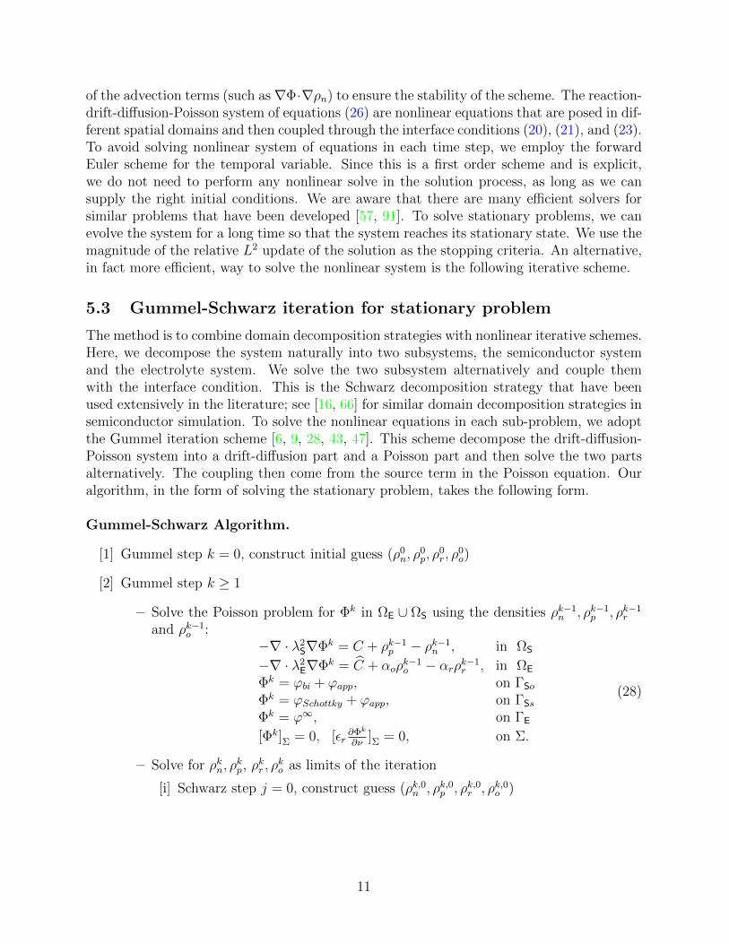
In this section, we present some numerical simulations for the semiconductor-electrolytesystem. For the simplicity of numerical implementation, we assume some symmetry in thesystem so that we can reduce the problem to one-dimension. We show in Fig. 2 two typicaltwo-dimensional systems where such dimension reductions can be performed. In the first
Σ
ES
EΓSΓΣS
E
EΓ
Figure 2: Two typical settings for semiconductor-electrolyte systems in dimension two. Thesemiconductor S and the electrolyte are separated by the interface Σ.
case, if we assume the system is invariant in the y-direction, then we have a one-dimensional
12
system in the x-direction. In the second setting, we have a radially symmetric system that isinvariant in the angular direction in the polar coordinate. The system can then be regardedas a one-dimensional system in the radial direction. The form of the semiconductor equationin polar coordinates is very similar to the original equations, except that the current termshave to be replaced by
∇ · Jn = −1
r
( ∂∂r
(Dnr∂ρn∂r
) +∂
∂θ(Dn
r
∂ρn∂θ
))
+1
r
( ∂∂r
(µnρnr∂Φ
∂r) +
∂
∂θ(µnρnr
∂Φ
∂θ)),
∇ · Jp = −1
r
( ∂∂r
(Dpr∂ρp∂r
) +∂
∂θ(Dp
r
∂ρp∂θ
))− 1
r
( ∂∂r
(µpρpr∂Φ
∂r) +
∂
∂θ(µpρpr
∂Φ
∂θ)).
(31)
where r and θ are the radial and angular variable respectively. Similar changes have to beapplied to the electrolyte equations as well. We omit these new expressions here to savespace.
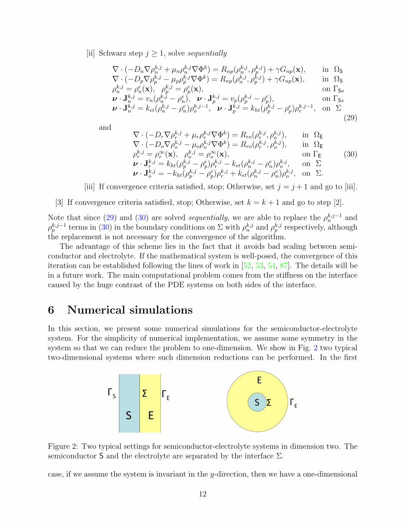
There are many physical parameters in the mathematical models that we have intro-duced. The values of many parameters depend on the materials used. We list in Tab. 1 thevalues that we use in the simulations. All those physical parameters can be tuned to morerealistic ones by careful calibration.
Parameter value unit Parameter value unitq 1.6× 10⁻¹⁹ [A s] kB 8.62× 10⁻⁵ q [J K−1]ε0 8.85× 10⁻¹⁴ [A s V−1 cm−1] εSr 11.9µn 1500 [cm2 V−1 s−1] µp 450 [cm2 V−1 s−1]τn 1× 10⁻⁶ [s] τp 1× 10⁻⁵ [s]An 2.8× 10⁻³¹ [cm6 s−1] Ap 9.9× 10⁻³² [cm6 s−1]Nc 2.80× 10¹⁹ [cm−3] Nv 1.04× 10¹⁹ [cm−3]vn 5× 10⁶ [cm s−1] vp 5× 10⁶ [cm s−1]Φm 2.4 [V] χ 1.2 [V]ket 1× 10⁻²¹ [cm4 s−1] kht 1× 10⁻¹⁷ [cm4 s−1]µo 2× 10⁻¹ [cm2 V−1 s−1] µr 0.5× 10⁻¹ [cm2 V−1 s−1]εEr 1000 G0 1.2× 10¹⁷ [cm−2s−1]
Table 1: Values of physical parameters used in the numerical simulations. The numbers aregiven in unit of cm, s, V, A. These are rough numbers taken from [3, 8, 42, 77, 90, 93] andreferences therein. Exact numbers for different materials can be found in these references.
To simplify the presentation, in all the simulations we have performed, we use an n-type semiconductor to construct the semiconductor-electrolyte system. The mathematicalframework we have presented and the numerical algorithm we coded, however, is not limitedto this case. We also select the electrolyte such that the charge numbers αr = αo = 1, andset the temperature of the system to be T = 300K.
The main quantities that we are interested in are densities of charges, electric field andcurrent through the system. The total current in the semiconductor part is J = Jn − Jp.From the drift-diffusion-Poisson equation (1), it is clear that when the system evolves intostationary state, ∇ · J = 0, which implies that J is constant in the semiconductor. Theequation (14) for the redox pair indicates that ∇ · (Jr + Jo) = 0 in stationary state. This
13

together with the fact that ν · (Jr + Jo) = 0 on Σ+ leads to the conclusion that Jr = −Join the electrolyte. The total current throughout the device is thus given us
J(x) =
Jn(x)− Jp(x), x ∈ S
Jr(x), x ∈ E(32)
We will perform simulations on two devices of different sizes:
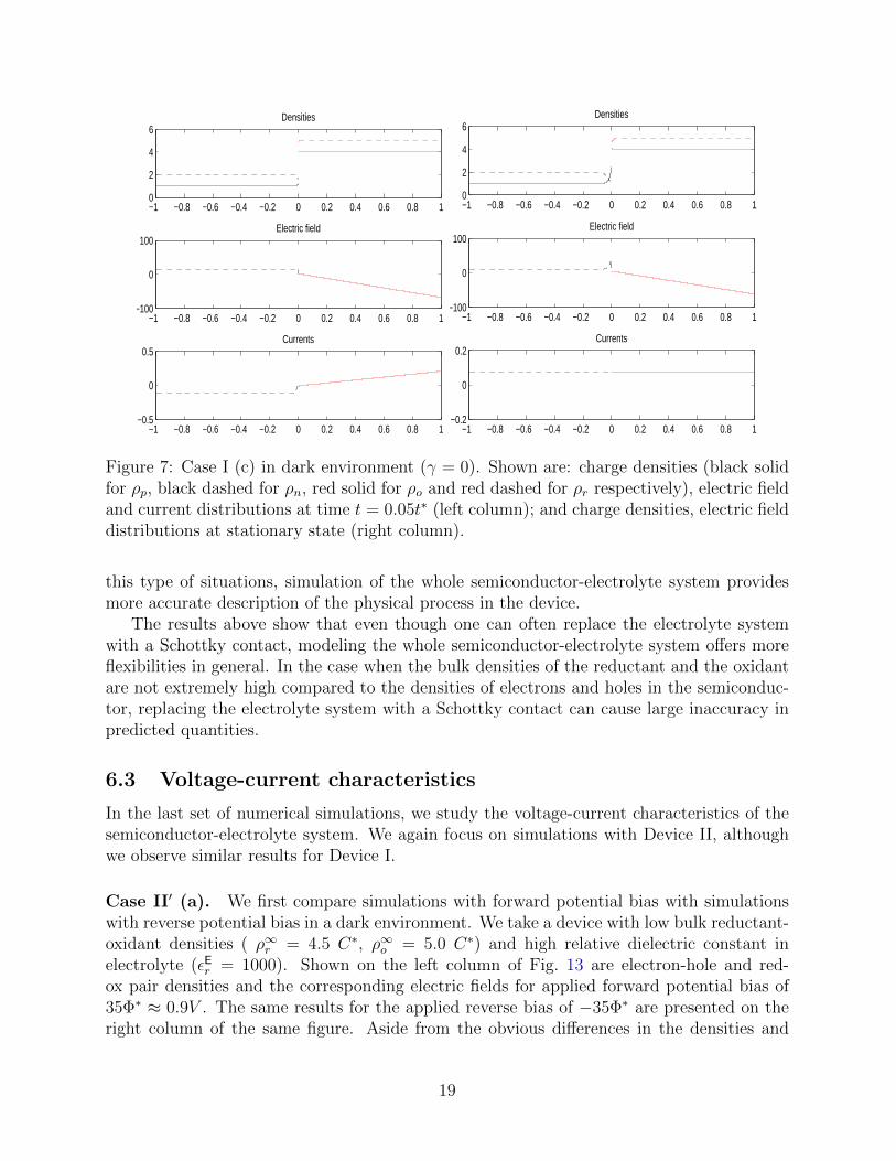
Device I. The device is contained in Ω = (−1.0l∗, 1.0l∗) with the semiconductor ΩS =(−1.0l∗, 0) and ΩE = (0, 1.0l∗) separated by the interface Σ located at x = 0. The semicon-ductor boundary ΓS is thus at the point x = −1.0l∗ while the electrolyte boundary ΓE is atthe point x = 1.0l∗.
Device II. The device is contained in Ω = (−0.2l∗, 0.2l∗) with the semiconductor ΩS =(−0.2l∗, 0) and ΩE = (0, 0.2l∗) separated by the interface Σ located at x = 0. The semicon-ductor boundary ΓS is thus at the point x = −0.2l∗ while the electrolyte boundary ΓE is atthe point x = 0.2l∗.
The two devices are designed to minimic a large (Device I) and small (Device II) nano-to-micro scale solar cell building blocks. We performance several simulations on each device.The setup for the simulations and the results are summarized in Tab. 2.
Case Device Summary
(a) I εEr = 1000, ρ∞r = 30.0C∗, ρ∞o = 29.0C∗,Fig. 3 (γ = 0)Fig. 4 (γ = 1)
I (b) I εEr = 1000, ρ∞r = 4.0C∗, ρ∞o = 5.0C∗,Fig. 5 (γ = 0)Fig. 6 (γ = 1)
(c) I εEr = 100, ρ∞r = 4.0C∗, ρ∞o = 5.0C∗,Fig. 7 (γ = 0)Fig. 8 (γ = 1)
(a) II εEr = 100, ρ∞r = 35.0C∗, ρ∞o = 30.0C∗, Figs. 9 & 10 (γ = 0)II
(b) II εEr = 100, ρ∞r = 2.0C∗, ρ∞o = 3.0C∗, Figs. 11 & 12 (γ = 1)
(a) II εEr = 1000, ρ∞r = 4.5C∗, ρ∞o = 5.0C∗,Fig. 13 (γ = 0)Fig. 14 (γ = 1)
II′
(b) II εEr = 1000, ρ∞r = 35.0C∗, ρ∞o = 30.0C∗, Fig. 15
Table 2: Summary of configurations for simulations performed in Section 6. In each group(I, II, or II′), we only list the parameters that are changed during different simulations ((a),(b) or (c)). Other general parameters are given in Tab. 1.
6.1 General dynamics of semiconductor-electrolyte systems
We now present simulation results on general dynamics of the semiconductor-electrolytesystems we constructed. We perform the simulations using the first system, i.e. Device I.
14
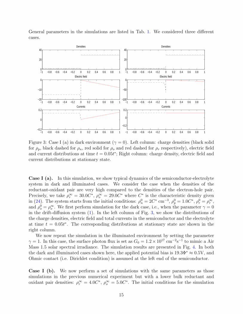
General parameters in the simulations are listed in Tab. 1. We considered three differentcases.
−1 −0.8 −0.6 −0.4 −0.2 0 0.2 0.4 0.6 0.8 10
20
40Densities
−1 −0.8 −0.6 −0.4 −0.2 0 0.2 0.4 0.6 0.8 1−20
−10
0Electric field
−1 −0.8 −0.6 −0.4 −0.2 0 0.2 0.4 0.6 0.8 1−0.2
0
0.2Currents
−1 −0.8 −0.6 −0.4 −0.2 0 0.2 0.4 0.6 0.8 10
20
40Densities
−1 −0.8 −0.6 −0.4 −0.2 0 0.2 0.4 0.6 0.8 1−100
−50
0Electric field
−1 −0.8 −0.6 −0.4 −0.2 0 0.2 0.4 0.6 0.8 1
−0.2
0
0.2Currents
Figure 3: Case I (a) in dark environment (γ = 0). Left column: charge densities (black solidfor ρp, black dashed for ρn, red solid for ρo and red dashed for ρr respectively), electric fieldand current distributions at time t = 0.05t∗; Right column: charge density, electric field andcurrent distributions at stationary state.
Case I (a). In this simulation, we show typical dynamics of the semiconductor-electrolytesystem in dark and illuminated cases. We consider the case when the densities of thereductant-oxidant pair are very high compared to the densities of the electron-hole pair.Precisely, we take ρ∞r = 30.0C∗, ρ∞o = 29.0C∗ where C∗ is the characteristic density givenin (24). The system starts from the initial conditions: ρ0
n = 2C∗ cm−3, ρ0p = 1.0C∗, ρ0
r = ρ∞r ,and ρ0
o = ρ∞o . We first perform simulation for the dark case, i.e., when the parameter γ = 0in the drift-diffusion system (1). In the left column of Fig. 3, we show the distributions ofthe charge densities, electric field and total currents in the semiconductor and the electrolyteat time t = 0.05t∗. The corresponding distributions at stationary state are shown in theright column.
We now repeat the simulation in the illuminated environment by setting the parameterγ = 1. In this case, the surface photon flux is set as G0 = 1.2×1017 cm−2s−1 to mimic a AirMass 1.5 solar spectral irradiance. The simulation results are presented in Fig. 4. In boththe dark and illuminated cases shown here, the applied potential bias is 19.3Φ∗ ≈ 0.5V, andOhmic contact (i.e. Dirichlet condition) is assumed at the left end of the semiconductor.
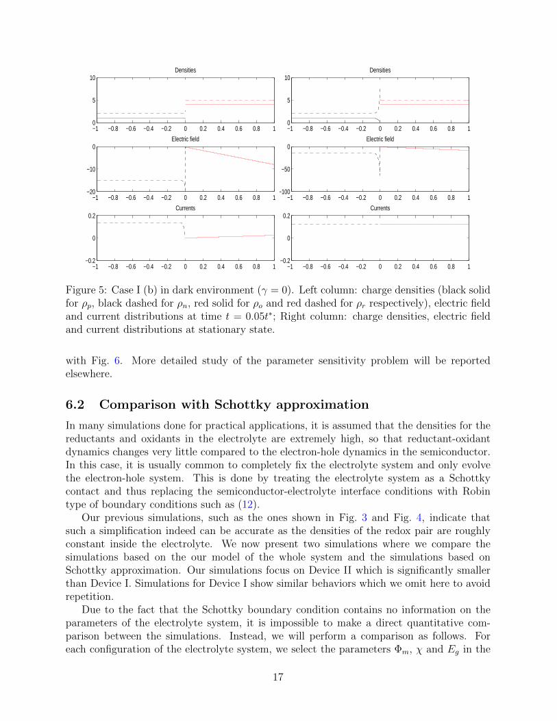
Case I (b). We now perform a set of simulations with the same parameters as thosesimulations in the previous numerical experiment but with a lower bulk reductant andoxidant pair densities: ρ∞r = 4.0C∗, ρ∞o = 5.0C∗. The initial conditions for the simulation
15

−1 −0.8 −0.6 −0.4 −0.2 0 0.2 0.4 0.6 0.8 10
20
40Densities
−1 −0.8 −0.6 −0.4 −0.2 0 0.2 0.4 0.6 0.8 1−20
−10
0Electric field
−1 −0.8 −0.6 −0.4 −0.2 0 0.2 0.4 0.6 0.8 1−0.2
0
0.2Currents
−1 −0.8 −0.6 −0.4 −0.2 0 0.2 0.4 0.6 0.8 10
20
40Densities
−1 −0.8 −0.6 −0.4 −0.2 0 0.2 0.4 0.6 0.8 1−100
−50
0Electric field
−1 −0.8 −0.6 −0.4 −0.2 0 0.2 0.4 0.6 0.8 1
−0.2
−0.1
0
0.1Currents
Figure 4: Case I (a) in illuminated environment (γ = 1). Left column: charge densities(black solid for ρp, black dashed for ρn, red solid for ρo and red dashed for ρr respectively),electric field and current distributions at time t = 0.05t∗; Right column: charge densities,electric field and current distributions at stationary state.
are: ρ0n = 2.5C∗, ρ0
p = 1.0C∗, ρ0r = ρ∞r and ρ0
o = ρ∞o . The results in the dark and theilluminated environments are shown in Fig. 5 and Fig. 6 respectively. We observe from thecomparison of Fig. 3 and Fig 4 with Fig. 5 and Fig. 6, that when all other factors are keptunchanged, lowering the density of the redox pair leads to significant change of the electricfield across the device, especially at the semiconductor-electrolyte interface. The chargedensities in the semiconductor also changes significantly. In both cases, however, the chargedensities in the electrolyte, however, remain as almost constant across the electrolyte. Thereare two reasons for this. First, the charge densities in the electrolyte are significantly higherthan those in the semiconductor (even in Case I (b)). Second, the relative dielectric constantof the electrolyte is much higher than that in the semiconductor, resulting in a relativelyconstant electric field inside the electrolyte. If we lower the relative dielectric function, weobserve a significant variation in charge density distributions in the electrolyte as we can seefrom the next numerical simulation.
Case I (c). There is a large number of physical parameters in the semiconductor-electrolytesystem that controls the dynamics of the system. To be specific, we show in this numeri-cal simulation the impact of relative dielectric constant in the electrolyte εEr on the systemperformance. The setup is exactly as in Case I (b) except that εEr = 100 now. We performsimulations in both the dark and illuminated environments. We plot in Fig. 7 the densities,the electric field and the current distributions at time t = 0.05t∗ and stationary state. Thecorresponding results for illuminated case are shown in Fig. 8. It is not hard to observe thedramatic change in all the quantities shown after comparing Fig. 7 with Fig. 5, and Fig. 8
16
−1 −0.8 −0.6 −0.4 −0.2 0 0.2 0.4 0.6 0.8 10
5
10Densities
−1 −0.8 −0.6 −0.4 −0.2 0 0.2 0.4 0.6 0.8 1−20
−10
0Electric field
−1 −0.8 −0.6 −0.4 −0.2 0 0.2 0.4 0.6 0.8 1−0.2
0
0.2Currents
−1 −0.8 −0.6 −0.4 −0.2 0 0.2 0.4 0.6 0.8 10
5
10Densities
−1 −0.8 −0.6 −0.4 −0.2 0 0.2 0.4 0.6 0.8 1−100
−50
0Electric field
−1 −0.8 −0.6 −0.4 −0.2 0 0.2 0.4 0.6 0.8 1−0.2
0
0.2Currents
Figure 5: Case I (b) in dark environment (γ = 0). Left column: charge densities (black solidfor ρp, black dashed for ρn, red solid for ρo and red dashed for ρr respectively), electric fieldand current distributions at time t = 0.05t∗; Right column: charge densities, electric fieldand current distributions at stationary state.
with Fig. 6. More detailed study of the parameter sensitivity problem will be reportedelsewhere.
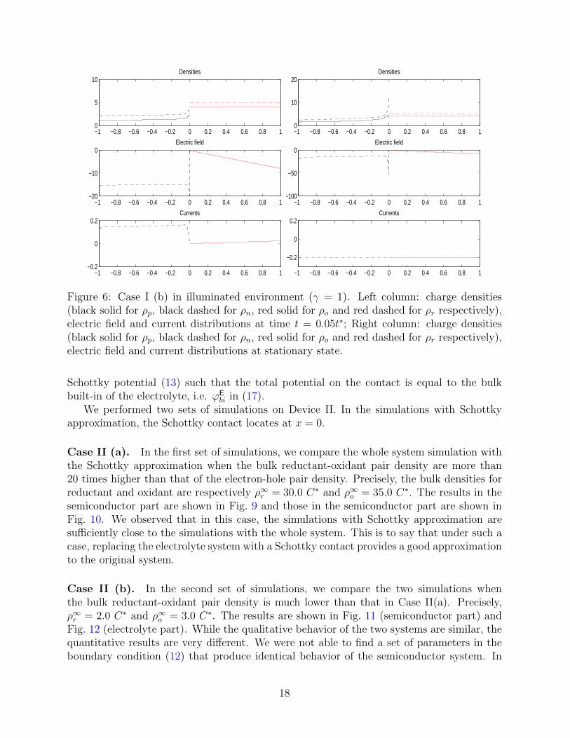
6.2 Comparison with Schottky approximation
In many simulations done for practical applications, it is assumed that the densities for thereductants and oxidants in the electrolyte are extremely high, so that reductant-oxidantdynamics changes very little compared to the electron-hole dynamics in the semiconductor.In this case, it is usually common to completely fix the electrolyte system and only evolvethe electron-hole system. This is done by treating the electrolyte system as a Schottkycontact and thus replacing the semiconductor-electrolyte interface conditions with Robintype of boundary conditions such as (12).
Our previous simulations, such as the ones shown in Fig. 3 and Fig. 4, indicate thatsuch a simplification indeed can be accurate as the densities of the redox pair are roughlyconstant inside the electrolyte. We now present two simulations where we compare thesimulations based on the our model of the whole system and the simulations based onSchottky approximation. Our simulations focus on Device II which is significantly smallerthan Device I. Simulations for Device I show similar behaviors which we omit here to avoidrepetition.
Due to the fact that the Schottky boundary condition contains no information on theparameters of the electrolyte system, it is impossible to make a direct quantitative com-parison between the simulations. Instead, we will perform a comparison as follows. Foreach configuration of the electrolyte system, we select the parameters Φm, χ and Eg in the
17
−1 −0.8 −0.6 −0.4 −0.2 0 0.2 0.4 0.6 0.8 10
5
10Densities
−1 −0.8 −0.6 −0.4 −0.2 0 0.2 0.4 0.6 0.8 1−20
−10
0Electric field
−1 −0.8 −0.6 −0.4 −0.2 0 0.2 0.4 0.6 0.8 1−0.2
0
0.2Currents
−1 −0.8 −0.6 −0.4 −0.2 0 0.2 0.4 0.6 0.8 10
10
20Densities
−1 −0.8 −0.6 −0.4 −0.2 0 0.2 0.4 0.6 0.8 1−100
−50
0Electric field
−1 −0.8 −0.6 −0.4 −0.2 0 0.2 0.4 0.6 0.8 1
−0.2
0
0.2Currents
Figure 6: Case I (b) in illuminated environment (γ = 1). Left column: charge densities(black solid for ρp, black dashed for ρn, red solid for ρo and red dashed for ρr respectively),electric field and current distributions at time t = 0.05t∗; Right column: charge densities(black solid for ρp, black dashed for ρn, red solid for ρo and red dashed for ρr respectively),electric field and current distributions at stationary state.
Schottky potential (13) such that the total potential on the contact is equal to the bulkbuilt-in of the electrolyte, i.e. ϕE
bi in (17).We performed two sets of simulations on Device II. In the simulations with Schottky
approximation, the Schottky contact locates at x = 0.
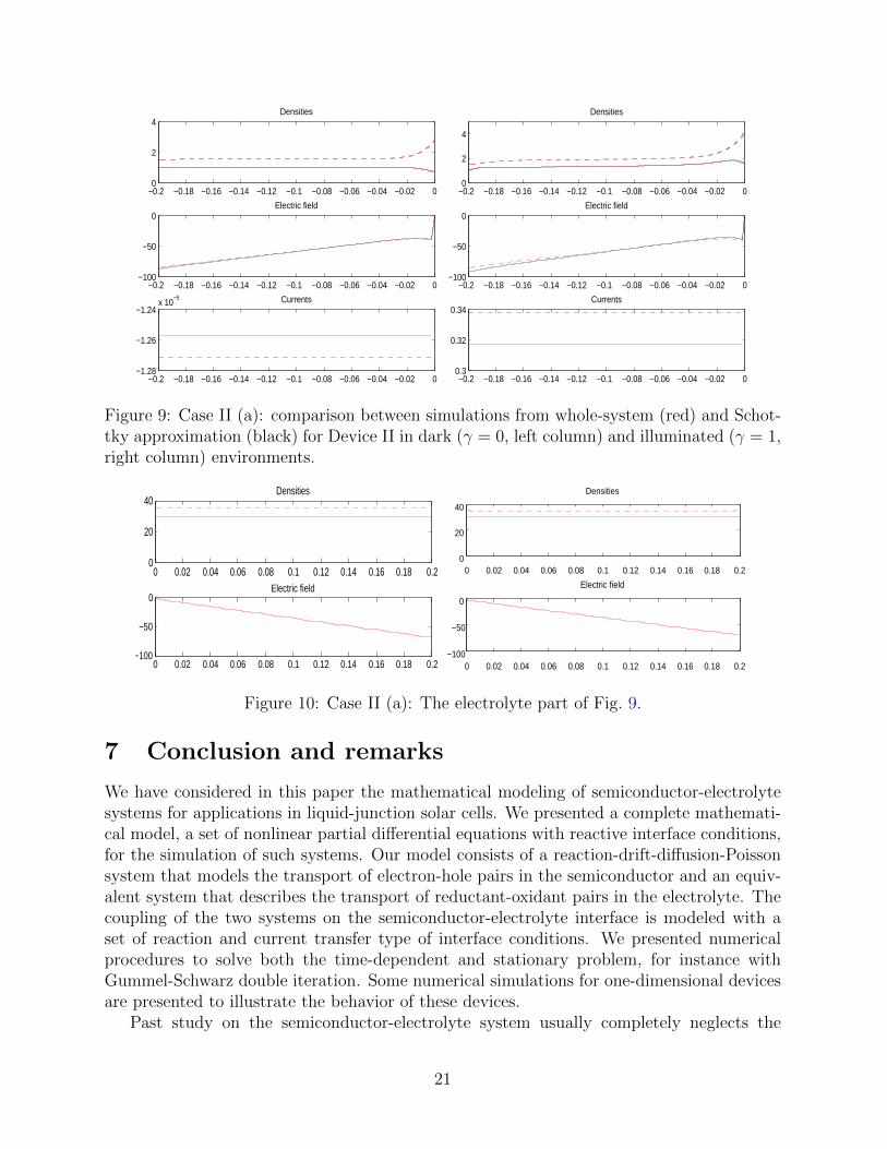
Case II (a). In the first set of simulations, we compare the whole system simulation withthe Schottky approximation when the bulk reductant-oxidant pair density are more than20 times higher than that of the electron-hole pair density. Precisely, the bulk densities forreductant and oxidant are respectively ρ∞r = 30.0 C∗ and ρ∞o = 35.0 C∗. The results in thesemiconductor part are shown in Fig. 9 and those in the semiconductor part are shown inFig. 10. We observed that in this case, the simulations with Schottky approximation aresufficiently close to the simulations with the whole system. This is to say that under such acase, replacing the electrolyte system with a Schottky contact provides a good approximationto the original system.
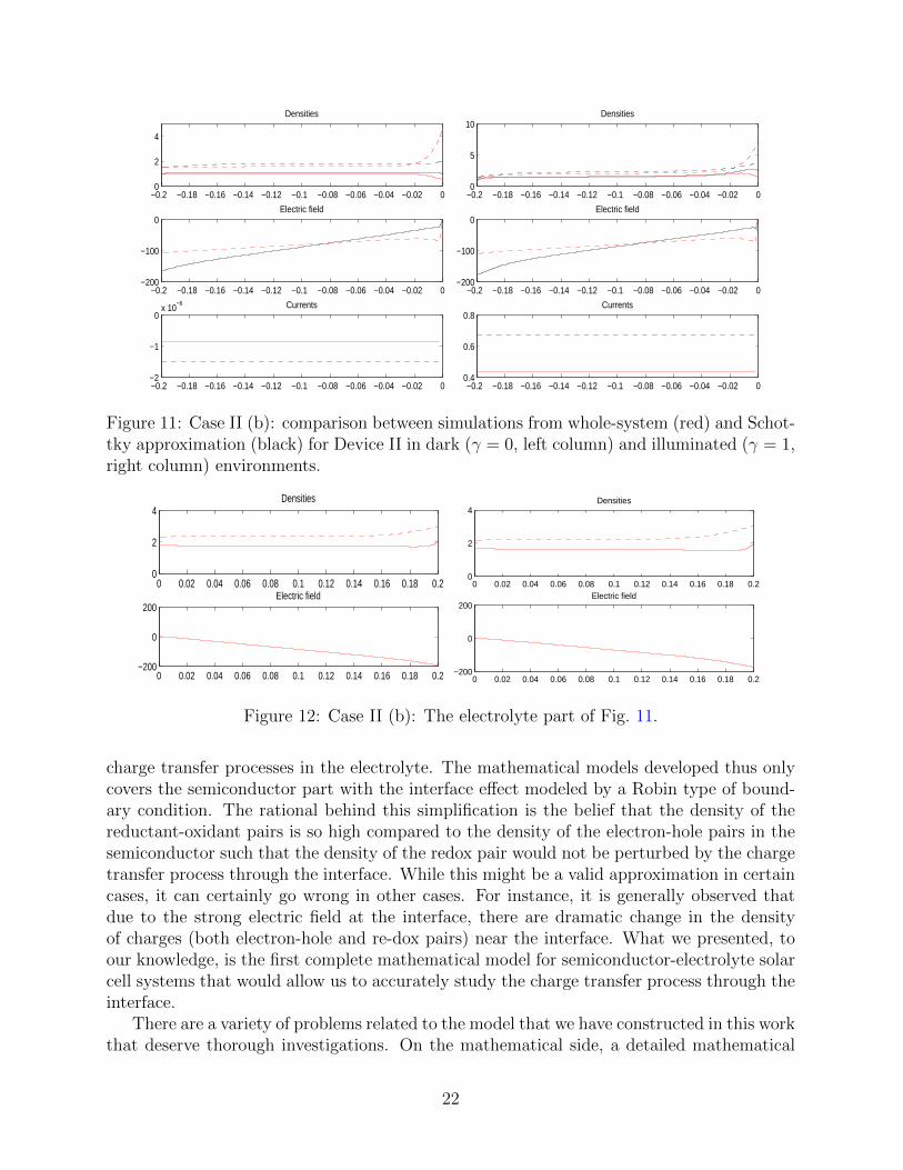
Case II (b). In the second set of simulations, we compare the two simulations whenthe bulk reductant-oxidant pair density is much lower than that in Case II(a). Precisely,ρ∞r = 2.0 C∗ and ρ∞o = 3.0 C∗. The results are shown in Fig. 11 (semiconductor part) andFig. 12 (electrolyte part). While the qualitative behavior of the two systems are similar, thequantitative results are very different. We were not able to find a set of parameters in theboundary condition (12) that produce identical behavior of the semiconductor system. In
18
−1 −0.8 −0.6 −0.4 −0.2 0 0.2 0.4 0.6 0.8 10
2
4
6Densities
−1 −0.8 −0.6 −0.4 −0.2 0 0.2 0.4 0.6 0.8 1−100
0
100Electric field
−1 −0.8 −0.6 −0.4 −0.2 0 0.2 0.4 0.6 0.8 1−0.5
0
0.5Currents
−1 −0.8 −0.6 −0.4 −0.2 0 0.2 0.4 0.6 0.8 10
2
4
6Densities
−1 −0.8 −0.6 −0.4 −0.2 0 0.2 0.4 0.6 0.8 1−100
0
100Electric field
−1 −0.8 −0.6 −0.4 −0.2 0 0.2 0.4 0.6 0.8 1−0.2
0
0.2Currents
Figure 7: Case I (c) in dark environment (γ = 0). Shown are: charge densities (black solidfor ρp, black dashed for ρn, red solid for ρo and red dashed for ρr respectively), electric fieldand current distributions at time t = 0.05t∗ (left column); and charge densities, electric fielddistributions at stationary state (right column).
this type of situations, simulation of the whole semiconductor-electrolyte system providesmore accurate description of the physical process in the device.
The results above show that even though one can often replace the electrolyte systemwith a Schottky contact, modeling the whole semiconductor-electrolyte system offers moreflexibilities in general. In the case when the bulk densities of the reductant and the oxidantare not extremely high compared to the densities of electrons and holes in the semiconduc-tor, replacing the electrolyte system with a Schottky contact can cause large inaccuracy inpredicted quantities.
6.3 Voltage-current characteristics
In the last set of numerical simulations, we study the voltage-current characteristics of thesemiconductor-electrolyte system. We again focus on simulations with Device II, althoughwe observe similar results for Device I.
Case II′ (a). We first compare simulations with forward potential bias with simulationswith reverse potential bias in a dark environment. We take a device with low bulk reductant-oxidant densities ( ρ∞r = 4.5 C∗, ρ∞o = 5.0 C∗) and high relative dielectric constant inelectrolyte (εEr = 1000). Shown on the left column of Fig. 13 are electron-hole and red-ox pair densities and the corresponding electric fields for applied forward potential bias of35Φ∗ ≈ 0.9V . The same results for the applied reverse bias of −35Φ∗ are presented on theright column of the same figure. Aside from the obvious differences in the densities and
19

−1 −0.8 −0.6 −0.4 −0.2 0 0.2 0.4 0.6 0.8 10
2
4
6Densities
−1 −0.8 −0.6 −0.4 −0.2 0 0.2 0.4 0.6 0.8 1−100
−50
0
50Electric field
−1 −0.8 −0.6 −0.4 −0.2 0 0.2 0.4 0.6 0.8 1−0.5
0
0.5Currents
−1 −0.8 −0.6 −0.4 −0.2 0 0.2 0.4 0.6 0.8 10
5
10Densities
−1 −0.8 −0.6 −0.4 −0.2 0 0.2 0.4 0.6 0.8 1−100
0
100Electric field
−1 −0.8 −0.6 −0.4 −0.2 0 0.2 0.4 0.6 0.8 1−0.2
0
0.2Currents
Figure 8: Case I (c) in illuminated environment (γ = 1). Shown are: charge densities (blacksolid for ρp, black dashed for ρn, red solid for ρo and red dashed for ρr respectively), electricfield and current distributions at time t = 0.05t∗ (left column); and charge densities, electricfield and current distributions at stationary state (right column).
electric field distributions, the currents through the system with forward and reverse biasesare very different, as can be seen later on Fig. 15.
The simulations are repeated in Fig. 14 in the illuminated environment. It is clear fromthe plots in Fig. 13 and Fig. 14, illumination changes dramatically the distribution of charges(and thus the electric field) inside the device as we have seen in the previous simulations.
Case II′ (b). We now attempt to explore the whole current-voltage (I-V) characteristicsof device II. To do that, we run the simulations for various different applied potentialsand compute the current through the system under each applied potential. We plot thecurrent data as a function of the applied potential to obtain the I-V curve of the system.The parameters are taken as ρ∞r = 35 C∗, ρ∞o = 30 C∗) and εEr = 1000 to mimic these inrealistic devices. We show in Fig. 15 the I-V curve obtained in both dark (line with stars)and illuminated (solid line with circles) environments. The applied potential bias lives inthe range [−1.5V, 1.9V ] which is roughly [−58.0Φ∗, 73.5Φ∗]. The currents, with the unitof 10−8qC
∗l∗
t∗= 1.6 mA cm−2. The maximum power voltage The intersections of the dash-
dotted vertical lines with the x-axis show the maximum power voltage (Φmp, red) and opencircuit voltage (Φoc, blue) respectively. The intersections of the dashed horizontal lines withthe y-axis show the maximum power current (Joc, red) and short circuit current (Jsc, blue)respectively.
20
−0.2 −0.18 −0.16 −0.14 −0.12 −0.1 −0.08 −0.06 −0.04 −0.02 00
2
4Densities
−0.2 −0.18 −0.16 −0.14 −0.12 −0.1 −0.08 −0.06 −0.04 −0.02 0−100
−50
0Electric field
−0.2 −0.18 −0.16 −0.14 −0.12 −0.1 −0.08 −0.06 −0.04 −0.02 0−1.28
−1.26
−1.24x 10
−5 Currents
−0.2 −0.18 −0.16 −0.14 −0.12 −0.1 −0.08 −0.06 −0.04 −0.02 00
2
4
Densities
−0.2 −0.18 −0.16 −0.14 −0.12 −0.1 −0.08 −0.06 −0.04 −0.02 0−100
−50
0Electric field
−0.2 −0.18 −0.16 −0.14 −0.12 −0.1 −0.08 −0.06 −0.04 −0.02 00.3
0.32
0.34Currents
Figure 9: Case II (a): comparison between simulations from whole-system (red) and Schot-tky approximation (black) for Device II in dark (γ = 0, left column) and illuminated (γ = 1,right column) environments.
0 0.02 0.04 0.06 0.08 0.1 0.12 0.14 0.16 0.18 0.20
20
40Densities
0 0.02 0.04 0.06 0.08 0.1 0.12 0.14 0.16 0.18 0.2−100
−50
0Electric field
0 0.02 0.04 0.06 0.08 0.1 0.12 0.14 0.16 0.18 0.2−2
0
2Currents
0 0.02 0.04 0.06 0.08 0.1 0.12 0.14 0.16 0.18 0.20
20
40
Densities
0 0.02 0.04 0.06 0.08 0.1 0.12 0.14 0.16 0.18 0.2−100
−50
0
Electric field
0 0.02 0.04 0.06 0.08 0.1 0.12 0.14 0.16 0.18 0.2−2
0
2
Currents
0 0.02 0.04 0.06 0.08 0.1 0.12 0.14 0.16 0.18 0.20
20
40Densities
0 0.02 0.04 0.06 0.08 0.1 0.12 0.14 0.16 0.18 0.2−100
−50
0Electric field
0 0.02 0.04 0.06 0.08 0.1 0.12 0.14 0.16 0.18 0.2−2
0
2Currents
0 0.02 0.04 0.06 0.08 0.1 0.12 0.14 0.16 0.18 0.20
20
40
Densities
0 0.02 0.04 0.06 0.08 0.1 0.12 0.14 0.16 0.18 0.2−100
−50
0
Electric field
0 0.02 0.04 0.06 0.08 0.1 0.12 0.14 0.16 0.18 0.2−2
0
2
CurrentsFigure 10: Case II (a): The electrolyte part of Fig. 9.
7 Conclusion and remarks
We have considered in this paper the mathematical modeling of semiconductor-electrolytesystems for applications in liquid-junction solar cells. We presented a complete mathemati-cal model, a set of nonlinear partial differential equations with reactive interface conditions,for the simulation of such systems. Our model consists of a reaction-drift-diffusion-Poissonsystem that models the transport of electron-hole pairs in the semiconductor and an equiv-alent system that describes the transport of reductant-oxidant pairs in the electrolyte. Thecoupling of the two systems on the semiconductor-electrolyte interface is modeled with aset of reaction and current transfer type of interface conditions. We presented numericalprocedures to solve both the time-dependent and stationary problem, for instance withGummel-Schwarz double iteration. Some numerical simulations for one-dimensional devicesare presented to illustrate the behavior of these devices.
Past study on the semiconductor-electrolyte system usually completely neglects the
21
−0.2 −0.18 −0.16 −0.14 −0.12 −0.1 −0.08 −0.06 −0.04 −0.02 00
2
4
Densities
−0.2 −0.18 −0.16 −0.14 −0.12 −0.1 −0.08 −0.06 −0.04 −0.02 0−200
−100
0Electric field
−0.2 −0.18 −0.16 −0.14 −0.12 −0.1 −0.08 −0.06 −0.04 −0.02 0−2
−1
0x 10
−6 Currents
−0.2 −0.18 −0.16 −0.14 −0.12 −0.1 −0.08 −0.06 −0.04 −0.02 00
5
10Densities
−0.2 −0.18 −0.16 −0.14 −0.12 −0.1 −0.08 −0.06 −0.04 −0.02 0−200
−100
0Electric field
−0.2 −0.18 −0.16 −0.14 −0.12 −0.1 −0.08 −0.06 −0.04 −0.02 00.4
0.6
0.8Currents
Figure 11: Case II (b): comparison between simulations from whole-system (red) and Schot-tky approximation (black) for Device II in dark (γ = 0, left column) and illuminated (γ = 1,right column) environments.
0 0.02 0.04 0.06 0.08 0.1 0.12 0.14 0.16 0.18 0.20
2
4Densities
0 0.02 0.04 0.06 0.08 0.1 0.12 0.14 0.16 0.18 0.2−200
0
200Electric field
0 0.02 0.04 0.06 0.08 0.1 0.12 0.14 0.16 0.18 0.2−2
0
2Currents
0 0.02 0.04 0.06 0.08 0.1 0.12 0.14 0.16 0.18 0.20
2
4Densities
0 0.02 0.04 0.06 0.08 0.1 0.12 0.14 0.16 0.18 0.2−200
0
200Electric field
0 0.02 0.04 0.06 0.08 0.1 0.12 0.14 0.16 0.18 0.2−2
0
2Currents
0 0.02 0.04 0.06 0.08 0.1 0.12 0.14 0.16 0.18 0.20
2
4Densities
0 0.02 0.04 0.06 0.08 0.1 0.12 0.14 0.16 0.18 0.2−200
0
200Electric field
0 0.02 0.04 0.06 0.08 0.1 0.12 0.14 0.16 0.18 0.2−2
0
2Currents
0 0.02 0.04 0.06 0.08 0.1 0.12 0.14 0.16 0.18 0.20
2
4Densities
0 0.02 0.04 0.06 0.08 0.1 0.12 0.14 0.16 0.18 0.2−200
0
200Electric field
0 0.02 0.04 0.06 0.08 0.1 0.12 0.14 0.16 0.18 0.2−2
0
2Currents
Figure 12: Case II (b): The electrolyte part of Fig. 11.
charge transfer processes in the electrolyte. The mathematical models developed thus onlycovers the semiconductor part with the interface effect modeled by a Robin type of bound-ary condition. The rational behind this simplification is the belief that the density of thereductant-oxidant pairs is so high compared to the density of the electron-hole pairs in thesemiconductor such that the density of the redox pair would not be perturbed by the chargetransfer process through the interface. While this might be a valid approximation in certaincases, it can certainly go wrong in other cases. For instance, it is generally observed thatdue to the strong electric field at the interface, there are dramatic change in the densityof charges (both electron-hole and re-dox pairs) near the interface. What we presented, toour knowledge, is the first complete mathematical model for semiconductor-electrolyte solarcell systems that would allow us to accurately study the charge transfer process through theinterface.
There are a variety of problems related to the model that we have constructed in this workthat deserve thorough investigations. On the mathematical side, a detailed mathematical
22

−0.2 −0.15 −0.1 −0.05 0 0.05 0.1 0.15 0.20
2
4
6Densities
−0.2 −0.15 −0.1 −0.05 0 0.05 0.1 0.15 0.2−80
−60
−40
−20
0
Electric field
−0.2 −0.15 −0.1 −0.05 0 0.05 0.1 0.15 0.20
2
4
6Densities
−0.2 −0.15 −0.1 −0.05 0 0.05 0.1 0.15 0.2
0
20
40
60
80Electric field
Figure 13: Case II′ (a) in dark (γ = 0) environment: comparison of charge densities (top)and the corresponding electric fields (bottom) in applied forward (left column) and reversed(right column) potential bias.
analysis on the well-posedness of the system is necessary. On the computational side, moredetailed numerical analysis of the model, including convergence of the Gummel-Schwarziteration, efficient high-order discretization and fast solution techniques, has to be studied.On the application side, it is important to calibrate the model parameters with experimentaldata that collected from real semiconductor-electrolyte solar cells. Once the aforementionedissues are addressed, we can use the model to help the design of more efficient solar cellsby for instance optimizing the various model parameters. We are currently investigatingseveral of these issues.
Acknowledgement
We would like to thank Professor Allen J. Bard and Charles B. Mullins for fruitful discussionson the current work. YH, IMG and HCL are supported by the NSF grants CHE 0934450and DMS-0807712. KR is supported by NSF grant DMS-0914825.
References
[1] F. Alabau, Structural properties of the one-dimensional drift-diffusion models forsemiconductors, Trans. Am. Math. Soc, 348 (1996), pp. 823–871.
[2] A. M. Anile, W. Allegretto, and C. Ringhofer, Mathematical Problems inSemiconductor Physics, Lecture Notes in Mathematics, Springer-Verlag, Berlin, 2003.
[3] A. J. Bard and L. R. Faulkner, Electrochemical methods: fundamentals and ap-plications, Wiley, second ed., 2000.
23

−0.2 −0.15 −0.1 −0.05 0 0.05 0.1 0.15 0.20
5
10
15Densities
−0.2 −0.15 −0.1 −0.05 0 0.05 0.1 0.15 0.2−80
−60
−40
−20
0
Electric field
−0.2 −0.15 −0.1 −0.05 0 0.05 0.1 0.15 0.20
2
4
6
8
10Densities
−0.2 −0.15 −0.1 −0.05 0 0.05 0.1 0.15 0.2
0
20
40
60
80Electric field
Figure 14: Case II′ (a) in illuminated (γ = 1) environment: comparison of charge densities(top) and the corresponding electric fields (bottom) in applied forward (left column) andreversed (right column) potential bias.
[4] S. Baumgartner and C. Heitzinger, A one-level FETI method for thedriftdiffusion-poisson system with discontinuities at an interface, J. Comput. Phys.,243 (2013), pp. 74–86.
[5] J. Bell, T. Farrell, M. Penny, and G. Will, A mathematical model of thesemiconductor-electrolyte interface in dye sensitised solar cells, in EMAC 2003 Pro-ceedings, R. May and W. F. Blyth, eds., University of Technology, Sydney, Australia,2003, Australian Mathematical Society, pp. 193–198.
[6] N. Ben Abdallah, M. J. Caceres, J. A. Carrillo, and F. Vecil, A deter-ministic solver for a hybrid quantum-classical transport model in nanoMOSFETs, J.Comput. Phys., 228 (2009), pp. 6553–6571.
[7] N. Ben Abdallah and P. Degond, On a hierarchy of macroscopic models forsemiconductors, J. Math. Phys., 37 (1996), pp. 3306–3333.
[8] K. F. Brennan, The Physics of Semiconductors : with Applications to OptoelectronicDevices, Cambridge University Press, New York, 1999.
[9] M. Burger and R. Pinnau, A globally convergent Gummel map for optimal dopantprofiling, Math. Models Methods Appl. Sci., 19 (2009), pp. 769–786.
[10] J. A. Carrillo, I. Gamba, and C.-W. Shu, Computational macroscopic approx-imations to the one-dimensional relaxation-time kinetic system for semiconductors,Physica D, 146 (2000), pp. 289–306.
[11] J. A. Carrillo, I. M. Gamba, A. Majorana, and C.-W. Shu, A WENO-solverfor the transients of Boltzmann-Poisson system for semiconductor devices: performanceand comparisons with Monte Carlo methods, J. Comput. Phys., 184 (2003), pp. 498–525.
24

−60 −40 −20 0 20 40 60 80−0.4
−0.3
−0.2
−0.1
0
0.1
0.2
0.3
Voltage [Φ*]
Cur
rent
[10
−8 q
C* l* / t
* ]
illuminated
dark
Figure 15: Case II′ (b): current-voltage (IV) curves for an n-type semiconductor-electrolytesystem in dark (dotted line with circles) and illuminated (solid line with dots) environments.The intersections of the dash-dotted vertical lines with the x-axis show the maximum powervoltage (Φmp, red) and open circuit voltage (Φoc, blue) respectively. The intersections ofthe dashed horizontal lines with the y-axis show the maximum power current (Joc, red) andshort circuit current (Jsc, blue) respectively.
[12] G. Cassano, C. de Falco, C. Giulianetti, and R. Sacco, Numerical simula-tion of tunneling effects in nanoscale semiconductor devices using quantum correcteddrift-diffusion models, Computer Methods in Applied Mechanics and Engineering, 195(2006), pp. 2193–2208.
[13] C. Cercignani, I. M. Gamba, and C. D. Levermore, High field approximationsto a Boltzmann-Poisson system and boundary conditions in a semiconductor, Appl.Math. Lett., 10 (1997), pp. 111–118.
[14] , A drift-collision balance asymptotic for a Boltzmann-Poisson system in boundeddomains, SIAM J. Appl. Math., 61 (2001), pp. 1932–1958.
[15] R.-C. Chen and J.-L. Liu, An accelerated monotone iterative method for thequantum-corrected energy transport model, J. Comput. Phys., 227 (2008), pp. 6226–6240.
[16] S. Chen, W. E, Y. Liu, and C.-W. Shu, A discontinuous galerkin implementation ofa domain decomposition method for kinetic-hydrodynamic coupling multiscale problemsin gas dynamics and device simulations, J. Comput. Phys., 225 (2007), pp. 1314–1330.
25

[17] Y. Cheng, I. Gamba, and K. Ren, Recovering doping profiles in semiconductordevices with the Boltzmann-Poisson model, J. Comput. Phys., 230 (2011), pp. 3391–3412.
[18] C. de Falco, M. Porro, R. Sacco, and M. Verri, Multiscale modeling andsimulation of organic solar cells, Comput. Methods Appl. Mech. Engrg., 245 (2012),pp. 102–116.
[19] C. de Falco, R. Sacco, and M. Verri, Analytical and numerical study of photocur-rent transients in organic polymer solar cells, Comput. Methods Appl. Mech. Engrg.,199 (2010), pp. 1722–1732.
[20] P. Degond and B. Niclot, Numerical analysis of the weighted particle method ap-plied to the semiconductor boltzmann equation, Numer. Math., 55 (1989), pp. 599–618.
[21] A. Deinega and S. John, Finite difference discretization of semiconductor drift-diffusion equations for nanowire solar cells, Computer Physics Communications, 183(2012), pp. 2128–2135.
[22] J. C. deMello, Highly convergent simulations of transport dynamics in organic light-emitting diodes, J. Comput. Phys., 181 (2002), pp. 564–576.
[23] C. R. Drago and R. Pinnau, Optimal dopant profiling based on energy-transportsemiconductor models, Math. Models Meth. Appl. Sci., 18 (2008), pp. 195–241.
[24] B. Eisenberg, Ionic channels: natural nanotubes described by the drift diffusion equa-tions, Superlattices and Microstructures, 27 (2000), pp. 545–549.
[25] W. R. Fawcett, Liquids, Solutions, and Interfaces: From Classical Macroscopic De-scriptions to Modern Microscopic Details, Oxford University Press, New York, 2004.
[26] F. Filbet and S. Jin, A class of asymptotic-preserving schemes for kinetic equationsand related problems with stiff sources, J. Comput. Phys., 229 (2010), pp. 7625–7648.
[27] J. M. Foley, M. J. Price, J. I. Feldblyum, and S. Maldonado, Analysis of theoperation of thin nanowire photoelectrodes for solar energy conversion, Energy Environ.Sci., 5 (2012).
[28] S. Gadau and A. Jungel, A three-dimensional mixed finite-element approximationof the semiconductor energy-transport equations, SIAM J. Sci. Comput., 31 (2008),pp. 1120–1140.
[29] M. Galler, Multigroup equations for the description of the particle transport in semi-conductors, World Scientific, 2005.
[30] Y. Q. Gao, Y. Georgievskii, and R. A. Marcus, On the theory of electrontransfer reactions at semiconductor electrode/liquid interfaces, J. Phys. Chem., 112(2000), pp. 3358–3369.
26
[31] Y. Q. Gao and R. A. Marcus, On the theory of electron transfer reactions atsemiconductor electrode/liquid interfaces. II. A free electron model, J. Phys. Chem.,112 (2000), pp. 6351–6360.
[32] A. Glitzky, Analysis of electronic models for solar cells including energy resolveddefect densities, Math. Methods Appl. Sci., 34 (2011), pp. 1980–1998.
[33] T. Grasser, ed., Advanced Device Modeling and Simulation, World Scientific Press,Singapore, 2003.
[34] H. Haug and A.-P. Jauho, Quantum Kinetics in Transport and Optics of Semicon-ductors, Springer-Verlag, Berlin, 1996.
[35] T. L. Horng, T. C. Lin, C. Liu, and B. Eisenberg, Pnp equations with stericeffects: a model of ion flow through channels, J Phys Chem B., 116 (2012), pp. 11422–11441.
[36] J. W. Jerome, Analysis of Charge Transport: A Mathematical Study of SemiconductorDevices, Springer-Verlag, Berlin, 1996.
[37] S. Jin and L. Pareschi, Discretization of the multiscale semiconductor boltzmannequation by diffusive relaxation schemes, J. Comput. Phys., 161 (2000), pp. 312–330.
[38] A. Jungel, Quasi-hydrodynamic Semiconductor Equations, Birkhauser, Basel, 2001.
[39] A. Jungel, Transport Equations for Semiconductors, Springer, Berlin, 2009.
[40] P. V. Kamat, K. Tvrdy, D. R. Baker, and J. G. Radich, Beyond photovoltaics:Semiconductor nanoarchitectures for liquid-junction solar cells, Chem. Rev., 110 (2010),pp. 6664–6688.
[41] B. M. Kayes, H. A. Atwater, and N. S. Lewis, Comparison of the device physicsprinciples of planar and radial p-n junction nanorod solar cells, J. Appl. Phys., 97(2005). 114302.
[42] R. Kircher and W. Bergner, Three-Dimensional Simulation of SemiconductorDevices, Berkhauser Verlag, Basel, 1991.
[43] A. A. Kulikovsky, A more accurate Scharfetter-Gummel algorithm of electron trans-port for semiconductor and gas discharge simulation, J. Comput. Phys., 119 (1995),pp. 149–155.
[44] D. Laser and A. J. Bard, Semiconductor electrodes: IX digital simulation of therelaxation of photogenerated free carriers and photocurrents, J. Electrochem. Soc.: Elec-trochemical Science and Technology, 123 (1976), pp. 1837–1842.
[45] , Semiconductor electrodes: VII digital simulation of charge injection and the es-tablishment of the space charge region in the absense of surface states, J. Electrochem.Soc.: Electrochemical Science and Technology, 123 (1976), pp. 1828–1832.
27
[46] , Semiconductor electrodes: VIII digital simulation of open-circuit photopotentials,J. Electrochem. Soc.: Electrochemical Science and Technology, 123 (1976), pp. 1828–1837.
[47] W. R. Lee, S. Wang, and K. L. Teo, An optimization approach to a finite dimen-sional parameter estimation problem in semiconductor device design, J. Comput. Phys.,156 (1999), pp. 241–256.
[48] N. S. Lewis, Photoeffects at the semiconductor/liquid interfaces, Ann. Rev. Mater.Sci., 14 (1984), pp. 95–117.
[49] , Mechanistic studies of light-induced charge separation at semiconductor/liquidinterfaces, Acc. Chem. Res., 23 (1990), pp. 176–183.
[50] , Progress in understanding electron-transfer reactions at semiconductor/liquid in-terfaces, J. Phys. Chem. B, 102 (1998), pp. 4843–4855.
[51] J. Li, C. Y., and Y. Liu, Mathematical simulation of metamaterial solar cells, Adv.Appl. Math. Mech., 3 (2011), pp. 702–715.
[52] P.-L. Lions, On the Schwarz alternating method. I., in First International Symposiumon Domain Decomposition Methods for Partial Differential Equations, SIAM, Philadel-phia, PA, 1988, pp. 1–42.
[53] , On the Schwarz alternating method. II. Stochastic interpretation and order prop-erties., in Domain Decomposition Methods, SIAM, Philadelphia, PA, 1989, pp. 47–90.
[54] , On the Schwarz alternating method. III. A variant for nonoverlapping subdo-mains., in Third International Symposium on Domain Decomposition Methods forPartial Differential Equations, SIAM, Philadelphia, PA, 1990, pp. 202–223.
[55] B. Liu, K. Nakata, X. Zhao, T. Ochiai, T. Murakami, and A. Fujishima, The-oretical kinetic analysis of heterogeneous photocatalysis: The effect of surface trappingand bulk recombination through defects, J. Phys. Chem. C, 115 (2011), pp. 16037–16042.
[56] W. Liu, One-dimensional steady-state PoissonNernstPlanck systems for ion channelswith multiple ion species, J. Diff. Eqn., 246 (2009), pp. 428–451.
[57] W.-C. Lo, L. Chen, M. Wang, and Q. Nie, A robust and efficient method for steadystate patterns in reactiondiffusion systems, J. Comput. Phys., 231 (2012), pp. 5062–5077.
[58] B. Lu, M. J. Holst, J. A. McCammon, and Y. C. Zhou, Poissonnernstplanckequations for simulating biomolecular diffusionreaction processes I: Finite element so-lutions, J. Comput. Phys., 229 (2010), pp. 6979–6994.
[59] B. Lu and Y. C. Zhou, Poisson-Nernst-Planck equations for simulating biomoleculardiffusion-reaction processes II: Size effects on ionic distributions and diffusion-reactionrates, Biophysical Journal, 100 (2011), pp. 2475–2485.
28
[60] S. Mafe, J. Pellicer, and V. M. Aguilella, A numerical approach to ionictransport through charged membranes, J. Comput. Phys., 75 (1988), pp. 1–14.
[61] A. Majorana and R. Pidatella, A finite difference scheme solving the Boltzmann-Poisson system for semiconductor devices, J. Comput. Phys., 174 (2001), pp. 649–668.
[62] J. C. Manifacier, Multiple steady state currentvoltage characteristics in driftdiffu-sion modelisation of N type and semi-insulating GaAs Gunn structures, Solid-StateElectronics, 54 (2010), pp. 1511–1519.
[63] P. A. Markowich, C. A. Ringhofer, and C. Schmeiser, Semiconductor Equa-tions, Springer, New York, 1990.
[64] S. R. Mathur and J. Y. Murthy, A multigrid method for the PoissonNernstPlanckequations, International Journal of Heat and Mass Transfer, 52 (2009), pp. 4031–4039.
[65] R. Memming, Semiconductor electrochemistry, Wiley-VCH, 2001.
[66] S. Micheletti, A. Quarteroni, and R. Sacco, Current-voltage characteristicssimulation of semiconductor devices using domain decomposition, J. Comput. Phys.,119 (1995), pp. 46–61.
[67] B. Niclot, P. Degond, and F. Poupaud, Deterministic particle simulations of theBoltzmann transport equation of semiconductors, J. Comput. Phys., 78 (1988), pp. 313–349.
[68] A. J. Nozik and R. Memming, Physical chemistry of semiconductor-liquid interfaces,J. Phys. Chem., 100 (1996), pp. 13061–13078.
[69] M. E. Orazem and J. Newman, Mathematical modeling of liquid-junction photo-voltaic cells I. governing equations, J. Electrochem. Soc., 131 (1984), pp. 2569–2574.
[70] , Mathematical modeling of liquid-junction photovoltaic cells II. effect of systemparameters on current-potential curves, J. Electrochem. Soc., 131 (1984), pp. 2574–2582.
[71] , Mathematical modeling of liquid-junction photovoltaic cells III. optimization ofcell configurations, J. Electrochem. Soc., 131 (1984), pp. 2582–2589.
[72] M. Penny, T. Farrell, and C. Please, A mathematical model for interfacialcharge transfer at the semiconductor-dye-electrolyte interface of a dye-sensitised solarcell, Solar Energy Materials and Solar Cells, 92 (2008), pp. 11–23.
[73] M. A. Penny, T. W. Farrell, G. D. Will, and J. M. Bell, Modelling interfacialcharge transfer in dye-sensitised solar cells, J. Photochem. Photobiol. A, 164 (2004),pp. 41–46.
[74] G. Richardson, C. Please, J. Foster, and J. Kirkpatrick, Asymptotic solutionof a model for bilayer organic diodes and solar cells, SIAM J. Appl. Math., 72 (2012),pp. 1792–1817.
29
[75] C. A. Ringhofer, Computational methods for semiclassical and quantum transportin semiconductor devices, Acta Numer., 6 (1997), pp. 485–521.
[76] A. Rossani, A new derivation of the driftdiffusion equations for electrons and phonons,Physica A: Statistical Mechanics and its Applications, 390 (2011), pp. 223–230.
[77] A. Schenk, Advanced Physical Models for Silicon Device Simulation, Springer-Verlag,Wien, 1998.
[78] D. Schroeder, Modelling of Interface Carrier Transport for Device Simulation,Springer-Verlag, Wien, 1994.
[79] Z. Schuss, B. Nadler, and R. S. Eisenberg, Derivation of PNP equations in bathand channel from a molecular model, Phys. Rev. E, 64 (2001). 036116.
[80] S. Selberherr, Analysis and Simulation of Semiconductor Devices, Springer-Verlag,Vienna, Austria, 1984.
[81] N. Seoane, A. J. Garcıa-Loureiro, K. Kalna, and A. Asenov, Impact ofintrinsic parameter fluctuations on the performance of HEMTs studied with a 3d paralleldrift-diffusion simulator, Solid-State Electronics, 51 (2007), pp. 481–488.
[82] S. Sho and S. Odanaka, A quantum energy transport model for semiconductor devicesimulation, J. Comput. Phys., 235 (2013), pp. 486–496.
[83] A. Singer and J. Norbury, A Poisson-Nernst-Planck model for biological ionchannels– An asymptotic analysis in a 3-D narrow funnel, European J. Appl. Math.,19 (2008), pp. 541–560.
[84] D. Singh, X. Guo, J. Y. Murthy, A. Alexeenko, and T. Fisher, Modelingof subcontinuum thermal transport across semiconductor-gas interfaces, J. Appl. Phys.,106 (2009). 024314.
[85] H. Steinruck, A bifurcation analysis of the one-dimensional steady-state semiconduc-tor device equations, SIAM J. Appl. Math., 49 (1989), pp. 1102–1121.
[86] P. Thum, T. Clees, G. Weyns, G. Nelissen, and J. Deconinck, Efficientalgebraic multigrid for migrationdiffusionconvectionreaction systems arising in electro-chemical simulations, J. Comput. Phys., 229 (2010), pp. 7260–7276.
[87] A. Toselli and O. B. Widlund, Domain Decomposition Methods - Algorithms andTheory, Springer-Verlag, 2005.
[88] M. J. Ward, L. G. Reyna, and F. M. Odeh, Multiple steady-state solutions in amultijunction semiconductor device, SIAM J. Appl. Math., 51 (1991), pp. 90–123.
[89] Y. Yamada, Energy transport drift-diffusion model for submicrometer GaAs MES-FETs, Microelectronics Journal, 28 (1997), pp. 561–569.
30
[90] P. Y. Yu and M. Cardona, Fundamentals of Semiconductors: Physics and MaterialsProperties, Springer, Berlin, 3rd ed., 2003.
[91] S. Zhao, J. Ovadia, X. Liu, Y.-T. Zhang, and Q. Nie, Operator splitting im-plicit integration factor methods for stiff reactiondiffusionadvection systems, J. Comput.Phys., 230 (2011), pp. 5996–6009.
[92] Q. Zheng, D. Chen, and G.-W. Wei, Second-order PoissonNernstPlanck solver forion transport, J. Comput. Phys., 230 (2011), pp. 5239–5262.
[93] H. Zhu, Experimental and theoretical aspects of electrode/electrolyte interfaces, PhDthesis, Case Western Reserve University, Cleveland, Ohio, 2010.
31