Embed Size (px)
Citation preview

On the modelling of linear-assisted DC-DC voltage regulators for photovoltaic solar energy systems
Herminio Martínez-García1,*, and Encarna García-Vílchez1
1Eastern Barcelona School of Engineering (Escola d’Enginyeria de Barcelona Est, EEBE), Department of Electronics Engineering, Tech. University of Catalonia (UPC – BarcelonaTech), Diagonal-Besòs Campus. Eduard Maristany Ave., nº 10 – 14, E-08019 – Barcelon, Spain
Abstract. This paper shows the modelling of linear–assisted or hybrid (linear & switching) DC/DC voltage regulators. In this kind of regulators, an auxiliary linear regulator is used, which objective is to cancel the ripple at the output voltage and provide fast responses for load variations. On the other hand, a switching DC/DC converter, connected in parallel with the linear regulator, allows to supply almost the whole output current demanded by the load. The objective of this topology is to take advantage of the suitable regulation characteristics that series linear voltage regulators have, but almost achieving the high efficiency that switching DC/DC converters provide. Linear-assisted DC/DC regulators are feedback systems with potential instability. Therefore, their modelling is mandatory in order to obtain design guidelines and assure stability of the implemented power supply system.
1 Introduction Series linear regulators have been structures widely used in power supply systems for decades, providing supplies with low or moderate currents and consume [1–2]. This kind of voltage regulators has several advantages that lead their use. However, in spite of these advantages, linear regulators suffer from some serious drawbacks. As a result, they are not recommendable in some supply systems, especially for high power.
The alternative, DC/DC switching converters [3–4], has evident advantages opposite to linear regulators. However, the design and implementation of this sort of converters is a more complex process than in linear regulators, especially their control loops when both line and load regulations are desired. Furthermore, the intrinsic switched nature of these converters produces ripples in the output voltage and an increment of the EMIs in neighbouring electronic systems.
The use of linear-assisted hybrid DC/DC voltage regulators takes advantages of previous alternatives [5–7]. Apart from this, some of the aforementioned drawbacks are minimized as, for instance, the low efficiency and the high power dissipation in linear regulators, or the complexity in the design of the control for switching converters. Among
* Corresponding author: [email protected]
© The Authors, published by EDP Sciences. This is an open access article distributed under the terms of the Creative Commons Attribution License 4.0 (http://creativecommons.org/licenses/by/4.0/).
DOI: 10.1051/e3sconf/20172200113E3S Web of Conferences 22, 00113 (2017)AUTHOR'S DRAFT

other applications, this kind of voltage regulators can be of interest in modern high-efficiency battery chargers.
In this article, a proposal of variable frequency linear–assisted hybrid DC/DC regulator (or linear-switching hybrid DC/DC regulator) and its modelling is presented. The system has a control loop to maintain a constant output voltage that could induce instabilities as a function of the values of the circuit components and the values of the load (in a similar way that linear regulators). Thus a stability study is necessary to obtain design guidelines for this kind of DC/DC voltage regulators and assure the stability of the implemented power supply system.
2 Structure of a linear-assisted DC/DC voltage regulator
The proposed configuration of a linear-assisted DC/DC voltage regulator makes use of an analogue comparator that controls the conduction or cut of the transistor Q1, just as it can be seen in Fig. 1, and fixes the switching frequency. Note that the objective of the switching converter is to provide the excess of current that the linear regulator does not supply. Consequently:
( ) ( )out reg LI i t i t (1)
Vout
Vin
ireg(t)
Iout
iL(t)
VC
D1
Q1
CMP1
L1
ireg(t)
RL
Rlim
Vref
+
–
+–
Driver
Voltage Linear Regulator
Fig. 1. Basic structure of a linear-assisted DC/DC voltage regulator or self-switched hybrid regulator that supplies a load RL.
Just not considering in a first approximation any hysteresis in the analogue comparator CMP1, the operation of the circuit is just as it is explained as follows: if the load current is below a boundary current value, that we name as threshold switching current, Iγ, the output of CMP1 is held low. Thus the switching converter will be disabled and IL will be zero. As a result, the linear regulator supplies the load RL, providing all the output current (that is, Ireg = Iout).
However, in the moment that load current increases and goes slightly beyond this limit current Iγ, the comparator output will pass to high level, increasing IL in a linear form. Taking into account expression (1) and that the load current is constant (equal to Vout/RL), ireg(t) will tend to decrease also linearly (Fig. 2), just reaching a value below Iγ. In this moment, the comparator changes its output from high to low level, cutting Q1 and forcing IL to decrease. Then, when the current in the inductance decreases to a value in which ireg(t)>Iγ, the comparator changes from low to high level, repeating the cycle again.
2
DOI: 10.1051/e3sconf/20172200113E3S Web of Conferences 22, 00113 (2017)

other applications, this kind of voltage regulators can be of interest in modern high-efficiency battery chargers.
In this article, a proposal of variable frequency linear–assisted hybrid DC/DC regulator(or linear-switching hybrid DC/DC regulator) and its modelling is presented. The systemhas a control loop to maintain a constant output voltage that could induce instabilities asa function of the values of the circuit components and the values of the load (in a similarway that linear regulators). Thus a stability study is necessary to obtain design guidelinesfor this kind of DC/DC voltage regulators and assure the stability of the implementedpower supply system.
2 Structure of a linear-assisted DC/DC voltage regulatorThe proposed configuration of a linear-assisted DC/DC voltage regulator makes use of an analogue comparator that controls the conduction or cut of the transistor Q1, just as it can be seen in Fig. 1, and fixes the switching frequency. Note that the objective of the switchingconverter is to provide the excess of current that the linear regulator does not supply.Consequently:
( ) ( )out reg LI i t i t (1)
Vout
Vin
ireg(t)
Iout
iL(t)
VC
D1
Q1
CMP1
L1
ireg(t)
RL
Rlim
Vref
+
–
+–
Driver
Voltage LinearRegulator
Fig. 1. Basic structure of a linear-assisted DC/DC voltage regulator or self-switched hybrid regulator that supplies a load RL.
Just not considering in a first approximation any hysteresis in the analogue comparatorCMP1, the operation of the circuit is just as it is explained as follows: if the load current isbelow a boundary current value, that we name as threshold switching current, Iγ, the outputof CMP1 is held low. Thus the switching converter will be disabled and IL will be zero. As a result, the linear regulator supplies the load RL, providing all the output current (that is,Ireg = Iout).
However, in the moment that load current increases and goes slightly beyond this limitcurrent Iγ, the comparator output will pass to high level, increasing IL in a linear form.Taking into account expression (1) and that the load current is constant (equal to Vout/RL), ireg(t) will tend to decrease also linearly (Fig. 2), just reaching a value below Iγ. In this moment, the comparator changes its output from high to low level, cutting Q1 and forcingIL to decrease. Then, when the current in the inductance decreases to a value in whichireg(t)>Iγ, the comparator changes from low to high level, repeating the cycle again.
Vref and Rlim determine the value of the threshold switching current Iγ according to Rlim=Vref/Iγ. With the objective of reducing the value of the dissipated power by the internal transistor of the linear regulator to the utmost, this current Iγ has to be the minimum and necessary in order to make the linear regulator work properly, without penalizing its good regulation characteristics. It will also increase the efficiency of the system, even with significant load currents.
iL(t)
ireg(t) I
TON TOFF
Iout
Fig. 2. Currents flowing through RL, inductance L1 and linear regulator in the steady state of the linear-assisted DC/DC voltage regulator shown in Fig. 1.
The delays of the electronic circuits determine a little hysteresis that limits the maximum value of the switching frequency. Nevertheless, with the objective of fixing the maximum value of this switching frequency to a suitable value, it is convenient to add a hysteresis to CMP1.
A practical implementation of the self–switched hybrid regulator presented in Fig. 1 can be found in [8]. Fig. 3 shows the transient of a variable-frequency linear-assisted voltage regulator with Vin = 10 V. Having into account that the upper and lower switching threshold levels of the comparator (Schmitt trigger) are VH and VL, respectively, the switching frequency is given by:
lim
1
1out out
H L in
V VRfL V V V
(2)
vin(t)
vd(t)
vout(t)=Vout
ireg(t) iL(t)
Iout
Fig. 3. Transient response of the variable-frequency linear-assisted voltage regulator with Vin = 10 V. It can be seen the response of the circuit to an input step from 10 V to 13 V in t = 20 μs, and when there is a decrement of the load resistance from 10 Ω to 5 Ω in t = 40 μs.
3
DOI: 10.1051/e3sconf/20172200113E3S Web of Conferences 22, 00113 (2017)
3 Modelling of linear-assisted DC/DC voltage regulators
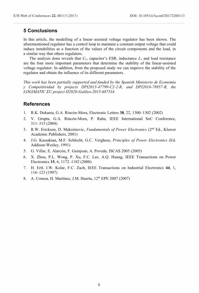
It is important to highlight that in previous discussion the effect of an output capacitance has not been considered. Effectively, these linear–assisted voltage regulators work properly when the load capacitance is null. In spite of this, some capacitance can be suitable in order to eliminate possible transitory peaks in the output voltage when the regulator supplies variable loads (that is, high slew–rate in the output current). This output capacitor improves the response of the converter appreciably. However, the effect of an output capacitor in parallel with the load, a parasitic output capacitance or a capacitance load induces a trend to instability. These instabilities produce and important and considerable increment of the output-ripple around the desired average output voltage that is observed in linear-assisted voltage regulators.
Fig. 4 shows a transient response of the linear-assisted voltage regulator in the same conditions that Fig. 3 but with an output capacitance CL = 100 nF and an equivalent series resistance (ESR) equal to 10 mΩ. Note that, with these conditions, expression (1) is not satisfied due to the inclusion of the CL network. As a consequence, the obtained waveforms in the circuit are not as the reflected in Fig. 3. In addition, the current ireg(t) increases and thus the efficiency of the regulator is reduced significantly.
Time
0s 5us 10us 15us 20us 25us 30us 35us 40us 45us 50us 55us 60usI(L1) I(RL1) IC(Q1b)
0A
1.0A
2.0AV(VCC) V(D1:2) V(Vout)
0V
5V
10V
15V
SEL>>
vin(t)
vd(t)
vout(t)=Vout
ireg(t) iL(t) Iout
Fig. 4. Transient response of the linear–assisted voltage regulator with an output capacitance CL = 100 nF. It can be seen the response of the circuit to an input step from 10 V to 13 V in t = 20 μs, and when there is a decrement of the load resistance from 10 Ω to 5 Ω in t = 40 μs.
Therefore, the CL has to be an agreement value. This value must be high enough but providing stability of the supply system. Even more, the authors have observed that in a linear-assisted voltage regulator, the frequency response of the system (and thus the stability conditions) is highly sensitive to the load conditions and the output capacitor connected (or parasitic capacitance existing) in parallel with the load resistor. Some parameters determine the aforementioned instabilities. However, the most important are the values of the output capacitance CL, its equivalent series resistance, the load resistor RL and the inductor L1.
4
DOI: 10.1051/e3sconf/20172200113E3S Web of Conferences 22, 00113 (2017)

3 Modelling of linear-assisted DC/DC voltage regulatorsIt is important to highlight that in previous discussion the effect of an output capacitance has not been considered. Effectively, these linear–assisted voltage regulators work properlywhen the load capacitance is null. In spite of this, some capacitance can be suitable in orderto eliminate possible transitory peaks in the output voltage when the regulator supplies variable loads (that is, high slew–rate in the output current). This output capacitor improves the response of the converter appreciably. However, the effect of an output capacitor inparallel with the load, a parasitic output capacitance or a capacitance load induces a trend toinstability. These instabilities produce and important and considerable increment of theoutput-ripple around the desired average output voltage that is observed in linear-assistedvoltage regulators.
Fig. 4 shows a transient response of the linear-assisted voltage regulator in the sameconditions that Fig. 3 but with an output capacitance CL = 100 nF and an equivalent series resistance (ESR) equal to 10 mΩ. Note that, with these conditions, expression (1) is notsatisfied due to the inclusion of the CL network. As a consequence, the obtained waveformsin the circuit are not as the reflected in Fig. 3. In addition, the current ireg(t) increases andthus the efficiency of the regulator is reduced significantly.
Time
0s 5us 10us 15us 20us 25us 30us 35us 40us 45us 50us 55us 60usI(L1) I(RL1) IC(Q1b)
0A
1.0A
2.0AV(VCC) V(D1:2) V(Vout)
0V
5V
10V
15V
SEL>>
vin(t)
vd(t)
vout(t)=Vout
ireg(t)iL(t)Iout
Fig. 4. Transient response of the linear–assisted voltage regulator with an output capacitance CL = 100 nF. It can be seen the response of the circuit to an input step from 10 V to 13 V in t = 20 μs,and when there is a decrement of the load resistance from 10 Ω to 5 Ω in t = 40 μs.
Therefore, the CL has to be an agreement value. This value must be high enough butproviding stability of the supply system. Even more, the authors have observed that in a linear-assisted voltage regulator, the frequency response of the system (and thus the stability conditions) is highly sensitive to the load conditions and the output capacitorconnected (or parasitic capacitance existing) in parallel with the load resistor. Someparameters determine the aforementioned instabilities. However, the most important are the values of the output capacitance CL, its equivalent series resistance, the load resistor RL and the inductor L1.
All these points make necessary to analyze the regulator in order to obtain design approaches that guarantees its stability. The model of the linear-assisted DC/DC voltage regulator is presented in Fig. 5. For the operational amplifier is considered its low-pass response in block H1, with a differential gain (Ad) and a dominant pole (O), and its output resistance (roa). For transistor (working in its linear zone) is considered the base-emitter dynamic resistance (r) and a current gain (β). Thus the block H2 contains only the association of resistors roa and r.
Fig. 5. Proposed model of the linear-assisted DC/DC voltage regulator.
The r value is calculated as usual from equation (3):
be T
b Cq
dv vrdi I
(3)
The kd block makes sense of collector current and obtain the conducting ratio of switching transistor as equation (4).
,max
1d
c c
dki i
(4)
The inductor small signal voltage is vi and defined as usual:
i ov d E e D v (5)
The inductor current (iL in Fig. 5) is obtained thanks to the voltage vi and the block H3, which models the inductor and its series resistance. Finally, with output current (iout) and block H4, the output voltage (vo) is obtained. In the block H4 the load resistance and output capacitor with its ESR is modelled.
In Fig. 6 is presented the flow graph of the modelled linear–assisted voltage regulator. Applying the Mason rule we obtain the transfer function given by:
svsvsG
ref
o (6)
In table 1 the Maple® code is presented in order to obtain the transfer function of equation (6). Subsequent to this, the result is simulated with Matlab® to obtain the poles zeros map of the system (pzmap function). The used simulation values are close to the experimental values of the implemented prototype (table 2).
5
DOI: 10.1051/e3sconf/20172200113E3S Web of Conferences 22, 00113 (2017)

Fig. 6. Proposed model of the linear-assisted DC/DC voltage regulator.
Table 1. Maple® code used to obtain the transfer function given in equation (6) for the linear-assisted DC/DC voltage regulator.
restart; H1:=Aoa/(1+s/woa); H2:=1/(roa+rd); H3:=1/(rl+s*L); H4:=R*(1/C/s+rc)/(R+1/C/s+rc); P1:=H1*H2*beta*kd*E*H3*H4; A1:=1; P2:=H1*H2*beta*H4; A2:=1;
L1:=-H3*H4; L2:=-H2*beta*kd*E*H3*H4; L3:=-H2*beta*H4; L4:=-H1*H2*beta*kd*E*H3*H4; L5:=-H1*H2*beta*H4; g:=(P1*A1+P2*A2)/(1-(L1+L2+L3+L4+L5)); g1:=simplify(g); g2:=sort(g1,s);
Table 2. Simulation values used in the obtained model.
Parameter Value Parameter Value Parameter Value Aoa 2·105 V/V RL 2 Ω Icq = Iγ 50 mA ωoa 2·π·10 rad/s L1 100 μH β 100 roa 100 Ω vt 25 mV rd (β·vt)/(λ·Icq) E 12 V λ 1 kd 1/100·10–3
It is observed that the system can be stable or unstable with different values of the load resistor, the inductance L1, the load capacitance CL and its ESR.
4 Simulation and experimental results
Using the model proposed in previous section, some interesting simulations have been carried out in order to determine the stability of the system as a function of different circuit’s parameters in order to corroborate the implementation behaviour. In particular, in Fig. 7 the root locus diagram is presented. In particular, we can find three curves for three different values of the capacitor’s ESR (1 mΩ, 10 mΩ and 100 mΩ). In the three plots, the capacitor values goes from CL = 100 nF to CL = 1000 μF. Note that when the ESR has a low value, the system tends easily to the instability when the capacitance value is higher than 1 μF. On the other hand, when the capacitor’s ESR is relatively high the stability of the system is assured, even when output capacitance is high.
In Fig. 8 a root locus diagram is shown for three different values of the inductor L1 (200 μH, 100 μH and 50 μH). As previous two figures, in the three plots the capacitor values goes from 100 nF to 1000 μF. Note that when the load resistor has a high value, the system tends also to the instability when the capacitance value increases.
6
DOI: 10.1051/e3sconf/20172200113E3S Web of Conferences 22, 00113 (2017)

Fig. 6. Proposed model of the linear-assisted DC/DC voltage regulator.
Table 1. Maple® code used to obtain the transfer function given in equation (6) for the linear-assisted DC/DC voltage regulator.
restart;H1:=Aoa/(1+s/woa);H2:=1/(roa+rd);H3:=1/(rl+s*L);H4:=R*(1/C/s+rc)/(R+1/C/s+rc);P1:=H1*H2*beta*kd*E*H3*H4;A1:=1;P2:=H1*H2*beta*H4;A2:=1;
L1:=-H3*H4;L2:=-H2*beta*kd*E*H3*H4;L3:=-H2*beta*H4;L4:=-H1*H2*beta*kd*E*H3*H4;L5:=-H1*H2*beta*H4;g:=(P1*A1+P2*A2)/(1-(L1+L2+L3+L4+L5));g1:=simplify(g);g2:=sort(g1,s);
Table 2. Simulation values used in the obtained model.
Parameter Value Parameter Value Parameter ValueAoa 2·105 V/V RL 2 Ω Icq = Iγ 50 mAωoa 2·π·10 rad/s L1 100 μH β 100roa 100 Ω vt 25 mV rd (β·vt)/(λ·Icq)E 12 V λ 1 kd 1/100·10–3
It is observed that the system can be stable or unstable with different values of the loadresistor, the inductance L1, the load capacitance CL and its ESR.
4 Simulation and experimental resultsUsing the model proposed in previous section, some interesting simulations have beencarried out in order to determine the stability of the system as a function of different circuit’s parameters in order to corroborate the implementation behaviour. In particular, inFig. 7 the root locus diagram is presented. In particular, we can find three curves for threedifferent values of the capacitor’s ESR (1 mΩ, 10 mΩ and 100 mΩ). In the three plots, the capacitor values goes from CL = 100 nF to CL = 1000 μF. Note that when the ESR has a low value, the system tends easily to the instability when the capacitance value is higher than1 μF. On the other hand, when the capacitor’s ESR is relatively high the stability of thesystem is assured, even when output capacitance is high.
In Fig. 8 a root locus diagram is shown for three different values of the inductor L1(200 μH, 100 μH and 50 μH). As previous two figures, in the three plots the capacitorvalues goes from 100 nF to 1000 μF. Note that when the load resistor has a high value, the system tends also to the instability when the capacitance value increases.
CL=100 nF ESR=100 m
ESR=10 m ESR=1 m
CL=10 mF
Fig. 7. Root locus diagram for different values of capacitor ESR and output capacitance CL.
CL=100 nF
L1=200 H
CL=10 mF
L1=100 H
L1=50 H
Fig. 8. Root locus diagram for different values of the inductor L1 and output capacitance CL.
Varying different circuit parameter, other set of plots can be obtained in the same way that the obtained in previous figures. However, the aforementioned parameters (CL, capacitor’s ESR, L1 and load resistance) are the four more important that determine the stability of the linear-assisted voltage regulator. Other parameters as, for instance, the inductor’s series resistance, the open loop gain of the op-amp, or its output resistance have an effect on the dynamics of the regulator but actually do not lead the converter to the instability.
7
DOI: 10.1051/e3sconf/20172200113E3S Web of Conferences 22, 00113 (2017)
5 Conclusions
In this article, the modelling of a linear–assisted voltage regulator has been shown. The aforementioned regulator has a control loop to maintain a constant output voltage that could induce instabilities as a function of the values of the circuit components and the load, in a similar way that others regulators.
The analysis done reveals that CL, capacitor’s ESR, inductance L1 and load resistance are the four more important parameters that determine the stability of the linear-assisted voltage regulator. In addition, from the proposed study we can improve the stability of the regulator and obtain the influence of its different parameters.
This work has been partially supported and funded by the Spanish Ministerio de Economía y Competitividad by projects DPI2013-47799-C2-2-R, and DPI2016-78957-R, the LOGIMATIC EU project H2020-Galileo-2015-687534.
References 1. R.K. Dokania, G.A. Rincón-Mora, Electronic Letters 38, 22, 1300–1302 (2002) 2. V. Grupta, G.A. Rincón-Mora, P. Raha, IEEE International SoC Conference,
311–315 (2004) 3. R.W. Erickson, D. Maksimovic, Fundamentals of Power Electronics (2nd Ed., Kluwer
Academic Publishers, 2001) 4. J.G. Kassakian, M.F. Schlecht, G.C. Verghese, Principles of Power Electronics (Ed.
Addison-Wesley, 1991) 5. G. Villar, E. Alarcón, F. Guinjoan, A. Poveda, ISCAS 2005 (2005) 6. X. Zhou, P.L. Wong, P. Xu, F.C. Lee, A.Q. Huang, IEEE Transactions on Power
Electronics 15, 6, 1172–1182 (2000) 7. H. Ertl, J.W. Kolar, F.C. Zach, IEEE Transactions on Industrial Electronics 44, 1,
116–123 (1997) 8. A. Conesa, H. Martínez, J.M. Huerta, 12th EPE 2007 (2007)
8
DOI: 10.1051/e3sconf/20172200113E3S Web of Conferences 22, 00113 (2017)