Embed Size (px)
Citation preview

Materials Today d Volume xxx, Number xx d xxxx 2019 RESEARCH
EARCH:Rev
iew
On the origin of contact-electrification RES
Zhong Lin Wang a,b,⇑, Aurelia Chi Wang b,⇑
a Beijing Institute of Nanoenergy and Nanosystems, Chinese Academy of Sc
iences, Beijing 100083, PR Chinab School of Materials Science and Engineering, Georgia Institute of Technology, Atlanta, GA 30332, USAAlthough contact electrification (triboelectrification) (CE) has been documented since 2600 years ago,its scientific understanding remains inconclusive, unclear, and un-unified. This paper reviews theupdated progress for studying the fundamental mechanism of CE using Kelvin probe force microscopyfor solid–solid cases. Our conclusion is that electron transfer is the dominant mechanism for CEbetween solid–solid pairs. Electron transfer occurs only when the interatomic distance between the twomaterials is shorter than the normal bonding length (typically �0.2 nm) in the region of repulsiveforces. A strong electron cloud overlap (or wave function overlap) between the two atoms/molecules inthe repulsive region leads to electron transition between the atoms/molecules, owing to the reducedinteratomic potential barrier. The role played by contact/friction force is to induce strong overlapbetween the electron clouds (or wave function in physics, bonding in chemistry). The electrostaticcharges on the surfaces can be released from the surface by electron thermionic emission and/orphoton excitation, so these electrostatic charges may not remain on the surface if sample temperatureis higher than �300–400 �C.The electron transfer model could be extended to liquid–solid, liquid–gas and even liquid–liquid
cases. As for the liquid–solid case, molecules in the liquid would have electron cloud overlap with theatoms on the solid surface at the very first contact with a virginal solid surface, and electron transfer isrequired in order to create the first layer of electrostatic charges on the solid surface. This step onlyoccurs for the very first contact of the liquid with the solid. Then, ion transfer is the second step and isthe dominant process thereafter, which is a redistribution of the ions in solution consideringelectrostatic interactions with the charged solid surface. This is proposed as a two-step formationprocess of the electric double layer (EDL) at the liquid–solid interface. Charge transfer in the liquid–gascase is believed to be due to electron transfer once a gas molecule strikes the liquid surface to induce theoverlapping electron cloud under pressure. In general, electron transfer due to the overlapping electroncloud under mechanical force/pressure is proposed as the dominant mechanism for initiating CEbetween solids, liquids and gases. This study provides not only the first systematic understanding aboutthe physics of CE, but also demonstrates that the triboelectric nanogenerator (TENG) is an effectivemethod for studying the nature of CE between any materials.
⇑ Corresponding authors at: Georgia Institute of Technology, Atlanta GA 30332, USA (Z.L. Wang and A.C. Wang).
E-mail addresses: Wang, Z.L. ([email protected]), Wang, A.C. ([email protected]).
1369-7021/� 2019 Elsevier Ltd. All rights reserved. https://doi.org/10.1016/j.mattod.2019.05.0161
Please cite this article in press as: Z.L. Wang, A.C. Wang, Materials Today, (2019), https://doi.org/10.1016/j.mattod.2019.05.016

RESEA
RCH:R
eview
RESEARCH Materials Today d Volume xxx, Number xx d xxxx 2019
Phenomena of triboelectrificationTribology is a highly complex process involving mechanical con-tacting/sliding of two materials, one against the other, in whichmany local physical and chemical processes occur, such as elas-tic/plastic deformations, fracturing, and generation of heat, aswell as the presence of surface layers. Therefore, the study of tri-bology is primarily based on experimental observations, andthere is no all-encompassing theory that can precisely predict tri-bology. However, tribology is a vitally important area for modernindustries, transportation and construction despite being a chal-lenge to quantitatively understand.
Triboelectrification (TE) is a united process of tribology andinterfacial charge transfer, which is one of the most fundamentaleffects of electricity generation. The first well-recorded triboelec-trification effect observed was lightning during thunderstorms(Fig. 1a). Under the heavy wind, contact between air moleculeswith water drops in air makes the water droplets negativelycharged. The repulsion among the water droplets keeps themapart, but the fluctuation of local pressure and turbulence pro-duced by the wind causes water droplets to recombine into largerwater droplets, which will eventually form precipitation. Withthe decrease in surface area as a result of water droplet recombi-nation, the surface charge density increases. Once the local elec-tric field exceeds the air breakdown electric field, lightning willbe produced. Here, a key question may be asked – why are therain drops all negatively charged? A second well-known observa-tion of TE appearing in textbooks is the rubbing of an animal’sfur against a plastic rod (Fig. 1b). The stick will be negativelycharged while the fabric will be positively charged, but thus farno one could explain why this occurs.
The scientific term for TE is contact electrification (CE),which means the charges are produced due to physical contact,and mechanical friction is not necessary although it can aid in
FIGURE 1
Schematic illustration regarding the formation of (a) thunderstorms and (b) bas
2
Please cite this article in press as: Z.L. Wang, A.C. Wang, Materials Today, (2019), https://d
delivering the charges. TE has been recorded since over2600 years ago during ancient Greek civilization, and it existseverywhere, anywhere, and at any time, and despite this, thisuniversal phenomenon that occurs for all known matter insolid, liquid, and even gas states is poorly understood. Naturepublished an article on triboelectric charging nearly a centuryago, noting “This class of research is simple-seeming. But thosewho have spent time on the subject will allow that it is verybaffling; those who have not done so will at least rememberthat despite great efforts by physicists the subject has not yetpassed the pioneer stage” [1]. Now, 100 years later, this state-ment is still valid. Although TE is the most basic effect of elec-tricity, studying the mechanisms of TE is rather cumbersome,possibly for the following reasons. First, TE is a very complexprocess that not only involves the basic processes occurring intribology, but also interfacial charge exchange/tunneling. Sec-ondly, the TE effect holds for all matter in solid, liquid, andgas states, so it is rather challenging to propose a unified phys-ical model that covers such a broad range of materials. Thirdly,the lack of tools for probing nano-scale TE had been a majorlimitation for the field until the invention of Kelvin probe forcemicroscopy (KPFM) based on the principle of atomic forcemicroscopy (AFM) [2]. Even since then, there are only a fewstudies available in the literature using such a tool for this pur-pose. Lastly, TE is always regarded as a negative effect due tothe fact that it can create electric fires and discharge, disruptedflow [3,4] and blending [5] in pharmaceutical processing, andleads to increased friction [6] and energy losses [7]. On theother hand, despite TE being the basis of the first techniqueused by ancient humans for creating fire for heating and cook-ing purposes through friction, there are few uses for TE intoday’s technology-based society aside from xerography, sowhy should funding and time be used to study this effect?
ic triboelectrification examples that appear in physical science textbooks.
oi.org/10.1016/j.mattod.2019.05.016

RES
EARCH:Rev
iew
Materials Today d Volume xxx, Number xxx d xxxx 2019 RESEARCH
However, the situation has changed dramatically recentlyowing to the invention of triboelectric nanogenerators (TENGs)by Wang’s group in 2012 [8,9]. The TENG is a fundamental tech-nology for converting irregular, low-frequency, and distributedmechanical energy into electric power using a conjunction of tri-boelectrification and electrostatic induction. The area power den-sity of TENGs has reached 500 W/m2, the volume density hasreached 490 kW/m3, and a conversion efficiency of �50% hasbeen demonstrated [10]. The TENG can be applied to harvestall kinds of mechanical energy that is ubiquitously availablebut wasted in our daily lives, such as human motion, walking,vibration, mechanical triggering, rotating tires, wind, flowingwater and more, and thus has important applications in theinternet of things and network of distributed energy [11]. Alter-natively, the TENG can also be used as a self-powered sensorfor actively detecting the static and dynamic processes arisingfrom mechanical agitation using the voltage and current outputsignals of the TENG, respectively, with potential applications inrobotics, soft/flexible electronics, and artificial intelligence. Net-works of TENG units can be used for harvesting ocean waterwave energy and general wind energy, with the possibility ofcontributing to worldwide energy production at large. TENGsuse conventional materials that are low-cost, easy to fabricate,widely adaptable, and industrially scalable. Therefore, with theinvention and future applications of TENGs, we have compellingreasons to study the fundamental science of TE, aimed at estab-lishing the scientific basis of this new energy technology and lar-gely improving its performance.
It has been proposed that TE is due to electron transfer [12],ion transfer [13–15] and/or even material’s species transfer [16].It was also suggested that H+ and OH� ions from adsorbed watermay transfer charges between surfaces [17]. Owing to the vastselection of materials that exhibit TE effects, there is hardlyany convergence in scientific understanding of the nature ofTE. The divergence in the field is similar to blind men touchingan elephant, with each man’s conclusion depending on whichpart of the elephant they touched. In this report, we systemati-cally review the study of TE using KPFM and provide a uniformpicture for understanding TE in systems of metal–dielectric anddielectric–dielectric cases. Our conclusion is that electron trans-fer is the dominant mechanism for TE among solids, liquids,and gases. Electron transfer occurs only when the interatomicseparation between the two materials is forced to a shorter dis-tance than the normal bonding length, which is the result of rub-bing one material against another by applying an external force.A strong electron cloud overlap between the two atoms in therepulsive region leads to electron transition owing to the reducedinteratomic potential barrier. The electrostatic charges on sur-faces are released from the surface by thermal ionic emissionand/or photon excitation. Some perspectives and predictionsare given regarding new physics and analytical tools as a resultof TE. This study not only provides the first systematic under-standing of the physics of TE, which will be crucial for develop-ing TENG-based energy and sensor technologies, but alsodemonstrates that the TENG is an effective tool for studyingthe nature of TE between any materials.
Through this and other reviews we have published, we intendto answer the following fundamental questions: (1) how are the
Please cite this article in press as: Z.L. Wang, A.C. Wang, Materials Today, (2019), https://d
electrostatic charges being created (the physics of CE); (2) howthe electrostatic charges drive electrons to flow (the Maxwell’sdisplacement current for TENG); (3) how the surface charge den-sity being quantified; and (4) how do the current to be used fortechnologies (TENG).
Contact electrification in metal–dielectric casesRubbing a metal on a hard rock surface results in sparks and dis-charge, which is the result of triboelectrification in a metal–dielectric (M-D) case. By dielectric here and after, we means aninsulator. Such a phenomenon has been known for centuries,but its nano-scale study using Kelvin probe microscopy (KPFM)was available only recently in the last few years. Shown inFig. 2a is a case of scanning a Pt AFM tip on a SiO2 surface in tap-ping mode. By repeatedly scanning over an area of about 5 lm indimension, electrostatic charges are being delivered to the SiO2
surface. The surface charge density reaches saturation after scan-ning about 8 times over (Fig. 2b) [18]. The line profile of thescanned region as provided by KPFM shows the potential distri-bution across the area, indicating that the surface has negativeelectrostatic charges (Fig. 2c).
The amount of charges delivered on the surface depends onthe duration of tip contact [19]. In the tapping mode wherethe tip contacts the surface point by point, using a slow scanspeed is more effective at delivering charges on surfaces(Fig. 3a). In the sliding mode where the tip continually contactsthe surface, the charges are delivered effectively even at fastersliding speeds (Fig. 3b). This study indicates that sliding on andrubbing a surface with the tip is more effective in charging thesurface in comparison to disjointed contact in the tapping mode(Fig. 3c and d). However, the surface charge density saturationlimit remains the same value, regardless of whether the chargesare delivered in tapping mode or contact mode, as long as thetime spent in contact is long enough to reach that point(Fig. 3f). This is reasonable since the maximum limit to chargedensity that a surface can hold depends on the breakdownthreshold of the surface in air.
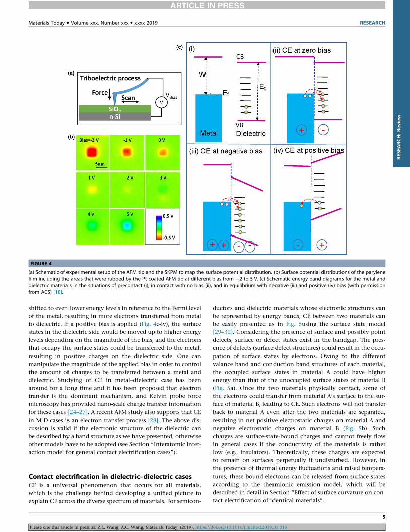
The sign of the charges to be delivered on a dielectric surfacecan be manipulated by applying a bias voltage on the metal tip(Fig. 4a, b) [20]. By tuning the applied bias on the metal tip from�5 V to +5 V, the charges delivered to the surface changed fromnegative to positive, and there was no charge exchange observedwhen the applied bias was 3 to 4 V. The mechanism of CE in M-Dcases can be well explained using an energy band diagram, inwhich the metal is characterized by its Fermi level, below whichall of the states are occupied and above which, all of the states areempty (assuming the temperature is 0 K). The dielectric surfacecan be characterized using its conduction band (CB) and valenceband (VB), but we must assume the presence of surface/defectsstates in the band gap due to the breaking of symmetry at the sur-face (Fig. 4c-i) [21]. If the edge of the valence band of the dielec-tric is below the Fermi level (Ef) of the metal, some of the surfacestates in the bandgap Eg with energy below Ef could be filled upby the electrons transferred from the metal into the dielectric,resulting in overall negative charges on the dielectric surface(Fig. 4c-ii) [22,23]. If a negative bias is applied on the metal tip(Fig. 4c-iii), the surface states on the dielectric side tend to be
3
oi.org/10.1016/j.mattod.2019.05.016

RESEA
RCH:R
eview
FIGURE 3
Comparison of electrostatic charge transfer dynamics between tapping mode and contact mode scans of an AFM tip. Surface potential mapping of parylenesample after the AFM probe scanned the central area at different scan speeds in (a) the tapping mode and (b) the contact mode. (c) and (d) Correspondingplots of surface potential change as functions of line scan time. (e) Comparison of the charge transfer density triggered by tapping mode and contact modeas a function of the tip–sample interaction time (with permission from Springer) [15].
FIGURE 2
(a) Schematic of experimental setup of the AFM tip and the SKPM to map surface potential distribution. (b) Triboelectric charge accumulation on the SiO2
surface with the increased counts of rubbing repetitions at the same area. Series of surface potential images taken in the same area from intact status to theone after the 8th rubbing cycle and (c) their corresponding potential profiles (With permission from ACS) [14].
RESEARCH Materials Today d Volume xxx, Number xx d xxxx 2019
4
Please cite this article in press as: Z.L. Wang, A.C. Wang, Materials Today, (2019), https://doi.org/10.1016/j.mattod.2019.05.016
RES
EARCH:Rev
iew
FIGURE 4
(a) Schematic of experimental setup of the AFM tip and the SKPM to map the surface potential distribution. (b) Surface potential distributions of the parylenefilm including the areas that were rubbed by the Pt-coated AFM tip at different bias from �2 to 5 V. (c) Schematic energy band diagrams for the metal anddielectric materials in the situations of precontact (i), in contact with no bias (ii), and in equilibrium with negative (iii) and positive (iv) bias (with permissionfrom ACS) [18].
Materials Today d Volume xxx, Number xxx d xxxx 2019 RESEARCH
shifted to even lower energy levels in reference to the Fermi levelof the metal, resulting in more electrons transferred from metalto dielectric. If a positive bias is applied (Fig. 4c-iv), the surfacestates in the dielectric side would be moved up to higher energylevels depending on the magnitude of the bias, and the electronsthat occupy the surface states could be transferred to the metal,resulting in positive charges on the dielectric side. One canmanipulate the magnitude of the applied bias in order to controlthe amount of charges to be transferred between a metal anddielectric. Studying of CE in metal–dielectric case has beenaround for a long time and it has been proposed that electrontransfer is the dominant mechanism, and Kelvin probe forcemicroscopy has provided nano-scale charge transfer informationfor these cases [24–27]. A recent AFM study also supports that CEin M-D cases is an electron transfer process [28]. The above dis-cussion is valid if the electronic structure of the dielectric canbe described by a band structure as we have presented, otherwiseother models have to be adopted (see Section “Interatomic inter-action model for general contact electrification cases”).
Contact electrification in dielectric–dielectric casesCE is a universal phenomenon that occurs for all materials,which is the challenge behind developing a unified picture toexplain CE across the diverse spectrum of materials. For semicon-
Please cite this article in press as: Z.L. Wang, A.C. Wang, Materials Today, (2019), https://d
ductors and dielectric materials whose electronic structures canbe represented by energy bands, CE between two materials canbe easily presented as in Fig. 5using the surface state model[29–32]. Considering the presence of surface and possibly pointdefects, surface or defect states exist in the bandgap. The pres-ence of defects (surface defect structures) could result in the occu-pation of surface states by electrons. Owing to the differentvalance band and conduction band structures of each material,the occupied surface states in material A could have higherenergy than that of the unoccupied surface states of material B(Fig. 5a). Once the two materials physically contact, some ofthe electrons could transfer from material A’s surface to the sur-face of material B, leading to CE. Such electrons will not transferback to material A even after the two materials are separated,resulting in net positive electrostatic charges on material A andnegative electrostatic charges on material B (Fig. 5b). Suchcharges are surface-state-bound charges and cannot freely flowin general cases if the conductivity of the materials is ratherlow (e.g., insulators). Theoretically, these charges are expectedto remain on surfaces perpetually if undisturbed. However, inthe presence of thermal energy fluctuations and raised tempera-tures, these bound electrons can be released from surface statesaccording to the thermionic emission model, which will bedescribed in detail in Section “Effect of surface curvature on con-tact electrification of identical materials”.
5
oi.org/10.1016/j.mattod.2019.05.016

RESEA
RCH:R
eview
FIGURE 5
Charge transfer (a) before contact, (b) in contact, and (c) after contact between two different insulator dielectrics for a case that En of the former is higher thanthat of the latter and the band structure model holds (with permission from Wiley) [17].
RESEARCH Materials Today d Volume xxx, Number xx d xxxx 2019
Interatomic interaction model for general contactelectrification casesThe discussions in Sections “Contact electrification in metal–dielectric cases” and “Contact electrification in dielectric–dielec-tric cases” are valid if the electronic structure of the dielectric canbe represented by a band diagram with the presence of surfaceand defect states. As for general materials, such as polymersand rubbers, their electronic structures can be represented bymolecular orbitals and chain alignment. An early review of obser-vations can be found in [33]. On the other hand, for materialsthat may not have a well characterized molecular structure orin the presence of composite phases, as in natural materials, suchas wool, wood, animal fur, and human hair, there is no simpleelectronic structure model that can represent these materials.We do know that all of these existing materials exhibit CE, andtherefore a general model is needed for explaining CE on atomicand molecular levels [16].
We first start from experimental observations. The first ques-tion is: how close must the two atoms be before CE occurs? Thisquestion was answered by our study using KPFM [34]. Fig. 6 pre-sents the surface potential difference (DV) between the center ofthe scanned area and the edge after a KPFM scan (Fig. 6a, c, e).Using amplitude-modulated (AM) AFM, the probe cantileverwas excited near its resonance frequency (f0), with a free vibra-tion amplitude (A0) set before the tip approaches the surface ofthe sample and a set-point scanning amplitude (Asp) set as a feed-back parameter to measure the topography of the sample surfaceafter engagement. The interaction of the tip with the surface willextend or delay its vibration phase shift (Du) if there is an attrac-tive or repulsive interaction between the two, respectively. Bycomparing the DV–Asp and Du–Asp curves of different A0 (100,70, and 50 nm), we explored the relationship between CE andthe change of phase shift in the tapping mode. For the experi-ments of A0 = 100 nm and A0 = 70 nm, there are dramaticincreases in DV from 0 (which means that contact electrificationhas had a significant influence on the surface potential) with Asp
being smaller than certain values (�95 nm for the experiment ofA0 = 100 and 62.5 nm for the experiment of A0 = 70 nm), and
6
Please cite this article in press as: Z.L. Wang, A.C. Wang, Materials Today, (2019), https://d
these values correspond to the sign switch point of the Du inthe Du–Asp curves. In the case of A0 = 50 nm, no CE wasobserved. Also, there is no decrease in the phase shift under suchcircumstances. When the tip has a net attractive force, it is in theattractive regime, and there is an increase in the phase shift(Du > 0). In contrast, if it has net repulsive force, it will be inthe repulsive force regime, and there will be a decrease fromthe original phase shift (Du < 0). Therefore, the sign of Du couldbe regarded as the symbol of the net tip–sample interaction forcefor each vibration cycle.
Accordingly, if the tip is in the attractive regime (A0 = 50 nm),there is no electron transfer between the tip and sample. Byincreasing the free amplitudes (A0 = 70 and 100 nm), the probecantilever can vibrate with more energy. In this way, it couldovercome the repulsive force and enter into the repulsive region.In this case, the tip is much closer to the surface of the sample inits lowest possible position (as shown in Fig. 6d, e). Since this tip–sample distance could result in tunneling, CE is observed in scan-ning experiments with A0 = 100 and 70 nm (Fig. 6g). Moreover,since the Asp for the transition between the attractive regimeand the repulsive force regime is exactly the same value for thedrastic increase in DV from 0 (�95 nm for the experiment ofA0 = 100 and 62.5 nm for A0 = 70 nm), the distance between thetip and the sample for electron transfer to occur should be smaller thanthe interatomic distance at equilibrium, where the long range attrac-tive force equals to the short-range repulsive force.
The repulsive and attraction interactions between atoms canbe easily understood from the interatomic interaction potential.Fig. 7a shows the general representation of interatomic interac-tions. For two atoms that form a bond, which means some sortof overlap in electron clouds or wave function, an equilibriumdistance a is established, which is called the bond length or inter-atomic distance. If the interatomic distance x is shorter than a,the two atoms tend to repel each other owing to the increasedoverlap of electron clouds (Fig. 7b). One of the key factors inCE is an external force that has to be applied in order for thetwo surfaces to be contacted. The role played by such an exter-nally applied force is to create local high pressure at certain
oi.org/10.1016/j.mattod.2019.05.016

RES
EARCH:Rev
iew
FIGURE 6
Exploring the relationship between contact electrification and the phase shift of the AFM cantilever in order to probe the force zone within which chargetransfer occurs. (a–f) Surface potential difference DV–Asp and Du–Asp curves under the conditions of A0 = 100, 70, and 50 nm. (g) Schematic of the tip-sampleinteraction force of tapping scans with different scanning parameters (A0 and Asp), as defined in (g). Whether the tip is in the attractive regime or repulsiveregime above the surface of the sample can be deduced from the change of the phase shift (Du) during the tapping vibration (with permission from ACS)[18].
FIGURE 7
Interatomic interaction potential between two atoms and the force between the two when they are (a) at equilibrium position, (b) with strong electron cloud/wave-function overlap in the repulsive region, and (c) with little electron cloud/wave-function overlap in the attractive region.
Materials Today d Volume xxx, Number xxx d xxxx 2019 RESEARCH
7
Please cite this article in press as: Z.L. Wang, A.C. Wang, Materials Today, (2019), https://doi.org/10.1016/j.mattod.2019.05.016

RESEA
RCH:R
eview
RESEARCH Materials Today d Volume xxx, Number xx d xxxx 2019
contacting points even at atomic and nano-scales, where theinteratomic distance x is forced to be shorter than a betweenthe local contacting points, resulting in local repulsive force. Ifthe interatomic distance x is larger than a, the two atoms tendto attract each other due to the reduced overlap of electronclouds, nearly breaking their bond (Fig. 7c).
The experimental results in Fig. 6 indicate that the distancebetween the AFM tip and the silica surface has to be shorterthan the bonding length in order for the two to experienceCE. In the repulsive region, the increased overlap in local elec-tron clouds results in electron transition from one material tothe other. Therefore, we can propose an atomic-scale chargetransfer mechanism for CE [16,35]. Fig. 8a shows a case inwhich, prior to the atomic-scale contact of the two materials,their respective electron clouds remain separated without over-lap. This is the attractive force region as presented in Fig. 8. Thepotential well binds the electrons tightly in specific orbitals andstops them from freely escaping, which is the case for non-conducting materials. When the two atoms belonging to twomaterials, respectively, get close to and contact with each other,
FIGURE 8
An electron-cloud-potential-well model proposed for explaining CE and charge tenergy band structure, for general material cases. Schematic of the electron clomaterials A and B, respectively, when they are: (a) before contact, (b) in contact,after being forced to have electron cloud overlap. (d) Charge release from the adistance between two nuclei; EA and EB, occupied energy levels of electrons; E1 aof (b) to show that the increased electron cloud overlap results in a lower potentiand possible photon emission (with permission from Wiley) [17].
8
Please cite this article in press as: Z.L. Wang, A.C. Wang, Materials Today, (2019), https://d
the electron clouds overlap between the two atoms to form anionic or covalent bond. The bonding lengths are shortenedeven more if an external compression force is applied. In thiscase, the initial single potential wells become an asymmetricdouble-well potential, and the energy barrier between the twois lowered as a result of strong electron cloud overlap(Fig. 8b). Then electrons can then transfer from one atom tothe other, resulting in CE. The role played by mechanical con-tact of the two materials is to shorten the distance between theatoms and cause a strong overlap of their electron clouds in therepulsive region, at least in the area at which the atomic-scalecontact occurs, despite the samples being larger. It is importantto note that only a very small fraction of area of the two sur-faces will reach atomic scale contact. This also explains whymore charges are transferred if one material rubs against theother harder/tighter owing to the strong compression forceapplied in sliding process, which can even cause local fracturesand plastic deformation. After being separated (Fig. 8c), thetransferred electrons remain as static charges on the material’ssurface.
ransfer and release between two materials that may not have well-specifiedud and potential energy profile (3D and 2D) of two atoms belonging to twoand (c) after contact, showing electron transfer from one atom to the othertom at an elevated temperature T once kT approaches the barrier height. d,nd E2, potential energies for electrons to escape. (b1–b3) Detailed illustrational barrier between the two atoms, resulting in interatomic electron transition
oi.org/10.1016/j.mattod.2019.05.016
Materials Today d Volume xxx, Number xxx d xxxx 2019 RESEARCH
The model proposed in Fig. 8 is also supported by quantummechanical calculations, which state that the driving force forelectrons to transfer is due to the delocalization of electron wavefunctions due to contact and strain [16,36–39], which is what werefer to as the state of strong overlap of electron clouds understress. It is in this range that electron transfer is possible. Thetransition probability of an electron from one atom to the otheras a function of the interatomic distance has been calculated[40], and the results support our discussion presented in Fig. 8.
RES
EARCH:Rev
iew
Photon emission in contact electrificationBased on our model presented in Fig. 8, several photon emissionprocesses are proposed [18]. According to Fig. 8b1–b3, energyreleased by electron transfer from dielectric A to dielectric Bcan be in the form of photon emission, plasmon excitation,and/or phonon excitation. Photon emission, if possible, can beused for studying the transition from the surface states of dielec-tric A to the surface states of dielectric B. The emitted photonshould have energy in tens of eV, possibly resulting in UV, visiblelight, microwave, and even THz wave emission when two mate-rials contact. The above proposed processes, if potentially observ-able as light emission, could give birth to a new opticalspectroscopy for studying electronic transitions at interfaces.These results remain to be verified experimentally.
The energy of CE-produced electrons is not expected toexceed tens to hundreds of eV. By bombarding a metal plateusing electrons emitted during peeling a piece of tape in vacuum,continuous X-rays with energies centered around 15 keV havebeen observed [41]. Considering the high electric field generatedby CE charges, in the order of 105–106 V/m according to an AFMstudy [17], it is possible to generate a high voltage. Freely releasedelectrons accelerated by such high voltages could result in strongX-ray radiation [42]. More study is needed in order to understandthe observed phenomenon.
Effect of surface curvature on contact electrification ofidentical materialsIt is generally known that physical contact of two dissimilarmaterials produces electrostatic charges, but experiments haveshown that contact between two identical insulators also pro-duces static charges [43–47]. In particulate materials, such assand, smaller particles tend to be negatively charged and largerparticles of the same material tend to be positively charged[48–50]. Such observations cannot be explained using either ofthe models we have proposed for dissimilar materials.
In order to understand the underlying mechanism in suchcases, we have carried out detailed studies of the CE of two piecesof chemically identical materials that possess different curva-tures, such as PTFE, Kapton, FEP, polyester, and nylon [51]. Poly-mers are chosen because we can change their curvature easily. Byrationally designing materials with different surface curvatures,our results indicate that CE of two pieces of chemically identicalmaterials results in concave surfaces being positively charged andconvex surfaces being negatively charged (Fig. 9a–c). Our inter-pretation is that, owing to the fact that surfaces with differentcurvatures would have different surface energies possibly dueto the stretched or compressed surface molecules, the energies
Please cite this article in press as: Z.L. Wang, A.C. Wang, Materials Today, (2019), https://d
for specific surface states of the materials would be shifted con-sidering the effects from surface energy (Fig. 9d). As a result, anelectron can transfer from one material surface to another chem-ically identical surface with shifted surface states, once theyphysically contact (Fig. 9e). Furthermore, this means that thepresence of a curved surface “breaks” the symmetry of the twosides, thus shifting the energy levels of surface states, resultingin electron transition, albeit with a smaller probability than dis-similar materials. The correlation of altered surface curvaturewith changes in surface energy is also supported by a theoreticalstudy [52]. With considering a variation on surface morphologyat the nano level and a rise of local temperature during probescanning, mosaic surface charge distribution has been observedon surfaces [53].
Effect of temperature on contact electrificationIn all of the existing literatures on triboelectrification, few studiesare available about the temperature dependence of CE, as almostall of the measurements were made at room temperature. Thislack of temperature dependence studies is potentially the basisof the confusion over whether charge transfer is due to electrons,ions or even materials species. We have recently studied the tem-perature dependence of CE, and our main conclusion is that elec-tron transfer is the dominant, if not exclusive, mechanism forCE.
Transfer of charges across an interfaceThe temperature dependence of CE has been directly proved byscanning an Au tip on a SiO2 surface (Fig. 10a) [54]. It is possiblethat the electrons would be thermally excited and transferredfrom the hotter material side to the cooler side. Hence, thecharge transfer between the tip and the sample may be manipu-lated by setting the tip and sample to different temperatures. Toverify this, the sample temperature was controlled at 373 K,while the SiO2 sample temperature was varied from 313 K to403 K. As shown in Fig. 10b, the transferred charge densityincreased linearly with rising tip temperature. When the tip tem-perature increased, the electrons in the tip were excited and moreprone to hopping from the tip to the SiO2 sample, and the sam-ple became more negatively charged after contact.
The observed result can be explained using an energy banddiagram, as shown in Fig. 10c [31]. Since the experiment wasdone at a temperature higher than 0 K, the distribution of elec-trons in the metal at different energies follows the Fermi–Diracfunction:
f Eð Þ ¼ 1
e ðE�Ef Þ=kTð Þ þ 1ð1Þ
where f Eð Þ denotes the probability of an electron in the energy level E,Ef denotes the Fermi level of the metal. Above the Fermi level, there isa tail filled with electrons.
In the first case, we assume that the Fermi level (Ef ) of themetal is higher than the highest occupied surface state level(E0) of the dielectric, and the metal tip temperature (Tm) is lowerthan the dielectric temperature (Td) (Tm < Td) (Fig. 10c-i), hencethe energy increase in electrons in the metal (�kTm) will be lowerthan the increase in electron energy in the dielectric (�kTd). Inthis case, the electrons transfer from the metal to the dielectric
9
oi.org/10.1016/j.mattod.2019.05.016

RESEA
RCH:R
eview
FIGURE 9
Mechanism of CE between identical polymer materials of different surface curvatures. (a–c) Charge transfer before contact, in contact, and after contactbetween identical material surfaces A and B with different surface curvatures, and (d–f) corresponding explanation of the surface charge transfer by thesurface states model. LUMO, lowest unoccupied molecular orbital; En, neutral level of surface states; HOMO, highest occupied molecular orbital (withpermission from ACS) [30].
RESEARCH Materials Today d Volume xxx, Number xx d xxxx 2019
in CE, as shown in Fig. 10c-ii. If the dielectric temperature isdecreased while the metal temperature remains unchanged(Tm ¼ Td), as shown in Fig. 10c-iii, the energy increase in elec-trons in the metal (�kTm) will be equal to the increase in electronenergy in the dielectric (�kTd). This leads to more electrons hop-ping from the metal to the dielectric than in the situation whenTm < Td, as shown in Fig. 10c-iv. If the metal temperature isincreased while the dielectric temperature remains unchanged(Tm > Td), as shown in Fig. 11c-v, the increase in electron energyin the metal (�kTm) will be higher than the increase in electronenergy in the dielectric (�kTd). This leads to more electrons hop-ping from the metal to the dielectric, as shown in Fig. 10c-vi.Since the dielectric temperature remains unchanged, the amountof electron tunneling back to the metal during surface separationremains nearly unchanged. Therefore, the triboelectric chargeson the dielectric surface increase in this case.
The trend of CE is very muchmaterial dependent. By scanningan Au tip on aluminum nitride (AlN), the transferred charge den-sity on the AlN surface was almost zero when the tip temperaturewas equal to the sample temperature (Fig. 11a). However, the AlNgainedmorenegative charges from scanningwhen the tip temper-ature was higher than the sample temperature. The CE on Si3N4
experienced a sign reversal with an increase in tip temperature(Fig. 11b). The results show that, no matter if the transferredcharges are positive or negative, more electrons are injected intothe sample when the tip temperature is increased than when the
10
Please cite this article in press as: Z.L. Wang, A.C. Wang, Materials Today, (2019), https://d
tip temperature equals the sample temperature. This is consistentwith the thermionic electron emission model, in which the elec-trons in the tip are excited when the tip temperature increasesand aremore likely to transfer to the sample,making the triboelec-tric charges on the sample surface more negative.
In the second case, the Fermi level of the metal is lower thanthe highest occupied surface state level of the dielectric, andTm ¼ Td, as shown in Fig. 11c-i. The electrons will transfer fromthe dielectric to the metal, and the dielectric will be positivelycharged, as shown in Fig. 11c-ii. When the metal temperatureis increased, and the dielectric temperature remains unchanged(Tm > Td), as shown in Fig. 11c-iii, the energy increase in elec-trons in the metal will be higher than the increase in electronenergy in the dielectric. The gap between the effective Fermi levelof the metal and the highest occupied surface state level of thedielectric becomes smaller, which leads to less electron hoppingfrom the dielectric to the metal, and the dielectric receives fewerpositive charges in CE, as shown in Fig. 11c-iv. In particular, ifthe metal temperature continues to increase and the dielectrictemperature remains unchanged (Tm � Td), the effective Fermilevel of the metal will be higher than the highest occupied sur-face state level of the dielectric, as shown in Fig. 11c-v. In thiscase, the electrons will transfer from the metal to the dielectric,and the polarity of the transferred charges in the CE will bereversed (Fig. 11c-vi), as observed in the CE between the Au-coated tip and Si3N4.
oi.org/10.1016/j.mattod.2019.05.016

RES
EARCH:Rev
iew
FIGURE 10
Proving the effect of temperature differences on CE between the Au-coated tip and the SiO2 sample by KPFM at nano-scale. (a, b) The sample temperaturewas set at 373 K, while the tip temperature varied from 313 K to 433 K. (c) The band structure model of the temperature difference induced charge transfer(Ef > E0). The band structure of the metal and surface states of the dielectric, when (i) the metal temperature is lower than the dielectric temperature, (iii)the metal temperature equals to the dielectric temperature, and (vi) the metal temperature is higher than the dielectric temperature. The illustration ofcontact charge transfer between the metal and the dielectric, when (ii) the metal temperature is lower than the dielectric temperature, (iv) the metaltemperature equals to the dielectric temperature, and (v) the metal temperature is higher than the dielectric temperature (With permission from Wiley) [32].
Materials Today d Volume xxx, Number xxx d xxxx 2019 RESEARCH
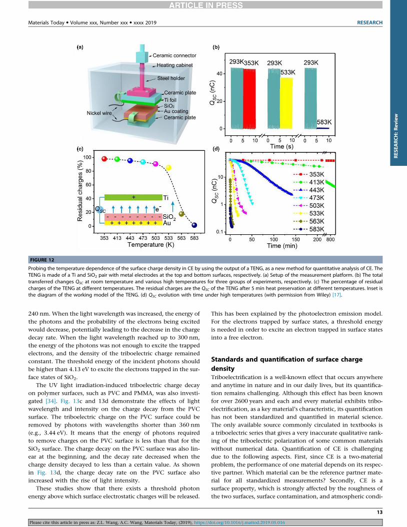
Release of surface electrostatic chargesThe TENG operates by coupling triboelectrification with electro-static induction. The triboelectric field produces a driving forcethat makes electrons in the top and bottom metal electrodesflow due to the electrostatic induction effect. The measuredtotal charges QSC flowing under the short circuit condition isa direct measure of the surface charge density, providing anew methodology for proving triboelectrification. Our TENGstudy has unearthed a surprising result: triboelectrification dis-appears at high temperature [16,18]. A TENG was constructedfrom thermally stable materials, such as Ti and SiO2, as shownin Fig. 12a, so that the operating temperature could be uni-formly increased. Fig. 12b shows the change of total outputcharges QSC of the TENG at temperatures of 353 K, 533 K and583 K, demonstrating that the charge density decreased more
Please cite this article in press as: Z.L. Wang, A.C. Wang, Materials Today, (2019), https://d
rapidly at higher temperatures. When the temperature reached583 K, the charges quickly disappeared and the total QSC wasless than 1 nC, similar to the disappearance of magnetismabove the Curie temperature. Fig. 12c shows the residualcharges on the TENG after 5 min of measurement at differenttemperatures, and the inset is the diagram of the Ti-SiO2 TENG.The residual charges decreased more rapidly with the increasein temperature, and it is interesting to note that they startedto decrease more rapidly once the temperature was higher than533 K. Fig. 12d shows long-term charge decay under high tem-peratures, which indicates that increased temperatures lead tocharge decay.
By quantitatively comparing the charge dissipation curve as afunction of temperature, we concluded that the release ofcharges is best described by the thermionic electron emission
11
oi.org/10.1016/j.mattod.2019.05.016

RESEA
RCH:R
eview
FIGURE 11
Proving the effect of temperature difference on the CE between an Au-coated tip and AlN and Si3N4 sample by KPFM at nano-scale. The relationship betweentransferred charge density on the (a) AlN, and (b) Si3N4 surfaces and the tip temperature when the sample temperature is maintained at 313 K. (c) The band-structure model of the temperature-difference induced charge transfer (Ef < E0). (i, iii, v) The band structure of the metal and surface states of the dielectric,when the metal temperature equals the dielectric temperature, the metal temperature is higher than the dielectric temperature, and the metal temperatureis much higher than the dielectric temperature, respectively. (ii, iv, vi) Illustrations of the contact charge transfer between the metal and the dielectric, whenthe metal temperature equals the dielectric temperature, the metal temperature is higher than the dielectric temperature, and the metal temperature ismuch higher than the dielectric temperature (With permission from Wiley) [32].
RESEARCH Materials Today d Volume xxx, Number xx d xxxx 2019
model, and the measured QSC values may be fitted according tothe thermionic emission equation [55,56]:
J ¼ kA0T2e
�WkT e
DWkT � 1
h ið2Þ
where J is the current density, k is the material-specific correction fac-tor, A0 is Richardson’s constant of a free electron, T is temperature, Wis the height of the potential barrier, k is Boltzmann’s constant andDW is the potential barrier height variation due to the surface electricfield E. When DW << kT, the emission current density is related to thetotal transferred charges in a TENG by [16]
J � k1A0
kTe
�WkT QSC ð3Þ
or equivalently:
lnJ
A0T
� �¼ �W
kTþ ln
k1kQSC
� �ð4Þ
Data simulation using Eq. (4) fits the experimental data well.Therefore, the dissipation of the charges on the surface followsthe electron thermionic emission model.
Effect of photon excitation on contact electrificationSurface electrostatic charges can be released under photon excita-tion [57]. This process has been investigated by illuminating aninsulator surface with light at a specific wavelength and inten-
12
Please cite this article in press as: Z.L. Wang, A.C. Wang, Materials Today, (2019), https://d
sity. A requirement is to maintain that there is no significantchange in surface temperature during the KPFM measurement,so that temperature effects can be ruled out. As shown inFig. 13a, the triboelectric charges on the insulator surface weregenerated using the peakforce tapping mode, in which the tipcontacts the insulator surface in a point by point “dancing”mode. After the CE, the triboelectric charge density on the insu-lator surface was measured using the KPFM mode. Furthermore,the charged area on the insulator surface was irradiated by UVlight, and the triboelectric charge density remaining on the sur-face was measured at regular time intervals to record the chargedecay.
In order to further verify the photoelectron emission of elec-trons in CE, the effects of light wavelength and intensity onthe irradiation induced triboelectric charge decay were studied.Fig. 13b shows the effect of the incident light wavelength onthe decay of triboelectric charges from the SiO2 surface [34].The charge decay rate was fastest when the wavelength was240 nm, and the decay rate decreased with the increase in wave-length. In particular, the amount of the triboelectric chargesremained constant when the wavelength rose up to 300 nm.The probability of the electrons, which were trapped in surfacestates following CE, being excited out of the surface was the lar-gest under the irradiation of the light with a wavelength of
oi.org/10.1016/j.mattod.2019.05.016
RES
EARCH:Rev
iew
FIGURE 12
Probing the temperature dependence of the surface charge density in CE by using the output of a TENG, as a new method for quantitative analysis of CE. TheTENG is made of a Ti and SiO2 pair with metal electrodes at the top and bottom surfaces, respectively. (a) Setup of the measurement platform. (b) The totaltransferred changes QSC at room temperature and various high temperatures for three groups of experiments, respectively. (c) The percentage of residualcharges of the TENG at different temperatures. The residual charges are the QSC of the TENG after 5 min heat preservation at different temperatures. Inset isthe diagram of the working model of the TENG. (d) QSC evolution with time under high temperatures (with permission from Wiley) [17].
Materials Today d Volume xxx, Number xxx d xxxx 2019 RESEARCH
240 nm. When the light wavelength was increased, the energy ofthe photons and the probability of the electrons being excitedwould decrease, potentially leading to the decrease in the chargedecay rate. When the light wavelength reached up to 300 nm,the energy of the photons was not enough to excite the trappedelectrons, and the density of the triboelectric charge remainedconstant. The threshold energy of the incident photons shouldbe higher than 4.13 eV to excite the electrons trapped in the sur-face states of SiO2.
The UV light irradiation-induced triboelectric charge decayon polymer surfaces, such as PVC and PMMA, was also investi-gated [34]. Fig. 13c and 13d demonstrate the effects of lightwavelength and intensity on the charge decay from the PVCsurface. The triboelectric charge on the PVC surface could beremoved by photons with wavelengths shorter than 360 nm(e.g., 3.44 eV). It means that the energy of photons requiredto remove charges on the PVC surface is less than that for theSiO2 surface. The charge decay on the PVC surface was also lin-ear at the beginning, and the decay rate decreased when thecharge density decayed to less than a certain value. As shownin Fig. 13d, the charge decay rate on the PVC surface alsoincreased with the rise of light intensity.
These studies show that there exists a threshold photonenergy above which surface electrostatic charges will be released.
Please cite this article in press as: Z.L. Wang, A.C. Wang, Materials Today, (2019), https://d
This has been explained by the photoelectron emission model.For the electrons trapped by surface states, a threshold energyis needed in order to excite an electron trapped in surface statesinto a free electron.
Standards and quantification of surface chargedensityTriboelectrification is a well-known effect that occurs anywhereand anytime in nature and in our daily lives, but its quantifica-tion remains challenging. Although this effect has been knownfor over 2600 years and each and every material exhibits tribo-electrification, as a key material’s characteristic, its quantificationhas not been standardized and quantified in material science.The only available source commonly circulated in textbooks isa triboelectric series that gives a very inaccurate qualitative rank-ing of the triboelectric polarization of some common materialswithout numerical data. Quantification of CE is challengingdue to the following aspects. First, since CE is a two-materialproblem, the performance of one material depends on its respec-tive partner. Which material can be the reference partner mate-rial for all standardized measurements? Secondly, CE is asurface property, which is strongly affected by the roughness ofthe two surfaces, surface contamination, and atmospheric condi-
13
oi.org/10.1016/j.mattod.2019.05.016

RESEA
RCH:R
eview
FIGURE 13
Probing the effect of photon excitation on the CE between an Au-coated tip and SiO2 sample by KPFM at nano-scale. (a) Schematic illustration of the AFM andUV light irradiation experiments. (b) The effects of light wavelength on the charge decay on SiO2 surface. The effects of (c) the light wavelength and (d) thelight intensity on the charge decay on the PVC surface. In all of the experiments, careful measurements were made to ensure there was no significant increasein the sample temperature during the measurements (with permission from Wiley) [57].
RESEARCH Materials Today d Volume xxx, Number xx d xxxx 2019
tions, as well as humidity. A standardized method must be estab-lished to uniformly measure all of the materials, if possible.
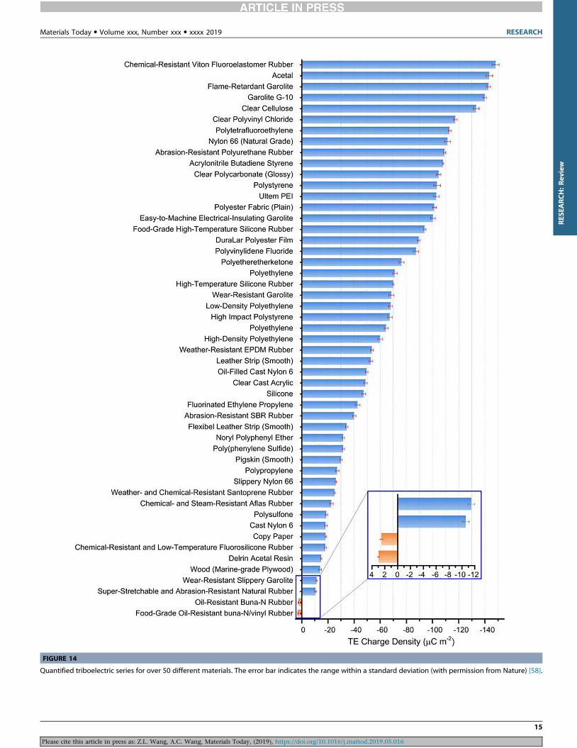
We recently introduced a universal standard method to quan-tify the triboelectric series for a wide range of polymers, establish-ing a fundamental materials property of quantitativetriboelectrification [58]. To maximize the contact of a materialwith the reference material, we chose liquid metal as the countercontact, which is likely to have the maximum atomic-scale con-tact, shape adaptability and softness. This method standardizesthe experimental setup for uniformly quantifying the surface tri-boelectrification of general materials. The normalized triboelec-tric charge density (TECD) was defined and derived to revealthe intrinsic tendency of polymers to gain or lose electrons. Atable is given regarding the TECD of over 50 materials (Fig. 14).This first quantitative triboelectric series will be a textbook stan-dard for implementing the application of triboelectrification forenergy harvesting and self-powered sensing. The methodologyestablished will be extended to all conventional materials, suchas ceramics, semiconductors, and polymers.
Discussion and summaryElectron transfer versus ion transfer in contact electrificationIt has been long debated over whether CE is due to electrontransfer, ion transfer, or even materials species transfer. First-principles’ simulations [59] on surfaces of alumina and silica sup-
14
Please cite this article in press as: Z.L. Wang, A.C. Wang, Materials Today, (2019), https://d
port the role of adsorbed water in surface charging: OH� may bea dominant charge-carrying ion, through both surface trans-ports, adsorption and desorption. OH� ions are believed to accu-mulate at interfaces [60]. Studying CE at various elevatedtemperatures and photon excitations have clearly ruled out thecontribution made by ion transfer, especially in solid–solid cases[17,37]. Firstly, the mechanism of releasing surface charges fol-lows the electron thermionic emission model. Ion transfer satis-fies the Boltzmann distribution [12], which indicates that moretriboelectric charges would be transferred at higher temperatures,and this evidently disagrees with our experimental observations.Secondly, water plays a very important role in the ion transfermodel [61], but fewer charges are transferred at higher moisturelevels and maximum charge transfer has been found to occurat �0% relative humidity [62]. A recent study carried out tribo-electric charging in oil, and showed that water is not necessaryfor contact electrification to occur [63]. Thirdly, CE between Tiand SiO2 was observed even at 623 K, at which there are hardlyany water-related ions remaining on solid surfaces [18]. Fourthly,studies by Wang et al. indicated that CE at a vacuum of 10�6 Torrwas five times higher than that at one atmosphere pressure [64].There are hardly any water molecules adsorbed on solid surfacesat such a high vacuum in comparison to ambient cases. Lastly,Liu et al. showed that a sustainable tunneling current had beenproduced using an unbiased, triboelectrically charged metal–insulator–semiconductor (MIS) point contact system [65]. All of these
oi.org/10.1016/j.mattod.2019.05.016
RES
EARCH:Rev
iew
FIGURE 14
Quantified triboelectric series for over 50 different materials. The error bar indicates the range within a standard deviation (with permission from Nature) [58].
Materials Today d Volume xxx, Number xxx d xxxx 2019 RESEARCH
15
Please cite this article in press as: Z.L. Wang, A.C. Wang, Materials Today, (2019), https://doi.org/10.1016/j.mattod.2019.05.016
RESEA
RCH:R
eview
RESEARCH Materials Today d Volume xxx, Number xx d xxxx 2019
phenomena indicate that water ions are not necessary for CE,and the CE has to be an electron-dominated transition process.
Based on our studies, our conclusion is that CE is largely if notexclusively due to electron transfer. Electron transfer occurs if theinteratomic distance is in the range of the repulsive force region,within which the electron clouds have maximized overlap. Sur-face discharge at elevated temperatures follows the electron ther-mionic emission model. The sign of the transferred charges in CEcan be reversed by applying an electric field. Further studiesfound that the work required to separate the charged surfaceswas comparable to the fracture energies of materials, whichrevealed that the electrification was associated with the interac-tions in electron clouds [66]. These studies indicate that the elec-trification is strongly related to electron transfer during theoverlap of electron clouds, which further rule out the ion transfermechanism. Finally, any contact between surfaces typicallyinvolves making and breaking of bonds, and CE is a consequenceof such a process. Therefore, understanding of CE at the atomic-and nano-scale is fundamentally important for understandingbond formation and breaking between atoms.
A typical surface charge density related to triboelectrificationcan measure up to �10�3 C/m2 in ambient condition, which cor-responds to �8 excess electrons per 10000 nm2 of surface area.Thus, the probability of electron transfer is about one out of30,000 surface atoms. Although this chance appears rather small,this charge transfer is an important quantummechanical processthat occurs in our lives at any place and any time.
Contact electrification at liquid–solid interfaces and theformation of EDLCE occurs not only for solid–solid pairs but also at the interfacesbetween solids, liquids and gases, such as a raindrop with air inthe liquid–gas case, sand particles with air in the solid–gas case,and at the solid–solution interface. A well-known phenomenonis the formation of an electrical double layer (EDL) at solid–liquidinterfaces, which appears on the surface of an object when it isexposed to a liquid. The object might be a solid particle, a gasbubble, or a liquid droplet. The EDL refers to two parallel layersof charges surrounding the object. The first layer, the surfacecharge (either positive or negative), consists of ions adsorbedonto the object due to chemical interactions. The second layeris composed of ions attracted to the surface charges via the Cou-lomb force from the solution, electrically screening the first layer.This second layer is made of free ions that move in the liquidunder the influence of electric attraction and thermal motionrather than being firmly anchored. Although the existence ofEDL is a fact and its structure is clear, a fundamental questionwe would seek to ask is, what is the cause of the first layer becom-ing charged at the very beginning when it first contacts with aliquid? It might be related to the electron dominated CE at a veryearly stage of the object being exposed to a solution, as presentedbelow.
The formation of the EDL is proposed as a two-step process. Inthe first step, when the molecules in the solution first approach avirgin surface that has no pre-existing surface charges (Fig. 15a),it may be possible that the atoms/molecules in the solutiondirectly interact with the atoms on the solid surface to formstrong overlap of electron clouds, as shown in Figs. 7 and 8. Elec-
16
Please cite this article in press as: Z.L. Wang, A.C. Wang, Materials Today, (2019), https://d
tron transfer occurs first to make the “neutral” atoms on solidsurface become charged, i.e., the formation of ions (Fig. 15b).For easy illustration, we label eight molecules as A–H, so onecan easily follow the movements of the specific molecules at dif-ferent stages. Under the pressure of the liquid flow or turbulence,the liquid molecules that are adjacent to the solid surface arethus forced/pushed off of the interface region by breaking theformed “bonds”, leaving a layer of ions affixed to the solid sur-face (Fig. 15c) with the severed molecules becoming freelymigrating ions in the liquid. It must be pointed out that the den-sity of such surface charges should be comparable to the surfacecharge density in CE (�one out of 30,000 surface atoms, verysparsely distributed on the surface rather than the denselypacked layers as depicted in many textbooks). In the second step,if there are ions existing in the liquid, such as H+ and OH�, theloosely distributed negative ions in the solution would beattracted to migrate toward the surface bonded ions due to elec-trostatic interactions, forming an EDL. The f potential is intro-duced to characterize the EDL. Our suggestion here is that theorigin of forming the EDL is likely the result of CE due to electrontransfer at the very first step. Once the EDL is formed, many dis-cussions and models in the literatures regarding related potentialdistribution and surface chemistry are appropriate.
Contact electrification at liquid–gas and liquid–liquidinterfacesThe model presented in Figs. 7 and 8 can also be applied toexplain the CE between gas and a liquid. A well-known case isthe friction between air molecules with water droplets to makecharged raindrops. The water droplet is negatively charged dueto the electron transfer from air molecules to the water dropletwhen the molecules strike the liquid surface. The charged mole-cules in a water droplet are loosely bound and free to move, andthe charged air molecules tend to fly off the surface due to blow-ing of air and bombardment by other molecules. Thus, the totalraindrop is negatively charged once it precipitates and fallsthrough air.
By the same token, CE between liquid–liquid pairs should alsoexist. By compressing the molecules of one type of liquid againstthe surface of another liquid, the interface between the two isexpected to be charged if they are immiscible, as a result of elec-tron transfer. However, studies of this line of research are few.
Contact electrification at the interface of p- and n-typesemiconductorsCE as for conventional materials can also occur for p- and n-semiconductors. Since the width of the depletion region at apn junction is typically around a few nm, but CE occurs onlyat the top one to two atomic layers. The surface states at the n-side are filled with electrons, and the surface states are occupiedby holes. At the very interface, in reference to Fig. 5 for insula-tors, a transition of electrons from the surface states of n-sideto the hole states at p-side is likely to occur, resulting in p sideto be negatively charged due to CE, and n-side positivelycharged. The energy released by such a transition could exciteelectron-hole pairs at the pn interface, possibly resulting in anobservable current flowing from p-side to the n-side in the
oi.org/10.1016/j.mattod.2019.05.016

RES
EARCH:Rev
iew
FIGURE 15
A proposed two-step model on the procedures for forming an electric double layer at a liquid–solid interface. The first step: formation of the very first layer ofelectrostatic charges on the solid surface. (a) Schematic representation of molecules in solution; (b) the adsorption of molecules on the surface and electrontransfer, resulting in the surface being charged; and (c) the adsorbed molecules being pushed off the adsorbed locations due to the pressure of the liquid.The second step: segregation of ions in the liquid: (d) the presence of the charged surface as a result of the first step and (e) adsorption of ions in liquid oncharged solid surface, forming the EDL.
Materials Today d Volume xxx, Number xxx d xxxx 2019 RESEARCH
external circuit, similar to photovoltaic effect. This may be sim-ply referred to as the tribovoltaic effect.
By contacting a piece of p-type Si and an n-type Si wafer, annon-symmetric AC current has been observed in the external cir-cuit [67], with a large current observed when the two pieces areseparated apart and a smaller current is received when the twopieces are contacted with each other. This observed AC signalwas interpreted as a result of difference in chemical potential asa result of redistribution of electric carriers. Here, we suggest thatthe current flowing from n-side to p-side when the n and p semi-conductors are separated apart is likely due to carrier redistribu-tion as suggested by Zhang et al., and the current flowing fromp-side to n-side when the n and p semiconductors are contactedis possibly due to the tribovoltaic effect as discussed above,because CE is unavoidable when two materials are contacted.There are only limited studies available on the CE at a pnjunction.
Alternatively, by sliding a n-semiconductor on top of a p-semiconductor without changing the current area (so calleddynamic pn junction), the DC current observed by Lin et al.[68] is likely due to the tribovoltaic effect proposed above. Exten-sively studies are being carried out to verify the detailed mecha-nism of CE for semiconductor systems.
Advances in fundamental sciences and perspectivesWe believe that we have answered the following fundamentalquestions related to electricity:
(1) How are the electrostatic charges being created?This question is answered by the contents reviewed in thispaper about CE, which should provide a fundamental
Please cite this article in press as: Z.L. Wang, A.C. Wang, Materials Today, (2019), https://d
understanding about how the electrostatic charges are cre-ated. We hope that an open question for over 2600 yearshas been answered.
(2) How do the electrostatic charges drive electrons to flow?One way of outputting power using electrostatic charges isthe TENG, which is governed by the Maxwell displacementcurrent covered elsewhere [69,70]. The displacement cur-rent is created by coupling CE and electrostatic induction,so that electrons in metal electrodes are driven to flowunder the mechanical triggering. This is the process ofhow the electric power is generated due to electrostaticinteraction.
(3) How is the surface charge density quantified and cali-brated?This is answered in Section “Standards and quantificationof surface charge density”.
(4) How is the current used for technologies?This is the basic technological application of TENG infields like health care, environmental science, wearableelectronics, internet of things, robotics, and artificial intel-ligence. Comprehensive review on TENG can be foundelsewhere [9–11].
In summary, although CE has been known for 2600 years,longer than any recorded effect in science, its understandingremains premature. This paper reviews the updated progress instudying the fundamental mechanism of CE. Our main conclu-sion is that electron transfer is the dominant, if not exclusive,mechanism for CE. Ion transfer is a result of electron transferat the very beginning, such as in the formation of the EDL atsolid–liquid interfaces. Electron transfer due to overlapped
17
oi.org/10.1016/j.mattod.2019.05.016

RESEA
RCH:R
eview
RESEARCH Materials Today d Volume xxx, Number xx d xxxx 2019
electron clouds under mechanical force is proposed as the dom-inant mechanism for CE between solids, liquids, and gases. Themotivation behind studying CE is also to build high-perfor-mance TENGs, which has important applications as micro/nano-power sources, self-powered sensors, and blue energy.The energy and sensor technologies based on TENGs will signif-icantly impact the development of the internet of things, wear-able/flexible/stretchable electronics for medical science,robotics, and artificial intelligence.
Nie et al. [71] present a TENG that can work based on theinteraction between two pure liquids. A liquid–liquid TENG isachieved by passing a liquid droplet through a freely suspendedliquid membrane. This is a good example for studying chargetransfer between liquid and liquid.
Xu et al. [72] have studied TENGs fabricated using Pt-Al2O3
TENG, Au-Al2O3 TENG, Ti-Al2O3 TENG, Al-Al2O3 TENG andSiO2-Al2O3. The results show that the potential barrier of materi-als can be regulated by changing the contacting metals or dielec-trics. It is mainly due to the work function or contact potentialdifference that have an influence on the propensity or directionof electron transfer between materials. Regulation of the barrierat high temperatures fully excludes the influence of ions frommoisture and functional groups, which further indicates thedominant role played by electron transfer in CE.
AcknowledgmentsWe like to thank Drs. Cheng Xu, Yunlong Zi, Haiyang Zou,
Shengming Li, Yu Sheng Zhou, Shiquan Lin, Binbin Zhang, Yun-long Zi, Morten Willantzen, Wei Tang, and many of our collab-orators, who made important contributions to the study ofcontact electrification. Thanks to the support of the Hightowerfoundation and the Chinese Academy of Sciences.
References
[1] P.E. Shaw, Nature 118 (1926) 659–660.[2] B.D. Terris et al., Phys. Rev. Lett. 63 (1989) 2669–2672.[3] K.C. Pingali et al., Int. J. Pharm. 369 (2009) 2–4.[4] F. Salama et al., J. Electrostat. 71 (2013) 21–27.[5] Y. Pu, M. Mazumder, C. Cooney, J. Pharm. Sci. 98 (2009) 2412–2421.[6] T.A.L. Burgo et al., Sci. Rep. 3 (2013) 2384.[7] K. Sayfidinov et al., Sci. Adv. 4 (2018) eaau3808.[8] F.R. Fan, Z.Q. Tian, Z.L. Wang, Nano Energy 1 (2012) 328–334.[9] Z.L. Wang et al., Triboelectric Nanogenerators, Springer, 2016.[10] Z.L. Wang, ACS Nano 7 (2013) 9533–9557.[11] Z.L. Wang, J. Chen, L. Lin, Energy Environ. Sci. 8 (2015) 2250–2282.[12] C.-Y. Liu, A.J. Bard, Chem. Phys. Lett. 480 (2009) 145–156.[13] W.R. Harper, Contact and Frictional Electrification, Clarendon Press, Oxford,
1967.[14] L.S. McCarty, G.M. Whitesides, Angew. Chem. Int. Ed. 47 (2008) 2188–2207.[15] A.F. Diaz, D. Wollmann, D. Dreblow, Chem. Mater. 3 (1991) 997–999.[16] J. Lowell, J. Phys. D: Appl. Phys. 10 (1977) L233.[17] O. Knoblauch, Z. Phys Chem. 39 (1902) 225–244.
18
Please cite this article in press as: Z.L. Wang, A.C. Wang, Materials Today, (2019), https://d
[18] Y.S. Zhou et al., Nano Lett. 13 (2013) 2771–2776.[19] Y.S. Zhou et al., Nano Res. 9 (2016) 3705.[20] Y.S. Zhou et al., Nano Lett. 14 (2014) 1567–1572.[21] J. Lowell, A.R. Akande, J. Phys. D 21 (1988) 125–137.[22] L.-H. Lee, J. Electrost. 32 (1994) 1–29.[23] F.A. Vick, Br. J. Appl. Phys. 4 (1953) S1.[24] S.-M. Huang, R.T. Atanasoski, R.A. Oriani, J. Electrochem. Soc. 140 (1993) 1065–
1067.[25] A. Verdaguer et al., Appl. Phys. Lett. 94 (2009) 233105.[26] M.T. Nguyen et al., Langmuir 10 (1994) 597–601.[27] H. Sun et al., Appl. Phys. Lett. 96 (2010) 083112.[28] J. Liu et al., Nat. Nanotechnol. 13 (2018) 112.[29] G.S.P. Castle, L.B. Schein, J. Electrost. 36 (1995) 165–173.[30] G.S.P. Castle, J. Electrost. 40&41 (1997) 13–20.[31] L.B. Schein, M.L. Ha, D. Novotny, Phys. Lett. A 167 (1992) 79–83.[32] C. Xu et al., Adv. Mater. 30 (2018) 1706790.[33] J. Fuhurmann, J. Electrost. 4 (1977) 109–118.[34] S.M. Li et al., ACS Nano 10 (2016) 2528–2535.[35] C. Xu et al., Adv. Mater. 30 (2018) 1803968.[36] X. Shen et al., J. Electrostat. 82 (2016) 11–16.[37] S.A. Lina, T.M. Shao, Phys. Chem. Chem. Phys. 19 (2017) 29418–29423.[38] Y. Zhang, T. Shao, J. Phys. D: Appl. Phys. 46 (2013) 235304.[39] C.B. Duke, T.J. Fabish, J. Appl. Phys. 49 (1978) 315–320.[40] M. Willatzen, Z.L. Wang, Nano Energy 52 (2018) 517–523.[41] H. Stöcker et al., J. Electrost. 71 (2013) 905–909.[42] C.G. Camara et al., Nature 455 (2008) 1089.[43] T. Shinbrot, T.S. Komatsu, Q. Zhao, Europhys. Lett. 83 (2008) 24004.[44] M.M. Apodaca et al., Angew. Chem. Int. Ed. 49 (2010) 946–949.[45] M.M. Apodaca et al., Angew. Chem. Int. Ed. 49 (2010) 946–949.[46] R. Pham et al., J. Electrostat. 69 (2011) 456–460.[47] J. Lowell, W.S. Truscott, J. Phys. D: Appl. Phys. 19 (1986) 1281–1298.[48] H. Zhao et al., IEEE Trans. Indust. Appl. 39 (2003) 612–618.[49] K.M. Forward, D.J. Lacks, R.M. Sankaran, Phys. Rev. Lett. 102 (2009) 028001.[50] M.A. Bilici et al., Rev. Sci. Instr. 85 (2014) 103903.[51] C. Xu et al., ACS Nano 13 (2019) 2034–2041.[52] G. Makov, A. Nitran, Phys. Rev. B 47 (1993) 2301–2307.[53] H.T. Baytekin et al., Science 333 (2011) 308–312.[54] S.Q. Lin et al., Adv. Mater. (2019), https://doi.org/10.1002/adma.201808197.[55] C. Crowell, Solid State Electron. 8 (1965) 395.[56] J. Racko, A. Grmanová, J. Breza, Solid State Electron. 39 (1996) 391.[57] S.Q. Lin et al., Adv. Mater (2019) 1901418, https://doi.org/10.1002/
adma.201901418.[58] H.Y. Zou et al., Nat. Commun. 10 (2019) 1427, https://doi.org/10.1038/s41467-
019-09461-x.[59] R. Fu, X. Shen, D.J. Lacks, J. Phys. Chem. C 121 (2017) 12345–12349.[60] L.S. McCarty, A. Winkleman, G.M.Whitesides, Angew. Chem. Int. Ed. 46 (2007)
206–209.[61] T.A. Burgo et al., J. Electrostat. 69 (2011) 401.[62] V. Nguyen, R. Yang, Nano Energy 2 (2013) 604.[63] H.T. Baytekin et al., Angew. Chem. Int. Ed. 50 (2011) 6766–6770.[64] J. Wang et al., Nat. Commun. 8 (2017) 88.[65] J. Liu et al., Nano energy 48 (2018) 320–326.[66] R.G. Horn, D. Smith, Science 256 (1992) 362.[67] Q. Zhang, R. Xu, W. Cai, Nano Energy 51 (2018) 698–703.[68] Y. Lu, et al., arXiv preprint arXiv:1901.00701.[69] Z.L. Wang, Materials Today 20 (2017) 74–82.[70] Z.L. Wang, T. Jiang, L. Xu, Nano Energy 39 (2017) 9–23.[71] J. Nie et al., Nature Communication 10 (2019) 2264, https://doi.org/10.1038/
s41467-019-10232-x.[72] C. Xu et al., Adv. Func. Mater., https://doi.org/10.1002/adfm.201903142.
oi.org/10.1016/j.mattod.2019.05.016


![HDAAR 7367828 1.downloads.spj.sciencemag.org/research/2019/7367828.pdf · burgeoning field of nanoenergy [5, 6]. There are many forms of energy sources that can be collected and](https://img.pdfslide.net/doc/110x75/5f647d62c07b635d9b7e0f2d/hdaar-7367828-1-burgeoning-ield-of-nanoenergy-5-6-there-are-many-forms-of.jpg)


![The Nano Research Young Innovators (NR45) Awards in nanoenergy · 2019. 8. 31. · Innovators (NR45) Awards in nanobiotechnology [1], it is our great pleasure to announce the recipients](https://img.pdfslide.net/doc/110x75/60ccdf43aed229187b614ae1/the-nano-research-young-innovators-nr45-awards-in-nanoenergy-2019-8-31-innovators.jpg)