Embed Size (px)
Citation preview

Slide 1
On the way to
Planar Optronic Systems
presented by:
Prof. Dr.-Ing. Ludger Overmeyer
SPIE DSS, Sensing Technology + Applications Plenary Presentation, Wednesday, May 7, 2014

Slide 2
Outline
Introduction
Vision of sensor concepts
Materials
Production methods
Characterization
Summary

Slide 3
Hypotheses
Light will be the main future media for signal
transmission.
Measured signals will be converted into light.
Electrical signals will be exchanged for light
signals.
A fully optical world?
What do we need to get there?

Slide 4
Why optical technologies?
Mobility Energy
Health
Environment
Communication Security
Optical technologies
Information technology
Electro mobility
Robotics
Bionics
Energy technology
Medicine technology
Assumption:
Optical systems will supplement/replace
electronic systems in many areas of
application.

Slide 5
Why using photons?
Variety of planar sensor concepts
Low energy consumption
High bandwidth
Electro-magnetic compatibility
Simple multiplexing
High integration density on various scales
8 μm
Stefan Rajewski/Fotolia.com
Schlemmer Group

Slide 6
Why planar?
mechanical
electronic
optical
Planarity is the key to the integration and
processability in parallel processes.

Slide 7
Why using polymers?
High functionality; versatile material class
Modifiable to the application
Efficient processability, even at high throughput,
e.g. reel-to-reel process
Simple build-up of large-scale systems
Small layer thickness = high resource efficiency
Hybrid-systems for trans-technology matrix
structures possible
MIT

Slide 8
Reel-to-reel production

Slide 9
Integration of electronics
Past Present
Past Present
Sony
ATI
Slide 10
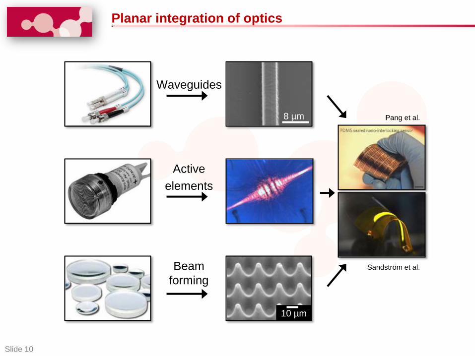
Planar integration of optics
Waveguides
Active
elements
Beam
forming
8 µm
10 µm
Sandström et al.
Pang et al.

Slide 11
Outline
Introduction
Vision of sensor concepts
Materials
Production methods
Characterization
Summary

Slide 12
PlanOS animation

Slide 13
What about future applications?
Movie 3: Application example, biomedicine technology (Lindner, 2014).
Movie 4: Application example, construction surveillance (Lindner, 2014).

Slide 14
Possible and new sensor concepts
Interferometric sensors
Strain detection sensors
Temperature detection sensors
Whispering gallery mode sensors
Planar optical polymer foil spectrometer
Slide 15
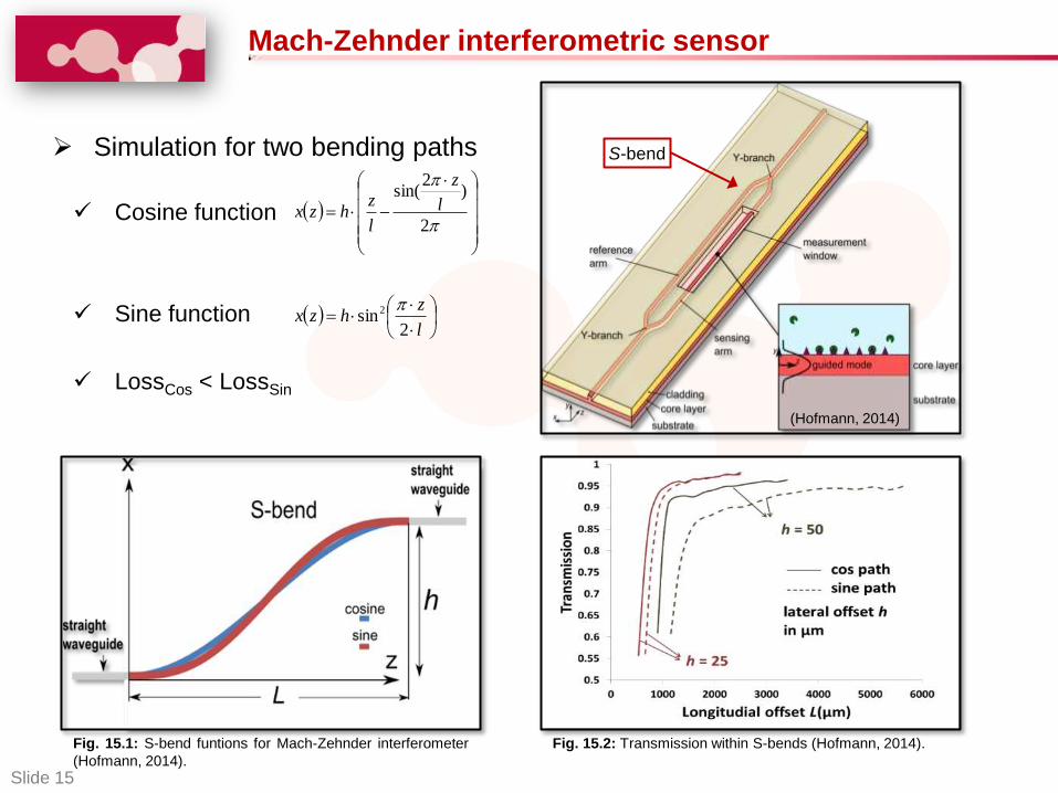
S-bend
Mach-Zehnder interferometric sensor
Simulation for two bending paths
Cosine function
Sine function
LossCos < LossSin
l
zhzx
2sin2
2
)2
sin(l
z
l
zhzx
Fig. 15.1: S-bend funtions for Mach-Zehnder interferometer
(Hofmann, 2014).
Fig. 15.2: Transmission within S-bends (Hofmann, 2014).
(Hofmann, 2014)
Slide 16
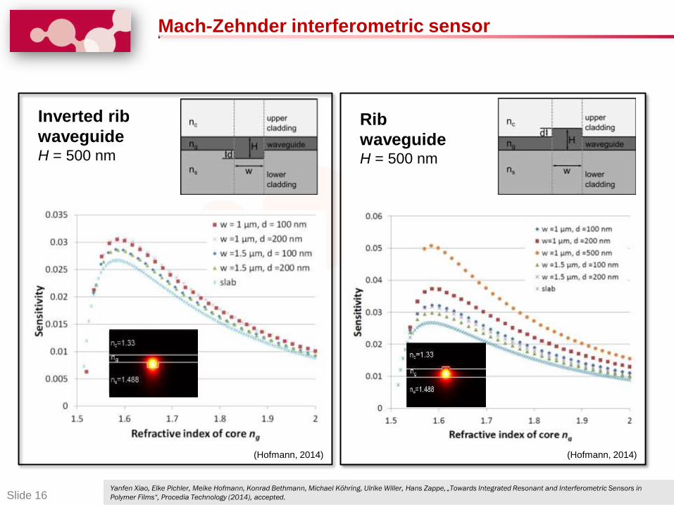
Inverted rib
waveguide H = 500 nm
Rib
waveguide H = 500 nm
Mach-Zehnder interferometric sensor
(Hofmann, 2014) (Hofmann, 2014)
Yanfen Xiao, Elke Pichler, Meike Hofmann, Konrad Bethmann, Michael Köhring, Ulrike Willer, Hans Zappe, „Towards Integrated Resonant and Interferometric Sensors in
Polymer Films“, Procedia Technology (2014), accepted.
Slide 17
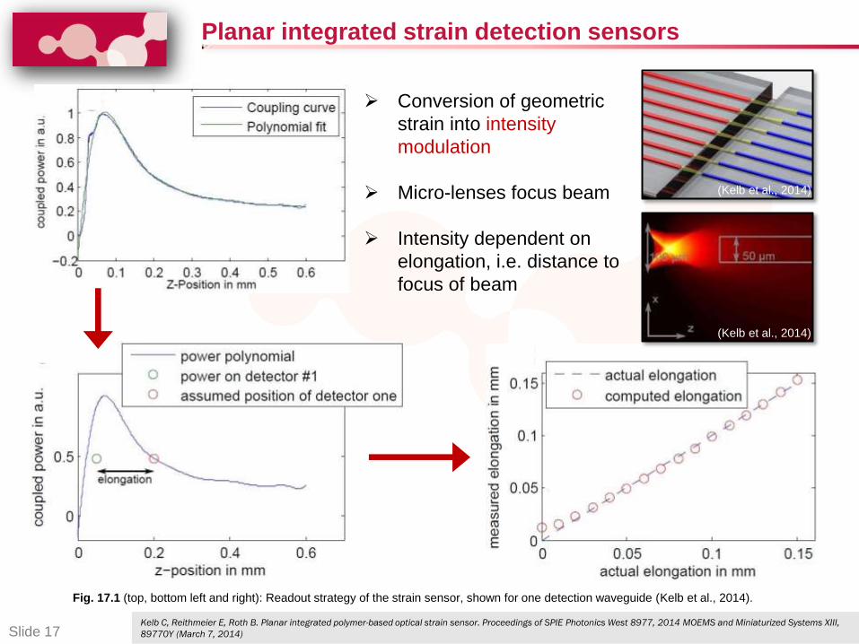
Planar integrated strain detection sensors
Kelb C, Reithmeier E, Roth B. Planar integrated polymer-based optical strain sensor. Proceedings of SPIE Photonics West 8977, 2014 MOEMS and Miniaturized Systems XIII,
89770Y (March 7, 2014)
Fig. 17.1 (top, bottom left and right): Readout strategy of the strain sensor, shown for one detection waveguide (Kelb et al., 2014).
(Kelb et al., 2014)
(Kelb et al., 2014)
Conversion of geometric
strain into intensity
modulation
Micro-lenses focus beam
Intensity dependent on
elongation, i.e. distance to
focus of beam
Slide 18
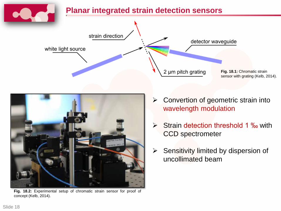
Planar integrated strain detection sensors
Convertion of geometric strain into
wavelength modulation
Strain detection threshold 1 ‰ with
CCD spectrometer
Sensitivity limited by dispersion of
uncollimated beam
Fig. 18.1: Chromatic strain
sensor with grating (Kelb, 2014).
Fig. 18.2: Experimental setup of chromatic strain sensor for proof of
concept (Kelb, 2014).
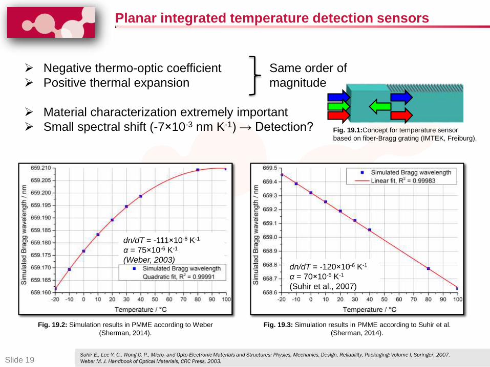
Slide 19
Negative thermo-optic coefficient Same order of
Positive thermal expansion magnitude
Material characterization extremely important
Small spectral shift (-7×10⁻³ nm K-1) → Detection?
dn/dT = -111×10-6 K-1
α = 75×10-6 K-1
(Weber, 2003) dn/dT = -120×10-6 K-1
α = 70×10-6 K-1
(Suhir et al., 2007)
Planar integrated temperature detection sensors
Suhir E., Lee Y. C., Wong C. P., Micro- and Opto-Electronic Materials and Structures: Physics, Mechanics, Design, Reliability, Packaging: Volume I, Springer, 2007.
Weber M. J. Handbook of Optical Materials, CRC Press, 2003.
Fig. 19.2: Simulation results in PMME according to Weber
(Sherman, 2014).
Fig. 19.3: Simulation results in PMME according to Suhir et al.
(Sherman, 2014).
Fig. 19.1:Concept for temperature sensor
based on fiber-Bragg grating (IMTEK, Freiburg).

Slide 20
Whispering gallery mode resonators
Foil integrated Whispering-gallery mode sensors
Resonant frequencies very sensitive to changes
on surrounding refractive index
Ultimate target sensitivity: single-molecule
detection in liquid phase
Figure 20.1: The microsphere is attached to
one waveguide, another waveguide detects the
transmitted signal.
(Wollweber, 2012)
Simulation with RSoft
Ring-resonator: inner diameter 4.5 µm, thickness 1 µm, n=1.59
The left waveguide is used as an excitation source: thickness 1 µm, n=1.46
In case of resonance: light is coupled into the ring-resonator, dip in the transmission signal
Figure 20.2: Build-up of the electromagnetic field in the WGM of a 1 mm thick ring resonator, l = 1089 nm (Petermann, 2014).

Slide 21
Planar optical polymer foil spectrometer - PolyAWG
Simulations for singlemode waveguides
Singlemode waveguide cores with either high
aspect ratio or small dimensions (< 700 nm)
ZnO nanowires in substrate against
mechanical strain
Fig. 21.3: Simulations performed with
PhotonDesing® FIMMWAVE, red bars represent
the single-mode region (TU Clausthal).
Fig. 21.2: Geometry (height x width) of the
simulated waveguides (TU Clausthal).
Koch J., Angelmar M., Schade W.: Arrayed waveguide grating interrogator for fiber Bragg grating sensors: measurement and simulation AO, Vol 51, 7718-7723 (2012).
Fig. 21.1: Sketch of an AWG (TU Clausthal).
multimode
ncore =1.6
singlemode
w
ncore
ncladding = 1.5
h

Slide 22
Decoupling by implementation of ZnO-nanowires
Adding of ammonia and PEI
(polyethylenimine) improved the growth
of ZnO nanowires
Ammonia produces Zn(OH)2 (s)
PEI inhibits the radial growth of the ZnO
nanowires.
Nanoclusters formed in growth solution
can be extracted more easily
Fig. 22.1: SEM image of ZnO nanowires (TU Clausthal). Fig. 22.2: ZnO nanowire growth principle
(TU Clausthal).

Slide 23
Outline
Introduction
Vision of sensor concepts
Materials
Production methods
Characterization
Summary
Slide 24
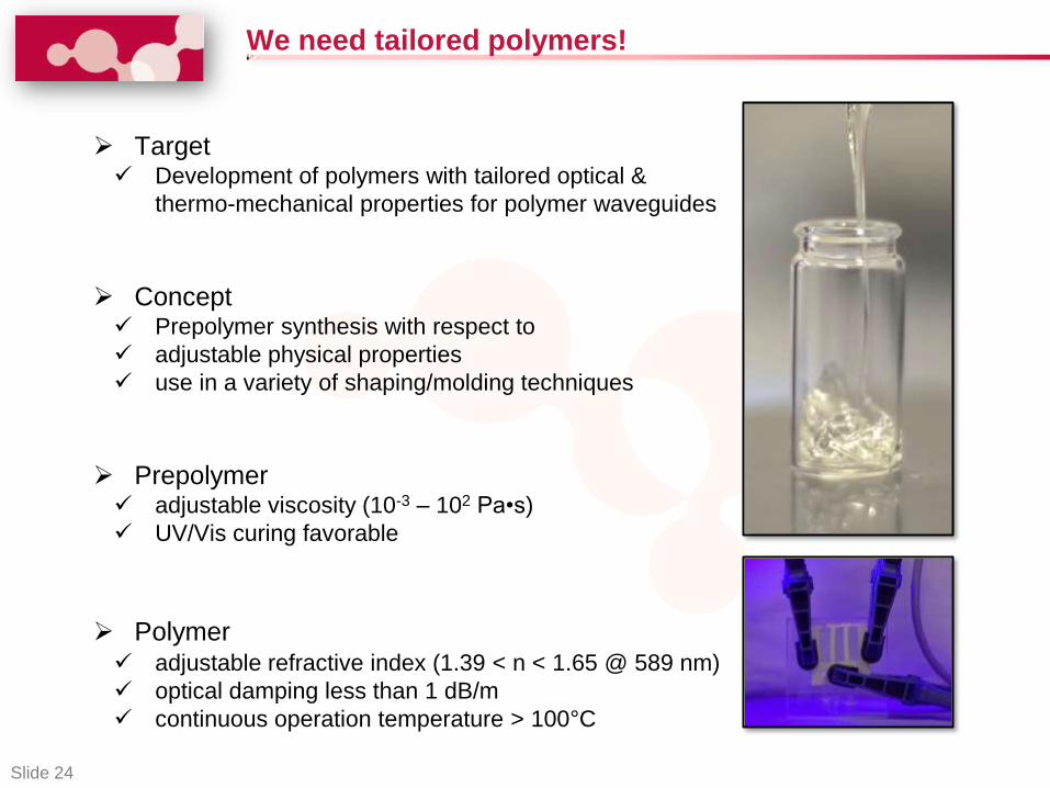
Target Development of polymers with tailored optical &
thermo-mechanical properties for polymer waveguides
Concept Prepolymer synthesis with respect to
adjustable physical properties
use in a variety of shaping/molding techniques
Prepolymer adjustable viscosity (10-3 – 102 Pa•s)
UV/Vis curing favorable
Polymer adjustable refractive index (1.39 < n < 1.65 @ 589 nm)
optical damping less than 1 dB/m
continuous operation temperature > 100°C
We need tailored polymers!

Slide 25
Prepolymer MMA/PMMA/1,3-Butandioldimethacrylate (BDMA)
Polymer Poly(methylmethacrylate-co-1,3-butandioldimethacrylate)
Dopant Phenanthrene
Refractive index tailored hybrid polymers
Fig. 25.2: Refractive index change with dopant
concentration, 1.49 < n < 1.55, @589 nm, 20 °C
(IMTEK, Freiburg).
Fig. 25.1: Viscosity adjustment with prepolymer
concentration, 5 Pa·s > η > 0.15 Pa·s, @100 1/s, 60°C
(IMTEK, Freiburg).
Slide 26
Thermal properties of tailored polymers
OO OO
O
n m
OO
n m
S OO
N3
OO OO
O
n m
CF2
CF2
CF2
CF2
CF2
CF2
CF2
CF3
ON OO
O
n m
OO
n m
S OO
N3
PMMA
Tg
Tg,1
Tg,2
Tdec
Tm
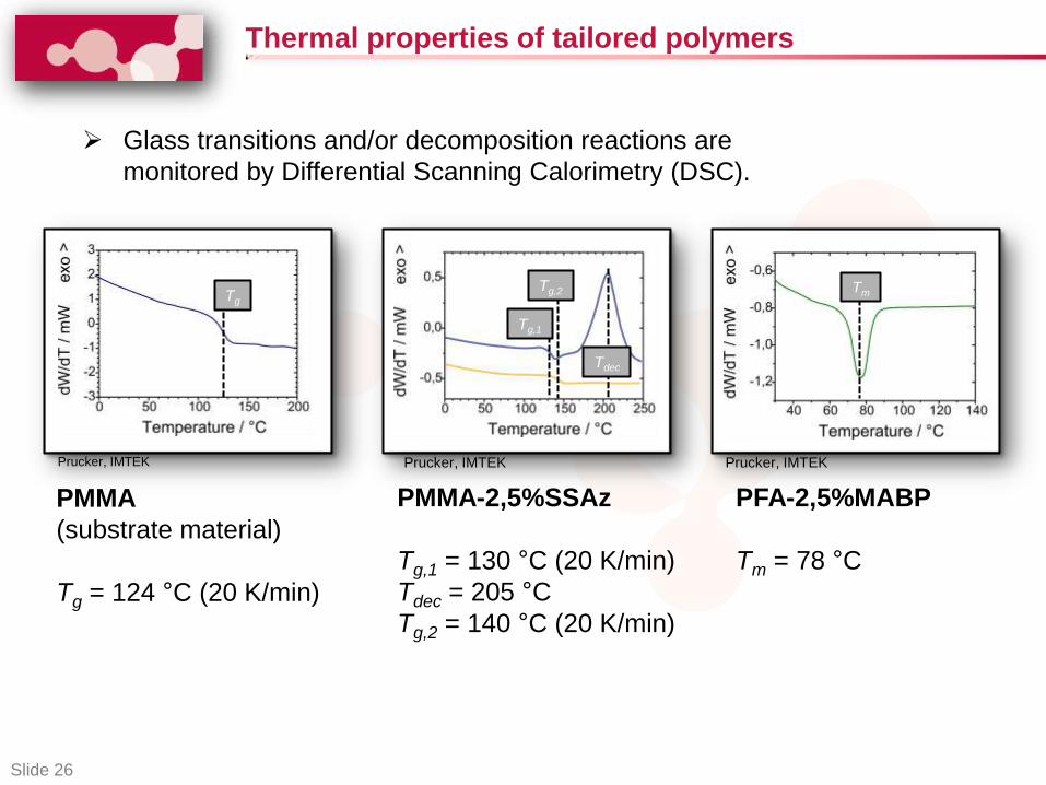
Glass transitions and/or decomposition reactions are
monitored by Differential Scanning Calorimetry (DSC).
PMMA
(substrate material)
Tg = 124 °C (20 K/min)
PMMA-2,5%SSAz
Tg,1 = 130 °C (20 K/min)
Tdec = 205 °C
Tg,2 = 140 °C (20 K/min)
PFA-2,5%MABP
Tm = 78 °C
Prucker, IMTEK Prucker, IMTEK Prucker, IMTEK

Slide 27
TiO2 nanoparticle doped hybrid materials
Molecular weight has strong influence on embedding of
nanoparticles into the polymer matrix
Körner, IMTEK Körner, IMTEK
Körner, IMTEK Körner, IMTEK

Slide 28
Outline
Introduction
Vision of sensor concepts
Materials
Production methods
Characterization
Summary
Slide 29
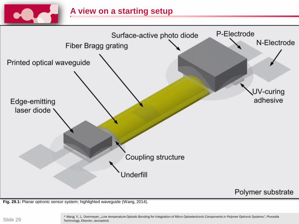
A view on a starting setup
Fig. 29.1: Planar optronic sensor system; highlighted waveguide (Wang, 2014).
* Wang, Y., L. Overmeyer, „Low temperature Optodic Bonding for Integration of Micro Optoelectronic Components in Polymer Optronic Systems“, Procedia
Technology, Elsevier, (accepted).
Slide 30
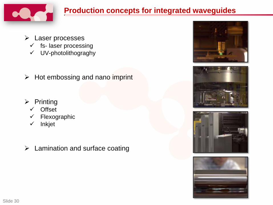
Laser processes fs- laser processing
UV-photolithograghy
Hot embossing and nano imprint
Printing Offset
Flexographic
Inkjet
Lamination and surface coating
Production concepts for integrated waveguides

Slide 31
Direct writing of waveguides – a new approach
P = 400 mW
vwriting = 30 mm/s 10 µm
Fig. 31.1: Direct written structures in PMMA (Pätzold, 2014).
Moving
direction
150 µm
estimated focal spot size
2×10⁷
pulses/spot
2×10⁵
pulses/spot
2×10⁶
pulses/spot
frep = 1 MHz frep = 100 kHz
Epulse = 80 nJ, NA = 0.55, stationary spots 200 µm below surface.
Size grows with decreased
repetition rate
⇒ most likely due to leakage from
Pulse Picker and linear
absorption
Some spots are missing
[1] Pospiech, PhD thesis, Strahlformung in der Femtosekundenlaser-Mikrostrukturierung, 2011.
(Pätzold, 2014)

Slide 32
Polymer processing with fs-laser and UV-lithography
Two-Photon-Polymerization (2PP) Microscope Projection
Photolithography (MPP)
Objective
CCD Camera
Red LED
(Long wavelength)
UV LED
Motorized translation stage XYZ
Chromium Masks
LZH
LZH
LZH

Slide 33
2PP vs. MPP
Fig. 33.3: SEM-image of MPP generated polymer waveguides
(Zywietz, 2014).
Fig. 33.1: Polymer waveguides on a glass substrate
(Zywietz, 2014).
20 µm
2,5 µm
n=1.56 (@ 632 nm)
50 µm
Fig. 33.2: Single polymer waveguide fabricated by 2PP
(Zywietz, 2014).
Fig. 33.4: Polymer waveguides on a highly flexible PMMA
substrate (Zywietz, 2014).
n=1.48 (@ 632 nm)
*Zywietz, U., C. Reinhardt, A.B. Evlyukhin, B.N. Chichkov, „Laser printing of silicon nanoparticles with resonant optical electric and magnetic responses“,
Nature Communications, 5, No. 3402, (2014).
100 µm
n=1.51 (@ 632 nm)
8 mm

Slide 34
Manufacturing of coupling
structures and waveguides in
350 µm-thin polymer foils
Different coupling structures
have been tested
Fig. 34.1: Fabricated optical waveguides
through hot embossing (Rezem, 2014).
Fig. 34.2: Waveguide structures on a
silicone embossing stamp
(Rezem, Akin, 2014)
Hot embossing of micro-optical components
Rezem, M., A. Günther, M. Rahlves, B. Roth, and E. Reithmeier, „Hot embossing of polymer optical waveguides for sensing applications“, Procedia Technology,
Elsevier, (accepted).
Cladding
Cladding
Core
Residual
layer
200 µm
Fig. 34.3: Waveguide transmission
losses as a function of the bend radius
simulated in Zemax and RSoft
(Rezem, 2014).
0
5
10
15
20
25
0,3 0,4 0,5 0,6
Zemax RSoft
Fig. 34.4: Hot-embossing tool currently under development
(Kelb, 2014).
Bend radius [mm]
Tra
nsm
issio
n loss [
dB
]
Slide 35
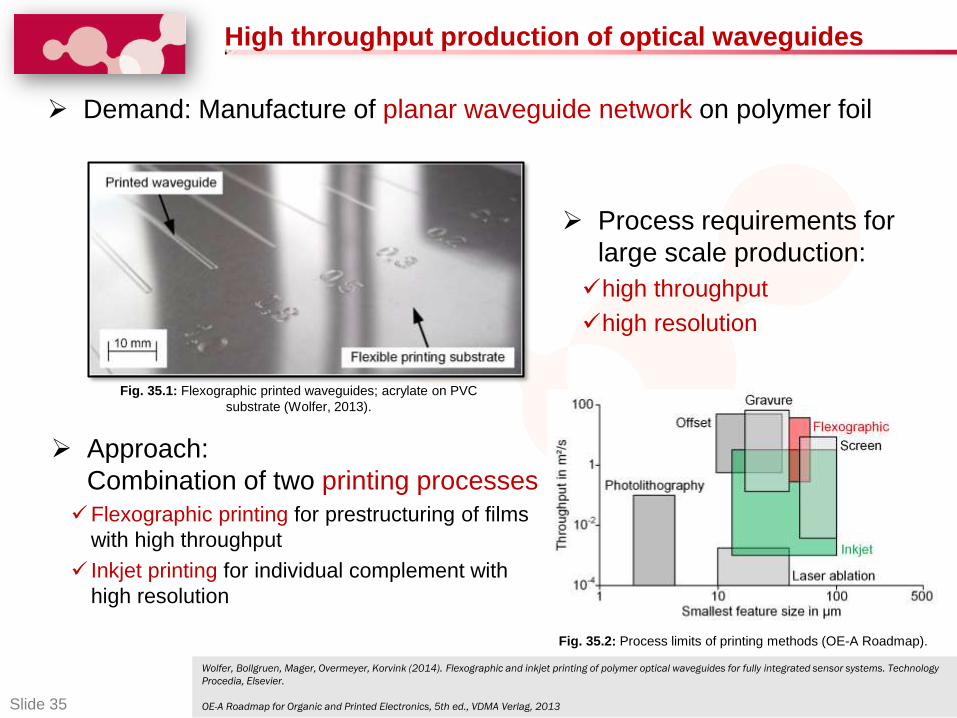
Demand: Manufacture of planar waveguide network on polymer foil
High throughput production of optical waveguides
Fig. 35.1: Flexographic printed waveguides; acrylate on PVC
substrate (Wolfer, 2013).
Wolfer, Bollgruen, Mager, Overmeyer, Korvink (2014). Flexographic and inkjet printing of polymer optical waveguides for fully integrated sensor systems. Technology
Procedia, Elsevier.
OE-A Roadmap for Organic and Printed Electronics, 5th ed., VDMA Verlag, 2013
Process requirements for
large scale production:
high throughput
high resolution
Approach:
Combination of two printing processes
Flexographic printing for prestructuring of films
with high throughput
Inkjet printing for individual complement with
high resolution
Fig. 35.2: Process limits of printing methods (OE-A Roadmap).

Slide 36
Flexographic printing machines
Process development in laboratory scale
Verification on modified industrial scale printing machine
Inkjet printing machines
High throughput production of optical waveguides
Fig. 36.2: Printing machine Speedmaster SM52
(Source: Heidelberger Druckmaschinen AG).
Fig. 36.4: Dimatix DMP 2831 (Source: Dimatix)
OE-A Roadmap for Organic and Printed Electronics, 5th ed., VDMA Verlag, 2013
Fig. 36.1: Flexographic printing machine in
laboratory scale, IGT F1 UV
Fig. 36.3: Pixdro LP 50 (Source: Meyer Burger)

Slide 37
High throughput production of optical waveguides
Flexographic printing sequence:
1. Inking of anilox
2. Polymer transfer to printing plate
3. Mirror inverted reproduction on
substrate
Additive manufacturing for cost and
resource efficiency
Process chain from layout to printing results:
Wolfer, Overmeyer (2013): Flexographic Printing of Polymer Optical Waveguides, Proceedings of the Distributed Intelligent Systems and Technologies Workshop, St.
Petersburg, Russia, July 1-4.
Fig. 37.1: Operating principle of flexographic printing
(Wolfer, 2013).
Fig. 37.2: Process chain from layout to print results (Wolfer, 2014).

Slide 38
Printing of multimode optical waveguides
Waveguide setup in layers with parabolic shape
High throughput production of optical waveguides
Fig. 38.1: Computed 3D model of printed waveguide
(Wolfer, 2013).
Fig. 38.2: Possible waveguide concepts by combining the core and cladding layers (Wolfer, 2014).
Wolfer, Bollgruen, Mager, Overmeyer, Korvink (2014). Flexographic and inkjet printing of polymer optical waveguides for fully integrated sensor systems. Technology
Procedia, Elsevier.
Property Value
Width 20-1,000 mm
Height 4-110 mm
max. Aspect ratio 0.5
Speed of operation 50-260 m²/h
Surface roughness 12.5 nm
Table 2: Typically achieved process properties (Wolfer, 2014).
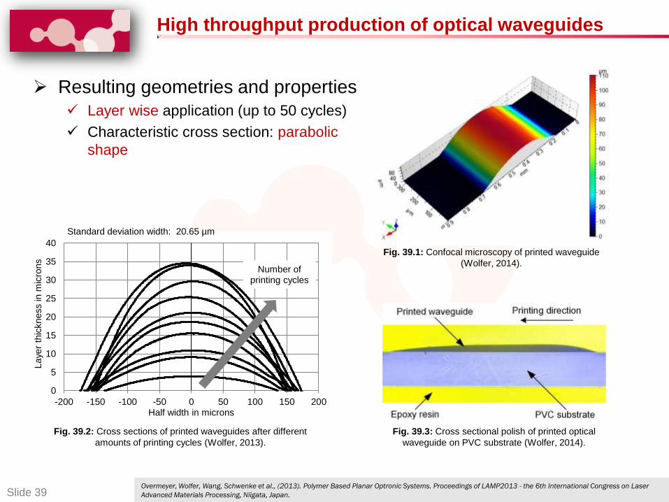
Slide 39
High throughput production of optical waveguides
Fig. 39.3: Cross sectional polish of printed optical
waveguide on PVC substrate (Wolfer, 2014).
Resulting geometries and properties
Layer wise application (up to 50 cycles)
Characteristic cross section: parabolic
shape
Overmeyer, Wolfer, Wang, Schwenke et al., (2013). Polymer Based Planar Optronic Systems. Proceedings of LAMP2013 - the 6th International Congress on Laser
Advanced Materials Processing, Niigata, Japan.
0
5
10
15
20
25
30
35
40
-200 -150 -100 -50 0 50 100 150 200
Laye
r th
ickn
ess in
mic
rons
Half width in microns
Number ofprinting cycles
Fig. 39.2: Cross sections of printed waveguides after different
amounts of printing cycles (Wolfer, 2013).
Standard deviation width: 20.65 µm
Fig. 39.1: Confocal microscopy of printed waveguide
(Wolfer, 2014).

Slide 40
Simulation of printed waveguides
Multiple printing cycles lead to:
Larger contact angle
Higher waveguide geometry
Geometry susceptible to manipulation
Ray tracing simulation to estimate
and optimize optical attenuation
Ray tracing using Zemax
Source @ 638 nm
Numerical aperture 0.27
Contact angle variation 15-90 degree
Fig. 40.2: Ray tracing simulation (Zemax), light intensity in dependence of contact angle and waveguide heigth (Wolfer, 2014).
Fig. 40.1: Optical attenuation vs. contact angle according
to ray tracing simulation (Wolfer, 2014).

Slide 41
Approach for smoother surfaces: self alignment of polymer by local
variation of surface energy
Decrease of surface
roughness
Decrease of lateral
undulations
Higher contact angle
Higher aspect ratio
Lower attenuation expected
Sources of roughness
Substrate surface
Interface of core layers
Interface core/cladding
Considered in ray tracing as
Gaussian scattering
Fig. 41.1: Ray tracing simulation (Zemax), roughness
considered as Gaussian scattering (Wolfer, 2014).
10 mm
substrate
Fig. 41.2: Left: Conditioned PVC substrate with distributed acrylate. Right:
Confocal miscroscopy of self aligned polymer (acrylate)
Raw PVC
substrate
Lines for local
variation of
surface energy
(acrylate)
Printing varnish
(acrylate)
1 mm
Simulation of printed waveguides

Slide 42
Successful lamination of COC and
PMMA foils using an interlayer of a
sulfonazide containing polymer
Production of nano-composites and
continuous transitions from polymer to
oxide with sputtering methods
Ta2O5 nano-particles produced by a gas
aggregation source on a layer of ion-
beam sputtered PTFE
The size of the nano-particles is between
16 nm and 24 nm
Reactive lamination and functionalized surfaces
Fig. 42.1: Partially laminated COC and PMMA foils (Rother,
2014).
Fig. 49: SEM image of Ta2O5 nanoparticles (Gauch, 2014).
Fig. 42.3: SEM image of Ta2O5 nanoparticles (Gauch, 2014).
Fig. 42.2: Ion beam sputtering (Gauch, 2014).

Slide 43
What about active optical systems?
Fig. 43.1: Planar optronic sensor system; highlighted diodes (Wang, 2014).

Slide 44
High success rate
95 %
Short process time
app. 10 s
Mechanical strength
23 N/mm2
Electrical conductivity
panacol 4732: 0.292 Ω
Dymax OP-29: 0.169 Ω
Dymax OP-29-Gel: 0.112 Ω
Dymax OP-24-Rev-B: 0.110 Ω
Delo GB368: 0.286 Ω
Vacuum
Chip
UV-curing
adhesive
Transparent
polymer substrate
UV-radiation
Mirror
UV reflective coating
Bonding
head
UV LED lamp
Bonding head
Optodic bonding as bridging technology
Fig. 44.1 (right): Schematic illustration
of optode for sideway irradiation
(Wang, 2014)
Fig. 44.2: Photo of realized optode, (Low Temperature Optodic Bonding for
Integration of Micro Optoelectronic Components in Polymer Optronic
Systems, Wang et al., SysInt 2014, accepted).

Slide 45
Fig. 45.3: Bare Laser diode
CHIP-650-P5 (Wang 2013). Fig. 45.4: Image from confocal
microscopy (Wolfer and Wang 2013).
Optical coupling of single mode waveguide
Thickness < 1 µm
Challenge
Optodic bonding as bridging technology
Success r
ate
in %
Irradiation time in s
100
90
80
70
60
50
40
30
20
10
0 70s 50s 30s 10s 5s 3s
Arith
metic m
ean a
nd
sta
ndard
devia
tion in O
hm
Irradiation time in s
1,0
0,9
0,8
0,7
0,6
0,5
0,4
0,3
0,2
0,1
0 70s 50s 30s 10s 5s 3s
Fig. 45.2: Electric resistance of optodic bonded chips dependent on
irradiation time, intensity of 7070 mW/cm2 (Wang, 2014)
Fig. 45.1: Success rate of optodic bonded chips dependent on
irradiation time, intensity of 7070 mW/cm2 (Wang, 2014)
Slide 46
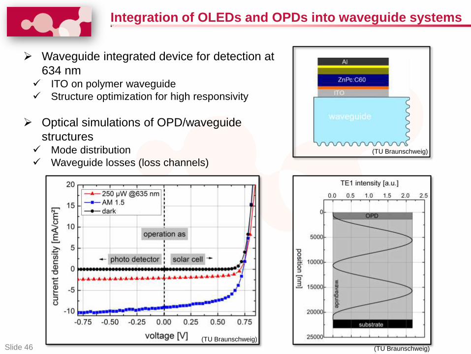
Waveguide integrated device for detection at
634 nm ITO on polymer waveguide
Structure optimization for high responsivity
Optical simulations of OPD/waveguide
structures Mode distribution
Waveguide losses (loss channels)
Integration of OLEDs and OPDs into waveguide systems
(TU Braunschweig)
(TU Braunschweig)
(TU Braunschweig)
Slide 47
Photodetector operation parameters
1E-5 1E-4 1E-3 0.01 0.1 1 10 100 1000
1E-3
0.01
0.1
1
10
100
cu
rre
nt [µ
A]
power [µW]
Device
D2
B2
B1
Measured @ 635 nm
Dark current:
1 nA (best)
= 33 nA/cm²
Responsivity:
320 mA/W @ -1V
63% EQE, commercial
Si ~ 80%
Bandwidth:
1 MHz
(limited by setup)
0 1 2 3 40.00
0.01
0.02
0.03
0.04@ 300 kHz
RC
= 0,35 µs
voltage [m
V]
time [µs]
RC
= 0,4 µs
102
103
104
105
106
107
1
10
voltage [V
]
f [Hz]
3 dB
(TU Braunschweig)
(TU
Braunschweig)
(TU
Braunschweig)
T. Otto, T. Rabe, S. Döring, W. Kowalsky, “Organic Solar Cells as Polymer Waveguide integrated Photodetectors”, Procedia Technology, 2014, (accepted)

Slide 48
Laser-active waveguides
Laser
NP
Liquid
Fig. 48.1: Laser-active
nanoparticle generation
(Sajti, 2013).
Fig. 48.2:
Homogenous particle
embedding (Sajti,
2013).
Fig. 48.3: Laser-active
polymer waveguide
(Sajti, 2013).
Fig. 48.4: Flexible laser
module (Kwon et al., 2008).
Nd:YVO4; 0.1 wt% Nd ablated in water 0.1 wt%
Nd ablated in Acetone 1 wt%
inte
nsity [
a.u
.]
emission wavelength [nm]
Fig. 48.7: SEM-image of Nd:KGW
embedded ormosil waveguide (Sajti, 2013). Fig. 48.5: Laser-active particles
in colloidal (Sajti, 2013). form
Nd:KGW nanocrystals dispersed waveguide
Fig. 48.6: Size distribution of
laser-active particles (Sajti, 2013).
nanoparticle size [nm]
rel. f
requency [a.u
.]
5 µm
300 µm
Kwon, Y.K., J.K. Han, J.M. Lee, Y.S. Koo, J.H. Oh, H.-S. Lee, E.-H. Lee, „Organic–inorganic hybrid materials for flexible optical waveguide applications“, J. Mater. Chem.,
18, 579-585, DOI: 10.1039/B715111J, (2008).

Slide 49
Outline
Introduction
Vision of sensor concepts
Materials
Production methods
Characterization
Summary
Slide 50
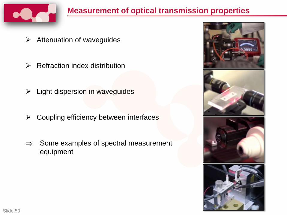
Measurement of optical transmission properties
Attenuation of waveguides
Refraction index distribution
Light dispersion in waveguides
Coupling efficiency between interfaces
Some examples of spectral measurement
equipment

Slide 51
Light sources
LED, including confocal pattern for end face characterization
Diode laser (638 nm, 140 mW)
Numerical aperture steplessly
variable within 0.1-0.5
Aperture sizes: 1-1,000 mm
Identification of length-independent attenuation
Fig. 51.2: Optical measurement setup (Dumke, ITA, 2014).
Wolfer, Bollgruen, Mager, Overmeyer, Korvink (2014). Flexographic and inkjet printing of polymer optical waveguides for fully integrated sensor systems. Technology
Procedia, Elsevier (accepted).
Fig. 51.1: End face of printed waveguide in optical
measurement setup with focused LED spot
(Wolfer, 2014).

Slide 52
Ellipsometer (Sentech)
Thickness and refractive index measurement of thin
Layers (up to 100 µm)
Operating Wavelength 280 – 1700 nm
Refractive Index Profilometer (Rinck)
Refractive index measurements of transparent materials
Different wavelengths (405, 635, 850, and 1320 nm)
Measurement area: 500 µm x 500 µm
FTIR-spectrometer with
halogen light source
Light source: Xe-lamp (UV/VIS)
Goniometer Sample stage
Analyzer
Autocollimation-
scope
Fig. 52.2: Refractive Index Profilometer
(Günther, 2014).
Fig. 52.1: FTIR Ellipsometer Sentech SE 850 (Kelb, 2014).
Optical characterization in cleanroom environment
Lens
Sample stage
Sample
Reference
glass Detector

Slide 53
Fig. 53.1: Epocore waveguides structured on a silicon
wafer (Günther, 2014).
Fig. 53.2: Waveguide written by laser direct writing
into the substrate (Günther, 2014).
Refractive index measurements
fs-laser direct writing Hot embossing
Reference glass (n = 1.51)
Immersion oil (n = 1.497)
SiO2 (n=1.456)
Epocore waveguide
(n = 1.451)
100 mm
50
mm
Substrate
(n = 1.501)
Waveguide
(n = 1.53 - 1.66)
6 mm
3 m
m
Epocore waveguides
structured on a silicon wafer Substrate: silicon
Core material: epocore
Resolution 1.25 µm/pixel
Profilometer specifications Refractive index resolution up to 10-4
Spatial resolution: 0.5 µm
Wavelength: 405 nm, 635 nm, 845 nm,
1320 nm

Slide 54
Outline
Introduction
Vision of sensor concepts
Materials
Production methods
Characterization
Summary

Slide 55
Sensors for excellent flight performances …
Fig. 55.1: Illustration of nerve tracks on bat wing
(Türk, 2014).

Slide 56
… and for stress and temperature surveillance
Fig. 56.1: Illustration of planar sensor foil on airplane
wing (Türk, 2014).
Movie 5: Application example, structural monitoring of wing (Lindner, 2014).

Slide 57
Summary
Planar sensors concepts for measurement of Temperature
Strain
Liquid and gaseous analytes
Development of thermo-mechanical and chemical
stable as well as refractive index tailored polymers
High throughput production of waveguides in reel-
to-reel process - a combination of Printing
Hot embossing
Laser processing
Lithography
Optodical bonding as bridging technology
Equipment available for characterization of Refractive index
Thickness
Attenuation
Form stability
Glass transition temperature

Slide 58
The PlanOS science team (alphabetical order):
Meriem Akin, Tobias Birr, Patrick Bollgrün, Kort Bremer, Wei Cheng, Boris
Chichkov, Ayhan Demircan, Sebastian Dikty, Sebastian Döhring, Henrik
Ehlers, Ludmila Eisner, Farzaneh Fattahi Comjani, Melanie Gauch, Uwe
Gleissner, Axel Günther, Thomas Hanemann, Meike Hofmann, Dominik
Hoheisel, Kirsten Honnef, Christian Kelb, Ann-Katrin Kniggendorf, Michael
Köhring, Martin Körner, Jan Gerrit Korvink, Wolfgang Kowalsky, Tobias
Krühn, Dario Mager, Uwe Morgner, Claas Müller, Gregor Osterwinter,
Torsten Otto, Ludger Overmeyer, Malwina Pajestka, Welm Pätzold, Ann
Britt Petermann, Elke Pichler, Oswald Prucker, Torsten Rabe, Maik
Rahlves, Holger Reinecke, Carsten Reinhardt, Eduard Reithmeier, Maher
Rezem, Lutz Rissing, Detlef Ristau, Raimund Rother, Bernhard Roth,
Jürgen Rühe, Laszlo Sajti, Wolfgang Schade, Thomas Schmidt, Anne-
Katrin Schuler, Andreas Schwenke, Andreas Seifert, Stanislav Shermann,
Yixiao Wang, Ulrike Willer, Tim Wolfer, Merve Wollweber, Hans Zappe,
and Urs Zywietz.
Funded by German Research Foundation
(Deutsche Forschungsgemeinschaft)
Acknowledgements