Embed Size (px)
Citation preview
HAL Id: hal-01098616https://hal.inria.fr/hal-01098616
Submitted on 27 Dec 2014
HAL is a multi-disciplinary open accessarchive for the deposit and dissemination of sci-entific research documents, whether they are pub-lished or not. The documents may come fromteaching and research institutions in France orabroad, or from public or private research centers.
L’archive ouverte pluridisciplinaire HAL, estdestinée au dépôt et à la diffusion de documentsscientifiques de niveau recherche, publiés ou non,émanant des établissements d’enseignement et derecherche français ou étrangers, des laboratoirespublics ou privés.
On Transfer Functions Realizable with Active ElectronicComponents
Laurent Baratchart, Sylvain Chevillard, Fabien Seyfert
To cite this version:Laurent Baratchart, Sylvain Chevillard, Fabien Seyfert. On Transfer Functions Realizable with ActiveElectronic Components. [Research Report] RR-8659, Inria Sophia Antipolis; INRIA. 2014, pp.36. hal-01098616
ISS
N02
49-6
399
ISR
NIN
RIA
/RR
--86
59--
FR+E
NG
RESEARCHREPORTN° 8659December 2014
Project-Team Apics
On Transfer FunctionsRealizable with ActiveElectronic ComponentsLaurent Baratchart, Sylvain Chevillard, Fabien Seyfert

RESEARCH CENTRESOPHIA ANTIPOLIS – MÉDITERRANÉE
2004 route des Lucioles - BP 9306902 Sophia Antipolis Cedex
On Transfer Functions Realizable with ActiveElectronic Components
Laurent Baratchart, Sylvain Chevillard, Fabien Seyfert
Project-Team Apics
Research Report n° 8659 — December 2014 — 36 pages
Abstract: In this work, we characterize transfer functions that can be realized with standardelectronic components in linearized form, e.g. those commonly used in the design of analog am-plifiers (including transmission lines) in the small signal regime. We define the stability of suchtransfer functions in connection with scattering theory, i.e. in terms of bounded reflected poweragainst every sufficiently large load. In the simplest model for active elements, we show that un-stable transfer functions exist which have no pole in the right half-plane. Then, we introduce morerealistic transfer functions for active elements which are passive at very high frequencies, and weshow that they have finitely many poles in the right half-plane. Finally, in contrast to the idealtransfer functions studied before, the stability of such “realistic” transfer functions is character-ized by the absence of poles in the open right half-plane and the positivity of the real part of theresidues of the poles located on the imaginary axis.This report is written in a way which is suitable to the non-specialist, and every notion is definedand analyzed from first principles.
Key-words: Amplifier, transfer function, active components, transistor, diode, transmission line,negative resistor, stability, Hardy spaces.
Sur les fonctions de transfert réalisables avec descomposants électriques actifs
Résumé : Dans ce travail, nous caractérisons les fonctions de transfert qui peuvent êtresynthétisées avec des composants électroniques standards linéarisés, y compris des lignes detransmission. Ce sont les composants typiquement utilisés pour la synthèse d’amplificateursanalogiques, modélisés en régime « faible signal ». Nous définissons la stabilité de telles fonctionsde transfert en nous appuyant sur la théorie de dispersion des ondes, précisément en demandantà ce que la puissance réfléchie contre toute charge suffisamment grande reste bornée vis-à-vis dela fréquence. Nous montrons qu’il existe des fonctions de transfert qui sont instables mais n’ontpas de pôle dans le demi-plan droit. Nous introduisons ensuite une modélisation plus réalistedes fonctions de transfert des composants actifs, pour traduire l’hypothèse réaliste selon laquelleils deviennent passifs à très haute fréquence. Nous montrons que les circuits synthétisables avecde tels composants réalistes ont un nombre fini de pôles dans le demi-plan droit ; en outre,nous montrons qu’on peut caractériser la stabilité des fonctions de transfert ainsi obtenues parl’absence de pôle dans le demi-plan droit ouvert et le fait que les résidus des pôles situés sur l’axeimaginaire aient une partie réelle positive.
Ce rapport est écrit de telle façon qu’il soit accessible au non spécialiste et chaque notion estdéfinie et étudiée à partir de notions élémentaires.
Mots-clés : Amplificateur, fonction de transfert, composants actifs, transistor, diode, ligne detransmission, résistance négative, stabilité, espaces de Hardy.
Transfer functions realizable with active electronic components 3
Contents1 Introduction 3
2 Electronic components under consideration 42.1 Dipoles . . . . . . . . . . . . . . . . . . . . . . . . . . . . . . . . . . . . . . . . . 42.2 Transmission lines . . . . . . . . . . . . . . . . . . . . . . . . . . . . . . . . . . . 52.3 Diodes . . . . . . . . . . . . . . . . . . . . . . . . . . . . . . . . . . . . . . . . . . 52.4 Transistors . . . . . . . . . . . . . . . . . . . . . . . . . . . . . . . . . . . . . . . 5
3 Structure of circuits 7
4 Partial transfer functions 94.1 Partial transfer from a current source . . . . . . . . . . . . . . . . . . . . . . . . 94.2 Partial transfer from a voltage source . . . . . . . . . . . . . . . . . . . . . . . . . 10
5 R-L-C circuits with negative resistors 115.1 What the inverter makes possible . . . . . . . . . . . . . . . . . . . . . . . . . . . 125.2 Frequency response of RLC circuits with negative resistors . . . . . . . . . . . . . 12
6 Circuits with transmission lines 136.1 Using transmission lines as one-port circuits . . . . . . . . . . . . . . . . . . . . . 146.2 Composing one-port circuits . . . . . . . . . . . . . . . . . . . . . . . . . . . . . . 156.3 Class of all impedances of one-port circuits . . . . . . . . . . . . . . . . . . . . . 17
7 Notion of stability 18
8 Realistic model of linearized components 22
9 A stability criterion 27
10 Appendix 1: Telegrapher’s equation 28
11 Appendix 2: Transfer functions and stability 30
AcknowledgmentsThe research presented in this report has been partially funded by the CNES through thegrant R&T RS 10/TG1-019. We wish to thank Juan-Mari Collantes from Universidad del PaísVasco/Euskal Herriko Unibertsitatea for his patient advice and for the long discussions we hadwith him regarding the stability of electronic circuits.
1 IntroductionIn this work, we characterize transfer functions that can be realized with standard electroniccomponents in linearized form, e.g. those commonly used in the design of analog amplifiers(including transmission lines) in the small signal regime. We define the stability of such transferfunctions in connection with scattering theory, i.e. in terms of bounded reflected power againstevery sufficiently large load. In the simplest model for active elements, we show that unstabletransfer functions exist which have no pole in the right half-plane. Then, we introduce more
RR n° 8659
4 L. Baratchart, S. Chevillard & F. Seyfert
realistic transfer functions for active elements which are passive at very high frequencies, andwe show that they have finitely many poles in the right half-plane. Finally, in contrast tothe ideal transfer functions studied before, the stability of such “realistic” transfer functions ischaracterized by the absence of poles in the open right half-plane and the positivity of the realpart of the residues of the poles located on the imaginary axis.
This report is written in a way which is suitable to the non-specialist, and every notion isdefined and analyzed from first principles.
2 Electronic components under considerationIn this section, we give a detailed account of elementary ideal models for electronic componentsthat we consider, along with equations satisfied by currents and voltages at their terminals.These equations are expressed in terms of complex impedances and admittances [2, 3], i.e. weexpress the relations between Laplace transforms of these currents and voltages, see Section 11for definitions. We denote Laplace transforms with uppercase symbols, e.g. V = V (s) is afunction of a complex variable s which stands for the Laplace transform of the voltage v = v(t)which is a function of the time t.
By convention, we always orient currents so that they enter electronic components.
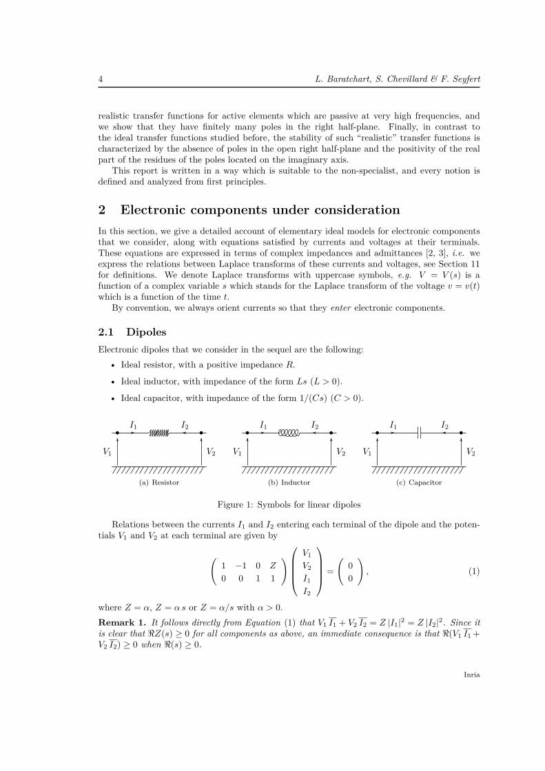
2.1 DipolesElectronic dipoles that we consider in the sequel are the following:
• Ideal resistor, with a positive impedance R.
• Ideal inductor, with impedance of the form Ls (L > 0).
• Ideal capacitor, with impedance of the form 1/(Cs) (C > 0).
(a) Resistor (b) Inductor (c) Capacitor
Figure 1: Symbols for linear dipoles
Relations between the currents I1 and I2 entering each terminal of the dipole and the poten-tials V1 and V2 at each terminal are given by
(1 −1 0 Z
0 0 1 1
)V1
V2
I1
I2
=(
00
), (1)
where Z = α, Z = α s or Z = α/s with α > 0.Remark 1. It follows directly from Equation (1) that V1 I1 + V2 I2 = Z |I1|2 = Z |I2|2. Since itis clear that <Z(s) ≥ 0 for all components as above, an immediate consequence is that <(V1 I1 +V2 I2) ≥ 0 when <(s) ≥ 0.
Inria

Transfer functions realizable with active electronic components 5
2.2 Transmission linesTransmission lines are distributed components: they are viewed as a series of infinitesimal resis-tors, capacitors and inductors which is usually modeled by telegrapher’s equation [9, sec. 9.7.3],see the discussion in Section 10. All transmission lines in a circuit are assumed to share the sameground. The latter is often implicit and is not drawn along with the symbol for a transmissionline. In Section 6, it will be convenient to materialize the current loss between terminals of a lineas resulting from a current occurring in a wire (which does not actually exist) connected to theground. This virtual wire is drawn with a dotted segment on Figure 2. One may ignore it, inwhich case one should ignore as well the last row and the last column of the matrix in Figure 2.
The behavior of a transmission line is otherwise linear and characterized by the relationsin Figure 2. In the matrix shown there, γ =
√(R+ Ls)(G+ Cs) is sometimes called the
propagation coefficient (note it is frequency-dependent) while z0 = (R + Ls)/γ is the so-calledcharacteristic impedance of the line (cf. Section 10). Here R, G, L and C are nonnegativenumbers.
−1 0 z0 coth(γ) z0
sinh(γ) 0
0 −1 z0
sinh(γ) z0 coth(γ) 0
0 0 1 1 1
V1
V2
I1
I2
I3
=
000
Figure 2: Symbol and relations for transmission lines
2.3 DiodesNext we consider diodes. A commonly accepted model of the diode assumes that the relationbetween the current i traversing the diode and the voltage u is given as a relation i = f(u)where f is a non linear real-valued function. In particular, one assumes that the diode has noinductive nor capacitive effect (f only depends on u and not on du/dt nor di/dt). We only studysmall perturbations around a polarization point (u(Q), i(Q)), hence it is legitimate to linearizethe behavior of the diode, which gives us
i− i(Q) = g · (u− u(Q)), g = dfdu (u(Q)).
Hereafter we rename i− i(Q) as i and u− u(Q) as u. That is, although the variables of interestto the linearized model of the diode are incremental rather than absolute electrical quantities,we denote them like any other intensity or voltage for notational homogeneity. Taking Laplacetransforms we get I = g U , so the (linearized) diode appears as a standard linear dipole withadmittance g ∈ R. Typical in our context are tunnel diodes which behave (once correctlypolarized) as ideal negative resistors: g < 0. The symbol we use for, as well as the relationssatisfied by linearized diodes are summarized in Figure 3.
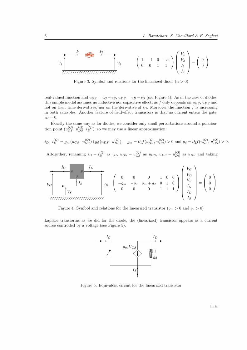
2.4 TransistorsOur circuits may also contain transistors. Specifically, we consider field-effect transistors. Thesehave three terminals called gate, source, and drain (denoted respectively by G, S and D). Thebehavior is usually described by a relation of the form iD = f(uGS , uDS) where f is a non-linear
RR n° 8659
6 L. Baratchart, S. Chevillard & F. Seyfert
(1 −1 0 −α0 0 1 1
)V1
V2
I1
I2
=(
00
)
Figure 3: Symbol and relations for the linearized diode (α > 0)
real-valued function and uGS = vG− vS , uDS = vD− vS (see Figure 4). As in the case of diodes,this simple model assumes no inductive nor capacitive effect, as f only depends on uGS , uDS andnot on their time derivatives, nor on the derivative of iD. Moreover the function f is increasingin both variables. Another feature of field-effect transistors is that no current enters the gate:iG = 0.
Exactly the same way as for diodes, we consider only small perturbations around a polariza-tion point (u(Q)
GS , u(Q)DS , i
(Q)D ), so we may use a linear approximation:
iD−i(Q)D = gm (uGS−u(Q)
GS )+gd (uDS−u(Q)DS ), gm = ∂1f(u(Q)
GS , u(Q)DS ) > 0 and gd = ∂2f(u(Q)
GS , u(Q)DS ) > 0.
Altogether, renaming iD − i(Q)D as iD, uGS − u
(Q)GS as uGS , uDS − u
(Q)DS as uDS and taking
0 0 0 1 0 0−gm −gd gm + gd 0 1 0
0 0 0 1 1 1
VG
VD
VS
IG
ID
IS
=
000
Figure 4: Symbol and relations for the linearized transistor (gm > 0 and gd > 0)
Laplace transforms as we did for the diode, the (linearized) transistor appears as a currentsource controlled by a voltage (see Figure 5).
Figure 5: Equivalent circuit for the linearized transistor
Inria

Transfer functions realizable with active electronic components 7
3 Structure of circuitsFormally speaking, a circuit is a directed graph with labeled vertices meeting the followingconstraints:
• There are two kinds of vertices: electronic components and junction nodes.
• A junction node has degree greater or equal to 2.
• An electronic component labeled as a resistor, capacitor, inductor, diode or transmissionline has exactly degree 2.
• An electronic component labeled as a transistor has exactly degree 3.
• An electronic component can only be adjacent with a junction node and reciprocally.
• The edges are oriented from junction nodes to electronic components (this definition isnon-ambiguous and applies to all edges because of the previous rule).
We number the junction nodes and the edges. Without loss of generality, we can supposethat edges adjacent to a given electronic component are numbered consecutively (because anedge is adjacent to one and only one such component), and that the ordering gate-drain-sourceprevails in the case of transistors.
To each junction node j is associated a potential Vj and to each edge k is associated anelectric current Ik. One junction node is called ground (its potential is 0 by convention andwithout loss of generality, we suppose that it is numbered as vertex 1). An example of circuit isgiven in Figure 6: electronic components are represented with their specific symbols introducedin Section 2, but they should now be understood as vertices of the graph. Junction nodes areindicated with bullets, except for the ground which is represented the usual way. For clarity, theground is represented at multiple places on the figure, but it should be seen as a single vertex.
Figure 6: Example of a circuit
Let us denote by X = t(V1, . . . , Vn, I1, . . . , Ip) the vector made of all potentials and currentsof a circuit. Theses quantities are related as follows.
• The ground potential is 0: V1 = 0.
• For each junction node k distinct from the ground, Kirchhoff’s first law holds:∑edge j adjacent to k
Ij = 0.
RR n° 8659
8 L. Baratchart, S. Chevillard & F. Seyfert
The ground is here excluded because currents may exist between transmission lines andthe ground, though they are not figured on the graph representing the circuit.
• For each electronic component k, relations from Section 2 between potentials at junctionnodes adjacent to the component and currents entering the component must be satisfied.
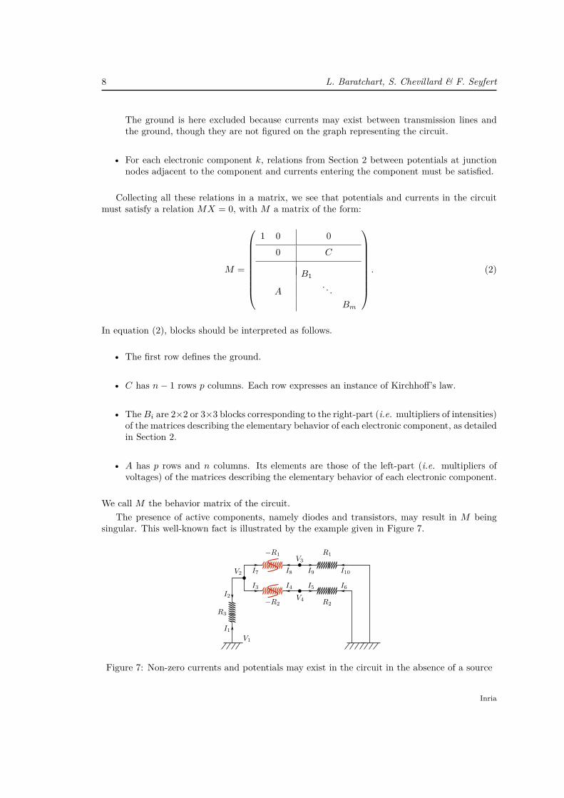
Collecting all these relations in a matrix, we see that potentials and currents in the circuitmust satisfy a relation MX = 0, with M a matrix of the form:
M =
1 0 0
0 C
B1
A. . .
Bm
. (2)
In equation (2), blocks should be interpreted as follows.
• The first row defines the ground.
• C has n− 1 rows p columns. Each row expresses an instance of Kirchhoff’s law.
• The Bi are 2×2 or 3×3 blocks corresponding to the right-part (i.e. multipliers of intensities)of the matrices describing the elementary behavior of each electronic component, as detailedin Section 2.
• A has p rows and n columns. Its elements are those of the left-part (i.e. multipliers ofvoltages) of the matrices describing the elementary behavior of each electronic component.
We call M the behavior matrix of the circuit.The presence of active components, namely diodes and transistors, may result in M being
singular. This well-known fact is illustrated by the example given in Figure 7.
Figure 7: Non-zero currents and potentials may exist in the circuit in the absence of a source
Inria
Transfer functions realizable with active electronic components 9
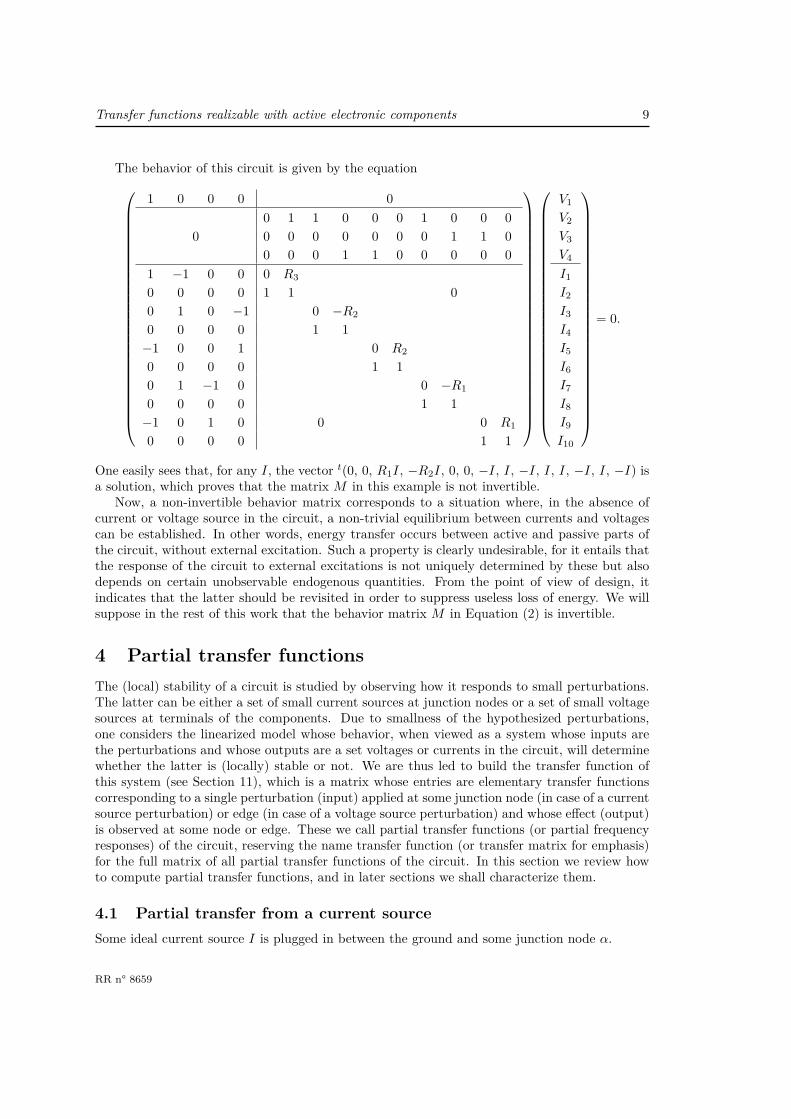
The behavior of this circuit is given by the equation
1 0 0 0 00 1 1 0 0 0 1 0 0 0
0 0 0 0 0 0 0 0 1 1 00 0 0 1 1 0 0 0 0 0
1 −1 0 0 0 R3
0 0 0 0 1 1 00 1 0 −1 0 −R2
0 0 0 0 1 1−1 0 0 1 0 R2
0 0 0 0 1 10 1 −1 0 0 −R1
0 0 0 0 1 1−1 0 1 0 0 0 R1
0 0 0 0 1 1
V1
V2
V3
V4
I1
I2
I3
I4
I5
I6
I7
I8
I9
I10
= 0.
One easily sees that, for any I, the vector t(0, 0, R1I, −R2I, 0, 0, −I, I, −I, I, I, −I, I, −I) isa solution, which proves that the matrix M in this example is not invertible.
Now, a non-invertible behavior matrix corresponds to a situation where, in the absence ofcurrent or voltage source in the circuit, a non-trivial equilibrium between currents and voltagescan be established. In other words, energy transfer occurs between active and passive parts ofthe circuit, without external excitation. Such a property is clearly undesirable, for it entails thatthe response of the circuit to external excitations is not uniquely determined by these but alsodepends on certain unobservable endogenous quantities. From the point of view of design, itindicates that the latter should be revisited in order to suppress useless loss of energy. We willsuppose in the rest of this work that the behavior matrix M in Equation (2) is invertible.
4 Partial transfer functionsThe (local) stability of a circuit is studied by observing how it responds to small perturbations.The latter can be either a set of small current sources at junction nodes or a set of small voltagesources at terminals of the components. Due to smallness of the hypothesized perturbations,one considers the linearized model whose behavior, when viewed as a system whose inputs arethe perturbations and whose outputs are a set voltages or currents in the circuit, will determinewhether the latter is (locally) stable or not. We are thus led to build the transfer function ofthis system (see Section 11), which is a matrix whose entries are elementary transfer functionscorresponding to a single perturbation (input) applied at some junction node (in case of a currentsource perturbation) or edge (in case of a voltage source perturbation) and whose effect (output)is observed at some node or edge. These we call partial transfer functions (or partial frequencyresponses) of the circuit, reserving the name transfer function (or transfer matrix for emphasis)for the full matrix of all partial transfer functions of the circuit. In this section we review howto compute partial transfer functions, and in later sections we shall characterize them.
4.1 Partial transfer from a current sourceSome ideal current source I is plugged in between the ground and some junction node α.
RR n° 8659
10 L. Baratchart, S. Chevillard & F. Seyfert
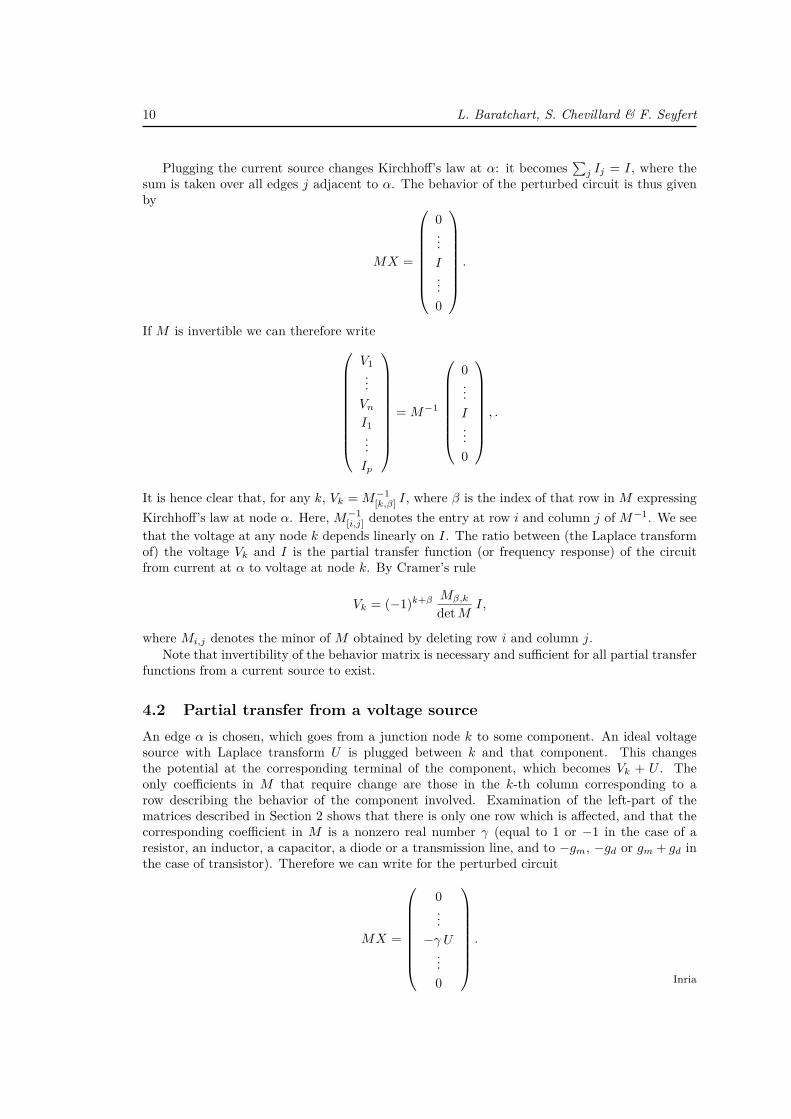
Plugging the current source changes Kirchhoff’s law at α: it becomes∑j Ij = I, where the
sum is taken over all edges j adjacent to α. The behavior of the perturbed circuit is thus givenby
MX =
0...I...0
.
If M is invertible we can therefore write
V1...Vn
I1...Ip
= M−1
0...I...0
, .
It is hence clear that, for any k, Vk = M−1[k,β] I, where β is the index of that row in M expressing
Kirchhoff’s law at node α. Here, M−1[i,j] denotes the entry at row i and column j of M−1. We see
that the voltage at any node k depends linearly on I. The ratio between (the Laplace transformof) the voltage Vk and I is the partial transfer function (or frequency response) of the circuitfrom current at α to voltage at node k. By Cramer’s rule
Vk = (−1)k+β Mβ,k
detM I,
where Mi,j denotes the minor of M obtained by deleting row i and column j.Note that invertibility of the behavior matrix is necessary and sufficient for all partial transfer
functions from a current source to exist.
4.2 Partial transfer from a voltage sourceAn edge α is chosen, which goes from a junction node k to some component. An ideal voltagesource with Laplace transform U is plugged between k and that component. This changesthe potential at the corresponding terminal of the component, which becomes Vk + U . Theonly coefficients in M that require change are those in the k-th column corresponding to arow describing the behavior of the component involved. Examination of the left-part of thematrices described in Section 2 shows that there is only one row which is affected, and that thecorresponding coefficient in M is a nonzero real number γ (equal to 1 or −1 in the case of aresistor, an inductor, a capacitor, a diode or a transmission line, and to −gm, −gd or gm + gd inthe case of transistor). Therefore we can write for the perturbed circuit
MX =
0...
−γ U...0
.
Inria
Transfer functions realizable with active electronic components 11
Denoting with β the index of the row where −γU lies in the above equation, we get using thesame argument as before that, if matrix M is invertible, then
Ir = (−1)r+β Mβ,r
detM (−γ)U, for any r ∈ 1, . . . , p.
The ratio Ir/U is the frequency response at edge r of the circuit to the voltage source U , and againinvertibility of the behavior matrix is necessary and sufficient for all partial transfer functionsfrom a voltage source to exist.
Altogether, we see that the partial transfer function obtained by using a voltage source is ofthe same form as the partial transfer function obtained using a current source. In the rest of thiswork, without loss of generality, we only deal with the latter, that is, we favor transfer functionsof impedance type.
5 R-L-C circuits with negative resistorsAs a first step towards our main results, we describe in this section the structure of partialtransfer functions of circuits that have no transmission line nor transistor in their components.Namely, each partial frequency response of a circuit made of positive resistors, negative resistors,along with standard (i.e. positive) capacitors and inductors, belongs to the field R(s) of rationalfunctions in the variable s with real coefficients, and conversely any f ∈ R(s) can be realized asa partial frequency response of such a circuit. Moreover, we will see (cf. Remark 2 at the endof the present section) that the result still holds if transistors are added to the list of admissiblecomponents.
The above statement is essentially equivalent to a classical property of impedance (rather thanpartial transfer functions) of networks comprising positive resistors, negative resistors, capacitorsand inductors [4]. The latter is formally stated as Theorem 1 in Section 5.2 to come.
Note that the converse part of the statement is concerned with a single partial transferfunction, and says nothing about synthesizing an arbitrary rational matrix as the transfer matrixof a circuit made of resistors of arbitrary sign, capacitors and inductors. Whether this is possibleor not is still an open issue, see [4] where transformers and gyrators are added to the set ofadmissible elements in order to answer the question in the positive.
We now discuss the proof. The fact that each partial frequency response belongs to R(s) isobvious from the previous section, for this frequency response has the form αMβ,k/det(M) withα ∈ R, and M as in equation (2). Besides, since the circuit does not contain transmission lines,all elements of M belong to R(s), thus also Mβ,k/ det(M) ∈ R(s).
The converse part is a little harder, and can be established along the classical lines of Fostersynthesis [3, thm. 5.2.1] by relaxing sign conditions therein, see also [4]. Below, we give a differentproof which lends itself better to generalization when we consider circuits with transmission lines,as will be the case in a forthcoming section.
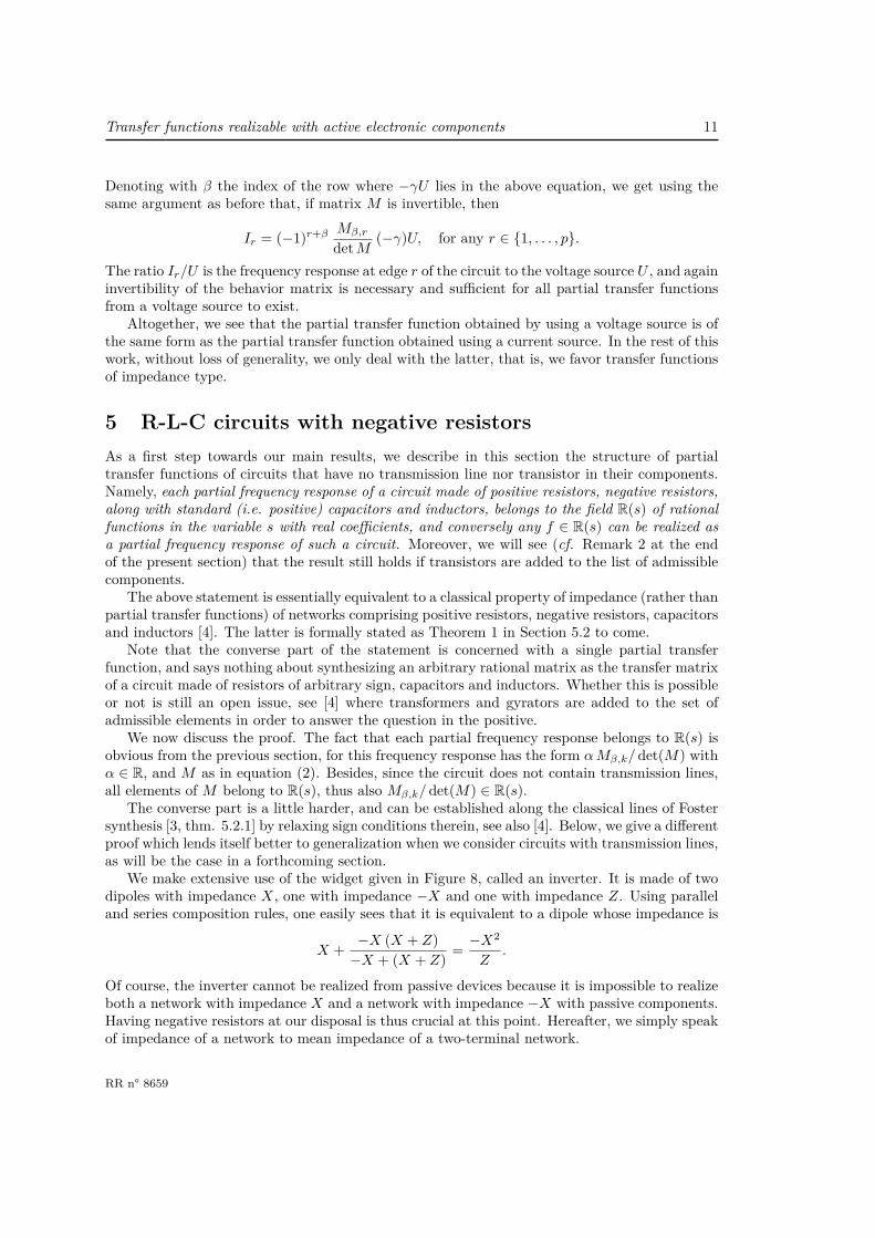
We make extensive use of the widget given in Figure 8, called an inverter. It is made of twodipoles with impedance X, one with impedance −X and one with impedance Z. Using paralleland series composition rules, one easily sees that it is equivalent to a dipole whose impedance is
X + −X (X + Z)−X + (X + Z) = −X
2
Z.
Of course, the inverter cannot be realized from passive devices because it is impossible to realizeboth a network with impedance X and a network with impedance −X with passive components.Having negative resistors at our disposal is thus crucial at this point. Hereafter, we simply speakof impedance of a network to mean impedance of a two-terminal network.
RR n° 8659
12 L. Baratchart, S. Chevillard & F. Seyfert
Figure 8: The inverter network
5.1 What the inverter makes possibleLemma 1. If negative resistors are allowed, and if one has a network with impedance x, it ispossible to build a network with impedance −1/x.
Proof. The inverter of Figure 8 can actually be realized with X = 1 and −X = 1 since wehave negative resistors. Using the network with impedance x for Z, we obtain a network withequivalent impedance −1/Z = −1/x.
Corollary 1. Having positive and negative resistors, along with standard capacitors and induc-tors allows one to emulate negative capacitors and inductors.
Proof. Applying Lemma 1 to a capacitor of capacitance α (i.e. x = 1/(α s)) gives us a negativeinductor of inductance −α. Conversely, applying the lemma to an inductor of inductance α (i.e.x = α s) gives us a negative capacitor of capacitance −α.
Lemma 2. If negative resistors are allowed and if one has an electrical network with impedancex and another one with impedance −x, it is possible to build a network with impedance ±x2.
Proof. We use the inverter again, this time with X = x. This is possible because we can actuallybuild a network with impedance −X. For Z, we can choose as a resistor of resistance ±1(since negative resistors are allowed). We hence obtain a network with equivalent impedance−X2/± 1 = ±x2.
Lemma 3. If negative resistors are allowed and if one has electrical networks with impedancesx, −x, y and −y, it is possible to build a network with impedance ±xy.
Proof. Composing networks for x and y (respectively −x and −y) in series, we get a networkof impedance x + y (respectively −(x + y)). Using Lemma 2, we get circuits with impedances±(x+ y)2, ±x2 and ±y2.
Now, composing in series (x+ y)2, −x2 and −y2, we get a network of equivalent impedance(x+ y)2 + (−x2) + (−y2) = 2xy. The same way, we also get a circuit with impedance x2 + y2 +(−(x+ y)2) = −2xy.
To sum up, we just proved that, having networks with impedances ±x and ±y, one can buildnetworks with impedance ±2xy. Applying this result to ±2xy and a resistor of resistance ±1/4,we get a network with impedance ±xy.
5.2 Frequency response of RLC circuits with negative resistorsTheorem 1. Let P (s)/Q(s) be an arbitrary rational function with real coefficients. Using positiveand negative resistors, capacitors and inductors, it is possible to build a network with impedanceP (s)/Q(s).
Inria

Transfer functions realizable with active electronic components 13
Proof. Using Corollary 1 together with Lemma 3, we see by an elementary induction that wecan build networks with impedances ±αsk for any k ∈ Z. Composing them in series allows usto realize ±P (s) and ±Q(s). Now, using Lemma 1, we can realize ±1/Q(s), and finally, usingLemma 3 again, we get ±P (s)/Q(s).
Let finally P (s) and Q(s) be two polynomials such that 0 6≡ Q 6= P . To establish the resultannounced at the beginning of this section, it remains to observe in view of Theorem 1 that thecircuit shown in Figure 9, where we set R(s) = P (s)/Q(s), is realizable with positive and negativeresistors, inductors, capacitors. Indeed, it consists of a series of two elements with impedance1 and R(s) respectively, with both ports connected to the mass. Now, one easily checks thatthe partial frequency response to a current source plugged at the junction node with output thevoltage at that node is exactly P (s)/Q(s). This achieves the proof.
Figure 9: A circuit with partial frequency response R(s)
Remark 2. Circuits made of positive and negative resistors, capacitors, inductors and linearizedtransistors have exactly the same class of partial frequency responses as those without transistors.Indeed, elements in the matrix describing the behavior of transistors (see Figure 4) also belongto R(s), so the frequency response of circuits with transistors in turn lies in R(s). Since allfunctions from R(s) are already realizable without transistors, this remains a fortiori true whentransistors are allowed.
6 Circuits with transmission linesBelow, we generalize the result of the previous section to the case where circuits consist of allelements listed in Section 2. More precisely, let E be the smallest field containing R(s) as wellas all functions of the form γ(s) sinh(γ(s)) and cosh(γ(s)), where γ(s) =
√(a+ bs)(c+ ds) for
some real numbers a, b, c, d ≥ 0. The determination of the square root involved in the expressionfor γ is irrelevant: choosing a determination or its negative defines the same functions becausecosh is even and sinh is odd. Another way of defining E is, e.g.,
E = (f1 + · · ·+ fn)/(g1 + · · ·+ gm), with f1, . . . , fn, g1, . . . , gm ∈ A where
A =α sk
n∏i=1
γi(s) sinh(γi(s))m∏
i=n+1cosh(γi(s))
α∈R, k∈N,γi(s)=
√(ai+bis)(ci+dis)
where ai, bi, ci, di≥0
.(3)
The main result of this section is that the class of functions realizable as partial transfer functionsof circuits made of elements listed in Section 2, namely positive and negative resistors, capacitors,inductors, linearized transistors and transmission lines, is exactly E .
We follow the same approach as in the previous section. Again, proving that each partialfrequency response belongs to E is very easy: all entries of the matrix M given in Equation (2)belong to E , which is a field, thus any partial frequency response (which is proportional to theratio of a minor of M and its determinant) also belongs to E .
RR n° 8659
14 L. Baratchart, S. Chevillard & F. Seyfert
We now show the converse. For this, we use a trick: we only consider networks with oneavailable terminal, for which a relation of the form V = Z I is satisfied, where V is the potentialof the terminal and I is the current entering the network through the terminal. We call such anetwork a one-port circuit and we call Z the impedance of the circuit.
Figure 10: Representation of a one-port circuit
Of course such circuits form a strict, and in fact very particular subset of all circuits one canbuilt from positive or negative resistors, inductors, capacitors and transmission lines. One couldthink a priori that partial frequency responses realizable in this way are only a small subset ofall partial frequency responses arising from more general topologies. As we will see this is notthe case, as all functions of E can be realized as impedances of one-port circuits already. Now, ifR(s) is an element of E , so is R(s)/(1−R(s)), and we can use again the the circuit of Figure 9.Indeed, it can be synthesized with a one-port circuit of impedance R(s)/(1−R(s)) and a resistorof resistance 1. One easily checks that the partial frequency response obtained by plugging acurrent source at the junction node and looking at the voltage at that same node is again R(s).
6.1 Using transmission lines as one-port circuitsThe reason why we limit our study to one-port circuits is the following. Whereas dipoles are easyto compose in series or parallel and this composition results in nice algebraic combinations oftheir impedance functions, it is not so for transmission lines. Their behavior, recalled in Figure 2,cannot be reduced to a single scalar relation, and one fundamentally needs two linear relationsto express it. Thus, when composing lines with other elements in a circuit, one is led to multiply2× 2 matrices from which it is not easy to keep track of the algebraic structure of the resultingelements.
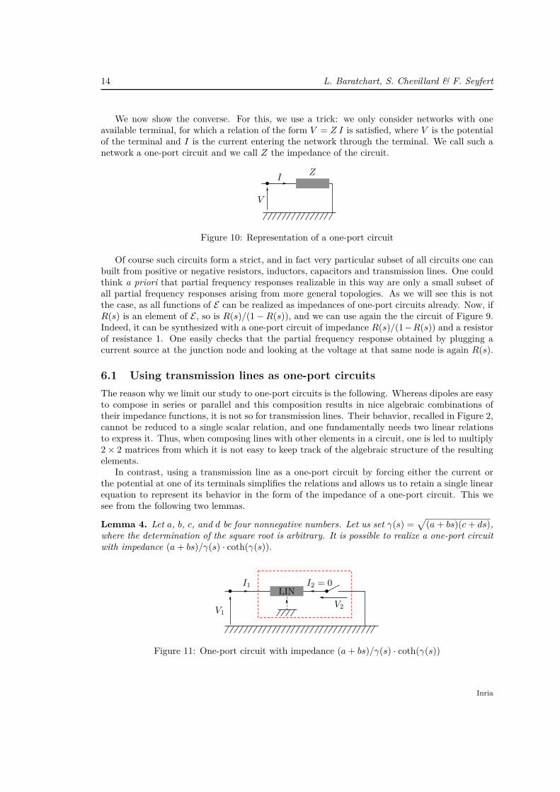
In contrast, using a transmission line as a one-port circuit by forcing either the current orthe potential at one of its terminals simplifies the relations and allows us to retain a single linearequation to represent its behavior in the form of the impedance of a one-port circuit. This wesee from the following two lemmas.
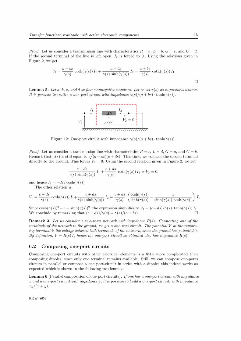
Lemma 4. Let a, b, c, and d be four nonnegative numbers. Let us set γ(s) =√
(a+ bs)(c+ ds),where the determination of the square root is arbitrary. It is possible to realize a one-port circuitwith impedance (a+ bs)/γ(s) · coth(γ(s)).
Figure 11: One-port circuit with impedance (a+ bs)/γ(s) · coth(γ(s))
Inria
Transfer functions realizable with active electronic components 15
Proof. Let us consider a transmission line with characteristics R = a, L = b, G = c, and C = d.If the second terminal of the line is left open, I2 is forced to 0. Using the relations given inFigure 2, we get
V1 = a+ bs
γ(s) coth(γ(s)) I1 + a+ bs
γ(s) sinh(γ(s)) I2 = a+ bs
γ(s) coth(γ(s)) I1
Lemma 5. Let a, b, c, and d be four nonnegative numbers. Let us set γ(s) as in previous lemma.It is possible to realize a one-port circuit with impedance γ(s)/(a+ bs) · tanh(γ(s)).
Figure 12: One-port circuit with impedance γ(s)/(a+ bs) · tanh(γ(s)).
Proof. Let us consider a transmission line with characteristics R = c, L = d, G = a, and C = b.Remark that γ(s) is still equal to
√(a+ bs)(c+ ds). This time, we connect the second terminal
directly to the ground. This forces V2 = 0. Using the second relation given in Figure 2, we get
c+ ds
γ(s) sinh(γ(s)) I1 + c+ ds
γ(s) coth(γ(s)) I2 = V2 = 0,
and hence I2 = −I1/ cosh(γ(s)).The other relation is
V1 = c+ ds
γ(s) coth(γ(s)) I1+ c+ ds
γ(s) sinh(γ(s)) I2 = c+ ds
γ(s)
(cosh(γ(s))sinh(γ(s)) −
1sinh(γ(s)) cosh(γ(s))
)I1.
Since cosh(γ(s))2−1 = sinh(γ(s))2, the expression simplifies to V1 = (c+ds)/γ(s) ·tanh(γ(s)) I1.We conclude by remarking that (c+ ds)/γ(s) = γ(s)/(a+ bs).
Remark 3. Let us consider a two-ports network with impedance R(s). Connecting one of theterminals of the network to the ground, we get a one-port circuit. The potential V at the remain-ing terminal is the voltage between both terminals of the network, since the ground has potential 0.By definition, V = R(s) I, hence the one-port circuit so obtained also has impedance R(s).
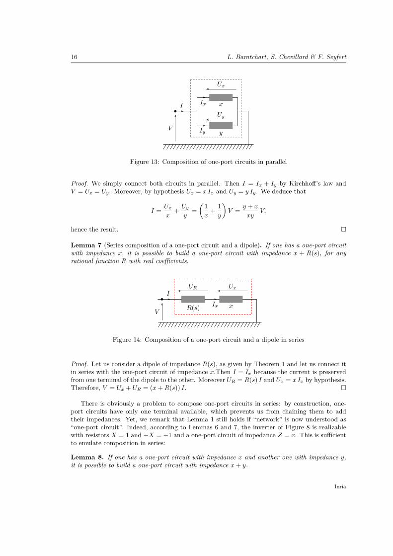
6.2 Composing one-port circuitsComposing one-port circuits with other electrical elements is a little more complicated thancomposing dipoles, since only one terminal remains available. Still, we can compose one-portscircuits in parallel or compose a one port-circuit in series with a dipole: this indeed works asexpected which is shown in the following two lemmas.
Lemma 6 (Parallel composition of one-port circuits). If one has a one-port circuit with impedancex and a one-port circuit with impedance y, it is possible to build a one-port circuit, with impedancexy/(x+ y).
RR n° 8659
16 L. Baratchart, S. Chevillard & F. Seyfert
Figure 13: Composition of one-port circuits in parallel
Proof. We simply connect both circuits in parallel. Then I = Ix + Iy by Kirchhoff’s law andV = Ux = Uy. Moreover, by hypothesis Ux = x Ix and Uy = y Iy. We deduce that
I = Uxx
+ Uyy
=(
1x
+ 1y
)V = y + x
xyV,
hence the result.
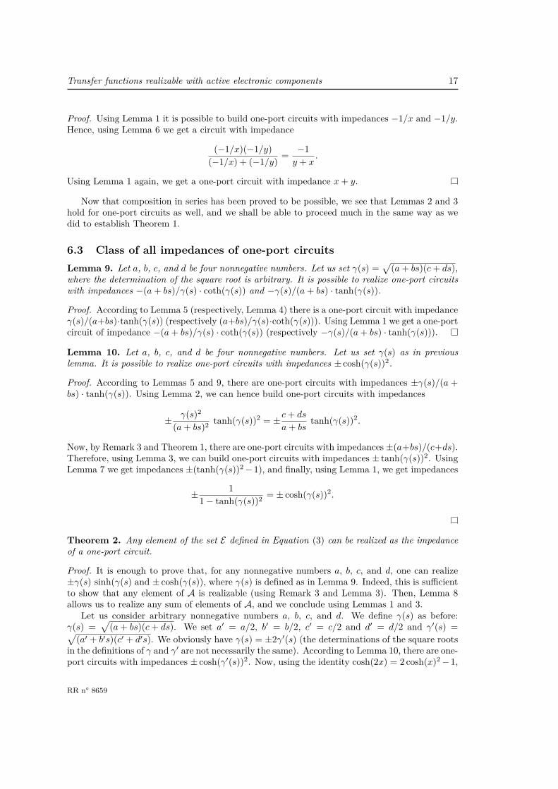
Lemma 7 (Series composition of a one-port circuit and a dipole). If one has a one-port circuitwith impedance x, it is possible to build a one-port circuit with impedance x + R(s), for anyrational function R with real coefficients.
Figure 14: Composition of a one-port circuit and a dipole in series
Proof. Let us consider a dipole of impedance R(s), as given by Theorem 1 and let us connect itin series with the one-port circuit of impedance x.Then I = Ix because the current is preservedfrom one terminal of the dipole to the other. Moreover UR = R(s) I and Ux = x Ix by hypothesis.Therefore, V = Ux + UR = (x+R(s)) I.
There is obviously a problem to compose one-port circuits in series: by construction, one-port circuits have only one terminal available, which prevents us from chaining them to addtheir impedances. Yet, we remark that Lemma 1 still holds if “network” is now understood as“one-port circuit”. Indeed, according to Lemmas 6 and 7, the inverter of Figure 8 is realizablewith resistors X = 1 and −X = −1 and a one-port circuit of impedance Z = x. This is sufficientto emulate composition in series:
Lemma 8. If one has a one-port circuit with impedance x and another one with impedance y,it is possible to build a one-port circuit with impedance x+ y.
Inria
Transfer functions realizable with active electronic components 17
Proof. Using Lemma 1 it is possible to build one-port circuits with impedances −1/x and −1/y.Hence, using Lemma 6 we get a circuit with impedance
(−1/x)(−1/y)(−1/x) + (−1/y) = −1
y + x.
Using Lemma 1 again, we get a one-port circuit with impedance x+ y.
Now that composition in series has been proved to be possible, we see that Lemmas 2 and 3hold for one-port circuits as well, and we shall be able to proceed much in the same way as wedid to establish Theorem 1.
6.3 Class of all impedances of one-port circuitsLemma 9. Let a, b, c, and d be four nonnegative numbers. Let us set γ(s) =
√(a+ bs)(c+ ds),
where the determination of the square root is arbitrary. It is possible to realize one-port circuitswith impedances −(a+ bs)/γ(s) · coth(γ(s)) and −γ(s)/(a+ bs) · tanh(γ(s)).
Proof. According to Lemma 5 (respectively, Lemma 4) there is a one-port circuit with impedanceγ(s)/(a+bs)·tanh(γ(s)) (respectively (a+bs)/γ(s)·coth(γ(s))). Using Lemma 1 we get a one-portcircuit of impedance −(a+ bs)/γ(s) · coth(γ(s)) (respectively −γ(s)/(a+ bs) · tanh(γ(s))).
Lemma 10. Let a, b, c, and d be four nonnegative numbers. Let us set γ(s) as in previouslemma. It is possible to realize one-port circuits with impedances ± cosh(γ(s))2.
Proof. According to Lemmas 5 and 9, there are one-port circuits with impedances ±γ(s)/(a +bs) · tanh(γ(s)). Using Lemma 2, we can hence build one-port circuits with impedances
± γ(s)2
(a+ bs)2 tanh(γ(s))2 = ±c+ ds
a+ bstanh(γ(s))2.
Now, by Remark 3 and Theorem 1, there are one-port circuits with impedances ±(a+bs)/(c+ds).Therefore, using Lemma 3, we can build one-port circuits with impedances ± tanh(γ(s))2. UsingLemma 7 we get impedances ±(tanh(γ(s))2−1), and finally, using Lemma 1, we get impedances
± 11− tanh(γ(s))2 = ± cosh(γ(s))2.
Theorem 2. Any element of the set E defined in Equation (3) can be realized as the impedanceof a one-port circuit.
Proof. It is enough to prove that, for any nonnegative numbers a, b, c, and d, one can realize±γ(s) sinh(γ(s) and ± cosh(γ(s)), where γ(s) is defined as in Lemma 9. Indeed, this is sufficientto show that any element of A is realizable (using Remark 3 and Lemma 3). Then, Lemma 8allows us to realize any sum of elements of A, and we conclude using Lemmas 1 and 3.
Let us consider arbitrary nonnegative numbers a, b, c, and d. We define γ(s) as before:γ(s) =
√(a+ bs)(c+ ds). We set a′ = a/2, b′ = b/2, c′ = c/2 and d′ = d/2 and γ′(s) =√
(a′ + b′s)(c′ + d′s). We obviously have γ(s) = ±2γ′(s) (the determinations of the square rootsin the definitions of γ and γ′ are not necessarily the same). According to Lemma 10, there are one-port circuits with impedances ± cosh(γ′(s))2. Now, using the identity cosh(2x) = 2 cosh(x)2−1,
RR n° 8659
18 L. Baratchart, S. Chevillard & F. Seyfert
we see that cosh(γ′(s))2 = 12 cosh(±γ(s))+ 1
2 . Using Lemma 7, and since cosh is an even function,we get impedances ± 1
2 cosh(γ(s)), and by addition we can get rid of the factor 1/2.Furthermore, since we have impedances ± 1
2 cosh(γ(s)) and ± γ(s)a+bs tanh(γ(s)), we get
± γ(s)2(a+ bs) sinh(γ(s))
by Lemma 3. Using Remark 3 and Theorem 1, there are one-port circuits with impedances±2(a+bs). Thus, by Lemma 3 again, we can build one-port circuit with impedance ±γ(s) sinh γ(s), asdesired.
Remark 4. Note that each element of E is a meromorphic function on C, for branchpoints like−ai/bi, and −ci/di in Equation (3) ( cf. page 13), which are a priori of order 2, are in factartificial by evenness of s 7→ γ(s) sinh γ(s) and s 7→ cosh γ(s).
7 Notion of stabilityIt is natural to say that a circuit is (locally) stable with respect to small current perturbationsif every partial transfer function is stable, and similarly for voltages. In other words, stabilityshould refer to the collection of all partial transfer functions (i.e. to the transfer matrix). Inpractice, however, the computational complexity involved with plugging current sources at everyjunction node (or voltage sources at every edge) and checking their effect on each current orvoltage in the circuit often lies beyond computational and experimental capabilities. Typically,one is content with checking stability on a couple of well-chosen partial transfer functions. Wedo not lean on the issue of how to pick those, but we shall discuss stability of a single partialtransfer function from a current source at a node to a voltage at a node.
The standard definition of stability for a linear dynamical system is that it maps input signalsof finite energy (i.e. of bounded L2-norm, both in time and frequency domain since the Fouriertransform is an isometry) to output signals of finite energy. This type of stability is denoted asBIBO, that stands for Bounded Input Bounded Output. Equivalently, a linear dynamical systemis stable if its transfer function belongs to the Hardy space H∞, i.e. if it is holomorphic andbounded in the right half-plane (see Section 11). This definition is not satisfactory here, forit would term unstable such simple passive components as pure inductors (i.e. Z = Ls), purecapacitors (i.e. Z = 1/(Cs)), or ideal transmission lines (those for which when R = G = 0 inSection 2.2). To circumvent this difficulty, we first argue that no current source is ever ideal: italways has internal resistance, that in the near to ideal case can be considered as a very largeresistor connecting the ground to the node where we plug the current source. Next, we take a hintfrom scattering theory: if Z is the partial transfer function and R > 0 is the load of the currentsource, then (R − Z)/(R + Z) is the transfer-function from the incoming (maximum available)power wave to the reflected power wave. In other words, |(R−Z(iω))/(R+Z(iω))|2 is that fractionof the maximum power that the current source can supply to the system which bounces back, atfrequency ω, and if I is the intensity of the current then (1− |(R− Z(iω))/(R+ Z(iω)|2)RI2/4is the power actually dissipated by Z (see [8]).
When the circuit is passive, then <Z ≥ 0 hence the fraction of reflected power is less than 1,that is to say (R− Z)/(R+ Z) lies in H∞ and its supremum norm is at most 1. This indicatesthat the system does not generate energy. When the circuit is active, which is the case when itcontains diodes or transistors, the reflected fraction of the incoming power can be greater than1 at some or all frequencies, which means that the system generates energy at those frequencies.For instance, an amplifier is expected to magnify the signal it receives. Of course, the necessary
Inria
Transfer functions realizable with active electronic components 19
power supply to do this has to come from an external source, used to generate voltage at terminalsof the primary circuits of diodes and transistors. Thus, even if it has norm greater than unity,(R− Z)/(R+ Z) should still lie in H∞ to prevent instabilities, namely, working rates for whichthe energy demand to these primary circuits becomes infinite. In view of this, it seems natural tosay that Z is stable if (R−Z)/(R+Z) ∈ H∞. However, we do not want the degree of stability ofZ to depend on the actual value of the load, which leads us to the make the following definitionwhich we could not locate in the literature.
Definition 1. Let Z be a partial frequency response of a circuit. We say that Z is stable if thereexists R0 > 0 and M > 0 such that
∀R > R0,R− ZR+ Z
∈ H∞ and∥∥∥∥R− ZR+ Z
∥∥∥∥H∞≤M. (4)
The same definition applies to the impedance of a two-ports.
In other words, our definition states that a circuit is stable, if in terms of power waves it isof BIBO type, and this for all near to perfect feeding current sources (i.e R ≥ R0). Definition 1of stability is more general than the BIBO condition on Z:
Lemma 11. If Z ∈ H∞ (i.e. if Z is stable in the usual sense), then Z is also stable in the senseof Definition 1.
Proof. Since Z ∈ H∞ it holds that |Z(s)| < M for some M and all s with <s > 0. If we setR0 = M + 1, then |Z(s) + R| ≥ 1 for all R ≥ R0, so that |(R − Z(s))/(R + Z(s))| is boundedabove by R+M , implying that it lies in H∞.
Note that the converse of Lemma 11 is not true, e.g. ideal inductors and capacitors becomesstable with Definition (4), although they are not themselves in H∞.
As pointed out in Section 5, circuits made of positive resistors, negative resistors, capacitorsand inductors have rational partial transfer functions, in which case Definition 1 simply saysthat the rational function (R − Z)/(R + Z) has no pole in the closed right half-plane for all Rlarge enough, including at infinity. In fact, this function cannot have poles at infinity anyway(i.e. it is proper), because either Z has a pole there and then (R−Z)/(R+Z)(∞) = −1, or elseZ(∞) = a ∈ C in which case (R−Z)/(R+Z) has finite value at infinity for each R > |a|. Thus,for such circuits, stability simply means that (R− Z)/(R+ Z) has no no pole at finite distancein the closed right half-plane, whenever R is large enough. This familiar criterion for stabilityno longer holds when lines are present in the circuit, as follows from the example below. Set
f(s) = s tanh(s)− 1s+ 1 and Z(s) = 2f(s)
f(s) + 2 . (5)
We will show that for all R large enough, s 7→ (R − Z(s))/(R + Z(s)) is defined and finite on<s ≥ 0 but does not belong to H∞. This will provide us with an example of a transfer functionwhich is unstable in the sense of Definition 1, yet has no poles in the right half-plane. We proceedvia the following steps.
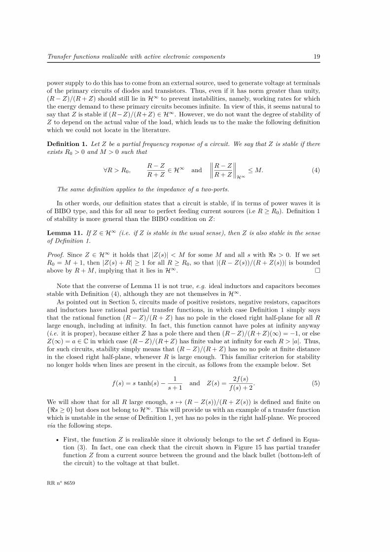
• First, the function Z is realizable since it obviously belongs to the set E defined in Equa-tion (3). In fact, one can check that the circuit shown in Figure 15 has partial transferfunction Z from a current source between the ground and the black bullet (bottom-left ofthe circuit) to the voltage at that bullet.
RR n° 8659
20 L. Baratchart, S. Chevillard & F. Seyfert
Figure 15: Realization of a function that is unstable, though it has no pole in the right half-plane.
• Next, we remark that the equation f(s) = −a where a ∈ [1, +∞[ has no solution s in theright half-plane. Indeed,
f(s) = −a⇐⇒ tanh(s) + 1s+ 1 = 1− a
s.
We observe that tanh(s) + 1/(s + 1) has a positive real part whenever <(s) ≥ 0 though(1− a)/s has a non-positive real part. Thus they cannot be equal.
• Consequently, for all R > 2, the function (R − Z)/(R + Z) is finite at every point of theclosed right half-plane. Indeed, since
R− ZR+ Z
= R− 2R+ 2 ·
f(s) + 2RR−2
f(s) + 2RR+2
, (6)
it follows from the previous item that the denominator cannot vanish for <s ≥ 0 and,though f may have poles there, the function (R−Z)/(R+Z) is analytically continued atthem with value (R− 2)/(R+ 2).
• To recap, we just showed that for any R > 2 the function (R−Z)/(R+Z) is holomorphicin <s ≥ 0. Still, we claim that it does not belong to H∞. Indeed, put for simplicityα = 2R/(R+ 2) and consider the sequence of points sk = i (kπ + α/(kπ)). Then
sk tanh(sk) = −(kπ + α
kπ
)tan
( αkπ
)= −α+
(1k
),
Inria
Transfer functions realizable with active electronic components 21
from which we deduce the following identities:f(sk) + α = − 1
sk + 1 + (
1k
)= − 1
ikπ + (
1k
)R−2R+2f(sk) + α =
(1− R−2
R+2
)α+ (1) = 8R/(R+ 2)2 + (1) .
From Equation (6), we obtain
R− ZR+ Z
=R−2R+2f + α
f + α,
and so, its value at point sk is−8ikπR/(R+2)2+(k). Hence, we did exhibit (for any R > 2)a sequence of points on the imaginary axis along which (R − Z)/(R + Z) is unbounded.This shows it cannot lie in H∞ (cf. Section 11).
Remark: (R−Z)/(R+Z) does not belong either to the space H2 nor to any Hp (see definitionin Section 11). To see this, remark that
f(s) = s2 tanh(s) + s tanh(s)− 1s+ 1 ,
hence, setting β = (R− 2)/(R+ 2), we have
R− ZR+ Z
= βf(s) + α
f(s) + α= β(s2 tanh(s) + s tanh(s)− 1) + α(s+ 1)
s2 tanh(s) + s tanh(s)− 1 + α (s+ 1) .
Now, setting M = 1/ tanh(s) we can rewrite the previous expression as
R− ZR+ Z
= β(1 + 1/s−M/s2) + αM/s+ αM/s2
1 + (1 + αM)/s+ (α− 1)M/s2 .
Whenever R > 2, we have 1 < α < 2 and 0 < β < 1. Let us consider s = i (kπ+ t) where k is aninteger such that |k|π ≥ 6 + 4/β and t ∈ [π/4, 3π/4]. Then, |s| ≥ 6 + 4/β and |M | ≤ 1. Fromthis we deduce that∣∣∣∣R− ZR+ Z
∣∣∣∣ ≥ β(
1− 16+4/β −
1(6+4/β)2
)− 2
6+4/β −2
(6+4/β)2
1 + 36+4/β + 1
(6+4/β)2
= 29β2 + 30β + 855β2 + 60β + 16 β ≥
β
2 .
In conclusion, we obtained a positive lower bound of |(R− Z)/(R+ Z)| valid on any interval ofthe form [iπ(k + 1/4), iπ(k + 3/4)] (k ∈ Z large enough): this shows that (R−Z)/(R+Z) doesnot belong to Lp of the imaginary axis, so it belongs to no Hardy space.
A pending issue. The example just constructed has pathological behavior because it has asequence of poles located in the open left half-plane but asymptotically close to the imaginaryaxis at large frequencies. One may ask if a partial transfer function can be unstable (with respectto Definition 1) when the set of poles is at strictly positive distance from the axis. Symmetrically,if a partial transfer function has poles arbitrarily close to the axis, is it necessarily unstable? Itis not known to the authors whether stability, in the sense of Definition 1, can be describedsolely in terms of poles of the partial transfer function. In this connection, we mention that thebehavior of poles of rational functions in the variable s and in real powers of exp(s) (the subset
RR n° 8659
22 L. Baratchart, S. Chevillard & F. Seyfert
of E attainable with lossless lines, i.e. those for which a = c = 0) is well-known [10]: they areasymptotic either to vertical lines or to curves separating exponentially fast from the imaginaryaxis. The situation with lossy lines has apparently not attracted much attention, and may bemore complicated.
Until now, we considered linearized diodes as pure negative resistors and linearized transistorsas pure current sources controlled by voltages. Such ideal models are simple and usually leadto good approximation at working frequencies, therefore they are widely used in simulationand design. However, the example of Figure 15 shows that checking stability does not reducethen to verify that poles have strictly negative real part. This somewhat contradicts commonengineering practice, and puts a question mark on the use of ideal linearized models in connectionwith stability.
Actually, ideal models are somewhat unrealistic: even if it does not show at working fre-quencies, no active component has gain at all frequencies for there are always small resistive,capacitive and inductive effects in a physical device. As we will see in the next section, tak-ing them into account restricts considerably the class of transfer functions realizable with suchcircuits.
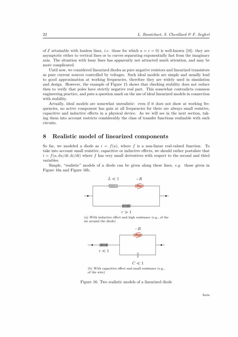
8 Realistic model of linearized componentsSo far, we modeled a diode as i = f(u), where f is a non-linear real-valued function. Totake into account small resistive, capacitive or inductive effects, we should rather postulate thati = f(u,du/dt, di/dt) where f has very small derivatives with respect to the second and thirdvariables.
Simple, “realistic” models of a diode can be given along these lines, e.g. those given inFigure 16a and Figure 16b.
(a) With inductive effect and high resistance (e.g., of theair around the diode)
(b) With capacitive effect and small resistance (e.g.,of the wire)
Figure 16: Two realistic models of a linearized diode
Inria

Transfer functions realizable with active electronic components 23
Of course, physical reality is much more complex and it is pointless to attempt at giving acomplete and accurate model of a linearized diode at all frequencies. Besides, different types ofdiodes would require different descriptions and it would be cumbersome to distinguish betweenthem, while the differences are completely negligible in practice in the range of frequencies wherethe diodes are intended to be use. Instead, we put forward the paradigm that “what happens atvery large frequencies is unimportant beyond passivity”, and we shall use a somewhat abstractdefinition to accommodate various cases occurring in practice.
Definition 2. A realistic linearized diode is a dipole with complex impedance Z having thefollowing characteristics:
• Z(s) is a rational function with real coefficients.
• When |s| < ω0, it holds that Z(s) = −R + ε(s) where ε is a function whose modulus isnegligible compared to other quantities in the circuit.
• When |s| > ω1 and <(s) ≥ 0, we have <(Z(s)) ≥ 0.
In this definition, 0 < ω0 < ω1 as well as R are positive real numbers.
The hypothesis “Z is a rational function with real coefficients” simply states that a realisticnegative resistor may, in principle, be described as a combination of a pure negative resistor andstandard passive linear dipoles. In particular both models proposed in Figure 16 comply withDefinition 2, but many other models would also meet our requirements.
Remark 5. The same argument as in Remark 1 ( cf. page 4) shows that, if V1, V2, I1 and I2denote the potentials and currents at both terminals of a realistic linearized diode, then
V1 I1 + V2 I2 = Z|I1|2 = Z|I2|2.
Therefore, when |s| > ω1 and <(s) ≥ 0, we have that <(V1 I1 + V2 I2) ≥ 0.
Transistors can in turn be modeled in a “realistic” way, to account for the fact that they do notprovide gain at very high frequencies. For instance, the model presented in Figure 17 correspondsto what is called the intrinsic model of the linearized transistor and displays capacitive effectsappearing at the junctions between semiconductors. As in the case of a diode, reality is stillmore complex and involves both inductive and capacitive effects that we do not try to modelsince they are irrelevant to our discussion.
Figure 17: Intrinsic model of a linearized transistor
This leads us to the following definition, in the spirit of Definition 2:
RR n° 8659
24 L. Baratchart, S. Chevillard & F. Seyfert
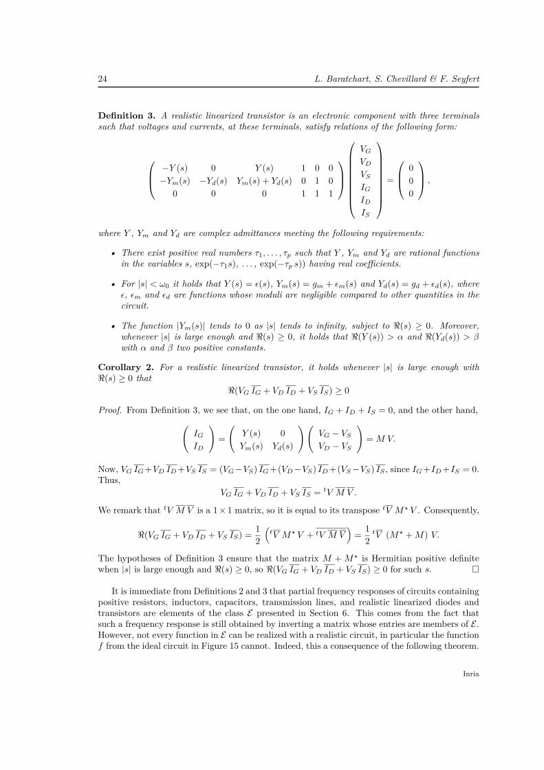
Definition 3. A realistic linearized transistor is an electronic component with three terminalssuch that voltages and currents, at these terminals, satisfy relations of the following form:
−Y (s) 0 Y (s) 1 0 0−Ym(s) −Yd(s) Ym(s) + Yd(s) 0 1 0
0 0 0 1 1 1
VG
VD
VS
IG
ID
IS
=
000
,
where Y , Ym and Yd are complex admittances meeting the following requirements:
• There exist positive real numbers τ1, . . . , τp such that Y , Ym and Yd are rational functionsin the variables s, exp(−τ1s), . . . , exp(−τp s)) having real coefficients.
• For |s| < ω0 it holds that Y (s) = ε(s), Ym(s) = gm + εm(s) and Yd(s) = gd + εd(s), whereε, εm and εd are functions whose moduli are negligible compared to other quantities in thecircuit.
• The function |Ym(s)| tends to 0 as |s| tends to infinity, subject to <(s) ≥ 0. Moreover,whenever |s| is large enough and <(s) ≥ 0, it holds that <(Y (s)) > α and <(Yd(s)) > βwith α and β two positive constants.
Corollary 2. For a realistic linearized transistor, it holds whenever |s| is large enough with<(s) ≥ 0 that
<(VG IG + VD ID + VS IS) ≥ 0
Proof. From Definition 3, we see that, on the one hand, IG + ID + IS = 0, and the other hand,(IG
ID
)=(
Y (s) 0Ym(s) Yd(s)
)(VG − VSVD − VS
)= M V.
Now, VG IG+VD ID+VS IS = (VG−VS) IG+(VD−VS) ID+(VS−VS) IS , since IG+ID+IS = 0.Thus,
VG IG + VD ID + VS IS = tV M V .
We remark that tV M V is a 1×1 matrix, so it is equal to its transpose tV M? V . Consequently,
<(VG IG + VD ID + VS IS) = 12
(tV M? V + tV M V
)= 1
2tV (M? +M) V.
The hypotheses of Definition 3 ensure that the matrix M + M? is Hermitian positive definitewhen |s| is large enough and <(s) ≥ 0, so <(VG IG + VD ID + VS IS) ≥ 0 for such s.
It is immediate from Definitions 2 and 3 that partial frequency responses of circuits containingpositive resistors, inductors, capacitors, transmission lines, and realistic linearized diodes andtransistors are elements of the class E presented in Section 6. This comes from the fact thatsuch a frequency response is still obtained by inverting a matrix whose entries are members of E .However, not every function in E can be realized with a realistic circuit, in particular the functionf from the ideal circuit in Figure 15 cannot. Indeed, this a consequence of the following theorem.
Inria
Transfer functions realizable with active electronic components 25
Theorem 3. Let a circuit consists of resistors, inductors, capacitors, transmission lines andrealistic linearized diodes and transistors (cf. Definitions 2 and 3). Assume as always that thebehavior matrix of the circuit is invertible. To each partial frequency response Z(s) of the circuit,there exists K > 0 such that, whenever <(s) ≥ 0 and |s| ≥ K, we have <(Z(s)) ≥ 0.
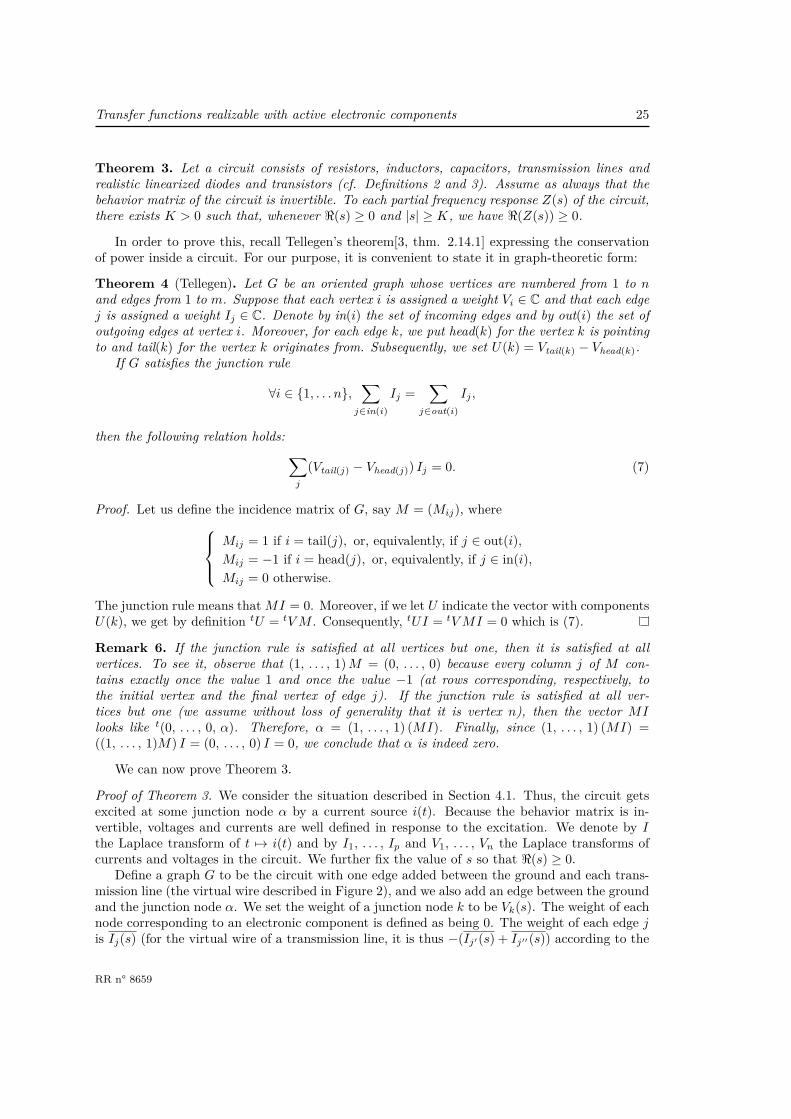
In order to prove this, recall Tellegen’s theorem[3, thm. 2.14.1] expressing the conservationof power inside a circuit. For our purpose, it is convenient to state it in graph-theoretic form:
Theorem 4 (Tellegen). Let G be an oriented graph whose vertices are numbered from 1 to nand edges from 1 to m. Suppose that each vertex i is assigned a weight Vi ∈ C and that each edgej is assigned a weight Ij ∈ C. Denote by in(i) the set of incoming edges and by out(i) the set ofoutgoing edges at vertex i. Moreover, for each edge k, we put head(k) for the vertex k is pointingto and tail(k) for the vertex k originates from. Subsequently, we set U(k) = Vtail(k) − Vhead(k).
If G satisfies the junction rule
∀i ∈ 1, . . . n,∑
j∈in(i)
Ij =∑
j∈out(i)
Ij ,
then the following relation holds:∑j
(Vtail(j) − Vhead(j)) Ij = 0. (7)
Proof. Let us define the incidence matrix of G, say M = (Mij), whereMij = 1 if i = tail(j), or, equivalently, if j ∈ out(i),Mij = −1 if i = head(j), or, equivalently, if j ∈ in(i),Mij = 0 otherwise.
The junction rule means thatMI = 0. Moreover, if we let U indicate the vector with componentsU(k), we get by definition tU = tVM . Consequently, tUI = tVMI = 0 which is (7).
Remark 6. If the junction rule is satisfied at all vertices but one, then it is satisfied at allvertices. To see it, observe that (1, . . . , 1)M = (0, . . . , 0) because every column j of M con-tains exactly once the value 1 and once the value −1 (at rows corresponding, respectively, tothe initial vertex and the final vertex of edge j). If the junction rule is satisfied at all ver-tices but one (we assume without loss of generality that it is vertex n), then the vector MIlooks like t(0, . . . , 0, α). Therefore, α = (1, . . . , 1) (MI). Finally, since (1, . . . , 1) (MI) =((1, . . . , 1)M) I = (0, . . . , 0) I = 0, we conclude that α is indeed zero.
We can now prove Theorem 3.
Proof of Theorem 3. We consider the situation described in Section 4.1. Thus, the circuit getsexcited at some junction node α by a current source i(t). Because the behavior matrix is in-vertible, voltages and currents are well defined in response to the excitation. We denote by Ithe Laplace transform of t 7→ i(t) and by I1, . . . , Ip and V1, . . . , Vn the Laplace transforms ofcurrents and voltages in the circuit. We further fix the value of s so that <(s) ≥ 0.
Define a graph G to be the circuit with one edge added between the ground and each trans-mission line (the virtual wire described in Figure 2), and we also add an edge between the groundand the junction node α. We set the weight of a junction node k to be Vk(s). The weight of eachnode corresponding to an electronic component is defined as being 0. The weight of each edge jis Ij(s) (for the virtual wire of a transmission line, it is thus −(Ij′(s) + Ij′′(s)) according to the
RR n° 8659

26 L. Baratchart, S. Chevillard & F. Seyfert
last line of the matrix in Figure 2). The weight of the edge between the ground and node α isdefined as I(s).
We first observe that G satisfies the junction rule. Indeed, for each vertex of G correspondingto a junction node of the circuit (except maybe the ground), this follows from Kirchhoff’s law; atnodes that are electronic components, this is true by examination of the last line of the behaviormatrix of each component (cf. Section 2). The junction rule is hence satisfied at all verticesof G except maybe for the ground. But from Remark 6, we see that the junction rule is thennecessarily satisfied at all vertices including the ground. We can thus apply Tellegen’s theorem.
By construction, all edges but the one between the ground and node α are oriented from ajunction node to an electronic component. Since the weight of an electronic components is 0,each term (Vtail(j) − Vhead(j)) Ij in Equation (7) becomes Vtail(j)(s) Ij(s) in the present case.Moreover, since the ground has voltage 0, the term corresponding to the edge between theground and node α is (0−Vα(s)) I(s). Since by definition Vα(s) = Z(s) I(s), Tellegen’s theorem,applied to the graph G, gives us∑
j
Vtail(j)(s) Ij(s) = Z(s) |I(s)|2. (8)
Now, since each edge in the circuit is adjacent to exactly one electronic component, we canrewrite the left hand side of (8) as a sum over all electronic components i to obtain∑
i
∑junction node β
adjacent to i
Vβ(s) Iβ→i(s) = Z(s) |I(s)|2,
where Iβ→i(s) denotes the weight of the edge between node β and electronic component i.Applying Remark 1, Remark 5, Corollary 2 or Lemma 12 (cf. Section 10) according whether iis a passive dipole, a realistic linearized diode, a realistic linearized transistor or a transmissionline, we see whenever <(s) ≥ 0 and |s| is large enough that, for each i,
<
∑β
Vβ(s) Iβ→i(s)
≥ 0.
Hence, the left hand side of Equation (8) has positive real part provided that <(s) ≥ 0 and |s|is large enough, and so does Z(s).
Below we draw two important consequences of Theorem 3. They point at a remarkabledifference between the case of ideal linearized elements described in Section 6, and the case ofrealistic linearized elements.
Corollary 3. Let Z be a partial frequency response of a circuit made of transmission lines,resistors, capacitors, inductors, and realistic linearized diodes and transistors. For <(s) ≥ 0 and|s| large enough, it holds for all R ≥ 0 that |(R− Z(s))/(R+ Z(s))| ≤ 1.
Proof. Let K be as in Theorem 3. Then, for |s| > K and <(s) ≥ 0, we have as soon as R ≥ 0that |<(R− Z(s))| ≤ <(R+ Z(s)), and it is otherwise clear that =(R− Z(s)) = −=(R+ Z(s)),hence |R− Z(s)| ≤ |R+ Z(s)|, as desired.
Corollary 4. Assumptions and notations being as in Theorem 3, it holds for each R ≥ 0 thatthe meromorphic function (R−Z)/(R+Z) has finitely many poles in the closed right half plane.
Inria
Transfer functions realizable with active electronic components 27
Proof. From the previous corollary we see that the poles of (R−Z)/(R+Z) in the closed righthalf plane have to lie in a disk of radius K centered at 0. Since (R − Z)/(R + Z) ∈ E , it is ameromorphic function on C by Remark 4. Hence poles cannot accumulate, therefore they arefinite in number.
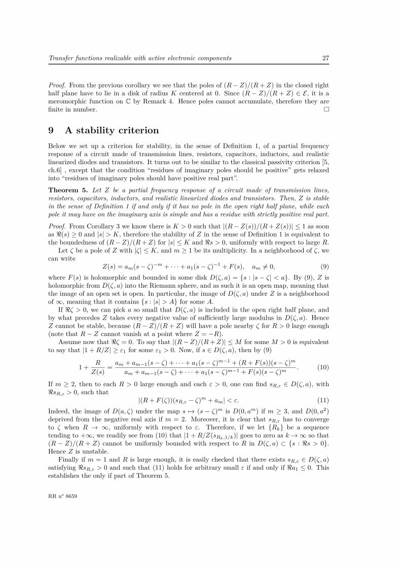
9 A stability criterionBelow we set up a criterion for stability, in the sense of Definition 1, of a partial frequencyresponse of a circuit made of transmission lines, resistors, capacitors, inductors, and realisticlinearized diodes and transistors. It turns out to be similar to the classical passivity criterion [5,ch.6] , except that the condition “residues of imaginary poles should be positive” gets relaxedinto “residues of imaginary poles should have positive real part”.
Theorem 5. Let Z be a partial frequency response of a circuit made of transmission lines,resistors, capacitors, inductors, and realistic linearized diodes and transistors. Then, Z is stablein the sense of Definition 1 if and only if it has no pole in the open right half plane, while eachpole it may have on the imaginary axis is simple and has a residue with strictly positive real part.
Proof. From Corollary 3 we know there is K > 0 such that |(R−Z(s))/(R+Z(s))| ≤ 1 as soonas <(s) ≥ 0 and |s| > K, therefore the stability of Z in the sense of Definition 1 is equivalent tothe boundedness of (R−Z)/(R+Z) for |s| ≤ K and <s > 0, uniformly with respect to large R.
Let ζ be a pole of Z with |ζ| ≤ K, and m ≥ 1 be its multiplicity. In a neighborhood of ζ, wecan write
Z(s) = am(s− ζ)−m + · · ·+ a1(s− ζ)−1 + F (s), am 6= 0, (9)where F (s) is holomorphic and bounded in some disk D(ζ, a) = s : |s − ζ| < a. By (9), Z isholomorphic from D(ζ, a) into the Riemann sphere, and as such it is an open map, meaning thatthe image of an open set is open. In particular, the image of D(ζ, a) under Z is a neighborhoodof ∞, meaning that it contains s : |s| > A for some A.
If <ζ > 0, we can pick a so small that D(ζ, a) is included in the open right half plane, andby what precedes Z takes every negative value of sufficiently large modulus in D(ζ, a). HenceZ cannot be stable, because (R− Z)/(R+ Z) will have a pole nearby ζ for R > 0 large enough(note that R− Z cannot vanish at a point where Z = −R).
Assume now that <ζ = 0. To say that |(R−Z)/(R+Z)| ≤M for some M > 0 is equivalentto say that |1 +R/Z| ≥ ε1 for some ε1 > 0. Now, if s ∈ D(ζ, a), then by (9)
1 + R
Z(s) = am + am−1(s− ζ) + · · ·+ a1(s− ζ)m−1 + (R+ F (s))(s− ζ)m
am + am−1(s− ζ) + · · ·+ a1(s− ζ)m−1 + F (s)(s− ζ)m . (10)
If m ≥ 2, then to each R > 0 large enough and each ε > 0, one can find sR,ε ∈ D(ζ, a), with<sR,ε > 0, such that
|(R+ F (ζ))(sR,ε − ζ)m + am| < ε. (11)Indeed, the image of D(a, ζ) under the map s 7→ (s − ζ)m is D(0, am) if m ≥ 3, and D(0, a2)deprived from the negative real axis if m = 2. Moreover, it is clear that sR,ε has to convergeto ζ when R → ∞, uniformly with respect to ε. Therefore, if we let Rk be a sequencetending to +∞, we readily see from (10) that |1 +R/Z(sRk,1/k)| goes to zero as k →∞ so that(R − Z)/(R + Z) cannot be uniformly bounded with respect to R in D(ζ, a) ⊂ s : <s > 0.Hence Z is unstable.
Finally if m = 1 and R is large enough, it is easily checked that there exists sR,ε ∈ D(ζ, a)satisfying <sR,ε > 0 and such that (11) holds for arbitrary small ε if and only if <a1 ≤ 0. Thisestablishes the only if part of Theorem 5.
RR n° 8659
28 L. Baratchart, S. Chevillard & F. Seyfert
Conversely, suppose that Z(s) has only pure imaginary poles for <s ≥ 0 and |s| ≤ K, whichare simple and whose residue has strictly positive real part. Let ζ be such a pole and a1 itsresidue. We just saw that sR,ε as in (11) does not exist for large R and small ε, therefore thereis ε0 > 0 such that |(R+ F (ζ))(s− ζ) + a1| ≥ ε0 for s ∈ D(ζ, a) and all R large enough. Then,by inspection of (10), we see that |1 + R/Z(s)| ≥ ε0/(2|a1|) as soon as R is large enough ands− ζ is small enough, <s > 0. That is to say, there is r0 > 0 and R0 > 0 such that |s− ζ| < r0,<s > 0, ad R > R0 together imply |(R− Z(s))/(R+ Z(s))| ≤M for some M independent of Rand s satisfying the preceding conditions.
Because there are only finitely many poles, the preceding argument shows that we can chooseR0 > 0 and M > 0 so large, and r0 > 0 so small, that |(R − Z(s))/(R + Z(s))| ≤ M as soon ass lies in the right half plane but closer than r0 to one of the poles. But if <s > 0, |s| ≤ K, andthe distance from s to one of the poles is bigger than r0, then Z(s) is bounded independentlyof s and increasing R0 if necessary we may assume that still |(R − Z(s))/(R + Z(s))| ≤ M forsuch s and R > R0 (note that (R − Z(s))/(R + Z(s)) tends to 1 as R tends to +∞ while Z(s)remains bounded). This shows that Z is stable, as announced.
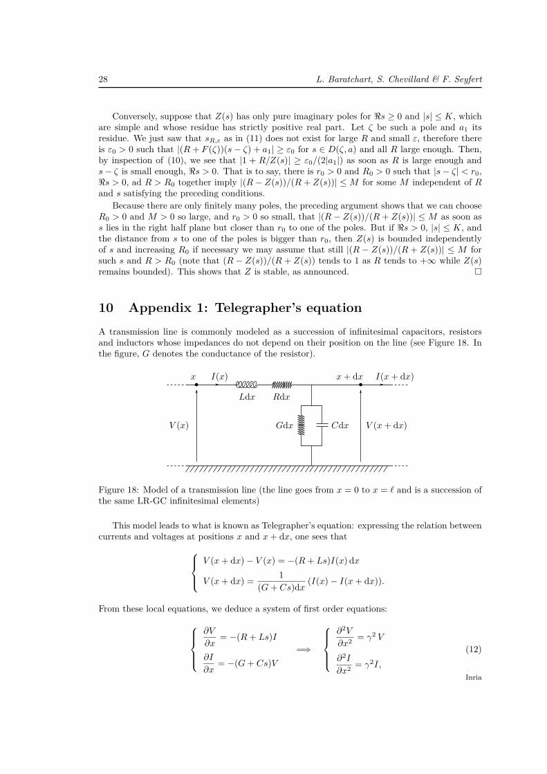
10 Appendix 1: Telegrapher’s equation
A transmission line is commonly modeled as a succession of infinitesimal capacitors, resistorsand inductors whose impedances do not depend on their position on the line (see Figure 18. Inthe figure, G denotes the conductance of the resistor).
Figure 18: Model of a transmission line (the line goes from x = 0 to x = ` and is a succession ofthe same LR-GC infinitesimal elements)
This model leads to what is known as Telegrapher’s equation: expressing the relation betweencurrents and voltages at positions x and x+ dx, one sees that
V (x+ dx)− V (x) = −(R+ Ls)I(x)dx
V (x+ dx) = 1(G+ Cs)dx (I(x)− I(x+ dx)).
From these local equations, we deduce a system of first order equations:∂V
∂x= −(R+ Ls)I
∂I
∂x= −(G+ Cs)V
=⇒
∂2V
∂x2 = γ2 V
∂2I
∂x2 = γ2I,
(12)
Inria
Transfer functions realizable with active electronic components 29
where γ is one of the complex square roots of (R+ Ls)(G+ Cs).We set z0 = (R+ Ls)/γ, so that we can write R+ Ls = γ z0 and G+ Cs = γ
z0.
Since R, G, L and C do not depend on x, Equation (12) leads to the following explicitsolutions: V (x) = A exp(γ x) +B exp(−γ x)
I(x) = D exp(γ x) + E exp(−γ x).(13)
The transmission line has a given length ` and we want to express the relations between I(0),V (0), I(`) and V (`). For this purpose, we simply need to express the constants A, B, D and Ein function of I(0) and V (0).
On the one hand, V (0) = A + B and I(0) = D + E by letting x = 0 in Equation (13). Onthe other hand, differentiating Equation (13) at point x = 0, we get
∂V
∂x(0) = γ (A−B)
∂I
∂x(0) = γ (D − E).
(14)
Now, using Equation (12) at x = 0, we see that ∂V∂x
(0) = −γ z0 I(0) and ∂I
∂x(0) = − γ
z0V (0),
thus B −A = z0 I(0) and E −D = V (0)/z0. This gives us the values of A, B, D and E:
A = 12 (V (0)− z0 I(0))
B = 12 (V (0) + z0 I(0))
D = 12 (I(0)− V (0)/z0)
E = 12 (I(0) + V (0)/z0).
(15)
Finally, putting these constants in Equation (13), at point x = `, and collecting the terms inI(0) and in V (0), we obtain:
V (`) = cosh(γ `)V (0) − z0 sinh(γ `) I(0)
I(`) = − sinh(γ `)z0
V (0) + cosh(γ `) I(0).(16)
The second line of Equation (16) gives us
V (0) = z0 coth(γ `) I(0)− z0
sinh(γ `) I(`),
which we inject in the first line of the system, leading to
V (`) = z0
sinh(γ `) I(0)− z0 coth(γ `) I(`).
Remark that multiplying R, G, L and C by some constant α does not change the value ofz0, but has the effect of multiplying γ by α. Therefore, the relations between the currents andvoltages at the terminals of a line of length ` with characteristics R, G, L and C are the samethat the relations at the terminals of a line of length 1 with characteristics R/`, G/`, L/` and
RR n° 8659
30 L. Baratchart, S. Chevillard & F. Seyfert
C/`. In conclusion, from a theoretical viewpoint, the length of the line can be arbitrary and isnot worth mentioning. We arbitrarily set it to 1 in this report.
Note that, by convention, all currents are oriented so as to enter electronic components. InFigure 2 on page 5, we hence have I1 = I(0), but I2 = −I(`).
Lemma 12. When <(s) ≥ 0, we have <(V1 I1 + V2 I2) ≥ 0.
Proof. We remark that
V1 I1 + V2 I2 = V (0) I(0)− V (`) I(`)
= −∫ `
0
(∂V
∂x(ξ) I(ξ) + V (ξ) ∂I
∂x(ξ))
dξ.
Replacing ∂V/∂x and ∂I/∂x by their values in function of I and V , as given by Equation (12),we obtain
V1 I1 + V2 I2 = −∫ `
0
(−(R+ Ls) |I(ξ)|2 − (G+ Cs) |V (ξ)|2
)dξ.
Finally, we get that
<(V1 I1 + V2 I2) =∫ `
0(R+ L<(s)) |I(ξ)|2 + (G+ C <(s)) |V (ξ)|2 dξ.
The expression under the integral symbol being positive for <(s) ≥ 0, the integral itself is positivewhen <(s) ≥ 0.
11 Appendix 2: Transfer functions and stabilityIn this section, we discuss transfer functions in connection with stability and harmonic response,a thorough account of which seems hard to find in the literature.
On the real line R, we let L1(R), L2(R) and L∞(R) indicate respectively the spaces ofcomplex-valued summable, square summable, and essentially bounded measurable functions withrespective norms
‖f‖L1(R) =∫ +∞
−∞|f(t)| dt, ‖f‖L2(R) =
(∫ +∞
−∞|f(t)|2 dt
)1/2
(17)
and‖f‖L∞(R) = sup
A ≥ 0 : m
(x ∈ R; |f(x)| > A
)> 0, (18)
where m(E) stands for Lebesgue measure of a set E. We put L1loc(R) (resp. L2
loc(R), L∞loc(R))for spaces of functions f such that χEf ∈ L1(R) (resp. L2(R), L∞(R)) whenever E is a boundedmeasurable subset of R, where χE stands for the characteristic function of E (which is 1 on Eand 0 elsewhere). We shall have to deal with corresponding spaces when R gets replaced by theimaginary axis iR, or by the positive semi-axis R+ = [0,∞). We then write L1(iR), L1(R+),and so on.
In order to study even fairly common systems1, one cannot work entirely with functions andit is convenient to use the distributional formalism as follows. Let D(R) be the space of smooth(i.e. C∞) functions with compact support on R; recall that the support of ϕ, abbreviated as
1For instance transmission lines like in the previous Appendix.
Inria
Transfer functions realizable with active electronic components 31
suppϕ, is the closure of those t ∈ R with ϕ(t) 6= 0. A distribution [12, ch. 6] is a form (i.e. acomplex-valued linear map) Φ on D(R) which is continuous in the sense that to each compactK ⊂ R, there is a constant C and an integer n ≥ 0 for which |〈Φ, ϕ〉| ≤ C‖ϕ(k)‖L∞(R) for all0 ≤ k ≤ n, whenever ϕ ∈ D(R) is supported on K; here and below, brackets indicate the actionof distributions and superscript (k) stands for the k-th derivative. Each f ∈ L1
loc(R) identifieswith a distribution upon setting 〈f, ϕ〉 =
∫R fϕ. Distributions can be multiplied by smooth
functions: if ψ ∈ C∞(R), then ψΦ is the distribution given by 〈ψΦ, ϕ〉 = 〈Φ, ψϕ〉. They can bedifferentiated as well, the derivative of Φ being given by 〈Φ(1), ϕ〉 = −〈Φ, ϕ(1)〉. Also, if Φ is adistribution and ψ lies in D(R), the convolution Φ ∗ ψ is the function Φ ∗ ψ(t) = 〈Φ, ψ(t − .) 〉;here, the dot in the argument stands for a dummy variable. The support suppΦ of a distributionΦ is the complement of the largest open set Ω for which 〈Φ, ϕ〉 = 0 whenever suppϕ ⊂ Ω.
Let us think of t ∈ R as being time. A linear dynamical system is a linear map u 7→ y sendingeach u belonging to a certain function space of the variable t (the admissible inputs) to a functiony of t (the output corresponding to u), which is causal (i.e. u(t) = 0 for t ≤ t0 implies the sameis true for y) and time invariant (if y is the output corresponding to some admissible u and ifτ ∈ R, then u(.− τ) is admissible and y(.− τ) is the corresponding output). If inputs from D(R)are admissible and generate continuous outputs, then under mild continuity assumptions2 thereis a distribution Φ supported on R+ allowing us to describe the system through the convolutionequation:
y(t) = (Φ ∗ u)(t), u ∈ D(R). (19)
Moreover inputs from D(R) turn out to generate smooth outputs [12, thm. 6.33]. The distri-bution Φ is called the impulse response of the system as it corresponds formally to the outputgenerated by a Dirac-δ input. What we defined really is a scalar system, that is, one whoseinput and output are real or complex valued. The more general case of vector-valued (finitedimensional) input and output can be represented as a matrix of scalar systems. For mattersunder consideration here, results for vector-valued inputs and outputs are immediately deducedby concatenation from their scalar-valued analogs.
Let now S(R) be the Schwartz space of smooth functions whose derivatives of any orderdecrease faster than every polynomial at infinity. A distribution Ψ is called tempered if itextends to a form on S which is continuous in that there are integers n,m ≥ 0 and a constant Cfor which |〈Ψ, ϕ〉| ≤ C‖(1 + |.|m)ϕ(k)‖L∞(R) for all 0 ≤ k ≤ n, whenever ϕ ∈ S(R). Now, if Φ isa distribution supported on R+ such that the distribution e−A· Φ is tempered for some A ∈ R,then we say that Φ is Laplace transformable (or A-Laplace transformable if some A needs to bespecified) and we can define its Laplace transform L(Φ) as a function of the complex variables = x+ iy defined on the semi-infinite strip x > A by the rule:
L(Φ)(s) = 〈Φ, e−s·〉. (20)
Notation (20) deserves a word of explanation: although Φ cannot be applied, strictly speaking, tothe function on R+ given by t 7→ e−st, <s > A, the latter can be smoothly extended for negativet so as to vanish, say for t ≤ −1. The tempered distribution e−A· Φ may then be applied to eA·times this extension which lies in S(R), and the fact that Φ is supported on R+ entails that theresult is independent of the extension used. This is what is meant by (20). It can be shownthat the latter defines a holomorphic function of s for <s > A [9, thm. 8.3.1]. If Φ happensto be a locally integrable function, say f ∈ L1
loc(R), then it is easy to see that it is A-Laplacetransformable if and only if e−A·f ∈ L1(R) and that (20) reduces to the standard definition of
2If un ⊂ D(R) is supported on a compact set K and u(k)n converges to u(k) uniformly on K for each k ≥ 0
and some u ∈ D(R), the corresponding outputs yn should converge pointwise to the output associated with u.
RR n° 8659
32 L. Baratchart, S. Chevillard & F. Seyfert
Laplace transform:
L(f)(s) =∫ ∞
0e−stf(t) dt. (21)
Note for later use that if Φ is Laplace transformable, then its derivative is again Laplace trans-formable and L(Φ(1))(s) = sL(Φ)(s). This follows easily from the definition.
When Φ is A-Laplace transformable and u ∈ D(R), then y given by (19) is in turn A′-Laplacetransformable for all A′ > A. Indeed, it holds that
e−A′t|y(t)| =
∣∣∣e−A′t〈Φ, u(t− .)〉∣∣∣ = e−(A′−A)t
∣∣∣〈e−A·Φ, e−A(t−.)u(t− .)〉∣∣∣ (22)
≤ e−(A′−A)tC∥∥∥(1 + |.|m)
(e−A·u
)(n)∥∥∥L∞(R)
= C ′e−(A′−A)t, (23)
where we used continuity properties of tempered distributions. Thus, since Laplace transformconverts convolutions into ordinary products much like Fourier transform does [9, eqn. 8.5.8],we get that
L(y)(s) = L(Φ)(s)L(u)(s), <s > A. (24)
Equation (24) is the so-called frequency description of (19), and L(Φ) is called the transferfunction of the system. Note that the restriction of L(y) to the vertical line <s = x > A isthe Fourier transform of e−x·y ∈ L1(R), hence L(y) cannot vanish identically unless y does [11,thm. 9.11]. Consequently, by (24), a system is uniquely defined by its transfer-function when itexists.
Although (19) is initially valid for u ∈ D(R) only, the class of admissible inputs is muchbigger in cases of interest and (24) will usually extend to more general functions. For instanceif continuous inputs with compact support are admissible and generate continuous outputs, andif moreover bounded pointwise convergence of inputs entails pointwise convergence of outputs,then by the Riesz representation theorem [11, thm. 6.19] the impulse response Φ is locally afinite measure, say ν, and (19) becomes
y(t) =∫
[0,t]u(t− τ) dν(τ) (25)
(compare [1, Ch. 1]). Letting |ν| be the total variation of ν, which is a (not necessarily finite)positive measure on R+ [11, ch. 6, sec.1], we find that Φ is A-Laplace transformable if and onlyif t 7→ e−At is summable against |ν|. In this case (24) will hold in some strip <s > A′ as soonas u ∈ L1
loc(R) is of exponential type, meaning there is B ∈ R such that e−B·u ∈ L∞(R). Thislevel of generality is about right for most applications to circuit theory, for solutions to lineardifferential equations with constant coefficients initially at rest can be expressed via convolutionagainst exponential kernels while delays introduced by transmission lines introduce Dirac deltameasures in the impulse response [2, 3].
It has become customary to denote signals (i.e. functions of t) by lower case letters andtheir Laplace transforms with corresponding upper case letters. Real-valued signals t 7→ u(t)correspond under Laplace transform to conjugate-symmetric functions: U(s) = U(s). System(19) maps real signals to real signals if and only if Φ is real-valued on real functions, whichresults in the transfer function being conjugate symmetric. System theory is mostly concernedwith real-valued signals although such a restriction is rather immaterial as far as theory goes.
What precedes is enough to bring formal meaning to most computations, as long as pointwiseevaluation in (24) is restricted to some strip where every Laplace transform involved does exist.However, when dealing with issues of passivity and stability, square summable inputs and outputs
Inria
Transfer functions realizable with active electronic components 33
are of special significance (these are the signals of finite energy) and a more refined interpretationof (24), valid on the imaginary axis, becomes necessary.
Clearly if f ∈ L2(R+), then it is A-Laplace transformable for each A > 0 because f(t)e−at issummable by the Schwarz inequality. Its Laplace transform F is thus defined and holomorphicfor <s > 0 and, as can be surmised from (21) and rigorously proved [7, ch. 8], the limitF (iy) = limx→0 F (x+ iy) exists for almost every y ∈ R and coincides with the Fourier transformf(y) defined for almost every y ∈ R by the formula
f(y) = limB→+∞
∫ B
0e−iytf(t) dt. (26)
The limit in (26) holds in the L2-sense by Plancherel’s theorem [11, thm. 9.13]. The fact thatit also holds pointwise almost everywhere is a deep result after the work of Carleson [6, thm.11.1.1]. Furthermore, putting Fx(y) = F (x + iy), we have that limx→0 ‖Fx − f‖L2(R) = 0 andalso that
supx>0
∫ +∞
−∞|F (x+ iy)|2 dy <∞. (27)
In fact the supremum in (27) is ‖f‖2L2(R), which is in turn equal to 2π‖f‖2
L2(R+) by the essentiallyisometric character of the Fourier transform. It is a theorem of Paley and Wiener that the spaceof all functions F holomorphic in the right half-plane and satisfying (27) coincides with the setof Laplace transforms of functions f ∈ L2(R+). When normed with the square root of the lefthand side of (27), the latter becomes a Hilbert space known as the Hardy space of exponent 2of the right half plane [7, Ch. 8]3, hereafter denoted by by H2. The norm of a Hardy functionF ∈ H2, indicated with ‖F‖2, is thus
√2π times the energy of the signal of which it is the
Laplace transform. Conjugate symmetric H2-functions. form a real Hilbert subspace of H2.We need also introduce the Hardy space H∞ of bounded analytic functions in <s > 0
endowed with the sup norm. As is the case for H2 functions, the limit F (iy) = limx→0 F (x+ iy)exists for almost every y ∈ R when F ∈ H∞ [7, ch. 8]. Moreover, this limit function lies inL∞(iR), and it holds that
‖F‖L∞(iR) = sup<s>0
|F (s)|. (28)
The quantity in (28) is the H∞-norm of F that we abbreviate as ‖F‖∞.Consider now a linear dynamical system mapping L2(R+) into itself, that is, the system maps
inputs of finite energy to outputs of finite energy Such a system we call stable. It is remarkablethat it is automatically continuous as a map, that is, there is a constant C ≥ 0 such that‖y‖L2(R+) ≤ C‖u‖L2(R+) [10, thm. 4.1.1]. Taking Laplace transforms, we find that the systeminduces a continuous linear map from H2 into itself that commutes with multiplication by e−sτfor all τ ∈ R+. As it turns out [10, Cor. 3.2.4], such a linear map is just multiplication by someH ∈ H∞, and its norm is ‖H‖∞. Next, pick a < 0 and consider the function G(s) = H(s)/(s−a).Because H ∈ H∞, it is easy to check that G ∈ H2 hence by the Paley Wiener theorem there isg ∈ L2(R+) such that G = L(g). If we regard g as a distribution, we find that H = L(g(1)− ag).Thus, since a system is uniquely defined by its transfer function, we conclude that our initialsystem has Laplace transformable impulse response g(1)−ag and transfer function H. To recap,a system is stable if and only if it has a transfer function lying in H∞, and the maximum gainis the H∞-norm of the transfer function. We also gather from what precedes that the impulseresponse is of the form g(1) − ag with g ∈ L2(R+), a < 0, and that every function in H∞ arises
3More generally, one defines the Hardy space Hp, 1 ≤ p <∞, to consist of holomorphic functions in the righthalf plane such that supx>0 ‖F (x+ .)‖Lp(iR) <∞., see [7, ch.8]
RR n° 8659
34 L. Baratchart, S. Chevillard & F. Seyfert
as the transfer function of a stable system. However, not every g ∈ L2(R+) gives rise to theimpulse response of a stable system via Φ = g(1)−ag for some a < 0. In fact, no non-tautologicalcharacterization is known of those Laplace transformable distributions whose Laplace transformbelongs to H∞, compare [9, thm. 8.7.1].
A stable system can be fed with an input u ∈ L∞loc(R+) (extended by 0 for negative t) because,by causality, the output at time t ≤ t0 is the same as if we used the input χ[0,t0]u which lies inL2(R+). In order to gain physical understanding of the transfer function, it is worth estimatingthe asymptotic behavior, as t → +∞, of the output generated by the input u(t) = χR+(t)eiωtfor fixed ω ∈ R. Dwelling on what precedes, let the system have transfer function H ∈ H∞and impulse response Φ = g(1) − ag with g ∈ L2(R), a < 0. Due to the distributional natureof the derivative g(1) appearing in Φ, we cannot bluntly plug in (19) the input u which is non-smooth at zero and has infinite support. To circumvent this, let ϕ ∈ D(R) be non-negative,supported on [−1, 1], even, and such that
∫ϕ(t) dt = 1. For ε ∈ (0, 1], set ϕε(t) = ϕ(t/ε)/ε and
φε(t) =∫ t−1 ϕε(τ) dτ . Pick T > 2, define φε,T (t) = φε(t)φε(T − t), and put uε,T (t) = φε,T (t)eiωt.
By construction uε,T ∈ D(R), hence using (19) we obtain the corresponding output yε,T by theformula:
yε,T (t) = eiωt∫Rg(τ)
(φ
(1)ε,T (t− τ) + (iω − a)φε,T (t− τ)
)e−iωτ dτ (29)
= eiωt((ge−iω· ∗ ϕε
)(t)−
(ge−iω· ∗ ϕε(T − .)
)(t) + (iω − a)
(ge−iω· ∗ φε,T
)(t)).
When ε tends to 0, then uε,T converges in L2(R) to uT = χ[0,T ]eiω· so that yε,T must converge to
the corresponding output yT , as the system is stable. Now, since ge−iω· ∈ L2(R) (when extendedby zero for negative arguments), it is standard that ge−iω·∗ϕε → ge−iω· in L2(R) [13, thm. 1.6.1]and by the same token we get that ge−iω· ∗ ϕε(. − T ) → g(. − T )e−iω (.−T ). Moreover, becauseφε,T converges to χ[0,T ] in L1(R), it follows from Minkowski’s inequality for integrals [11, ch. 7,ex. 4] that ge−iω· ∗ φε,T → ge−iω· ∗ χ[0,T ] in L2(R). Altogether, we find that
yT (t) = g(t)− g(t− T )eiωT + eiωt(iω − a)∫ t
max(0,t−T )g(τ)e−iωτ dτ.
Next, let y be the output associated with u(t) = χR+(t)eiωt. By causality it must coincide withyT on [0, T ], therefore using that g is supported on R+ we obtain:
y(t) = g(t) + eiωt(iω − a)∫ t
0g(τ)e−iωτ dτ. (30)
If we let now t → +∞ and take into account that (26) converges pointwise almost everywherewhile using the relation (iω − a)L(g)(iω) = H(iω), we find that for almost every ω
y(t) = g(t) +H(iω)eiωt + o(1), t→ +∞. (31)
which is the formula we are aiming for. It says that, for almost every ω, the output y(t)asymptotically winds at constant angular speed ω on the boundary of a tubular neighborhoodof t 7→ g(t) having radius |H(iω)|. In general, the behavior at exceptional frequencies for which(31) does not hold can be quite chaotic. Note that g depends on a but not on ω, hence (31)shows that the limiting behavior of g(t) for large t depends only on the system. Whereas g needs
Inria
Transfer functions realizable with active electronic components 35
not tend to 0 at infinity4 it is nevertheless small “most of the time” since obviously
m(t : t ≥ t0, |g(t)| > α
)≤‖g‖2
L2([t0,+∞))
α2
which goes to 0 as t0 → +∞. Thus, asymptotically in time, the output resulting from a periodicinput with pulsation ω is “most of the time and for almost every ω” close to a signal havingsame period, gain |H(iω)|, and phase shift argH(iω). When g tends to zero at infinity, theresult is neater as the words “most of the time” can be omitted from the previous sentence. Thisoccurs for instance if Φ ∈ L1(R+), as follows easily by dominated convergence from the formulag = Φ ∗ (χR+(.)ea·); in this case (31) holds in fact for every ω.
Difficulties connected with the asymptotic behavior of g disappear if instead of χR+(t)eiωtwe use an input achieving a smooth transition between the zero function and t 7→ eiωt, likeu(t) = φ1(t)eiωt where φ1(t) =
∫ t0 ϕ(τ)dτ was defined earlier. Then, taking into account that
suppϕ ⊂ [−1, 1], a computation similar to (29) with Φε,T (t) replaced by φ(t)φε(T − t) leads to
y(t) = (g ∗ ϕ)(t) + +eiωt(iω − a)(∫ t−1
0g(τ)e−iωτ dτ +
∫ t+1
t−1g(τ)e−iωτϕ(t− τ) dτ
)(32)
instead of (30). Because g ∈ L2(R+), both (g ∗ ϕ)(t) and the last integral in (32) tend to zeroas t→ +∞ by the Schwarz inequality, so the term g(t) is no longer present in (31). It is worthobserving that a similar conclusion is reached when Φ ∈ L2(R+), a condition that does notsubsume stability but allows for some unstable systems.
This interpretation of the transfer function as an asymptotic multiplier frequency-wise inresponse to harmonic inputs is of great importance in design.
References[1] Laurent Baratchart. Sur l’approximation rationnelle L2 pour les systèmes dynamiques
linéaires. thèse de doctorat ès sciences, Université de Nice, Septembre 1987.
[2] Belevitch. Classical network theory. series in information systems. Holden Days, 1968.
[3] Herbert Carlin and Pier Paolo Civalleri. Wideband circuit design. Electronic engineeringsystems series. CRC Press, 1998.
[4] H.J. Carlin and D.C. Youla. Network synthesis with negative resistors. Proceedings of theIRE, 49(5):907–920, 1961.
[5] Pierre Faure, Michel Clerget, and cois Germain, Fran˙Opérateurs rationnels positifs. Méth-odes Mathématiques de l’Informatique. Dunod, 1979.
[6] Loukas Grafakos. Modern Fourier analysis. Number 250 in Grad. Texts in Maths. Springer,2009.
[7] Kenneth Hoffman. Banach spaces of analytic functions. series in modern analysis. Prentice-Hall, 1962.
4If we let Φ =∑
k∈N χR+ (. − tk)eαk(.−tk) with αk = b + iβk where b < 0 and βk ∈ R, then H(s) =∑ke−tks/(s − αk) will lie in H∞ if |βk| tends to infinity sufficiently fast but g = Φ ∗ (χR+ (.)ea·) does tend to
zero at infinity. A real-valued example is obtained upon taking the αk in conjugate pairs.
RR n° 8659

36 L. Baratchart, S. Chevillard & F. Seyfert
[8] K. Kurokawa. Power waves and the scattering matrix. Microwave Theory and Techniques,IEEE Transactions on, 13(2):194–202, Mar 1965.
[9] O. P. Misra and J.L. Lavoine. Transform analysis of generalized functions, volume 119 ofMathematics Studies. North-Holland, 1986.
[10] Jonathan Partington. Linear operators and linear systems. Number 60 in Student texts.London Math. Soc., 2004.
[11] Walter Rudin. Real and complex analysis. Mc Graw-Hill, 1982.
[12] Walter Rudin. Functional Analysis. International Series in Pure and Applied Mathematics.Mc Graw-Hill, 2 edition, 1991.
[13] P. Ziemer, William. Weakly Differentiable Functions. Number 120 in Grad. Texts in Maths.Springer, 1989.
Inria


RESEARCH CENTRESOPHIA ANTIPOLIS – MÉDITERRANÉE
2004 route des Lucioles - BP 9306902 Sophia Antipolis Cedex
PublisherInriaDomaine de Voluceau - RocquencourtBP 105 - 78153 Le Chesnay Cedexinria.fr
ISSN 0249-6399