Embed Size (px)
Citation preview
J. Electrochem. Sci. Technol., 2018, 9(4), 308-319
− 308 −
One Step Electrodeposition of Copper Zinc Tin Sulfide Using
Sodium Thiocyanate as Complexing Agent
Rabiya Sani, R. Manivannan, and S. Noyel Victoria*
Department of Chemical Engineering, National Institute of Technology Raipur, Chhattisgarh 492010, India
ABSTRACT
Single step electrodeposition of Cu2ZnSnS4 (CZTS) for solar cell applications was studied using an aqueous thiocyanate
based electrolyte. The sodium thiocyanate complexing agent was found to decrease the difference in the deposition poten-
tial of the elements. X-ray diffraction analysis of the samples indicates the formation of kesterite phase CZTS. UV-vis stud-
ies reveal the band gap of the deposits to be in the range of 1.2 - 1.5 eV. The thickness of the deposit was found to decrease
with increase in pH of the electrolyte. Nearly stoichiometric composition was obtained for CZTS films coated at pH 2 and
2.5. I-V characterization of the film with indium tin oxide (ITO) substrate in the presence and the absence of light source
indicate that the resistance decrease significantly in the presence of light indicating suitability of the deposits for solar cell
applications. Results of electrochemical impedance spectroscopic studies reveal that the cathodic process for sulfur reduc-
tion is the slowest among all the elements.
Keywords : CZTS, Electrodeposition, Solar cells, Sodium thiocyanate
Received : 9 May 2018, Accepted : 2 August 2018
1. Introduction
With tremendous growth in the world’s population,the energy demand also increases proportionately [1].The energy demand in 2025 is expected to be twicethat of today’s energy demand, which is approxi-mately 15 TW [1]. Though majority of this demand isfulfilled by the fossil fuels, they are not promisingenergy sources forever and they also pose pollutionproblems [2]. The reliable alternative to fulfill thisenergy requirement is solar energy [2]. Majority ofthe solar cells used today are single crystal silicon orpolycrystalline silicon type which are indirect band-gap materials [3]. Apart from being expensive, sili-con suffers from the disadvantage of having lowabsorption coefficient. This requires a very thickabsorber layer for silicon based solar cells for effec-tive absorption [3]. To overcome these constraints,the focus has turned towards thin film solar technolo-
gies using direct bandgap materials as absorber mate-rials [4]. Commonly used absorber materials for thinfilm photovoltaic technologies are copper indiumgallium diselenide (CIGS), copper indium diselenide(CIS) and cadmium telluride (CdTe) [5]. With limitedavailability of indium (In) and selenium (Se) alongwith toxicity issues arising out from the cadmiumusage, the search for suitable absorber material forthin film technology is still going on [5]. Studies insearch of an inexpensive and environmental friendlyabsorber material with direct band gap have identi-fied Cu2ZnSnS4 (CZTS) as the promising candidatewhich is a quaternary semiconductor with highabsorption coefficient of 104 cm-1 [6]. The highestreported photoconversion efficiency for CZTS basedsolar cells is 12.6% according to the studies in 2014[6]. Like other photovoltaic materials, CZTS thinfilms can also be prepared by various physical andchemical routes [1]. High energy techniques such asatom beam sputtering, radio frequency (RF) magne-tron sputtering, thermal evaporation, pulsed laserdeposition, spray pyrolysis have been employed to
*E-mail address: [email protected]
DOI: https://doi.org/10.5229/JECST.2018.9.4.308
Research Article
Journal of Electrochemical Science and Technology
Rabiya Sani et al. / J. Electrochem. Sci. Technol., 2018, 9(4), 308-319 309
form CZTS thin films [1]. On the other hand, lowenergy techniques such as sol-gel spin coating, chem-ical spray pyrolysis, successive ionic layer adsorptionand reaction, chemical bath deposition, electrochemi-cal deposition have also been employed to formCZTS thin films [7]. Among these low energy routes,electrochemical deposition of CZTS is the mostpromising technology [3]. The first study on electro-chemical deposition of CZTS reported multistepelectrochemical deposition of CZT followed by sul-furization during annealing [8]. Electroplating wasalso studied to deposit CZT followed by high tem-perature annealing in sulfur environment [9]. Multi-step electrodeposition with high temperatureannealing with different electrolytes has been stud-ied extensively [9-12]. In a study on multistep elec-trodeposition of CZTS, a cyanide-free electrolyticbath consisting of the Cu, Sn and Zn precursors wasused as electrolyte for Cu, Zn and Sn co-electrodepo-sition on Mo coated glass slides. After coating of Cu,Zn and Sn on the Mo substrate, sulfur was added tothe deposits by sulfurization in Ar/H2S environmentwith 5 vol% H2S. The CZTS film thus formed wasused to fabricate the solar cell which showed an effi-ciency of 3.4% [9]. In another study, multistep under-potential electrodeposition called as electrochemicalatomic layer epitaxy (ECALE) was used to depositCZTS [11]. Co-electrodeposition where two or moremetals are deposited in a single step is preferred tomultistep electrodeposition processes. Co-electrode-position processes generally involve selection of pre-cursors which are very close to each other inelectromotive force (e.m.f) series or use of complex-ing agent which reduces the differences in the deposi-tion potential [13]. Co-electrodeposition of Cu, Znand Sn followed by sulfurization during annealinghas also been reported [14,15]. One critical issue withsulfur incorporation during annealing is the volumet-ric expansion of the CZTS layer which has negativeimpact on the performance [16-18]. To overcome thisissue, single step electrodeposition incorporating sul-fur during electrodeposition has been proposed[16,17,19]. The major concern with single step elec-trodeposition of CZTS is the widely spaced reductionpotentials of Cu, Zn, Sn and S [20]. The standardreduction potential of Cu, Zn and Sn in uncomplexedstate are +0.34 V, -0.76 V and -0.14 V respectively[8,21]. With significant difference in the standardreduction potentials of Cu, Zn and Sn, the role of
complexing agents in shifting the reduction potentialsto achieve CZTS deposits of desired stoichiometry ina single step is inevitable [21]. In many co-electrode-position processes involving multiple elements, com-plexing agents are useful to bring the reductionpotentials of the elements closer as already men-tioned [20,22]. Trisodium citrate, tartaric acid andsorbitol have been found to be suitable complexingagents for single step electrodeposition of CZTS onmetal and on transparent conducting oxide substrates[15-17,24,25]. In a study on single step electrodepo-sition of CZTS on ITO coated substrate, tri-sodiumcitrate and tartaric acid were used as the complexingagents. The deposition potential used for cathodicelectrodeposition process was -1.05 V vs. SCE. Thedeposits were then annealed in Ar environment at550oC for 1 h. The CZTS deposits were found tohave desired stoichiometry of 2:1:1:4 for Cu:Zn:Sn:S[17]. Sodium thiocyanate is one of the most com-monly used complexing agents in many commercialelectroplating formulations. Use of sodium thiocya-nate for CGS electrodeposition has been reported[21]. Recently, our group reported the use of sodiumthiocyanate as the complexing agent for single stepelectrodeposition of CZTS with an electrolyte con-sisting of 20 mM Cu, Zn, Sn and S and 2.5 M sodiumthiocyanate [22]. The study showed that the qualityof the deposits was influenced significantly by the pHof the electrolyte. However, detailed investigation ofthe behavior of individual precursor in the systemand characterization of the obtained deposits werenot made.
This work discusses in detail single step electro-chemical deposition of CZTS on transparent indiumtin oxide (ITO) substrate using sodium thiocyanate asthe complexing agent. The work also discusses theeffect of pH of the electrolyte used for the depositionon the stoichiometry of the CZTS deposits formed.The deposits formed were characterized using X-raydiffraction (XRD) for crystalline nature, UV-visspectroscopy (UV-vis) for optical properties, scan-ning electron microscopy (SEM) and transmissionelectron microscopy (TEM) for morphology, field -emission gun scanning electron microscopy (FEG-SEM) for thickness of the deposit, energy dispersiveX-ray diffraction (EDX) for elemental composition.The resistance of the deposits was studied by IV-characterization technique. The behavior of the indi-vidual species in the system was investigated using
310 Rabiya Sani et al. / J. Electrochem. Sci. Technol., 2018, 9(4), 308-319
electrochemical impedance spectroscopy (EIS) stud-ies.
2. Material and Methods
2.1 Material
Indium tin oxide (ITO) coated glass slide fromSigma-Aldrich was used as the substrate. The elec-trochemical deposition of CZTS was performedunder potentiostatic mode. Analytical grades of cop-per sulfate pentahydrate (CuSO4.5H2O), zinc sulfateheptahydrate (ZnSO4.7H2O), tin chloride (SnCl2) andsodium thiosulfate (Na2S2O3) were used as Cu, Zn,Sn and S precursors respectively. Sodium thiocyanatewas used as the complexing agent. Deionized waterbubbled with nitrogen was used to prepare the elec-trolyte. The electrolytic bath used for the electrode-position contained 20 mM of Cu, Sn, and S precursoreach and 50 mM of Zn precursor. The concentrationof sodium thiocyanate was maintained at 2 M. ThepH of the electrolyte was adjusted using either KOHor HNO3 solution.
2.2 Experimental
The electrochemical deposition studies were car-ried out in an electrochemical workstation (CHI660E, CH instruments, USA). A three electrode cellconfiguration was used for the deposition experi-ments. Working electrode was formed from ITOglass slide of 10 mm × 10 mm × 1.1 mm dimension,Ag/AgCl was used as the reference electrode whileplatinum wire was used as the counter electrode. Thesuitable deposition potential for the potentiostaticdeposition runs was found out from cyclic voltamme-try (CV) runs of the electrolyte containing all the pre-cursors wi th the complexing agent . Cycl icvoltammetry was also performed for the electrolytescontaining single precursor without and with thecomplexing agent. The CV runs were performed witha scan rate of 0.05 Vs-1. The deposition was doneunder potentiostatic mode for 20 min. The deposits,thus obtained, were washed with deionized water anddried with nitrogen. The deposits were also annealedat 600oC in inert environment. The electrochemicalimpedance spectroscopy was conducted for the indi-vidual precursors with 2 M complexing agent at pH2.5. The deposition potential corresponding to pH 2.5was used to perform the EIS runs. The EIS runs wereconducted for a frequency range from 105 Hz to 1 Hz
with potential amplitude of 10 mV rms was used. Theresults of the EIS runs were analyzed using Zsimp-win software. The morphology of the deposits andthe elemental composition were done using SEM(Zeiss Evo-Model EVO 18) and EDX (INCA 250EDS with X-MAX 20mm Detector) respectively.FEG-SEM (JEOL, JSM-7600F) was used for analyz-ing the thickness of the CZTS deposition. TEM(Philips, CM 200) was used for the morphology anal-ysis. The UV-visible spectroscopy was performed bydispersing the CZTS particles from the non-annealeddeposits in deionized water. The optical properties ofthe deposits were characterized using the absorptionspectra of the samples generated in UV-vis spectro-photometer (Shimadzu, UV-1800). Crystalline natureof the deposits was studied using X-ray diffractionunit (PANalytical 3 kW X’pert). I-V characterizationstudies were done using electrochemical workstation(CHI 660E, CH instruments, USA).
3. Results and Discussion
3.1 Cyclic voltammetry
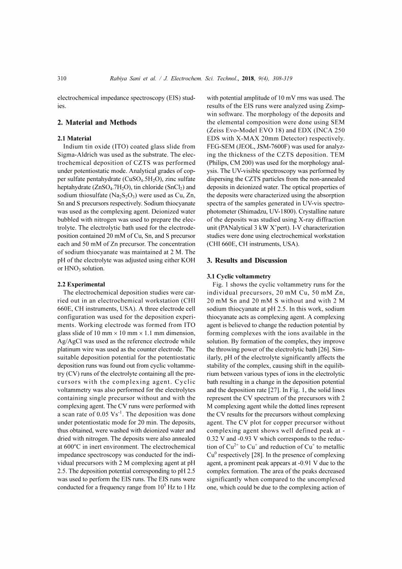
Fig. 1 shows the cyclic voltammetry runs for theindividual precursors, 20 mM Cu, 50 mM Zn,20 mM Sn and 20 mM S without and with 2 Msodium thiocyanate at pH 2.5. In this work, sodiumthiocyanate acts as complexing agent. A complexingagent is believed to change the reduction potential byforming complexes with the ions available in thesolution. By formation of the complex, they improvethe throwing power of the electrolytic bath [26]. Sim-ilarly, pH of the electrolyte significantly affects thestability of the complex, causing shift in the equilib-rium between various types of ions in the electrolyticbath resulting in a change in the deposition potentialand the deposition rate [27]. In Fig. 1, the solid linesrepresent the CV spectrum of the precursors with 2M complexing agent while the dotted lines representthe CV results for the precursors without complexingagent. The CV plot for copper precursor withoutcomplexing agent shows well defined peak at -0.32 V and -0.93 V which corresponds to the reduc-tion of Cu2+ to Cu+ and reduction of Cu+ to metallicCu0 respectively [28]. In the presence of complexingagent, a prominent peak appears at -0.91 V due to thecomplex formation. The area of the peaks decreasedsignificantly when compared to the uncomplexedone, which could be due to the complexing action of
Rabiya Sani et al. / J. Electrochem. Sci. Technol., 2018, 9(4), 308-319 311
thiocyanate ions. A shift in the cathodic peak poten-tial combined with decrease in the peak current den-sity with the addition of complexing agent is reportedto be an indication of better complexing action [29].Similarly, oxidation process is enhanced which isseen by a well defined peak in the anodic sweepwhich is not present in the uncomplexed copper sys-tem. This clearly indicated that the SCN- has bettercomplexing ability with copper precursor [29,30].The cyclic voltammogram for uncomplexed Zn inFig. 1 shows a cathodic peak at -1.2 V correspondingto the reduction of Zn2+ whereas with the addition ofcomplexing agent two cathodic peaks appear, one at -1.1 V which has a peak area lower than the uncom-plexed system and a major peak at -1.3 V indicatingthe presence of more than one form of Zn2+ complexin the electrolyte [31,32]. From Fig. 1, it is seen thatthe addition of complexing agent causes negativeshift of the reduction potential by 205 mV in the caseof Sn precursor. The cathodic peak potential corre-sponding to Sn2+ is -0.8 V without complexing agentwhich decreases to -1.005 V with complexing agent.The current density also showed a significantdecrease with complexing agent corresponding tobetter complexing action.
The cyclic voltammograms for sodium thiosul-phate without complexing agent shown in Fig. 1
presents two cathodic peaks, a smaller peak at -0.95V which correspond to partial decomposition ofS2O3
2- to S and SO32- through electrochemical reac-
tion given in equation 1 in the acidic medium and amore negative well defined peak at -1.27 V whichcould be attributed to the equations 2 and 3 [33].
(1)
(2)
(3)
With the addition of thiocyanate, though any com-plex formation is not anticipated, the peak presents apositive shift and occurs at -1.13V thus decreasingthe reduction potential. Such a positive shift in thereduction potential has been observed in the case ofcyano compounds on protonation [34]. Based on theobservations, addition of thiocyanate thus helps indecreasing the deposition potential window betweenCu, Zn, Sn and S and helps in co-deposition. Theaddition of complexing agents was found to causeshift in reduction potentials due to complex forma-tion with one or many of the ions available in the sys-tem [21-24] . The present observat ion wi ththiocyanate can also be credited to the varying degree
2S2O3
2 –6H
+4e
–+ + SO
3
2 –3S 3H
2O+ +→
SO3
2–6H
+4e
–+ + S 3H
2O+→
S 2e–
+ S2–
→
Fig. 1. Cyclic voltammograms for the individual precursors with and without 2M sodium thiocyanate at pH 2.5.
312 Rabiya Sani et al. / J. Electrochem. Sci. Technol., 2018, 9(4), 308-319
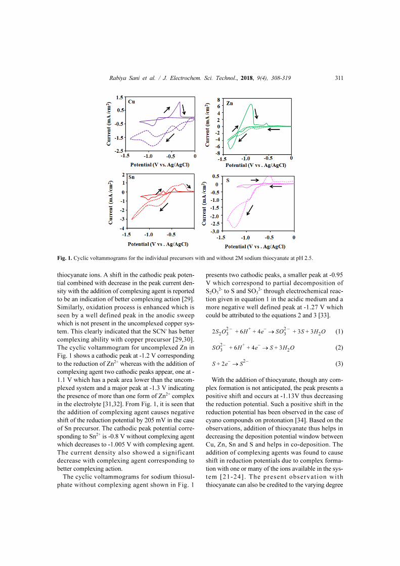
of complexing action of the same with Cu, Zn and Snions available in the electrolyte. Fig. 2 shows the CVpatterns for the electrolyte which consists of all thefour precursors with sodium thiocyanate at pH 1.8, 2,2.5 and 2.8. The cathodic peak potential for the elec-trolytes are -1.139 V for pH 1.8, -1.126 V for pH 2,-0.945 V for pH 2.5 and -0.92 V for pH 2.8. Thecathodic peak current value is the highest for theelectrolytic bath at pH 1.8 which could be due to theincreased concentration of H+ ions and decreased dif-fusion resistance enabling higher deposition rate [35].Change in the reduction potential value with changein pH could be attributed to the involvement of pro-ton during electron transfer reaction [36].
3.2 X-ray diffraction
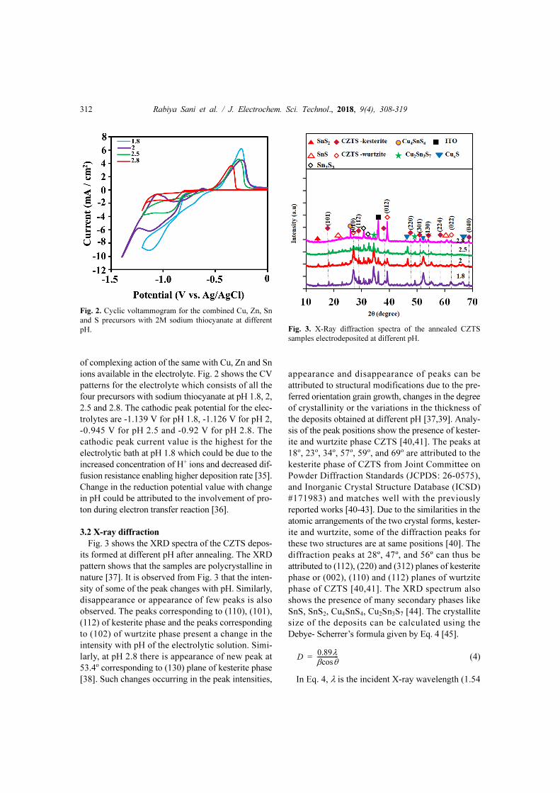
Fig. 3 shows the XRD spectra of the CZTS depos-its formed at different pH after annealing. The XRDpattern shows that the samples are polycrystalline innature [37]. It is observed from Fig. 3 that the inten-sity of some of the peak changes with pH. Similarly,disappearance or appearance of few peaks is alsoobserved. The peaks corresponding to (110), (101),(112) of kesterite phase and the peaks correspondingto (102) of wurtzite phase present a change in theintensity with pH of the electrolytic solution. Simi-larly, at pH 2.8 there is appearance of new peak at53.4o corresponding to (130) plane of kesterite phase[38]. Such changes occurring in the peak intensities,
appearance and disappearance of peaks can beattributed to structural modifications due to the pre-ferred orientation grain growth, changes in the degreeof crystallinity or the variations in the thickness ofthe deposits obtained at different pH [37,39]. Analy-sis of the peak positions show the presence of kester-ite and wurtzite phase CZTS [40,41]. The peaks at18o, 23o, 34o, 57o, 59o, and 69o are attributed to thekesterite phase of CZTS from Joint Committee onPowder Diffraction Standards (JCPDS: 26-0575),and Inorganic Crystal Structure Database (ICSD)#171983) and matches well with the previouslyreported works [40-43]. Due to the similarities in theatomic arrangements of the two crystal forms, kester-ite and wurtzite, some of the diffraction peaks forthese two structures are at same positions [40]. Thediffraction peaks at 28º, 47º, and 56º can thus beattributed to (112), (220) and (312) planes of kesteritephase or (002), (110) and (112) planes of wurtzitephase of CZTS [40,41]. The XRD spectrum alsoshows the presence of many secondary phases likeSnS, SnS2, Cu4SnS4, Cu2Sn3S7 [44]. The crystallitesize of the deposits can be calculated using theDebye- Scherrer’s formula given by Eq. 4 [45].
(4)
In Eq. 4, λ is the incident X-ray wavelength (1.54
D0.89λ
βcosθ---------------=
Fig. 2. Cyclic voltammogram for the combined Cu, Zn, Sn
and S precursors with 2M sodium thiocyanate at different
pH. Fig. 3. X-Ray diffraction spectra of the annealed CZTS
samples electrodeposited at different pH.
Rabiya Sani et al. / J. Electrochem. Sci. Technol., 2018, 9(4), 308-319 313
Å), β is the broadening of diffraction line, full widthat half maximum (FWHM) in radians, θ is the dif-fraction angle of the prominent peak [18,45,46]. Theaverage crystallite size of the deposits considering allthe peaks corresponding to the different crystallitephases for the samples deposited at pH 1.8, 2, 2.5 and2.8 were found to be 30 nm, 23 nm, 28 nm and 30 nmrespectively. The crystallite size presents a mono-tonic trend. Such behavior where a particular param-eter cannot be accounted for the variation incrystallite size has been reported already [47]. In astudy by Aslan et al. the crystallite size of the CZTSpresents continuously increasing trend, however thethickness of the deposits did not present a regularincreasing or decreasing trend. The sulfur content ofthe deposits however, were found to increase withpH. Thus, the crystallite size of the CZTS depositswas found to be influenced by the sulfur content andthe thickness of the deposits [47]. A similar behaviorhas been observed for the crystallite size in the pres-ent study which could be attributed to the thicknessand the sulfur content, a part of which may evaporateduring annealing affecting the morphology of thedeposits.
3.3 UV vis spectroscopy
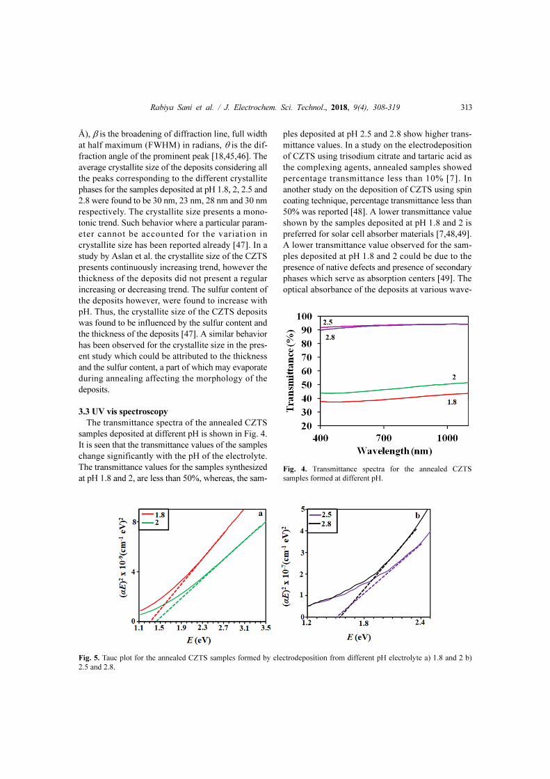
The transmittance spectra of the annealed CZTSsamples deposited at different pH is shown in Fig. 4.It is seen that the transmittance values of the sampleschange significantly with the pH of the electrolyte.The transmittance values for the samples synthesizedat pH 1.8 and 2, are less than 50%, whereas, the sam-
ples deposited at pH 2.5 and 2.8 show higher trans-mittance values. In a study on the electrodepositionof CZTS using trisodium citrate and tartaric acid asthe complexing agents, annealed samples showedpercentage transmittance less than 10% [7]. Inanother study on the deposition of CZTS using spincoating technique, percentage transmittance less than50% was reported [48]. A lower transmittance valueshown by the samples deposited at pH 1.8 and 2 ispreferred for solar cell absorber materials [7,48,49].A lower transmittance value observed for the sam-ples deposited at pH 1.8 and 2 could be due to thepresence of native defects and presence of secondaryphases which serve as absorption centers [49]. Theoptical absorbance of the deposits at various wave-
Fig. 4. Transmittance spectra for the annealed CZTS
samples formed at different pH.
Fig. 5. Tauc plot for the annealed CZTS samples formed by electrodeposition from different pH electrolyte a) 1.8 and 2 b)
2.5 and 2.8.
314 Rabiya Sani et al. / J. Electrochem. Sci. Technol., 2018, 9(4), 308-319
lengths was analyzed and the data were used to gen-erate the absorption coefficient values, which wereused to plot the Tauc plot shown by the Tauc relation(Eq. 5) [50].
(5)
In equation 5, α is the absorption coefficient, A is aconstant, hν is the photon energy (E) and Eg is the band-gap energy. The superscript N in equation 5, is a con-stant which takes the values 1/2, 3/2 and 3 for directallowed, indirect forbidden and indirect allowed materi-als respectively [16,17,24]. Figs. 5 (a-b) shows the cor-responding Tauc plots for the CZTS deposits formed atdifferent pH in visible spectrum. It is clearly seen thatthe bandgap value changes with the pH. The band gapvalue for the samples are 1.22 eV, 1.2 eV, 1.5 eV and1.4 eV for pH 1.8, 2, 2.5 and 2.8 respectively whichmatches well with the reported literature [16,17]. In asimilar study on investigation of the effect of pH on thequality of the CZTS deposits, changes in the band gapvalue with change in pH was attributed to the presenceof secondary phases [51]. It is clearly seen from theXRD analysis that the secondary phases present in thedeposited film differ with the pH. The band gap of oneof the secondary phases Cu2SnS3 is 1.15 eV [51].
3.4 Scanning electron microscopy
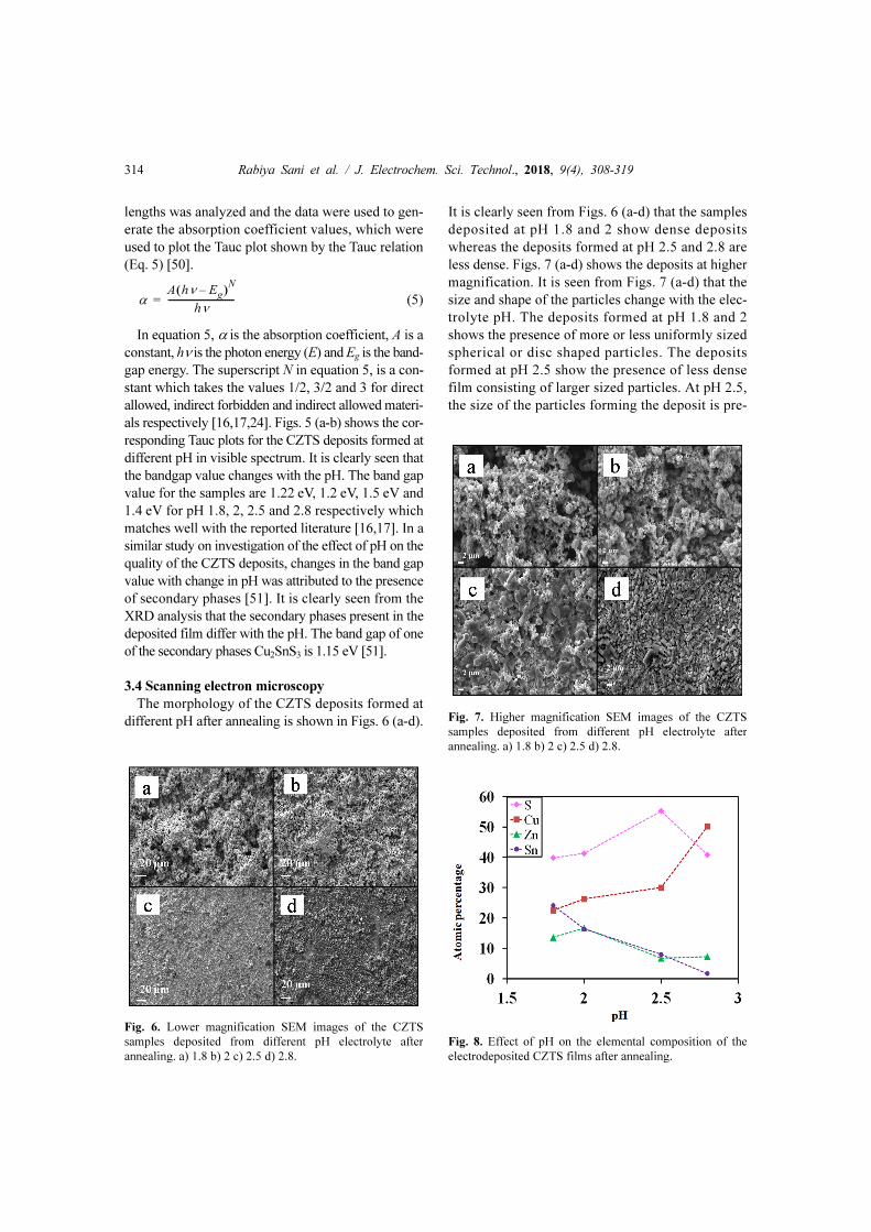
The morphology of the CZTS deposits formed atdifferent pH after annealing is shown in Figs. 6 (a-d).
It is clearly seen from Figs. 6 (a-d) that the samplesdeposited at pH 1.8 and 2 show dense depositswhereas the deposits formed at pH 2.5 and 2.8 areless dense. Figs. 7 (a-d) shows the deposits at highermagnification. It is seen from Figs. 7 (a-d) that thesize and shape of the particles change with the elec-trolyte pH. The deposits formed at pH 1.8 and 2shows the presence of more or less uniformly sizedspherical or disc shaped particles. The depositsformed at pH 2.5 show the presence of less densefilm consisting of larger sized particles. At pH 2.5,the size of the particles forming the deposit is pre-
αA hν Eg–( )
N
hν------------------------------=
Fig. 6. Lower magnification SEM images of the CZTS
samples deposited from different pH electrolyte after
annealing. a) 1.8 b) 2 c) 2.5 d) 2.8.
Fig. 7. Higher magnification SEM images of the CZTS
samples deposited from different pH electrolyte after
annealing. a) 1.8 b) 2 c) 2.5 d) 2.8.
Fig. 8. Effect of pH on the elemental composition of the
electrodeposited CZTS films after annealing.
Rabiya Sani et al. / J. Electrochem. Sci. Technol., 2018, 9(4), 308-319 315
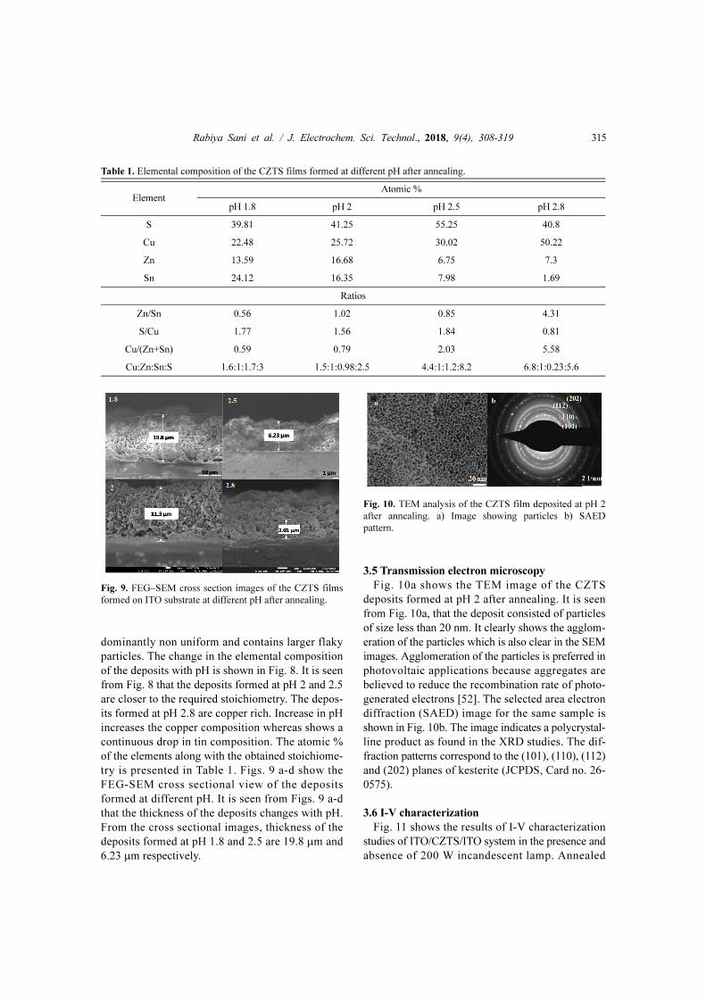
dominantly non uniform and contains larger flakyparticles. The change in the elemental compositionof the deposits with pH is shown in Fig. 8. It is seenfrom Fig. 8 that the deposits formed at pH 2 and 2.5are closer to the required stoichiometry. The depos-its formed at pH 2.8 are copper rich. Increase in pHincreases the copper composition whereas shows acontinuous drop in tin composition. The atomic %of the elements along with the obtained stoichiome-try is presented in Table 1. Figs. 9 a-d show theFEG-SEM cross sectional view of the depositsformed at different pH. It is seen from Figs. 9 a-dthat the thickness of the deposits changes with pH.From the cross sectional images, thickness of thedeposits formed at pH 1.8 and 2.5 are 19.8 µm and6.23 µm respectively.
3.5 Transmission electron microscopy
Fig. 10a shows the TEM image of the CZTSdeposits formed at pH 2 after annealing. It is seenfrom Fig. 10a, that the deposit consisted of particlesof size less than 20 nm. It clearly shows the agglom-eration of the particles which is also clear in the SEMimages. Agglomeration of the particles is preferred inphotovoltaic applications because aggregates arebelieved to reduce the recombination rate of photo-generated electrons [52]. The selected area electrondiffraction (SAED) image for the same sample isshown in Fig. 10b. The image indicates a polycrystal-line product as found in the XRD studies. The dif-fraction patterns correspond to the (101), (110), (112)and (202) planes of kesterite (JCPDS, Card no. 26-0575).
3.6 I-V characterization
Fig. 11 shows the results of I-V characterizationstudies of ITO/CZTS/ITO system in the presence andabsence of 200 W incandescent lamp. Annealed
Table 1. Elemental composition of the CZTS films formed at different pH after annealing.
ElementAtomic %
pH 1.8 pH 2 pH 2.5 pH 2.8
S 39.81 41.25 55.25 40.8
Cu 22.48 25.72 30.02 50.22
Zn 13.59 16.68 6.75 7.3
Sn 24.12 16.35 7.98 1.69
Ratios
Zn/Sn 0.56 1.02 0.85 4.31
S/Cu 1.77 1.56 1.84 0.81
Cu/(Zn+Sn) 0.59 0.79 2.03 5.58
Cu:Zn:Sn:S 1.6:1:1.7:3 1.5:1:0.98:2.5 4.4:1:1.2:8.2 6.8:1:0.23:5.6
Fig. 9. FEG–SEM cross section images of the CZTS films
formed on ITO substrate at different pH after annealing.
Fig. 10. TEM analysis of the CZTS film deposited at pH 2
after annealing. a) Image showing particles b) SAED
pattern.
316 Rabiya Sani et al. / J. Electrochem. Sci. Technol., 2018, 9(4), 308-319
CZTS deposits were used in the studies. The I-Vcharacterization studies give a straight line pattern inthe potential range studied. Such a straight line fea-ture indicates the Ohmic nature of the system [50].The slope of the line decreases in the presence oflight which shows that the deposit is suitable for solarcell applications [50]. The resistance values in theabsence of light for the samples deposited at pH 2.5and 2.8 are ten times higher than the resistance valuesin the presence of light source. The resistance valuesof the deposits in the presence and absence of lightare shown in Table 2. The sample synthesized at pH
1.8 though deviates slightly from the stoichiometry,gives low resistance value when compared to othersamples which could be due to the difference in thethickness of the deposits as observed from SEMimages. The significant drop in the resistance valuesin the presence of light source clearly indicates thesuitability of the synthesized deposits for solar cellabsorber material. In a study on the electrodepositionof CZTS on FTO substrate using trisodium citrate asthe complexing agent, deposits having electrical con-ductance of 52 µS were synthesized [51]. The electri-cal conductance values of the CZTS depositssynthesized in this report are in the range of 9 mS to33 mS in the presence of light. Thus, the deposits aresuitable for solar cell applications.
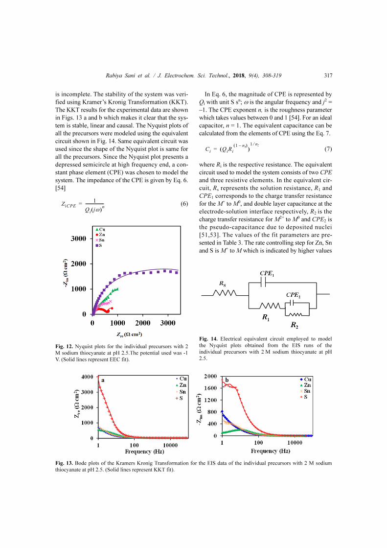
3.7 Electrochemical impedance spectroscopy
Fig. 12 shows the Nyquist plots for the individualprecursors with the complexing agent at pH 2.5. TheNyquist plot presents a depressed semicircle in thehigh frequency range which could be attributed tofrequency dispersion due to surface inhomogeneity[53]. The low frequency end of the Nyquist plot forall the precursors presents a larger semicircle which
Fig. 11. I-V characteristic patterns of the CZTS samples deposited from different pH electrolyte in the presence and in the
absence of light after annealing. (Solid lines show the response of the deposit in light, dotted lines in dark)
Table 2. Resistance values from the I-V characterization
studies of the annealed CZTS films deposited at different
pH in the presence and absence of light.
Resistance / Ω
pH Light Dark
1.8 32 123
2 83 188
2.5 110 1400
2.8 68 500
Rabiya Sani et al. / J. Electrochem. Sci. Technol., 2018, 9(4), 308-319 317
is incomplete. The stability of the system was veri-fied using Kramer’s Kronig Transformation (KKT).The KKT results for the experimental data are shownin Figs. 13 a and b which makes it clear that the sys-tem is stable, linear and causal. The Nyquist plots ofall the precursors were modeled using the equivalentcircuit shown in Fig. 14. Same equivalent circuit wasused since the shape of the Nyquist plot is same forall the precursors. Since the Nyquist plot presents adepressed semicircle at high frequency end, a con-stant phase element (CPE) was chosen to model thesystem. The impedance of the CPE is given by Eq. 6.[54]
(6)
In Eq. 6, the magnitude of CPE is represented byQi with unit S sn; ω is the angular frequency and j2 =–1. The CPE exponent n, is the roughness parameterwhich takes values between 0 and 1 [54]. For an idealcapacitor, n = 1. The equivalent capacitance can becalculated from the elements of CPE using the Eq. 7.
(7)
where Ri is the respective resistance. The equivalentcircuit used to model the system consists of two CPE
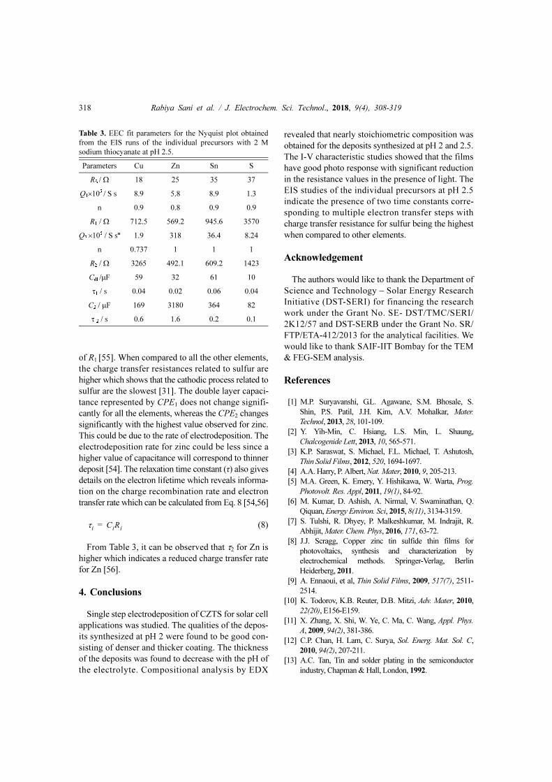
and three resistive elements. In the equivalent cir-cuit, Rs represents the solution resistance, R1 andCPE1 corresponds to the charge transfer resistancefor the M+ to M0, and double layer capacitance at theelectrode-solution interface respectively, R2 is thecharge transfer resistance for M2+ to M0 and CPE2 isthe pseudo-capacitance due to deposited nuclei[51,53]. The values of the fit parameters are pre-sented in Table 3. The rate controlling step for Zn, Snand S is M+ to M which is indicated by higher values
ZiCPE
1
Qi jω( )n
-------------------=
Ci QiRi
1 ni
–( )( )
1 ni
⁄
=
Fig. 12. Nyquist plots for the individual precursors with 2
M sodium thiocyanate at pH 2.5.The potential used was -1
V. (Solid lines represent EEC fit).
Fig. 13. Bode plots of the Kramers Kronig Transformation for the EIS data of the individual precursors with 2 M sodium
thiocyanate at pH 2.5. (Solid lines represent KKT fit).
Fig. 14. Electrical equivalent circuit employed to model
the Nyquist plots obtained from the EIS runs of the
individual precursors with 2 M sodium thiocyanate at pH
2.5.
318 Rabiya Sani et al. / J. Electrochem. Sci. Technol., 2018, 9(4), 308-319
of R1 [55]. When compared to all the other elements,the charge transfer resistances related to sulfur arehigher which shows that the cathodic process related tosulfur are the slowest [31]. The double layer capaci-tance represented by CPE1 does not change signifi-cantly for all the elements, whereas the CPE2 changessignificantly with the highest value observed for zinc.This could be due to the rate of electrodeposition. Theelectrodeposition rate for zinc could be less since ahigher value of capacitance will correspond to thinnerdeposit [54]. The relaxation time constant (τ) also givesdetails on the electron lifetime which reveals informa-tion on the charge recombination rate and electrontransfer rate which can be calculated from Eq. 8 [54,56]
(8)
From Table 3, it can be observed that τ2 for Zn ishigher which indicates a reduced charge transfer ratefor Zn [56].
4. Conclusions
Single step electrodeposition of CZTS for solar cellapplications was studied. The qualities of the depos-its synthesized at pH 2 were found to be good con-sisting of denser and thicker coating. The thicknessof the deposits was found to decrease with the pH ofthe electrolyte. Compositional analysis by EDX
revealed that nearly stoichiometric composition wasobtained for the deposits synthesized at pH 2 and 2.5.The I-V characteristic studies showed that the filmshave good photo response with significant reductionin the resistance values in the presence of light. TheEIS studies of the individual precursors at pH 2.5indicate the presence of two time constants corre-sponding to multiple electron transfer steps withcharge transfer resistance for sulfur being the highestwhen compared to other elements.
Acknowledgement
The authors would like to thank the Department ofScience and Technology – Solar Energy ResearchInitiative (DST-SERI) for financing the researchwork under the Grant No. SE- DST/TMC/SERI/2K12/57 and DST-SERB under the Grant No. SR/FTP/ETA-412/2013 for the analytical facilities. Wewould like to thank SAIF-IIT Bombay for the TEM& FEG-SEM analysis.
References
[1] M.P. Suryavanshi, G.L. Agawane, S.M. Bhosale, S.
Shin, P.S. Patil, J.H. Kim, A.V. Mohalkar, Mater.
Technol, 2013, 28, 101-109.
[2] Y. Yih-Min, C. Hsiang, L.S. Min, L. Shaung,
Chalcogenide Lett, 2013, 10, 565-571.
[3] K.P. Saraswat, S. Michael, F.L. Michael, T. Ashutosh,
Thin Solid Films, 2012, 520, 1694-1697.
[4] A.A. Harry, P. Albert, Nat. Mater, 2010, 9, 205-213.
[5] M.A. Green, K. Emery, Y. Hishikawa, W. Warta, Prog.
Photovolt. Res. Appl, 2011, 19(1), 84-92.
[6] M. Kumar, D. Ashish, A. Nirmal, V. Swaminathan, Q.
Qiquan, Energy Environ. Sci, 2015, 8(11), 3134-3159.
[7] S. Tulshi, R. Dhyey, P. Malkeshkumar, M. Indrajit, R.
Abhijit, Mater. Chem. Phys, 2016, 171, 63-72.
[8] J.J. Scragg, Copper zinc tin sulfide thin films for
photovoltaics, synthesis and characterization by
electrochemical methods. Springer-Verlag, Berlin
Heiderberg, 2011.
[9] A. Ennaoui, et al, Thin Solid Films, 2009, 517(7), 2511-
2514.
[10] K. Todorov, K.B. Reuter, D.B. Mitzi, Adv. Mater, 2010,
22(20), E156-E159.
[11] X. Zhang, X. Shi, W. Ye, C. Ma, C. Wang, Appl. Phys.
A, 2009, 94(2), 381-386.
[12] C.P. Chan, H. Lam, C. Surya, Sol. Energ. Mat. Sol. C,
2010, 94(2), 207-211.
[13] A.C. Tan, Tin and solder plating in the semiconductor
industry, Chapman & Hall, London, 1992.
τi CiRi=
Table 3. EEC fit parameters for the Nyquist plot obtained
from the EIS runs of the individual precursors with 2 M
sodium thiocyanate at pH 2.5.
Parameters Cu Zn Sn S
RS / Ω 18 25 35 37
Q1×105 / S sn 8.9 5.8 8.9 1.3
n 0.9 0.8 0.9 0.9
R1 / Ω 712.5 569.2 945.6 3570
Q2 ×105 / S sn 1.9 318 36.4 8.24
n 0.737 1 1 1
R2 / Ω 3265 492.1 609.2 1423
Cdl /μF 59 32 61 10
τ1 / s 0.04 0.02 0.06 0.04
C2 / μF 169 3180 364 82
τ 2 / s 0.6 1.6 0.2 0.1
Rabiya Sani et al. / J. Electrochem. Sci. Technol., 2018, 9(4), 308-319 319
[14] C.Y. Sheng, W.Y. Jun, L. Rui, G.J. Hua, L.J. Xiao, Y.
Shi, Chin. Phys. B, 2012, 21, 058801-04.
[15] S. Ahmed, K.B. Reuter, O. Gunawan, L. Guo, L.T.
Romankiw, H. Deligianni, Adv. Energ. Mater, 2012,
2(2), 253-259.
[16] B.S. Pawar, S.M. Pawar, S.W. Shin, D.S. Choi, C.J.
Park, S.S. Kolekar, J.H. Kim, Appl. Surf. Sci, 2010,
257(5), 1786-1791.
[17] S.M. Pawar, B.S. Pawar, A.V. Moholkar, D.S. Choi, J.H.
Yun, J.H. Moon, Electrochim. Acta , 2010, 55(12), 4057-
4061.
[18] J.H. Lee, H.J. Choi, W.M. Kim, J.H. Jeong, J.K. Park,
Solar Energy, 2016, 136, 499-504.
[19] A. Emrani, P. Vasekar, C.R. Westgate, Solar Energy,
2013, 98, 335-340.
[20] H. Zhang, S. Cheng, J. Yu, Y. Lai, H. Zhou, H. Jia, ECS
J. Solid State Sci. Technol, 2016, 5(9), P521-P525.
[21] J.J.M. Josiah, D.H. Rasmussen, I.I. Suni, J. Electrochem.
Soc, 2011, 158(2), D54-D56.
[22] R.Sani, R. Manivannan, S.N. Victoria, Chal. Lett, 2017,
14,165-170.
[23] M.G. Ganchev, K.D. Kochev, Sol. Energ. Mat. Sol.
Cells, 1993, 31(2), 163-170.
[24] S.B. Pawar, M.S. Pawar, V.K. Gurav, W.S. Shin, Y.J.
Lee, S.S. Kolekar, H.J. Kim, ISRN Renewable Energy,
2011, 934575.
[25] M. Farinella, R. Inguanta, T. Spanio, P. Livreri, S.
Piazza, C. Sunseri, Energy Proceedia, 2013, 44,105-110.
[26] D. Pletcher, Industrial electrochemistry, Springer Science
+ Business Media, B.V, 1984.
[27] A. Brenner, Electrodeposition of alloys principles and
practice, Vol. 1, Academic Press, New York, 1963.
[28] N. Touabi, S. Martinez, M. Bounoughaz, Int. J.
Electrochem. Sci, 2015, 10, 7227-7240.
[29] K. Marianna, M. Ritala, H. Saloniemi, M. Leskelä, T.
Sajavaara, E. Rauhalab, J. Electrochem. Soc, 147, 2000,
147(3), 1080-1087.
[30] S. Arratia, H.A. Meneses, R.S. Guzman, C.C. Jara, Lat.
Am. Appl. Res, 2012, 42(4), 371-376.
[31] J.U. Emmanuel, I.A. Udoetok, N.W. Akpanudo, IOSR J.
Appl. Chem, 2013, 5, 50-55.
[32] A. Tang, Z. Li, F. Wang, M. Dou, Y. Pan, J. Guan, Appl.
Surf. Sci, 2017, 402, 70-77.
[33] X. Xu, F. Wang, Z. Li, J. Liu, J. Ji, J. Chen, Electrochim.
Acta, 2013, 87, 511-517.
[34] T. Fuchigami, S. Inagi, M. Atobe, Fundamentals and
applications of organic electrochemistry, John Wiley &
Sons, United Kingdom, 2014.
[35] W.D. Shahizuan, Y. Mohd, J. Sci. Technol, 2012, 4(1),
49-60.
[36] A. Ullah, A. Rauf, U.A. Rana, R. Qureshi, M.N. Ashiq,
H. Hussain, H.-B. Kraatz, A. Badshah, A. Shah, J.
Electrochem. Soc, 2015, 162(3), H157-H163.
[37] A.A. Akl, A.S. Hassanien, Int. J. Adv. Res, 2014, 2(11),
1-9.
[38] L. Choubrac, A. Lafond, C. Guillot-Deudon, Y. Moelo,
S. Jobic, Inorg. Chem, 2012, 51(6), 3346-3348.
[39] J.L. van Heerden, R. Swanepoel, Thin Solid Films,
1997, 299(12), 72-77.
[40] M. Li, W.H. Zhou, J. Guo, Y.L. Zhou, Z.L. Hou, J. Jiao,
Z.J. Zhou, Z.L. Du, S.X. Wu, J. Phys. Chem. C, 2012,
116(50), 26507-26516.
[41] M.C. Sekou, L. Wang, X. Zhang, Nanotechnology,
2013, 24, 495401-495410.
[42] D.K. Kaushik, T.N.Rao, A.Subrahmanyam, Surf. Coat.
Tech, 2017, 314, 85-91.
[43] S.B. Arvid, B. Marsen, S. Cinque, U. Thomas, K.
Reiner, S. Schorr, H.W. Schock, Prog. Photovolt.: Res.
Appl, 2011, 19(1), 93-96.
[44] A.J. Cheng, M. Manno, A. Khare, C. Leighton, S.A.
Campbell, E.S. Aydil, J. Vac. Sci. Technol. A: Vacuum,
Surfaces, and Films, 2011, 29(5), 051203.
[45] C. Ivan, B. Ester, M. Rafael, F. Diego, L.T. Stoyanova,
C.B. Juan, Boletín de la Sociedad Española de
Cerámica y Vidrio, 2015, 54(5), 175-180.
[46] M.N. Shinde, P.D. Dubal, S.D. Dhawale, D.C.
Lokhande, H.J. Kim, H.J. Moon, Mater. Res. Bull, 2012,
47(2), 302-307.
[47] F. Aslan, A. Goktas, A. Tumbul, Mater. Sci. Semicon.
Process, 2016, 43, 139-143.
[48] S. Islam, M.A. Hossain, H. Kabir, M. Rahaman, M.S.
Bashar, M.A. Gafur, A. Kabir, M.M.R. Bhuiyan, F.
Ahmed, N. Khatun, Int. J. Thin Film Sci. Tecnol, 2015,
3,155-161.
[49] H. Suarez, J.M. Correa, S.D. Cruz, C.A. Otalora, M.
Hurtado, G. Gordillo, IEEE Transactions, 2013, 2585-
2589.
[50] S. Alok, R. Manivannan, S.N. Victoria, Arabian J. Chem,
2015.
[51] B. Ananthoju, A. Kushwaha, F.J. Sonia, M. Aslam, AIP
Conf. Proc., 2013, 1512, 706.
[52] S.M. Camara, L. Wang, X. Zhang, Nanotechnology,
2013, 24, 495401.
[53] S.N. Victoria, R. Prasad, R. Manivannan, Int. J.
Electrochem. Sci, 2015, 10, 2220-2238.
[54] B.S. Swaroop, S.N. Victoria, R. Manivannan, J. Taiwan
Inst. Chem. Eng, 2016, 64, 269-278.
[55] V. Gerardo, C.M. Fernández, I. Gonazález, ECS Trans,
2008, 15(1), 171-180.
[56] Z. Xinwei, H. Fan, Y. Tian, M. Zhang, X. Yan, RSC
Adv, 2015, 5(30), 23401-23409.