Embed Size (px)
Citation preview
Frequency (Hz)
116
106
96
86
76
66
100k 1M 10M 50M
Tra
nsim
pedance G
ain
(dB
)
10MHz Bandwidth
OPA657(12pF)
l
-Vb
200kΩ
VO
0.1pF
Product
Folder
Sample &Buy
Technical
Documents
Tools &
Software
Support &Community
OPA657SBOS197F –DECEMBER 2001–REVISED AUGUST 2015
OPA657 1.6-GHz, Low-Noise, FET-Input Operational Amplifier1 Features 3 Description
The OPA657 device combines a high-gain bandwidth,1• High Gain Bandwidth Product: 1.6 GHz
low-distortion, voltage-feedback operational amplifier• High Bandwidth 275 MHz (G = 10) with a low-voltage noise JFET-input stage to offer a• Slew Rate 700 V/µs (G = 10, 1-V Step) very high dynamic range amplifier for high-precision
ADC (analog-to-digital converter) driving or wideband• Available in High Grade With Improved DCtransimpedance applications. Photodiode applicationsSpecificationssee improved noise and bandwidth using this• Operating Temperature Range: –40°C to 85°C decompensated, high-gain bandwidth amplifier.
• Low-Input Offset Voltage: ±250 µVVery low level signals can be significantly amplified in• Low-Input Bias Current: 2 pA a single OPA657 gain stage with exceptional
• Low-Input Voltage Noise: 4.8 nV/√Hz bandwidth and accuracy. Having a high 1.6-GHz gainbandwidth product gives greater than 10-MHz signal• High-Output Current: 70 mAbandwidths up to gains of 160 V/V (44 dB). The very• Fast Overdrive Recovery low input bias current and capacitance supports thisperformance even for relatively high source2 Applications impedances.
• Wideband Photodiode Amplifier Broadband photodetector applications benefit from• Wafer Scanning Equipment the low-voltage noise JFET inputs for the OPA657.
The JFET input contributes virtually no current noise• ADC Input Amplifierwhile for broadband applications, a low voltage noise• Test and Measurement Front End is also required. The low 4.8 nV/√Hz input voltage
• High Gain Precision Amplifier noise provides exceptional input sensitivity for higherbandwidth applications. The example shown below• Optical Time Domain Reflectometry (OTDR)gives a total equivalent input noise current of 1.8pA/√Hz over a 10-MHz bandwidth.
Device Information(1)
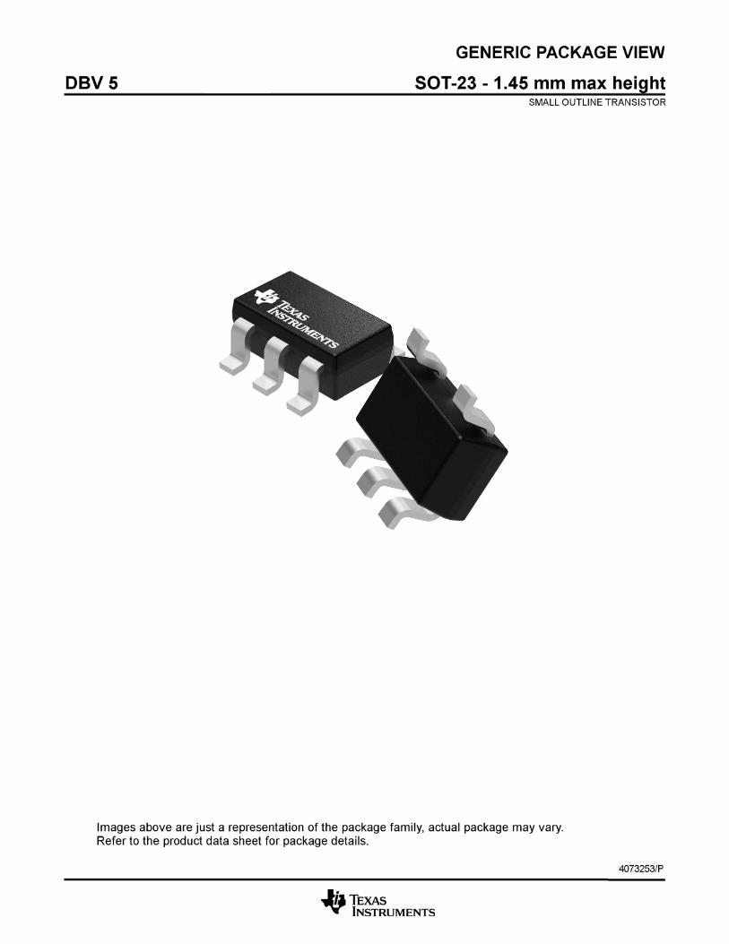
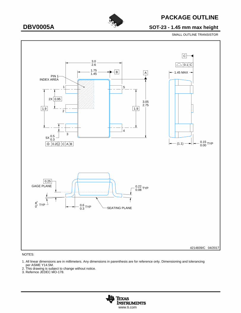
PART NUMBER PACKAGE BODY SIZE (NOM)SOT-23 (5) 2.90 mm × 1.60 mm
OPA657SOIC (8) 4.90 mm × 3.91 mm
(1) For all available packages, see the orderable addendum atthe end of the data sheet.
Frequency Response of 200-kΩ TransimpedanceWideband Photodiode Transimpedance AmplifierAmplifier
1
An IMPORTANT NOTICE at the end of this data sheet addresses availability, warranty, changes, use in safety-critical applications,intellectual property matters and other important disclaimers. PRODUCTION DATA.
OPA657SBOS197F –DECEMBER 2001–REVISED AUGUST 2015 www.ti.com
Table of Contents8.2 Feature Description................................................. 131 Features .................................................................. 18.3 Device Functional Modes........................................ 132 Applications ........................................................... 1
9 Application and Implementation ........................ 143 Description ............................................................. 19.1 Application Information............................................ 144 Revision History..................................................... 29.2 Typical Application .................................................. 215 Related Operational Amplifier Products.............. 3
10 Power Supply Recommendations ..................... 246 Pin Configuration and Functions ......................... 311 Layout................................................................... 247 Specifications......................................................... 4
11.1 Layout Guidelines ................................................. 247.1 Absolute Maximum Ratings ...................................... 411.2 Layout Example .................................................... 267.2 ESD Ratings.............................................................. 411.3 Thermal Considerations ........................................ 267.3 Recommended Operating Conditions....................... 4
12 Device and Documentation Support ................. 287.4 Thermal Information .................................................. 412.1 Community Resources.......................................... 287.5 Electrical Characteristics: VS = ±5 V......................... 512.2 Trademarks ........................................................... 287.6 Electrical Characteristics: VS - ±5 V, High-Grade DC12.3 Electrostatic Discharge Caution............................ 28Specifications ............................................................. 712.4 Glossary ................................................................ 287.7 Typical Characteristics: VS = ±5 V............................ 8
13 Mechanical, Packaging, and Orderable8 Detailed Description ............................................ 13Information ........................................................... 288.1 Overview ................................................................. 13
4 Revision HistoryNOTE: Page numbers for previous revisions may differ from page numbers in the current version.
Changes from Revision E (December 2008) to Revision F Page
• Added ESD Ratings table, Feature Description section, Device Functional Modes, Application and Implementationsection, Power Supply Recommendations section, Layout section, Device and Documentation Support section, andMechanical, Packaging, and Orderable Information section ................................................................................................. 1
• Deleted lead temperature parameter from Absolute Maximum Ratings table ....................................................................... 4• Added Power Supply, Minimum Operating Voltage specification to ±5V Electrical Characteristics table ............................. 6
Changes from Revision D (March 2006) to Revision E Page
• Changed minimum storage temperature range from –40°C to –65°C ................................................................................... 4
2 Submit Documentation Feedback Copyright © 2001–2015, Texas Instruments Incorporated
Product Folder Links: OPA657
1
2
3
5
4
+VS
VIN–
VOUT
-VS
VIN+
A57
15 4
Pin Orientation/Package Marking
2 3
1
2
3
4
8
7
6
5
NC
+VS
VOUT
NC
NC
VIN–
VIN+
-VS
OPA657www.ti.com SBOS197F –DECEMBER 2001–REVISED AUGUST 2015
5 Related Operational Amplifier Products
SLEW RATE VOLTAGE NOISEDEVICE VS (V) BW (MHz) (V/μs) (nV/√Hz) AMPLIFIER DESCRIPTIONOPA657 ±5 1600 700 4.8 Gain of +7 stable FET InputOPA656 ±5 230 290 7 Unity-Gain Stable FET-InputOPA659 ±6 350 2550 8.9 Unity-Gain Stable FET-InputLMH6629 5 4000 1600 0.69 Gain of +10 stable Bipolar InputTHS4631 ±15 210 1000 7 Unity-Gain Stable FET-Input
Programmable Gain (5 kΩ / 20 kΩ)OPA857 5 4750 220 — Transimpedance Amplifier
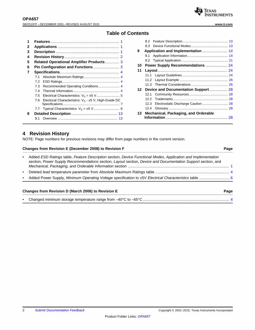
6 Pin Configuration and Functions
D PackageDBV Package8-Pin SOIC Surface-Mount5-Pin SOT-23Top View
Top View
Pin FunctionsPIN
I/O DESCRIPTIONNAME SOIC SOT-23
1NC 5 — — No Connection
8VIN– 2 4 I Inverting InputVIN+ 3 3 I Noninverting Input–VS 4 2 POW Negative Power SupplyVOUT 6 1 O Output of amplifier+VS 7 5 POW Positive Power Supply
Copyright © 2001–2015, Texas Instruments Incorporated Submit Documentation Feedback 3
Product Folder Links: OPA657
OPA657SBOS197F –DECEMBER 2001–REVISED AUGUST 2015 www.ti.com
7 Specifications
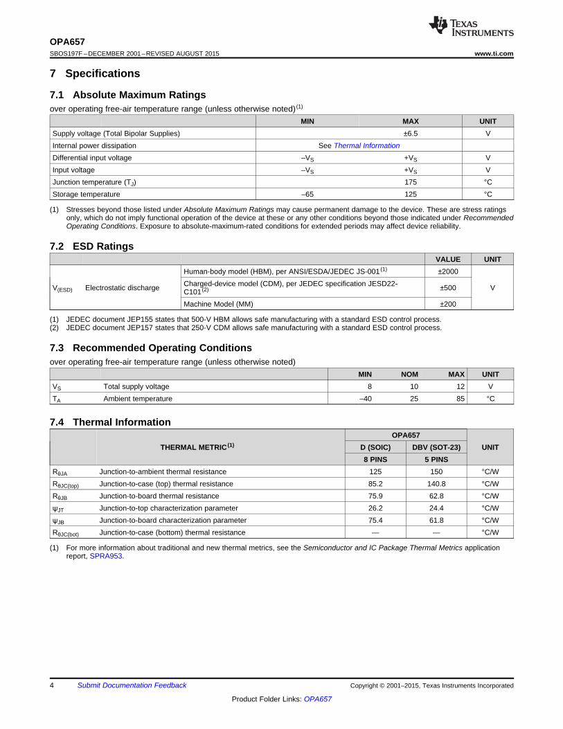
7.1 Absolute Maximum Ratingsover operating free-air temperature range (unless otherwise noted) (1)
MIN MAX UNITSupply voltage (Total Bipolar Supplies) ±6.5 VInternal power dissipation See Thermal InformationDifferential input voltage –VS +VS VInput voltage –VS +VS VJunction temperature (TJ) 175 °CStorage temperature –65 125 °C
(1) Stresses beyond those listed under Absolute Maximum Ratings may cause permanent damage to the device. These are stress ratingsonly, which do not imply functional operation of the device at these or any other conditions beyond those indicated under RecommendedOperating Conditions. Exposure to absolute-maximum-rated conditions for extended periods may affect device reliability.
7.2 ESD RatingsVALUE UNIT
Human-body model (HBM), per ANSI/ESDA/JEDEC JS-001 (1) ±2000Charged-device model (CDM), per JEDEC specification JESD22-V(ESD) Electrostatic discharge ±500 VC101 (2)
Machine Model (MM) ±200
(1) JEDEC document JEP155 states that 500-V HBM allows safe manufacturing with a standard ESD control process.(2) JEDEC document JEP157 states that 250-V CDM allows safe manufacturing with a standard ESD control process.
7.3 Recommended Operating Conditionsover operating free-air temperature range (unless otherwise noted)
MIN NOM MAX UNITVS Total supply voltage 8 10 12 VTA Ambient temperature –40 25 85 °C
7.4 Thermal InformationOPA657
THERMAL METRIC (1) D (SOIC) DBV (SOT-23) UNIT8 PINS 5 PINS
RθJA Junction-to-ambient thermal resistance 125 150 °C/WRθJC(top) Junction-to-case (top) thermal resistance 85.2 140.8 °C/WRθJB Junction-to-board thermal resistance 75.9 62.8 °C/WψJT Junction-to-top characterization parameter 26.2 24.4 °C/WψJB Junction-to-board characterization parameter 75.4 61.8 °C/WRθJC(bot) Junction-to-case (bottom) thermal resistance — — °C/W
(1) For more information about traditional and new thermal metrics, see the Semiconductor and IC Package Thermal Metrics applicationreport, SPRA953.
4 Submit Documentation Feedback Copyright © 2001–2015, Texas Instruments Incorporated
Product Folder Links: OPA657
OPA657www.ti.com SBOS197F –DECEMBER 2001–REVISED AUGUST 2015
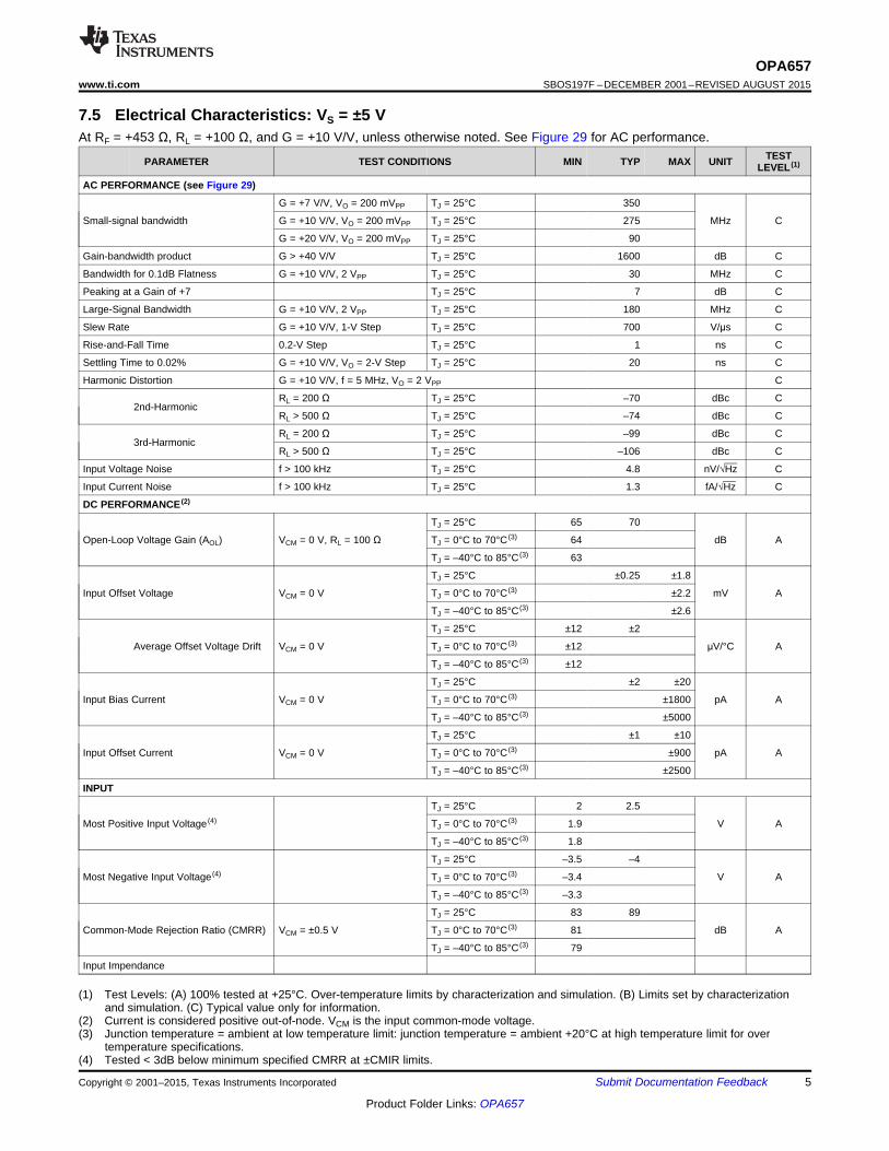
7.5 Electrical Characteristics: VS = ±5 VAt RF = +453 Ω, RL = +100 Ω, and G = +10 V/V, unless otherwise noted. See Figure 29 for AC performance.
TESTPARAMETER TEST CONDITIONS MIN TYP MAX UNIT LEVEL (1)
AC PERFORMANCE (see Figure 29)
G = +7 V/V, VO = 200 mVPP TJ = 25°C 350
Small-signal bandwidth G = +10 V/V, VO = 200 mVPP TJ = 25°C 275 MHz C
G = +20 V/V, VO = 200 mVPP TJ = 25°C 90
Gain-bandwidth product G > +40 V/V TJ = 25°C 1600 dB C
Bandwidth for 0.1dB Flatness G = +10 V/V, 2 VPP TJ = 25°C 30 MHz C
Peaking at a Gain of +7 TJ = 25°C 7 dB C
Large-Signal Bandwidth G = +10 V/V, 2 VPP TJ = 25°C 180 MHz C
Slew Rate G = +10 V/V, 1-V Step TJ = 25°C 700 V/μs C
Rise-and-Fall Time 0.2-V Step TJ = 25°C 1 ns C
Settling Time to 0.02% G = +10 V/V, VO = 2-V Step TJ = 25°C 20 ns C
Harmonic Distortion G = +10 V/V, f = 5 MHz, VO = 2 VPP C
RL = 200 Ω TJ = 25°C –70 dBc C2nd-Harmonic
RL > 500 Ω TJ = 25°C –74 dBc C
RL = 200 Ω TJ = 25°C –99 dBc C3rd-Harmonic
RL > 500 Ω TJ = 25°C –106 dBc C
Input Voltage Noise f > 100 kHz TJ = 25°C 4.8 nV/√Hz C
Input Current Noise f > 100 kHz TJ = 25°C 1.3 fA/√Hz C
DC PERFORMANCE (2)
TJ = 25°C 65 70
Open-Loop Voltage Gain (AOL) VCM = 0 V, RL = 100 Ω TJ = 0°C to 70°C (3) 64 dB A
TJ = –40°C to 85°C (3) 63
TJ = 25°C ±0.25 ±1.8
Input Offset Voltage VCM = 0 V TJ = 0°C to 70°C (3) ±2.2 mV A
TJ = –40°C to 85°C (3) ±2.6
TJ = 25°C ±12 ±2
Average Offset Voltage Drift VCM = 0 V TJ = 0°C to 70°C (3) ±12 μV/°C A
TJ = –40°C to 85°C (3) ±12
TJ = 25°C ±2 ±20
Input Bias Current VCM = 0 V TJ = 0°C to 70°C (3) ±1800 pA A
TJ = –40°C to 85°C (3) ±5000
TJ = 25°C ±1 ±10
Input Offset Current VCM = 0 V TJ = 0°C to 70°C (3) ±900 pA A
TJ = –40°C to 85°C (3) ±2500
INPUT
TJ = 25°C 2 2.5
Most Positive Input Voltage (4) TJ = 0°C to 70°C (3) 1.9 V A
TJ = –40°C to 85°C (3) 1.8
TJ = 25°C –3.5 –4
Most Negative Input Voltage (4) TJ = 0°C to 70°C (3) –3.4 V A
TJ = –40°C to 85°C (3) –3.3
TJ = 25°C 83 89
Common-Mode Rejection Ratio (CMRR) VCM = ±0.5 V TJ = 0°C to 70°C (3) 81 dB A
TJ = –40°C to 85°C (3) 79
Input Impendance
(1) Test Levels: (A) 100% tested at +25°C. Over-temperature limits by characterization and simulation. (B) Limits set by characterizationand simulation. (C) Typical value only for information.
(2) Current is considered positive out-of-node. VCM is the input common-mode voltage.(3) Junction temperature = ambient at low temperature limit: junction temperature = ambient +20°C at high temperature limit for over
temperature specifications.(4) Tested < 3dB below minimum specified CMRR at ±CMIR limits.
Copyright © 2001–2015, Texas Instruments Incorporated Submit Documentation Feedback 5
Product Folder Links: OPA657
OPA657SBOS197F –DECEMBER 2001–REVISED AUGUST 2015 www.ti.com
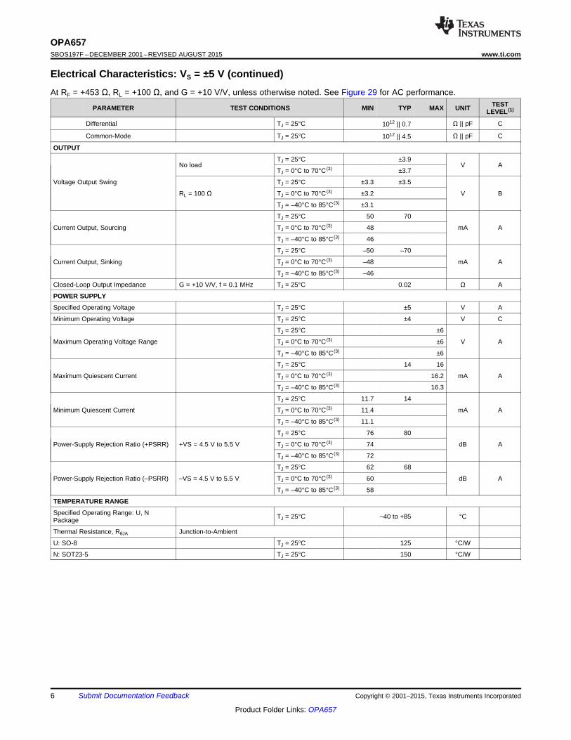
Electrical Characteristics: VS = ±5 V (continued)At RF = +453 Ω, RL = +100 Ω, and G = +10 V/V, unless otherwise noted. See Figure 29 for AC performance.
TESTPARAMETER TEST CONDITIONS MIN TYP MAX UNIT LEVEL (1)
Differential TJ = 25°C Ω || pF C1012 || 0.7
Common-Mode TJ = 25°C Ω || pF C1012 || 4.5
OUTPUT
TJ = 25°C ±3.9No load V A
TJ = 0°C to 70°C (3) ±3.7
Voltage Output Swing TJ = 25°C ±3.3 ±3.5
RL = 100 Ω TJ = 0°C to 70°C (3) ±3.2 V B
TJ = –40°C to 85°C (3) ±3.1
TJ = 25°C 50 70
Current Output, Sourcing TJ = 0°C to 70°C (3) 48 mA A
TJ = –40°C to 85°C (3) 46
TJ = 25°C –50 –70
Current Output, Sinking TJ = 0°C to 70°C (3) –48 mA A
TJ = –40°C to 85°C (3) –46
Closed-Loop Output Impedance G = +10 V/V, f = 0.1 MHz TJ = 25°C 0.02 Ω A
POWER SUPPLY
Specified Operating Voltage TJ = 25°C ±5 V A
Minimum Operating Voltage TJ = 25°C ±4 V C
TJ = 25°C ±6
Maximum Operating Voltage Range TJ = 0°C to 70°C (3) ±6 V A
TJ = –40°C to 85°C (3) ±6
TJ = 25°C 14 16
Maximum Quiescent Current TJ = 0°C to 70°C (3) 16.2 mA A
TJ = –40°C to 85°C (3) 16.3
TJ = 25°C 11.7 14
Minimum Quiescent Current TJ = 0°C to 70°C (3) 11.4 mA A
TJ = –40°C to 85°C (3) 11.1
TJ = 25°C 76 80
Power-Supply Rejection Ratio (+PSRR) +VS = 4.5 V to 5.5 V TJ = 0°C to 70°C (3) 74 dB A
TJ = –40°C to 85°C (3) 72
TJ = 25°C 62 68
Power-Supply Rejection Ratio (–PSRR) –VS = 4.5 V to 5.5 V TJ = 0°C to 70°C (3) 60 dB A
TJ = –40°C to 85°C (3) 58
TEMPERATURE RANGE
Specified Operating Range: U, N TJ = 25°C –40 to +85 °CPackage
Thermal Resistance, RθJA Junction-to-Ambient
U: SO-8 TJ = 25°C 125 °C/W
N: SOT23-5 TJ = 25°C 150 °C/W
6 Submit Documentation Feedback Copyright © 2001–2015, Texas Instruments Incorporated
Product Folder Links: OPA657
OPA657www.ti.com SBOS197F –DECEMBER 2001–REVISED AUGUST 2015
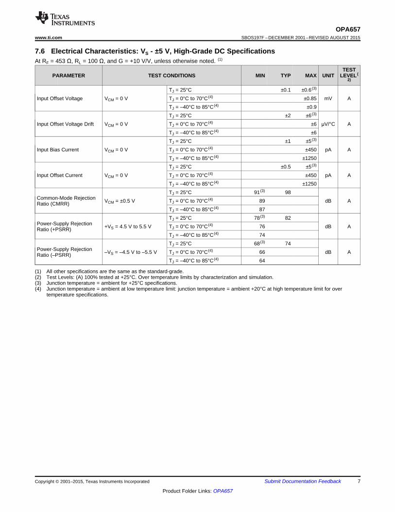
7.6 Electrical Characteristics: VS - ±5 V, High-Grade DC SpecificationsAt RF = 453 Ω, RL = 100 Ω, and G = +10 V/V, unless otherwise noted. (1)
TESTPARAMETER TEST CONDITIONS MIN TYP MAX UNIT LEVEL (
2)
TJ = 25°C ±0.1 ±0.6 (3)
Input Offset Voltage VCM = 0 V TJ = 0°C to 70°C (4) ±0.85 mV ATJ = –40°C to 85°C (4) ±0.9TJ = 25°C ±2 ±6 (3)
Input Offset Voltage Drift VCM = 0 V TJ = 0°C to 70°C (4) ±6 μV/°C ATJ = –40°C to 85°C (4) ±6TJ = 25°C ±1 ±5 (3)
Input Bias Current VCM = 0 V TJ = 0°C to 70°C (4) ±450 pA ATJ = –40°C to 85°C (4) ±1250TJ = 25°C ±0.5 ±5 (3)
Input Offset Current VCM = 0 V TJ = 0°C to 70°C (4) ±450 pA ATJ = –40°C to 85°C (4) ±1250TJ = 25°C 91 (3) 98
Common-Mode Rejection VCM = ±0.5 V TJ = 0°C to 70°C (4) 89 dB ARatio (CMRR)TJ = –40°C to 85°C (4) 87TJ = 25°C 78 (3) 82
Power-Supply Rejection +VS = 4.5 V to 5.5 V TJ = 0°C to 70°C (4) 76 dB ARatio (+PSRR)TJ = –40°C to 85°C (4) 74TJ = 25°C 68 (3) 74
Power-Supply Rejection –VS = –4.5 V to –5.5 V TJ = 0°C to 70°C (4) 66 dB ARatio (–PSRR)TJ = –40°C to 85°C (4) 64
(1) All other specifications are the same as the standard-grade.(2) Test Levels: (A) 100% tested at +25°C. Over temperature limits by characterization and simulation.(3) Junction temperature = ambient for +25°C specifications.(4) Junction temperature = ambient at low temperature limit: junction temperature = ambient +20°C at high temperature limit for over
temperature specifications.
Copyright © 2001–2015, Texas Instruments Incorporated Submit Documentation Feedback 7
Product Folder Links: OPA657
Time (10ns/div)
Sm
all-
Sig
na
l O
utp
ut
Vo
lta
ge
(2
00
mV
/div
) La
rge
-Sig
na
l Ou
tpu
t Vo
ltag
e (4
00m
V/d
iv)
0.8
0.6
0.4
0.2
0
-0.2
-0.4
-0.6
-0.8
1.6
1.2
0.8
0.4
0
-0.4
-0.8
-1.2
-1.6
Large-Signal Right Scale
Small-Signal Left Scale
See Figure 28
G = +10
Time (10ns/div)
Sm
all-
Sig
na
l O
utp
ut
Vo
lta
ge
(2
00
mV
/div
) La
rge
-Sig
na
l Ou
tpu
t Vo
ltag
e (4
00
mV
/div
)
0.8
0.6
0.4
0.2
0
-0.2
-0.4
-0.6
-0.8
1.6
1.2
0.8
0.4
0
-0.4
-0.8
-1.2
-1.6
Large-Signal Right Scale
Small-Signal Left Scale
See Figure 29
G = 20-
100.5 1 500100
Frequency (MHz)
Gain
(dB
)
26
23
20
17
14
11
8
5
2
-1
-4
See Figure 28
G = +10
V = 5VO PP
V = 2VO PP
V = 1VO PP
V = 0.2VO PP
100.5 1 500100
Frequency (MHz)
Gain
(dB
)
32
29
26
23
20
17
14
11
8
5
2
See Figure 29
G = 20-
R = 1kWF
V = 5VO PP
V = 1VO PP
V = 1VO PP
V = 0.2VO PP
100.5 1 500100
Frequency (MHz)
No
rma
lize
d G
ain
(d
B)
9
6
3
0
-3
-6
-9
-12
-15
-18
-21
See Figure 28
G = +20
G = +50
G = +10
V = 0.2VO PP
G = +7
100.5 1 500100
Frequency (MHz)
Norm
aliz
ed G
ain
(dB
)
9
6
3
0
-3
-6
-9
-12
-15
-18
-21
See Figure 29
V = 0.2VO PP
R = 50G W G = 12-
G = 20-
G = 50-
OPA657SBOS197F –DECEMBER 2001–REVISED AUGUST 2015 www.ti.com
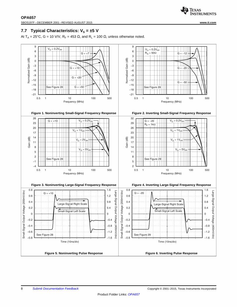
7.7 Typical Characteristics: VS = ±5 VAt TA = 25°C, G = 10 V/V, RF = 453 Ω, and RL = 100 Ω, unless otherwise noted.
Figure 1. Noninverting Small-Signal Frequency Response Figure 2. Inverting Small-Signal Frequency Response
Figure 3. Noninverting Large-Signal Frequency Response Figure 4. Inverting Large-Signal Frequency Response
Figure 5. Noninverting Pulse Response Figure 6. Inverting Pulse Response
8 Submit Documentation Feedback Copyright © 2001–2015, Texas Instruments Incorporated
Product Folder Links: OPA657
5 10 50
Gain (V/V)
Ha
rmo
nic
Dis
tort
ion
(d
Bc)
-40
-50
-60
-70
-80
-90
-100
-110
V = 2VO PP
f = 5MHz
R = 200WL
2nd Harmonic
3rd Harmonic
See Figure 28, R AdjustedG
10 50
Gain (V/V)
Ha
rmo
nic
Dis
tort
ion
(d
Bc)
-40
-50
-60
-70
-80
-90
-100
-110
V = 2VO PP
R = 50WG
f = 5MHz
R = 200WL
See Figure 29, R AdjustedF
2nd Harmonic
3rd Harmonic
0.5 1 5
Output Voltage Swing (V )PP
Ha
rmo
nic
Dis
tort
ion
(d
Bc)
-70
-75
-80
-85
-90
-95
-100
-105
-110
f = 1MHz
R = 200WL
See Figure 28
2nd Harmonic
3rd Harmonic
0.2 1 2010
Frequency (MHz)
Harm
onic
Dis
tort
ion (
dB
c)
-50
-60
-70
-80
-90
-100
-110
3rd Harmonic
2nd Harmonic
V = 2VO PP
R = 200WL
See Figure 28
0.5 1 5
Output Voltage Swing (V )PP
Ha
rmo
nic
Dis
tort
ion
(d
Bc)
-60
-65
-70
-75
-80
-85
-90
-95
-100
-105
f = 5MHz
R = 200WL 2nd Harmonic
3rd HarmonicSee Figure 28
100 1k
Resistance ( )W
Ha
rmo
nic
Dis
tort
ion
(d
Bc)
-60
-65
-70
-75
-80
-85
-90
-95
-100
-105
-110
V = 2VO PP
f = 5MHz
See Figure 28
2nd Harmonic
3rd Harmonic
OPA657www.ti.com SBOS197F –DECEMBER 2001–REVISED AUGUST 2015
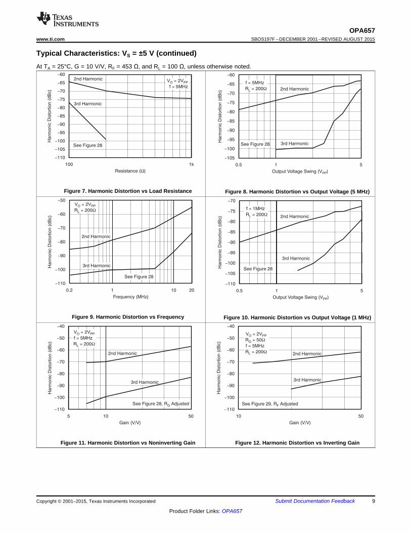
Typical Characteristics: VS = ±5 V (continued)At TA = 25°C, G = 10 V/V, RF = 453 Ω, and RL = 100 Ω, unless otherwise noted.
Figure 7. Harmonic Distortion vs Load Resistance Figure 8. Harmonic Distortion vs Output Voltage (5 MHz)
Figure 9. Harmonic Distortion vs Frequency Figure 10. Harmonic Distortion vs Output Voltage (1 MHz)
Figure 11. Harmonic Distortion vs Noninverting Gain Figure 12. Harmonic Distortion vs Inverting Gain
Copyright © 2001–2015, Texas Instruments Incorporated Submit Documentation Feedback 9
Product Folder Links: OPA657
10 100 1k
Capacitive Load (pF)
R(
SW
)
100
10
1
For Maximally-Flat Frequency Response
1 10 100 500
Frequency (MHz)
No
rma
lize
d G
ain
to
Ca
pa
citiv
e L
oa
d (
dB
) 23
20
17
14
11
8
5
2
RS
50W
1kW
VI
VO
CL
50W
453W
OPA657
C = 22pFL
C = 100pFL
C = 10pFL
1k 100k 1M 10M10k 100M
Frequency (Hz)
CM
RR
, P
SR
R (
dB
)
110
100
90
80
70
60
50
40
30
20
CMRR
+PSRR
-PSRR
–270
–225
–180
–135
–90
–45
0
45
–40
–20
0
20
40
60
80
100
Ope
nLo
op
Ga
in-
Ph
ase
() °
Ope
nLo
op
Ga
in-
Mag
nitu
de
(dB
)
Frequency (Hz)
Aol Magnitude
Aol Phase
D001
20log10(AOL)
ÐAOL
100 1k 10k 100k 1M 10M 100M 1G
-10 -8 -6 -4 -2 420 6 8
Single- ower (dBm)Tone Load P
3rd
-Ord
er
Sp
urio
us L
eve
l (d
Bc)
-50
-60
-70
-80
-90
-100
5MHz
15MHz
20MHz
10MHz
50W
50W
50W
PI
PO
50W
453W
OPA657
10 100 1k 10k 100k 1M 10M
Frequency (Hz)
e(n
V/
nÖ
), i
(fA
/n
Ö)
Hz
Hz
100
10
1
Input Voltage Noise 4.8nV/ÖHz
Input Current Noise 1.3fA/ÖHz
OPA657SBOS197F –DECEMBER 2001–REVISED AUGUST 2015 www.ti.com
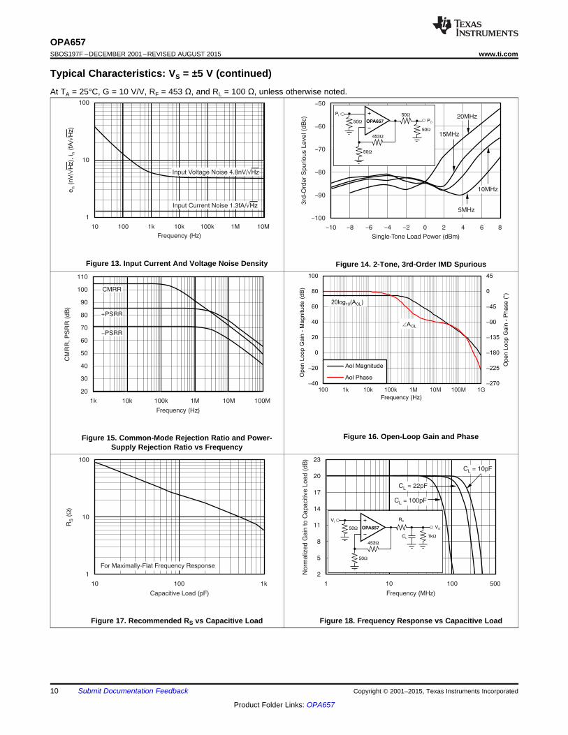
Typical Characteristics: VS = ±5 V (continued)At TA = 25°C, G = 10 V/V, RF = 453 Ω, and RL = 100 Ω, unless otherwise noted.
Figure 13. Input Current And Voltage Noise Density Figure 14. 2-Tone, 3rd-Order IMD Spurious
Figure 16. Open-Loop Gain and PhaseFigure 15. Common-Mode Rejection Ratio and Power-Supply Rejection Ratio vs Frequency
Figure 17. Recommended RS vs Capacitive Load Figure 18. Frequency Response vs Capacitive Load
10 Submit Documentation Feedback Copyright © 2001–2015, Texas Instruments Incorporated
Product Folder Links: OPA657
Time (20ns/div)
5
4
3
2
1
0
-1
-2
-3
-4
-5See Figure 29
Outp
ut V
oltage (
V) In
put V
olta
ge (V
)
0.25
0.2
0.15
0.1
0.05
0
-0.05
-0.1
-0.15
-0.2
-0.25
G = 20-
Output Voltage
Left Scale
Input Voltage
Right Scale
Time (20ns/div)
Ou
tpu
t V
olta
ge
(V
) Inpu
t Vo
ltag
e (V
)
5
4
3
2
1
0
-1
-2
-3
-4
-5
0.5
0.4
0.3
0.2
0.1
0
-0.1
-0.2
-0.3
-0.4
-0.5
G = +10
See Figure 28
Output Voltage
Left Scale
Input Voltage
Right Scale
-50 -25 0 25 50 75 100 125
Ambient Temperature ( C)°
Inp
ut
Bia
s C
urr
en
t (p
A)
1000
900
800
700
600
500
400
300
200
100
0
-50 -25 0 25 50 75 100 125
Ambient Temperature (°C)
Ou
tpu
t C
urr
en
t (2
5m
A/d
iv) S
up
ply
Cu
rren
t (3m
A/d
iv)
150
125
100
75
50
25
0
18
15
12
9
6
3
0
Supply Current Right Scale
Left Scale
Sourcing Current
Sinking Current
Left Scale
-50 -25 0 25 50 75 100 125
Ambient Temperature ( C)°
Inp
ut
Off
se
t V
olta
ge
(m
V)
1
0.5
0
-0.5
-1
-3 -2 -1 0 1 2 3
Common-Mode Input Voltage (V)
Inp
ut
Bia
s C
urr
en
t (p
A)
2
1.5
1
0.5
0
-0.5
-1
-1.5
-2
OPA657www.ti.com SBOS197F –DECEMBER 2001–REVISED AUGUST 2015
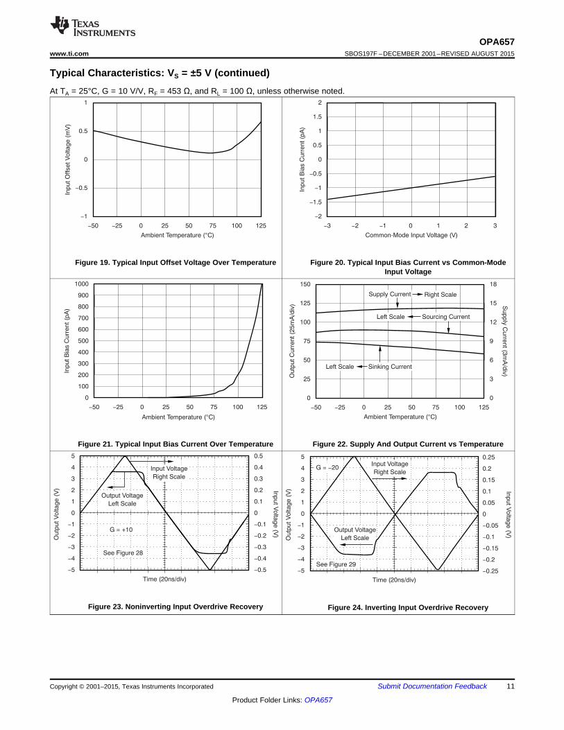
Typical Characteristics: VS = ±5 V (continued)At TA = 25°C, G = 10 V/V, RF = 453 Ω, and RL = 100 Ω, unless otherwise noted.
Figure 19. Typical Input Offset Voltage Over Temperature Figure 20. Typical Input Bias Current vs Common-ModeInput Voltage
Figure 21. Typical Input Bias Current Over Temperature Figure 22. Supply And Output Current vs Temperature
Figure 23. Noninverting Input Overdrive Recovery Figure 24. Inverting Input Overdrive Recovery
Copyright © 2001–2015, Texas Instruments Incorporated Submit Documentation Feedback 11
Product Folder Links: OPA657
-5 -4 -3 -2 -1 543210
Common-Mode Input Voltage (V)
CM
RR
(d
B)
110
90
70
50
-100 -80 -60 -40 -20 0 20 40 60 80 100
I (mA)O
V(V
)O
5
4
3
2
1
0
-1
-2
-3
-4
-5
1W Internal Power
R = 100WL
R = 50WL
R = 25WL
1W Internal Power
0.1 1 10 100
Frequency (MHz)
Outp
ut Im
pedance (
W)
10
1
0.1
0.01
ZO
50 Ω
453 Ω
OPA657
OPA657SBOS197F –DECEMBER 2001–REVISED AUGUST 2015 www.ti.com
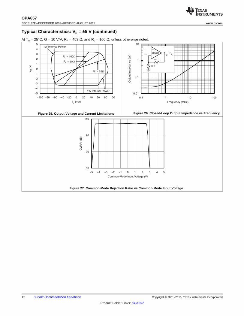
Typical Characteristics: VS = ±5 V (continued)At TA = 25°C, G = 10 V/V, RF = 453 Ω, and RL = 100 Ω, unless otherwise noted.
Figure 26. Closed-Loop Output Impedance vs FrequencyFigure 25. Output Voltage and Current Limitations
Figure 27. Common-Mode Rejection Ratio vs Common-Mode Input Voltage
12 Submit Documentation Feedback Copyright © 2001–2015, Texas Instruments Incorporated
Product Folder Links: OPA657
ExternalPin
+VCC
-VCC
InternalCircuitry
OPA657www.ti.com SBOS197F –DECEMBER 2001–REVISED AUGUST 2015
8 Detailed Description
8.1 OverviewThe OPA657 is high gain-bandwidth, voltage feedback operational amplifier featuring a low noise JFET inputstage. The OPA657 has been decompensated to allow for optimized Bandwidth to Quiescent currentperformance and better optimize its voltage noise performance. The OPA657 finds wide use in optical front-endapplications and in test and measurement systems that require high input impedance. It is built using a very highspeed complementary bipolar process.
8.2 Feature Description
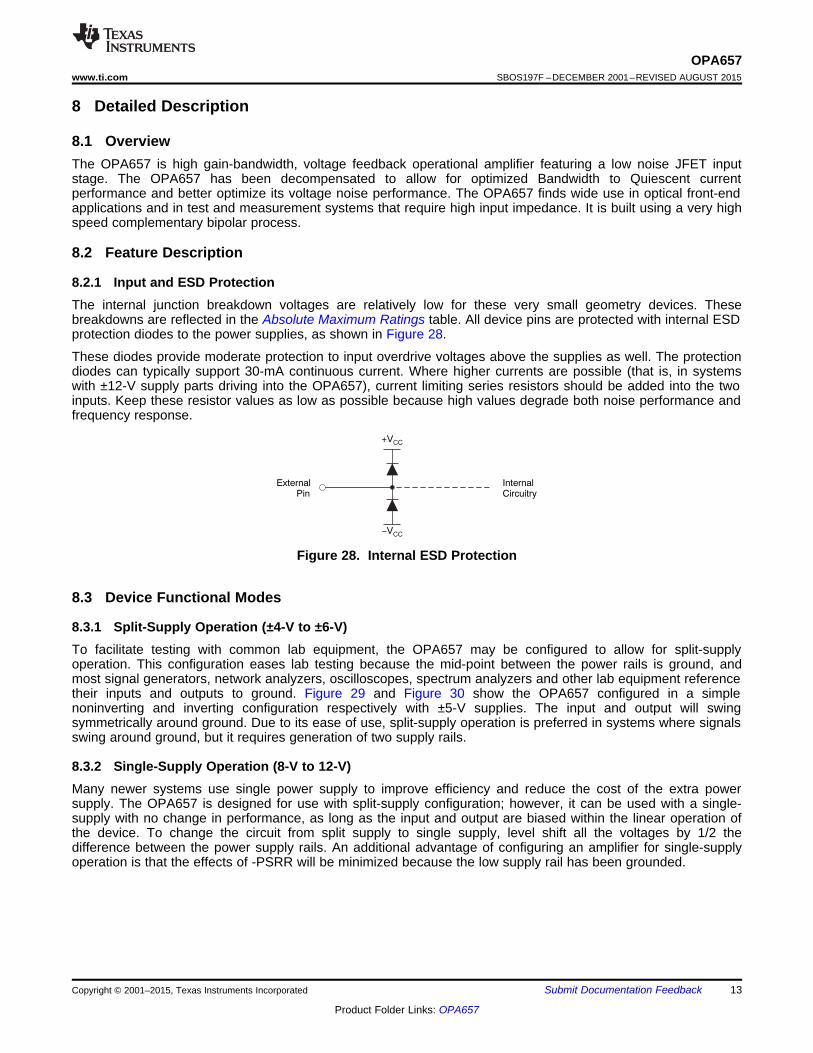
8.2.1 Input and ESD ProtectionThe internal junction breakdown voltages are relatively low for these very small geometry devices. Thesebreakdowns are reflected in the Absolute Maximum Ratings table. All device pins are protected with internal ESDprotection diodes to the power supplies, as shown in Figure 28.
These diodes provide moderate protection to input overdrive voltages above the supplies as well. The protectiondiodes can typically support 30-mA continuous current. Where higher currents are possible (that is, in systemswith ±12-V supply parts driving into the OPA657), current limiting series resistors should be added into the twoinputs. Keep these resistor values as low as possible because high values degrade both noise performance andfrequency response.
Figure 28. Internal ESD Protection
8.3 Device Functional Modes
8.3.1 Split-Supply Operation (±4-V to ±6-V)To facilitate testing with common lab equipment, the OPA657 may be configured to allow for split-supplyoperation. This configuration eases lab testing because the mid-point between the power rails is ground, andmost signal generators, network analyzers, oscilloscopes, spectrum analyzers and other lab equipment referencetheir inputs and outputs to ground. Figure 29 and Figure 30 show the OPA657 configured in a simplenoninverting and inverting configuration respectively with ±5-V supplies. The input and output will swingsymmetrically around ground. Due to its ease of use, split-supply operation is preferred in systems where signalsswing around ground, but it requires generation of two supply rails.
8.3.2 Single-Supply Operation (8-V to 12-V)Many newer systems use single power supply to improve efficiency and reduce the cost of the extra powersupply. The OPA657 is designed for use with split-supply configuration; however, it can be used with a single-supply with no change in performance, as long as the input and output are biased within the linear operation ofthe device. To change the circuit from split supply to single supply, level shift all the voltages by 1/2 thedifference between the power supply rails. An additional advantage of configuring an amplifier for single-supplyoperation is that the effects of -PSRR will be minimized because the low supply rail has been grounded.
Copyright © 2001–2015, Texas Instruments Incorporated Submit Documentation Feedback 13
Product Folder Links: OPA657
OPA657
+5V
-5V
-VS
+VS
50WVO
VI
50W
+0.1 Fm
+6.8 Fm
6.8 Fm
RG
50W
RF
453W
50 SourceW
50 LoadW
0.1 Fm
OPA657SBOS197F –DECEMBER 2001–REVISED AUGUST 2015 www.ti.com
9 Application and Implementation
NOTEInformation in the following applications sections is not part of the TI componentspecification, and TI does not warrant its accuracy or completeness. TI’s customers areresponsible for determining suitability of components for their purposes. Customers shouldvalidate and test their design implementation to confirm system functionality.
9.1 Application Information
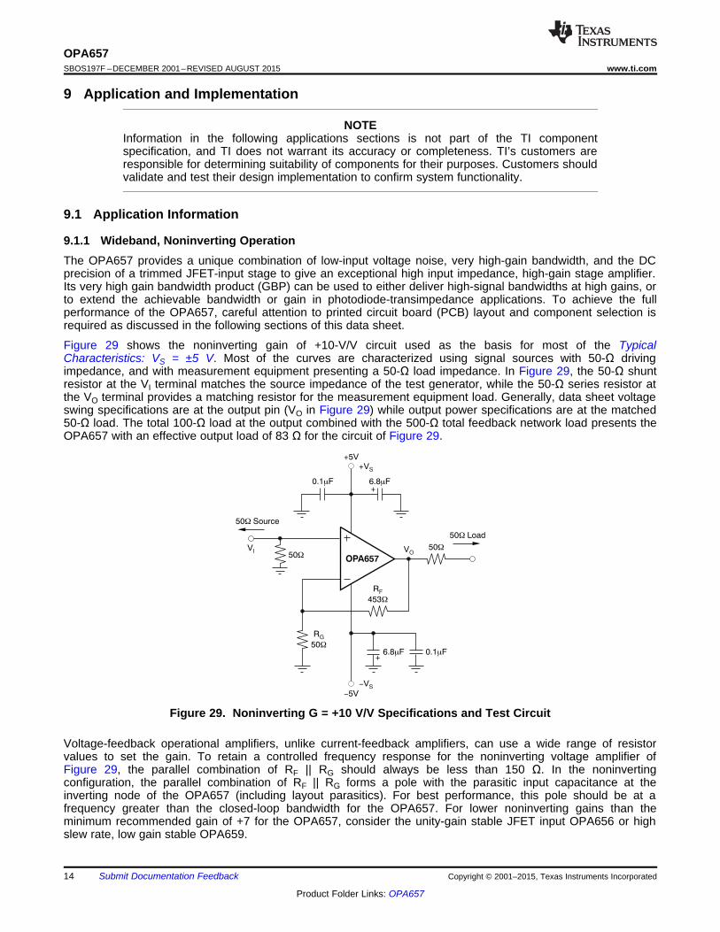
9.1.1 Wideband, Noninverting OperationThe OPA657 provides a unique combination of low-input voltage noise, very high-gain bandwidth, and the DCprecision of a trimmed JFET-input stage to give an exceptional high input impedance, high-gain stage amplifier.Its very high gain bandwidth product (GBP) can be used to either deliver high-signal bandwidths at high gains, orto extend the achievable bandwidth or gain in photodiode-transimpedance applications. To achieve the fullperformance of the OPA657, careful attention to printed circuit board (PCB) layout and component selection isrequired as discussed in the following sections of this data sheet.
Figure 29 shows the noninverting gain of +10-V/V circuit used as the basis for most of the TypicalCharacteristics: VS = ±5 V. Most of the curves are characterized using signal sources with 50-Ω drivingimpedance, and with measurement equipment presenting a 50-Ω load impedance. In Figure 29, the 50-Ω shuntresistor at the VI terminal matches the source impedance of the test generator, while the 50-Ω series resistor atthe VO terminal provides a matching resistor for the measurement equipment load. Generally, data sheet voltageswing specifications are at the output pin (VO in Figure 29) while output power specifications are at the matched50-Ω load. The total 100-Ω load at the output combined with the 500-Ω total feedback network load presents theOPA657 with an effective output load of 83 Ω for the circuit of Figure 29.
Figure 29. Noninverting G = +10 V/V Specifications and Test Circuit
Voltage-feedback operational amplifiers, unlike current-feedback amplifiers, can use a wide range of resistorvalues to set the gain. To retain a controlled frequency response for the noninverting voltage amplifier ofFigure 29, the parallel combination of RF || RG should always be less than 150 Ω. In the noninvertingconfiguration, the parallel combination of RF || RG forms a pole with the parasitic input capacitance at theinverting node of the OPA657 (including layout parasitics). For best performance, this pole should be at afrequency greater than the closed-loop bandwidth for the OPA657. For lower noninverting gains than theminimum recommended gain of +7 for the OPA657, consider the unity-gain stable JFET input OPA656 or highslew rate, low gain stable OPA659.
14 Submit Documentation Feedback Copyright © 2001–2015, Texas Instruments Incorporated
Product Folder Links: OPA657
OPA657
+5V
-5V
+VS
-VS
50WVO
VI
+6.8 Fm0.1 Fm
+6.8 Fm0.1 Fm
RF
1kW
RG
50W
50 SourceW
50 LoadW
OPA657www.ti.com SBOS197F –DECEMBER 2001–REVISED AUGUST 2015
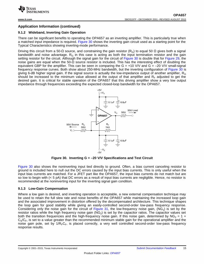
Application Information (continued)9.1.2 Wideband, Inverting Gain OperationThere can be significant benefits to operating the OPA657 as an inverting amplifier. This is particularly true whena matched input impedance is required. Figure 30 shows the inverting gain circuit used as a starting point for theTypical Characteristics showing inverting-mode performance.
Driving this circuit from a 50-Ω source, and constraining the gain resistor (RG) to equal 50 Ω gives both a signalbandwidth and noise advantage. RG in this case is acting as both the input termination resistor and the gainsetting resistor for the circuit. Although the signal gain for the circuit of Figure 30 is double that for Figure 29, thenoise gains are equal when the 50-Ω source resistor is included. This has the interesting effect of doubling theequivalent GBP for the amplifier. This can be seen in comparing the G = +10 V/V and G = –20 V/V small-signalfrequency response curves. Both show about 250-MHz bandwidth, but the inverting configuration of Figure 30 isgiving 6-dB higher signal gain. If the signal source is actually the low-impedance output of another amplifier, RGshould be increased to the minimum value allowed at the output of that amplifier and RF adjusted to get thedesired gain. It is critical for stable operation of the OPA657 that this driving amplifier show a very low outputimpedance through frequencies exceeding the expected closed-loop bandwidth for the OPA657.
Figure 30. Inverting G = –20 V/V Specifications and Test Circuit
Figure 30 also shows the noninverting input tied directly to ground. Often, a bias current canceling resistor toground is included here to null out the DC errors caused by the input bias currents. This is only useful when theinput bias currents are matched. For a JFET part like the OPA657, the input bias currents do not match but areso low to begin with (< 5 pA) that DC errors as a result of input bias currents are negligible. Hence, no resistor isrecommended at the noninverting input for the inverting signal gain condition.
9.1.3 Low-Gain CompensationWhere a low gain is desired, and inverting operation is acceptable, a new external compensation technique maybe used to retain the full slew rate and noise benefits of the OPA657 while maintaining the increased loop gainand the associated improvement in distortion offered by the decompensated architecture. This technique shapesthe loop gain for good stability while giving an easily-controlled second-order low-pass frequency response.Considering only the noise gain for the circuit of Figure 31, the low-frequency noise gain, (NG1) is set by theresistor ratios while the high frequency noise gain (NG2) is set by the capacitor ratios. The capacitor values setboth the transition frequencies and the high-frequency noise gain. If this noise gain, determined by NG2 = 1 +CS/CF, is set to a value greater than the recommended minimum stable gain for the operational amplifier and thenoise gain pole, set by 1/RFCF, is placed correctly, a very well controlled second-order low-pass frequencyresponse results.
Copyright © 2001–2015, Texas Instruments Incorporated Submit Documentation Feedback 15
Product Folder Links: OPA657
Z GBPO (= 130MHz)f @-3dB
C = (NG 1)C-S 2 F (= 27.2pF)
C =F
1
2 R Z NGp ´ F O 2
(= 2.86pF)
Z =O 1 2-
GBP
NG1
2
NG1
NG2
1 -
NG1
NG2
-
RF
500W
CS
27pF
OPA657
+5V
-5V
V = 2- ´ VO I
VI
CF
2.9pF
RG
250W
OPA657SBOS197F –DECEMBER 2001–REVISED AUGUST 2015 www.ti.com
Application Information (continued)
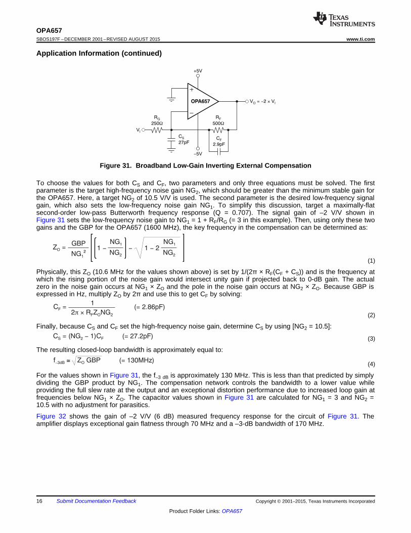
Figure 31. Broadband Low-Gain Inverting External Compensation
To choose the values for both CS and CF, two parameters and only three equations must be solved. The firstparameter is the target high-frequency noise gain NG2, which should be greater than the minimum stable gain forthe OPA657. Here, a target NG2 of 10.5 V/V is used. The second parameter is the desired low-frequency signalgain, which also sets the low-frequency noise gain NG1. To simplify this discussion, target a maximally-flatsecond-order low-pass Butterworth frequency response (Q = 0.707). The signal gain of –2 V/V shown inFigure 31 sets the low-frequency noise gain to NG1 = 1 + RF/RG (= 3 in this example). Then, using only these twogains and the GBP for the OPA657 (1600 MHz), the key frequency in the compensation can be determined as:
(1)
Physically, this ZO (10.6 MHz for the values shown above) is set by 1/(2π × RF(CF + CS)) and is the frequency atwhich the rising portion of the noise gain would intersect unity gain if projected back to 0-dB gain. The actualzero in the noise gain occurs at NG1 × ZO and the pole in the noise gain occurs at NG2 × ZO. Because GBP isexpressed in Hz, multiply ZO by 2π and use this to get CF by solving:
(2)
Finally, because CS and CF set the high-frequency noise gain, determine CS by using [NG2 = 10.5]:
(3)
The resulting closed-loop bandwidth is approximately equal to:
(4)
For the values shown in Figure 31, the f–3 dB is approximately 130 MHz. This is less than that predicted by simplydividing the GBP product by NG1. The compensation network controls the bandwidth to a lower value whileproviding the full slew rate at the output and an exceptional distortion performance due to increased loop gain atfrequencies below NG1 × ZO. The capacitor values shown in Figure 31 are calculated for NG1 = 3 and NG2 =10.5 with no adjustment for parasitics.
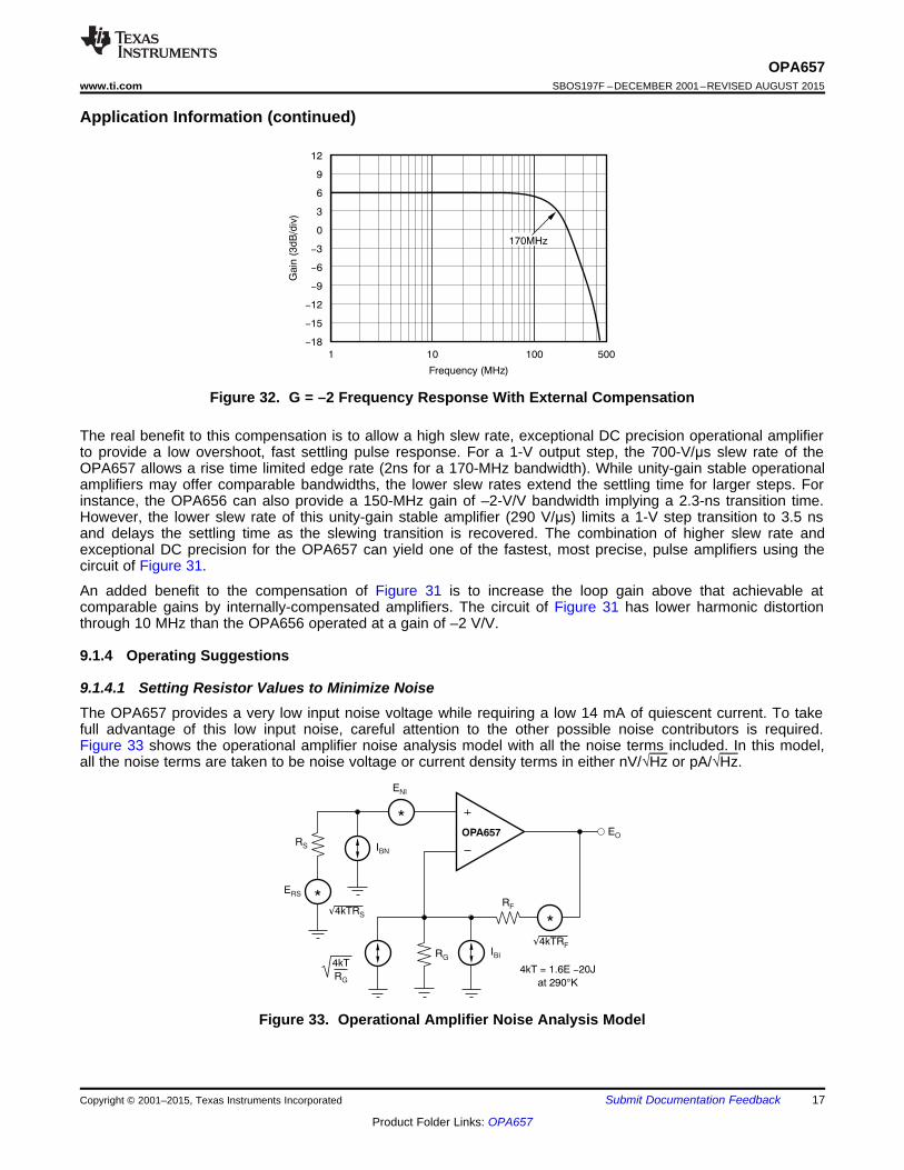
Figure 32 shows the gain of –2 V/V (6 dB) measured frequency response for the circuit of Figure 31. Theamplifier displays exceptional gain flatness through 70 MHz and a –3-dB bandwidth of 170 MHz.
16 Submit Documentation Feedback Copyright © 2001–2015, Texas Instruments Incorporated
Product Folder Links: OPA657
4kT
RG
RG
RF
RS
OPA657
IBI
EO
IBN
4kT = 1.6E 20J-
at 290 K°
ERS
ENI
Ö4kTRS
Ö4kTRF
*
*
*
12
9
6
3
0
-3
-6
-9
-12
-15
-18
Frequency (MHz)
Gain
(3dB
/div
)
1 10 100 500
170MHz
OPA657www.ti.com SBOS197F –DECEMBER 2001–REVISED AUGUST 2015
Application Information (continued)
Figure 32. G = –2 Frequency Response With External Compensation
The real benefit to this compensation is to allow a high slew rate, exceptional DC precision operational amplifierto provide a low overshoot, fast settling pulse response. For a 1-V output step, the 700-V/μs slew rate of theOPA657 allows a rise time limited edge rate (2ns for a 170-MHz bandwidth). While unity-gain stable operationalamplifiers may offer comparable bandwidths, the lower slew rates extend the settling time for larger steps. Forinstance, the OPA656 can also provide a 150-MHz gain of –2-V/V bandwidth implying a 2.3-ns transition time.However, the lower slew rate of this unity-gain stable amplifier (290 V/μs) limits a 1-V step transition to 3.5 nsand delays the settling time as the slewing transition is recovered. The combination of higher slew rate andexceptional DC precision for the OPA657 can yield one of the fastest, most precise, pulse amplifiers using thecircuit of Figure 31.
An added benefit to the compensation of Figure 31 is to increase the loop gain above that achievable atcomparable gains by internally-compensated amplifiers. The circuit of Figure 31 has lower harmonic distortionthrough 10 MHz than the OPA656 operated at a gain of –2 V/V.
9.1.4 Operating Suggestions
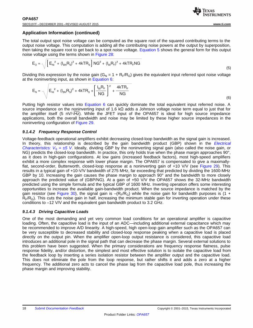
9.1.4.1 Setting Resistor Values to Minimize NoiseThe OPA657 provides a very low input noise voltage while requiring a low 14 mA of quiescent current. To takefull advantage of this low input noise, careful attention to the other possible noise contributors is required.Figure 33 shows the operational amplifier noise analysis model with all the noise terms included. In this model,all the noise terms are taken to be noise voltage or current density terms in either nV/√Hz or pA/√Hz.
Figure 33. Operational Amplifier Noise Analysis Model
Copyright © 2001–2015, Texas Instruments Incorporated Submit Documentation Feedback 17
Product Folder Links: OPA657
E + (I R ) + 4kTRNI BN S S +2 2E =N +
I RBI F
NG
2 4kTRF
NG
E + (I R ) + 4kTRNI BN S S
2 2E =O NG + (I R ) + 4kTR NGBI F F
2 2
OPA657SBOS197F –DECEMBER 2001–REVISED AUGUST 2015 www.ti.com
Application Information (continued)The total output spot noise voltage can be computed as the square root of the squared contributing terms to theoutput noise voltage. This computation is adding all the contributing noise powers at the output by superposition,then taking the square root to get back to a spot noise voltage. Equation 5 shows the general form for this outputnoise voltage using the terms shown in Figure 28:
(5)
Dividing this expression by the noise gain (GN = 1 + RF/RG) gives the equivalent input referred spot noise voltageat the noninverting input, as shown in Equation 6:
(6)
Putting high resistor values into Equation 6 can quickly dominate the total equivalent input referred noise. Asource impedance on the noninverting input of 1.6 kΩ adds a Johnson voltage noise term equal to just that forthe amplifier itself (5 nV/√Hz). While the JFET input of the OPA657 is ideal for high source impedanceapplications, both the overall bandwidth and noise may be limited by these higher source impedances in thenoninverting configuration of Figure 29.
9.1.4.2 Frequency Response ControlVoltage-feedback operational amplifiers exhibit decreasing closed-loop bandwidth as the signal gain is increased.In theory, this relationship is described by the gain bandwidth product (GBP) shown in the ElectricalCharacteristics: VS = ±5 V. Ideally, dividing GBP by the noninverting signal gain (also called the noise gain, orNG) predicts the closed-loop bandwidth. In practice, this only holds true when the phase margin approaches 90°,as it does in high-gain configurations. At low gains (increased feedback factors), most high-speed amplifiersexhibit a more complex response with lower phase margin. The OPA657 is compensated to give a maximally-flat, second-order, Butterworth, closed-loop response at a noninverting gain of +10 V/V (see Figure 29). Thisresults in a typical gain of +10-V/V bandwidth of 275 MHz, far exceeding that predicted by dividing the 1600-MHzGBP by 10. Increasing the gain causes the phase margin to approach 90° and the bandwidth to more closelyapproach the predicted value of (GBP/NG). At a gain of +50 V/V the OPA657 shows the 32-MHz bandwidthpredicted using the simple formula and the typical GBP of 1600 MHz. Inverting operation offers some interestingopportunities to increase the available gain-bandwidth product. When the source impedance is matched by thegain resistor (see Figure 30), the signal gain is –(RF/RG) while the noise gain for bandwidth purposes is (1 +RF/RG). This cuts the noise gain in half, increasing the minimum stable gain for inverting operation under theseconditions to –12 V/V and the equivalent gain bandwidth product to 3.2 GHz.
9.1.4.3 Driving Capacitive LoadsOne of the most demanding and yet very common load conditions for an operational amplifier is capacitiveloading. Often, the capacitive load is the input of an ADC—including additional external capacitance which maybe recommended to improve A/D linearity. A high-speed, high open-loop gain amplifier such as the OPA657 canbe very susceptible to decreased stability and closed-loop response peaking when a capacitive load is placeddirectly on the output pin. When the amplifier open-loop output resistance is considered, this capacitive loadintroduces an additional pole in the signal path that can decrease the phase margin. Several external solutions tothis problem have been suggested. When the primary considerations are frequency response flatness, pulseresponse fidelity, and/or distortion, the simplest and most effective solution is to isolate the capacitive load fromthe feedback loop by inserting a series isolation resistor between the amplifier output and the capacitive load.This does not eliminate the pole from the loop response, but rather shifts it and adds a zero at a higherfrequency. The additional zero acts to cancel the phase lag from the capacitive load pole, thus increasing thephase margin and improving stability.
18 Submit Documentation Feedback Copyright © 2001–2015, Texas Instruments Incorporated
Product Folder Links: OPA657
OPA657www.ti.com SBOS197F –DECEMBER 2001–REVISED AUGUST 2015
Application Information (continued)The Typical Characteristics illustrate the Recommended RS vs Capacitive Load (Figure 17) and the resultingfrequency response at the load. In this case, a design target of a maximally-flat frequency response is used.Lower values of RS may be used if some peaking can be tolerated. Also, operating at higher gains (than the +10V/V used in the Typical Characteristics) require lower values of RS for a minimally-peaked frequency response.Parasitic capacitive loads greater than 2 pF can begin to degrade the performance of the OPA657. Long PCboard traces, unmatched cables, and connections to multiple devices can easily cause this value to beexceeded. Always consider this effect carefully, and add the recommended series resistor as close as possible tothe OPA657 output pin (see the Layout Guidelines section).
9.1.4.4 Distortion PerformanceThe OPA657 is capable of delivering a low-distortion signal at high frequencies over a wide range of gains. Thedistortion plots in the Typical Characteristics: VS = ±5 V show the typical distortion under a wide variety ofconditions.
Generally, until the fundamental signal reaches very high frequencies or powers, the second-harmonic dominatesthe distortion with a negligible third-harmonic component. Focusing then on the second-harmonic, increasing theload impedance improves distortion directly. Remember that the total load includes the feedback network—in thenoninverting configuration this is sum of RF + RG, while in the inverting configuration this is just RF (seeFigure 29). Increasing output voltage swing increases harmonic distortion directly. A 6-dB increase in outputswing generally increases the second-harmonic 12 dB and the third-harmonic 18 dB. Increasing the signal gainalso increases the second-harmonic distortion. Again, a 6-dB increase in gain increases the second- and third-harmonic by approximately 6 dB, even with a constant output power and frequency. And finally, the distortionincreases as the fundamental frequency increases due to the roll-off in the loop gain with frequency. Conversely,the distortion improves going to lower frequencies down to the dominant open-loop pole at approximately 100kHz. Starting from the –70-dBc second-harmonic for a 5-MHz, 2 VPP fundamental into a 200-Ω load at G = +10V/V (from the Typical Characteristics: VS = ±5 V), the second-harmonic distortion for frequencies lower than 100kHz is approximately less than –90 dBc.
The OPA657 has an extremely low third-order harmonic distortion. This also shows up in the two-tone, third-order, intermodulation spurious (IM3) response curves. The third-order spurious levels are extremely low (< –80dBc) at low output power levels. The output stage continues to hold them low even as the fundamental powerreaches higher levels. As shown in Typical Characteristics: VS = ±5 V, the spurious intermodulation powers donot increase as predicted by a traditional intercept model. As the fundamental power level increases, thedynamic range does not decrease significantly. For two tones centered at 10 MHz, with 4 dBm/tone into amatched 50-Ω load (that is, 1 VPP for each tone at the load, which requires 4 VPP for the overall two-toneenvelope at the output pin), the Typical Characteristics: VS = ±5 V show a 82-dBc difference between the testtone and the third-order intermodulation spurious levels. This exceptional performance improves further whenoperating at lower frequencies and/or higher load impedances.
9.1.4.5 DC Accuracy and Offset ControlThe OPA657 can provide excellent DC accuracy due to its high open-loop gain, high common-mode rejection,high power-supply rejection, and its trimmed input offset voltage (and drift) along with the negligible errorsintroduced by the low input bias current. For the best DC precision, a high-grade version (OPA657UB orOPA657NB) screens the key DC parameters to an even tighter limit. Both standard- and high-grade versionstake advantage of a new final test technique to 100% test input offset voltage drift over temperature. Thisdiscussion uses the high-grade typical and min/max Electrical Characteristics: VS = ±5 V for illustration; however,an identical analysis applies to the standard-grade version.
The total output DC offset voltage in any configuration and temperature is the combination of a number ofpossible error terms. In a JFET part such as the OPA657, the input bias current terms are typically quite low butare unmatched. Using bias-current cancellation techniques, more typical in bipolar input amplifiers, does notimprove output DC offset errors. Errors due to the input bias current only become dominant at elevatedtemperatures. The OPA657 shows the typical 2× increase in every 10°C common to JFET-input stage amplifiers.Using the 5-pA maximum tested value at +25°C, and a +20°C internal self heating (see thermal analysis), themaximum input bias current at +85°C ambient is 5 pA × 2(105 – 25)/10 = 1280 pA. For noninverting configurations,
Copyright © 2001–2015, Texas Instruments Incorporated Submit Documentation Feedback 19
Product Folder Links: OPA657
OPA657SBOS197F –DECEMBER 2001–REVISED AUGUST 2015 www.ti.com
Application Information (continued)this term only begins to be a significant term versus the input offset voltage for source impedances greater than750 kΩ. This would also be the feedback resistor value for transimpedance applications (see Figure 34) wherethe output DC error due to inverting input bias current is on the order of that contributed by the input offsetvoltage. In general, except for these extremely high-impedance values, the output DC errors due to the input biascurrent may be neglected.
After the input offset voltage itself, the most significant term contributing to output offset voltage is the PSRR forthe negative supply. This term is modeled as an input offset voltage shift due to changes in the negative power-supply voltage (and similarly for the +PSRR). The high-grade test limit for –PSRR is 68 dB. This translates into0.4-mV/V input offset voltage shift = 10(–68/20). This low sensitivity to the negative supply voltage requires a 1.5-Vchange in the negative supply to match the ±0.6mV input offset voltage error. The +PSRR is tested to aminimum value of 78 dB. This translates into 10(–78/20) = 0.125 mV/V sensitivity for the input offset voltage topositive power-supply changes.
As an example, compute the worst-case output DC error for the transimpedance circuit of Figure 34 at 25°C andthen the shift over the 0°C to 70°C range given the following assumptions.
Negative Power Supply= –5 V ±0.2 V with a ±5 mV/°C worst-case shift
Positive Power Supply= +5 V ±0.2 V with a ±5 mV/°C worst-case shift
Initial 25°C Output DC Error Band= ±0.6 mV (OPA657 high-grade input offset voltage limit)±0.08 mV (due to the –PSRR = 0.4 mV/V × ±0.2 V)±0.04 mV (due to the +PSRR = 0.2 mV/V × ±0.2 V)
Total = ±0.72mV
This would be the worst-case error band in volume production at 25°C acceptance testing given the conditionsstated. Over the temperature range (0°C to 70°C), expect the following worst-case shifting from initial value. A20°C internal junction self-heating is assumed here.
±0.36 mV (OPA657 high-grade input offset drift)= ±6 μV/°C × (70°C + 20°C – 25°C)
±0.11 mV (–PSRR of 66dB with 5mV × (70°C – 25°C) supply shift)
±0.04 mV (+PSRR of 76dB with 5mV × (70°C – 25°C) supply shift)
Total = ±0.51mV
This would be the worst-case shift from an initial offset over a 0°C to 70°C ambient for the conditions stated.Typical initial output DC error bands and shifts over temperature are much lower than these worst-caseestimates.
In the transimpedance configuration, the CMRR errors can be neglected because the input common-modevoltage is held at ground. For noninverting gain configurations (see Figure 29), the CMRR term needs to beconsidered but is typically far lower than the input offset voltage term. With a tested minimum of 91 dB (28 μV/V),the added apparent DC error is no more than ±0.06 mV for a ±2-V input swing to the circuit of Figure 29.
20 Submit Documentation Feedback Copyright © 2001–2015, Texas Instruments Incorporated
Product Folder Links: OPA657
1
2 R CpF F
=GBP
4 R CpF D
VB
+
CD
49 pF
CPCB
0.3 pF
OPA657
+5 V
-5 V
CF + CPCB
0.55 pF
RS
50 Oscilloscope
with 50 Inputs
RF
200 k
Supply Decoupling not shown
OPA657www.ti.com SBOS197F –DECEMBER 2001–REVISED AUGUST 2015
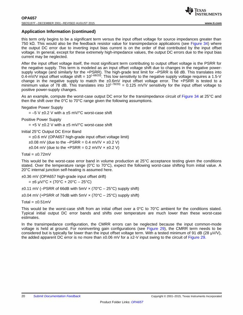
9.2 Typical ApplicationThe high GBP and low input voltage and current noise for the OPA657 make it an ideal widebandtransimpedance amplifier for moderate to high transimpedance gains. Unity-gain stability in the operationalamplifier is not required for application as a transimpedance amplifier.
Figure 34. Wideband, High-Sensitivity, Transimpedance Amplifier Diagram
9.2.1 Design RequirementsDesign a high-bandwidth, high-gain transimpedance amplifier with the design requirements shown in Table 1.
Table 1. Design RequirementsTARGET BANDWIDTH (MHz) TRANSIMPEDANCE GAIN (kΩ) PHOTODIODE CAPACITANCE (pF)
1 200 49
9.2.2 Detailed Design ProcedureDesigns that require high bandwidth from a large area detector with relatively high transimpedance gain benefitfrom the low input voltage noise of the OPA657. This input voltage noise is peaked up over frequency by thediode source capacitance, and can, in many cases, become the limiting factor to input sensitivity. The keyelements to the design are the expected diode capacitance (CD) with the reverse bias voltage (VB) applied, thedesired transimpedance gain, RF, and the GBP for the OPA657 (1600 MHz). Figure 34 shows a transimpedancecircuit with the parameters as described in Table 1. With these three variables set (and including the parasiticinput capacitance for the OPA657 and the PCB added to CD), the feedback capacitor value (CF) may be set tocontrol the frequency response. To achieve a maximally-flat second-order Butterworth frequency response, thefeedback pole should be set to:
(7)
Adding the common-mode and differential mode input capacitance (0.7 + 4.5) pF and the trace PCB capacitanceof approximately 0.3 pF to the 49-pF diode source capacitance of Figure 34, and targeting a 200-kΩtransimpedance gain using the 1600-MHz GBP for the OPA657 requires a feedback pole set to 3.5 MHz. Thisrequires a total feedback capacitance of 0.2 pF. Such low capacitance values are difficult to achieve due toparasitics from the PCB and the surface mount components.
Copyright © 2001–2015, Texas Instruments Incorporated Submit Documentation Feedback 21
Product Folder Links: OPA657
Frequency (Hz)
Outp
ut N
ois
e(n
V/v
Hz)
10
20
30
50
70
100
200
300
500
700
1000
D002
100 1k 10k 100k 1M 10M 100MFrequency (Hz)
Outp
ut N
ois
e(n
V/v
Hz)
10010
20
30
50
70
100
200
300
500
700
1000
D004
1k 10k 100k 1M 10M 100M
( )3dB F Df GBP / 2 R C Hz- = p
OPA657SBOS197F –DECEMBER 2001–REVISED AUGUST 2015 www.ti.com
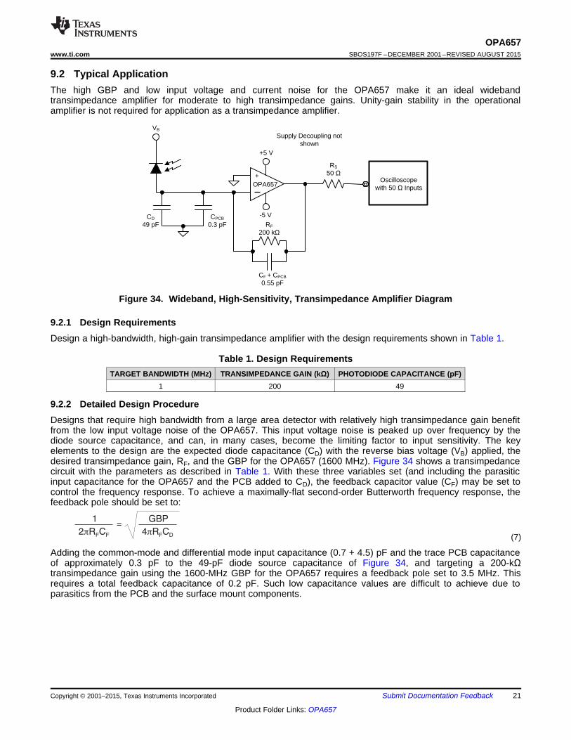
Equation 8 gives the approximate closed loop bandwidth of the system to be 4.8 MHz. Because the targetbandwidth is only 1 MHz, the feedback capacitance can be increased to a more practical value while maintainingthe bandwidth requirements of the design. A feedback capacitance of 0.550 pf was chosen. This includes thephysical 0.4-pF feedback capacitor in addition to the 0.1-pF parasitic capacitance from the feedback resistor andaround 50-fF capacitance from the PCB traces. Removing the ground and power planes from under the surfacemount components helps to minimize this parasitic capacitance. The simulated closed loop bandwidth ofFigure 34 was 1.7 MHz. The phase margin was close to 82°. This design should result in a system withnegligible overshoot to a pulsed input.
(8)
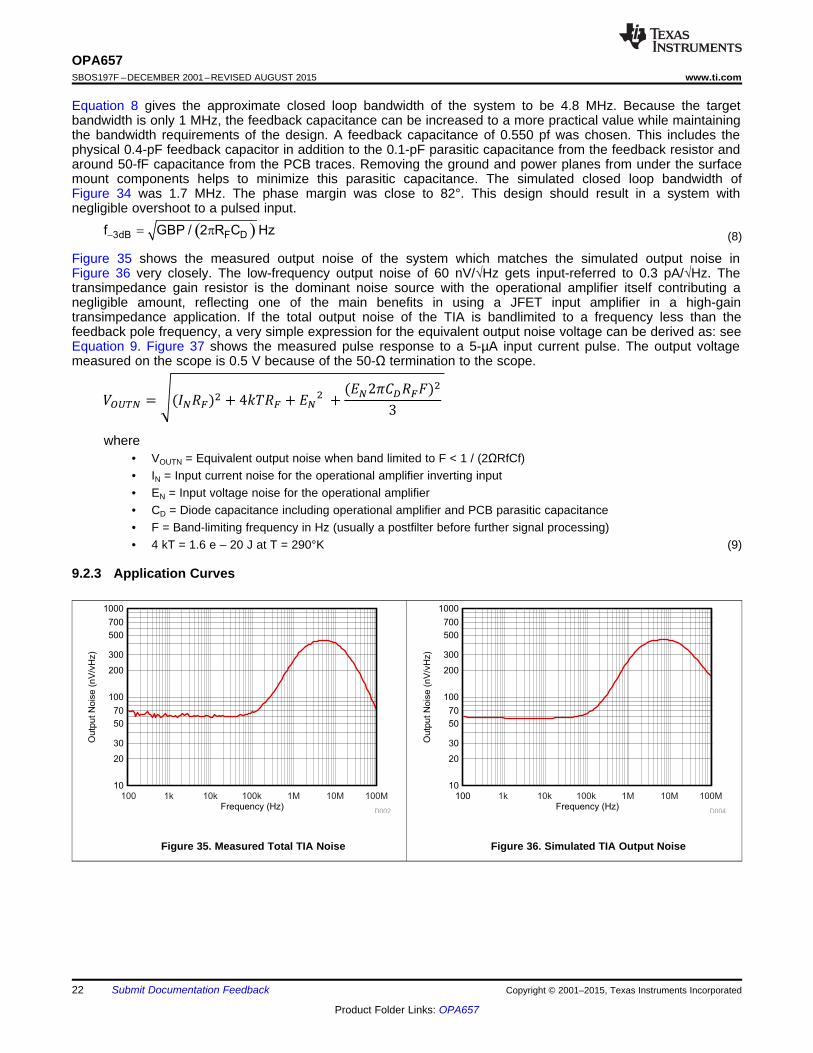
Figure 35 shows the measured output noise of the system which matches the simulated output noise inFigure 36 very closely. The low-frequency output noise of 60 nV/√Hz gets input-referred to 0.3 pA/√Hz. Thetransimpedance gain resistor is the dominant noise source with the operational amplifier itself contributing anegligible amount, reflecting one of the main benefits in using a JFET input amplifier in a high-gaintransimpedance application. If the total output noise of the TIA is bandlimited to a frequency less than thefeedback pole frequency, a very simple expression for the equivalent output noise voltage can be derived as: seeEquation 9. Figure 37 shows the measured pulse response to a 5-µA input current pulse. The output voltagemeasured on the scope is 0.5 V because of the 50-Ω termination to the scope.
where• VOUTN = Equivalent output noise when band limited to F < 1 / (2ΩRfCf)• IN = Input current noise for the operational amplifier inverting input• EN = Input voltage noise for the operational amplifier• CD = Diode capacitance including operational amplifier and PCB parasitic capacitance• F = Band-limiting frequency in Hz (usually a postfilter before further signal processing)• 4 kT = 1.6 e – 20 J at T = 290°K (9)
9.2.3 Application Curves
Figure 35. Measured Total TIA Noise Figure 36. Simulated TIA Output Noise
22 Submit Documentation Feedback Copyright © 2001–2015, Texas Instruments Incorporated
Product Folder Links: OPA657
Time (usec)
Out
put V
olta
ge (
V)
0 5 10 15 20 25 30 35 40 45-0.6
-0.5
-0.4
-0.3
-0.2
-0.1
0
0.1
D003
OPA657www.ti.com SBOS197F –DECEMBER 2001–REVISED AUGUST 2015
Rise Time = 239 ns Fall Time = 224 ns
Figure 37. Transient Pulse Response to 5-µA Input Current Pulse
Copyright © 2001–2015, Texas Instruments Incorporated Submit Documentation Feedback 23
Product Folder Links: OPA657
OPA657SBOS197F –DECEMBER 2001–REVISED AUGUST 2015 www.ti.com
10 Power Supply RecommendationsThe OPA657 is principally intended to work in a supply range of ±4 V to ±6 V. Good power-supply bypassing isrequired. Minimize the distance (<0.1 inch) from the power-supply pins to high frequency, 0.1-μF decouplingcapacitors. Often a larger capacitor (2.2 µF is typical) is used along with a high-frequency, 0.1-µF supplydecoupling capacitor at the device supply pins. For single-supply operation, only the positive supply has thesecapacitors. When a split supply is used, use these capacitors for each supply to ground. If necessary, place thelarger capacitors somewhat farther from the device and share these capacitors among several devices in thesame area of the PCB. Avoid narrow power and ground traces to minimize inductance between the pins and thedecoupling capacitors. An optional supply decoupling capacitor across the two power supplies (for bipolaroperation) improves second harmonic distortion performance.
11 Layout
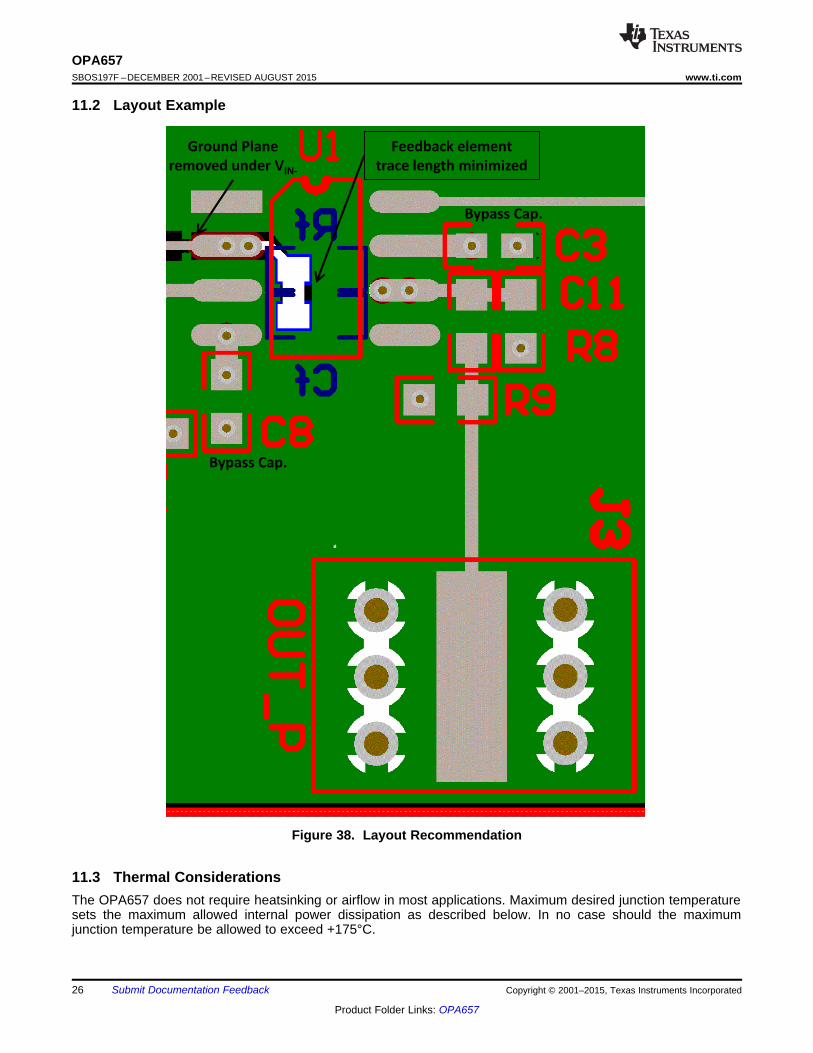
11.1 Layout GuidelinesAchieving optimum performance with a high-frequency amplifier such as the OPA657 requires careful attention toboard layout parasitics and external component types. Recommendations that optimize performance include:1. Minimize parasitic capacitance to any AC ground for all of the signal I/O pins. Parasitic capacitance on the
output and inverting input pins can cause instability—on the noninverting input, it can react with the sourceimpedance to cause unintentional bandlimiting. To reduce unwanted capacitance, a window around thesignal I/O pins should be opened in all of the ground and power planes around those pins. Otherwise, groundand power planes should be unbroken elsewhere on the board.
2. Minimize the distance (< 0.25") from the power-supply pins to high-frequency 0.1-μF decoupling capacitors.At the device pins, the ground and power-plane layout should not be in close proximity to the signal I/O pins.Avoid narrow power and ground traces to minimize inductance between the pins and the decouplingcapacitors. The power-supply connections should always be decoupled with these capacitors. Larger (2.2 μFto 6.8 μF) decoupling capacitors, effective at lower frequency, should also be used on the supply pins. Thesemay be placed somewhat farther from the device and may be shared among several devices in the samearea of the PC board.
3. Careful selection and placement of external components preserve the high-frequency performance ofthe OPA657. Resistors should be a very low reactance type. Surface-mount resistors work best and allow atighter overall layout. Metal film and carbon composition axially leaded resistors can also provide good high-frequency performance. Again, keep the leads and PCB trace length as short as possible. Never usewirewound-type resistors in a high-frequency application. Because the output pin and inverting input pin arethe most sensitive to parasitic capacitance, always position the feedback and series output resistor, if any, asclose as possible to the output pin. Other network components, such as noninverting input terminationresistors, should also be placed close to the package. Where double-side component mounting is allowed,place the feedback resistor directly under the package on the other side of the board between the output andinverting input pins. Even with a low parasitic capacitance shunting the external resistors, excessively highresistor values can create significant time constants that can degrade performance. Good axial metal film orsurface-mount resistors have approximately 0.2 pF in shunt with the resistor. For resistor values greater than1.5 kΩ, this parasitic capacitance can add a pole and/or zero below 500 MHz that can effect circuit operation.Keep resistor values as low as possible consistent with load driving considerations. It has been suggestedhere that a good starting point for design would be to keep RF || RG < 150 Ω for voltage amplifierapplications. Doing this automatically keeps the resistor noise terms low, and minimizes the effect of theparasitic capacitance. Transimpedance applications (see Figure 34) can use whatever feedback resistor isrequired by the application as long as the feedback-compensation capacitor is set considering all parasiticcapacitance terms on the inverting node.
4. Connections to other wideband devices on the board may be made with short direct traces or throughonboard transmission lines. For short connections, consider the trace and the input to the next device as alumped capacitive load. Relatively wide traces (50 mils to 100 mils) should be used, preferably with groundand power planes opened up around them. Estimate the total capacitive load and set RS from the plot ofRecommended RS vs Capacitive Load (Figure 17). Low parasitic capacitive loads (< 5 pF) may not need anRS because the OPA657 is nominally compensated to operate with a 2-pF parasitic load. Higher parasiticcapacitive loads without an RS are allowed as the signal gain increases (increasing the unloaded phasemargin). If a long trace is required, and the 6-dB signal loss intrinsic to a doubly-terminated transmission lineis acceptable, implement a matched-impedance transmission line using microstrip or stripline techniques
24 Submit Documentation Feedback Copyright © 2001–2015, Texas Instruments Incorporated
Product Folder Links: OPA657
OPA657www.ti.com SBOS197F –DECEMBER 2001–REVISED AUGUST 2015
Layout Guidelines (continued)(consult an ECL design handbook for microstrip and stripline layout techniques). A 50-Ω environment isnormally not necessary onboard, and in fact a higher impedance environment improves distortion, as shownin the distortion versus load plots. With a characteristic board trace impedance defined based on boardmaterial and trace dimensions, a matching series resistor into the trace from the output of the OPA657 isused as well as a terminating shunt resistor at the input of the destination device. Remember also that theterminating impedance is the parallel combination of the shunt resistor and the input impedance of thedestination device—this total effective impedance should be set to match the trace impedance. If the 6-dBattenuation of a doubly-terminated transmission line is unacceptable, a long trace can be series-terminatedat the source end only. Treat the trace as a capacitive load in this case and set the series resistor value asshown in the plot of RS vs Capacitive Load. This does not preserve signal integrity as well as a doubly-terminated line. If the input impedance of the destination device is low, there will be some signal attenuationdue to the voltage divider formed by the series output into the terminating impedance.
5. Socketing a high-speed part like the OPA657 is not recommended. The additional lead length and pin-to-pin capacitance introduced by the socket can create an extremely troublesome parasitic network whichcan make it almost impossible to achieve a smooth, stable frequency response. Best results are obtained bysoldering the OPA657 onto the board.
11.1.1 Demonstration FixturesTwo printed circuit boards (PCBs) are available to assist in the initial evaluation of circuit performance using theOPA657 in its two package options. Both of these are offered free of charge as unpopulated PCBs, deliveredwith a user's guide. The summary information for these fixtures is shown in Table 2.
Table 2. Demonstration Fixtures by PackagePRODUCT PACKAGE ORDERING NUMBER LITERATURE NUMBER
OPA657U SO-8 DEM-OPA-SO-1A SBOU009
OPA657N SOT23-5 DEM-OPA-SOT-1A SBOU010
The demonstration fixtures can be requested at the Texas Instruments website (www.ti.com) through theOPA657 product folder.
Copyright © 2001–2015, Texas Instruments Incorporated Submit Documentation Feedback 25
Product Folder Links: OPA657
Bypass Cap.
Bypass Cap.
Feedback element
trace length minimized
Ground Plane
removed under VIN-
OPA657SBOS197F –DECEMBER 2001–REVISED AUGUST 2015 www.ti.com
11.2 Layout Example
Figure 38. Layout Recommendation
11.3 Thermal ConsiderationsThe OPA657 does not require heatsinking or airflow in most applications. Maximum desired junction temperaturesets the maximum allowed internal power dissipation as described below. In no case should the maximumjunction temperature be allowed to exceed +175°C.
26 Submit Documentation Feedback Copyright © 2001–2015, Texas Instruments Incorporated
Product Folder Links: OPA657
Maximum T = +85 C + (0.25W 150 C/W) = 121 C° ´J ° °
P = 10V 16.1mA + 5 /(4 (100 ||500 )) = 236mW´ W WD ´2
OPA657www.ti.com SBOS197F –DECEMBER 2001–REVISED AUGUST 2015
Thermal Considerations (continued)Operating junction temperature (TJ) is given by TA + PD × θJA. The total internal power dissipation (PD) is the sumof quiescent power (PDQ) and additional power dissipated in the output stage (PDL) to deliver load power.Quiescent power is simply the specified no-load supply current times the total supply voltage across the part. PDLdepends on the required output signal and load but will—for a grounded resistive load—be at a maximum whenthe output is fixed at a voltage equal to 1/2 of either supply voltage (for equal bipolar supplies). Under thiscondition PDL = VS 2 / (4 × RL) where RL includes feedback network loading.
It is the power in the output stage and not into the load that determines internal power dissipation.
As a worst-case example, compute the maximum TJ using an OPA657N (SOT23-5 package) in the circuit ofFigure 29 operating at the maximum specified ambient temperature of +85°C and driving a grounded 100-Ω load.
(10)
(11)
All actual applications are operating at lower internal power and junction temperature.
Copyright © 2001–2015, Texas Instruments Incorporated Submit Documentation Feedback 27
Product Folder Links: OPA657
OPA657SBOS197F –DECEMBER 2001–REVISED AUGUST 2015 www.ti.com
12 Device and Documentation Support
12.1 Community ResourcesThe following links connect to TI community resources. Linked contents are provided "AS IS" by the respectivecontributors. They do not constitute TI specifications and do not necessarily reflect TI's views; see TI's Terms ofUse.
TI E2E™ Online Community TI's Engineer-to-Engineer (E2E) Community. Created to foster collaborationamong engineers. At e2e.ti.com, you can ask questions, share knowledge, explore ideas and helpsolve problems with fellow engineers.
Design Support TI's Design Support Quickly find helpful E2E forums along with design support tools andcontact information for technical support.
12.2 TrademarksE2E is a trademark of Texas Instruments.All other trademarks are the property of their respective owners.
12.3 Electrostatic Discharge CautionThese devices have limited built-in ESD protection. The leads should be shorted together or the device placed in conductive foamduring storage or handling to prevent electrostatic damage to the MOS gates.
12.4 GlossarySLYZ022 — TI Glossary.
This glossary lists and explains terms, acronyms, and definitions.
13 Mechanical, Packaging, and Orderable InformationThe following pages include mechanical, packaging, and orderable information. This information is the mostcurrent data available for the designated devices. This data is subject to change without notice and revision ofthis document. For browser-based versions of this data sheet, refer to the left-hand navigation.
28 Submit Documentation Feedback Copyright © 2001–2015, Texas Instruments Incorporated
Product Folder Links: OPA657
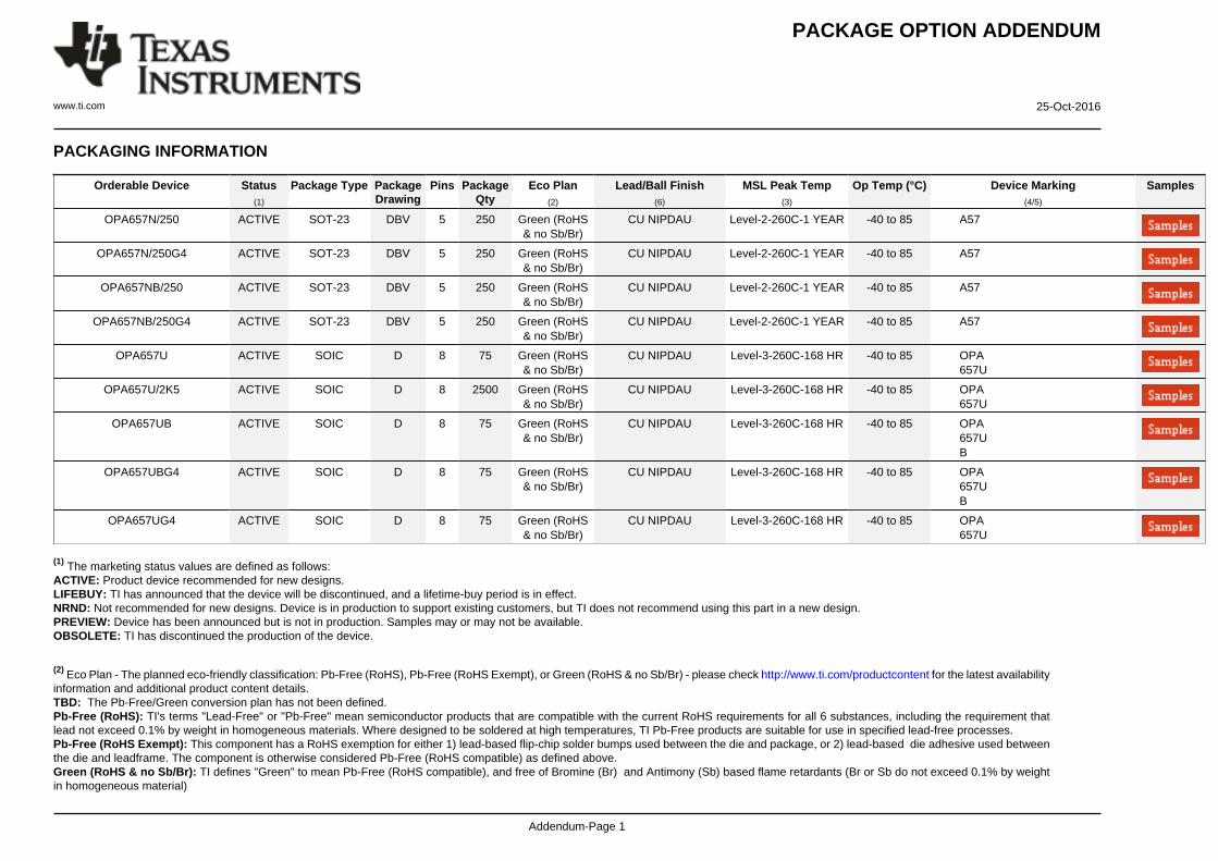
PACKAGE OPTION ADDENDUM
www.ti.com 25-Oct-2016
Addendum-Page 1
PACKAGING INFORMATION
Orderable Device Status(1)
Package Type PackageDrawing
Pins PackageQty
Eco Plan(2)
Lead/Ball Finish(6)
MSL Peak Temp(3)
Op Temp (°C) Device Marking(4/5)
Samples
OPA657N/250 ACTIVE SOT-23 DBV 5 250 Green (RoHS& no Sb/Br)
CU NIPDAU Level-2-260C-1 YEAR -40 to 85 A57
OPA657N/250G4 ACTIVE SOT-23 DBV 5 250 Green (RoHS& no Sb/Br)
CU NIPDAU Level-2-260C-1 YEAR -40 to 85 A57
OPA657NB/250 ACTIVE SOT-23 DBV 5 250 Green (RoHS& no Sb/Br)
CU NIPDAU Level-2-260C-1 YEAR -40 to 85 A57
OPA657NB/250G4 ACTIVE SOT-23 DBV 5 250 Green (RoHS& no Sb/Br)
CU NIPDAU Level-2-260C-1 YEAR -40 to 85 A57
OPA657U ACTIVE SOIC D 8 75 Green (RoHS& no Sb/Br)
CU NIPDAU Level-3-260C-168 HR -40 to 85 OPA657U
OPA657U/2K5 ACTIVE SOIC D 8 2500 Green (RoHS& no Sb/Br)
CU NIPDAU Level-3-260C-168 HR -40 to 85 OPA657U
OPA657UB ACTIVE SOIC D 8 75 Green (RoHS& no Sb/Br)
CU NIPDAU Level-3-260C-168 HR -40 to 85 OPA657UB
OPA657UBG4 ACTIVE SOIC D 8 75 Green (RoHS& no Sb/Br)
CU NIPDAU Level-3-260C-168 HR -40 to 85 OPA657UB
OPA657UG4 ACTIVE SOIC D 8 75 Green (RoHS& no Sb/Br)
CU NIPDAU Level-3-260C-168 HR -40 to 85 OPA657U
(1) The marketing status values are defined as follows:ACTIVE: Product device recommended for new designs.LIFEBUY: TI has announced that the device will be discontinued, and a lifetime-buy period is in effect.NRND: Not recommended for new designs. Device is in production to support existing customers, but TI does not recommend using this part in a new design.PREVIEW: Device has been announced but is not in production. Samples may or may not be available.OBSOLETE: TI has discontinued the production of the device.
(2) Eco Plan - The planned eco-friendly classification: Pb-Free (RoHS), Pb-Free (RoHS Exempt), or Green (RoHS & no Sb/Br) - please check http://www.ti.com/productcontent for the latest availabilityinformation and additional product content details.TBD: The Pb-Free/Green conversion plan has not been defined.Pb-Free (RoHS): TI's terms "Lead-Free" or "Pb-Free" mean semiconductor products that are compatible with the current RoHS requirements for all 6 substances, including the requirement thatlead not exceed 0.1% by weight in homogeneous materials. Where designed to be soldered at high temperatures, TI Pb-Free products are suitable for use in specified lead-free processes.Pb-Free (RoHS Exempt): This component has a RoHS exemption for either 1) lead-based flip-chip solder bumps used between the die and package, or 2) lead-based die adhesive used betweenthe die and leadframe. The component is otherwise considered Pb-Free (RoHS compatible) as defined above.Green (RoHS & no Sb/Br): TI defines "Green" to mean Pb-Free (RoHS compatible), and free of Bromine (Br) and Antimony (Sb) based flame retardants (Br or Sb do not exceed 0.1% by weightin homogeneous material)
PACKAGE OPTION ADDENDUM
www.ti.com 25-Oct-2016
Addendum-Page 2
(3) MSL, Peak Temp. - The Moisture Sensitivity Level rating according to the JEDEC industry standard classifications, and peak solder temperature.
(4) There may be additional marking, which relates to the logo, the lot trace code information, or the environmental category on the device.
(5) Multiple Device Markings will be inside parentheses. Only one Device Marking contained in parentheses and separated by a "~" will appear on a device. If a line is indented then it is a continuationof the previous line and the two combined represent the entire Device Marking for that device.
(6) Lead/Ball Finish - Orderable Devices may have multiple material finish options. Finish options are separated by a vertical ruled line. Lead/Ball Finish values may wrap to two lines if the finishvalue exceeds the maximum column width.
Important Information and Disclaimer:The information provided on this page represents TI's knowledge and belief as of the date that it is provided. TI bases its knowledge and belief on informationprovided by third parties, and makes no representation or warranty as to the accuracy of such information. Efforts are underway to better integrate information from third parties. TI has taken andcontinues to take reasonable steps to provide representative and accurate information but may not have conducted destructive testing or chemical analysis on incoming materials and chemicals.TI and TI suppliers consider certain information to be proprietary, and thus CAS numbers and other limited information may not be available for release.
In no event shall TI's liability arising out of such information exceed the total purchase price of the TI part(s) at issue in this document sold by TI to Customer on an annual basis.
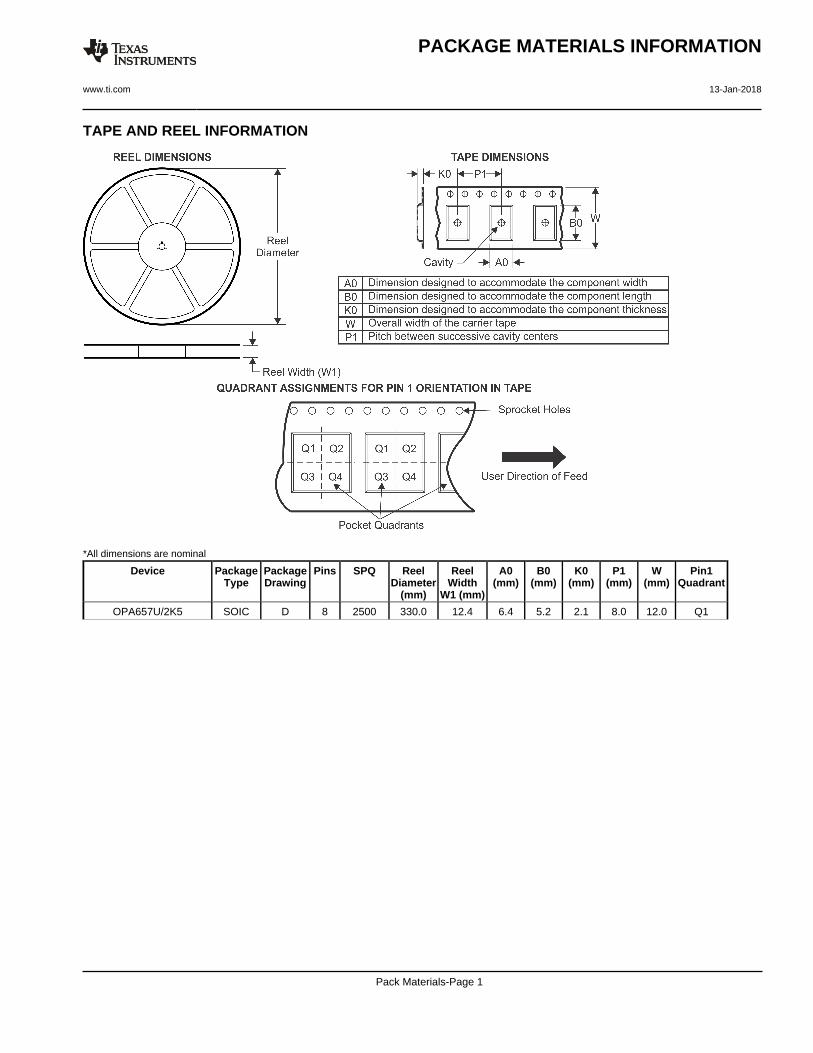
TAPE AND REEL INFORMATION
*All dimensions are nominal
Device PackageType
PackageDrawing
Pins SPQ ReelDiameter
(mm)
ReelWidth
W1 (mm)
A0(mm)
B0(mm)
K0(mm)
P1(mm)
W(mm)
Pin1Quadrant
OPA657U/2K5 SOIC D 8 2500 330.0 12.4 6.4 5.2 2.1 8.0 12.0 Q1
PACKAGE MATERIALS INFORMATION
www.ti.com 13-Jan-2018
Pack Materials-Page 1
*All dimensions are nominal
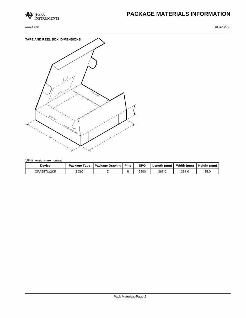
Device Package Type Package Drawing Pins SPQ Length (mm) Width (mm) Height (mm)
OPA657U/2K5 SOIC D 8 2500 367.0 367.0 35.0
PACKAGE MATERIALS INFORMATION
www.ti.com 13-Jan-2018
Pack Materials-Page 2
www.ti.com
PACKAGE OUTLINE
C
TYP0.220.08
0.25
3.02.6
2X 0.95
1.9
1.45 MAX
TYP0.150.00
5X 0.50.3
TYP0.60.3
TYP80
1.9
A
3.052.75
B1.751.45
(1.1)
SOT-23 - 1.45 mm max heightDBV0005ASMALL OUTLINE TRANSISTOR
4214839/C 04/2017
NOTES: 1. All linear dimensions are in millimeters. Any dimensions in parenthesis are for reference only. Dimensioning and tolerancing per ASME Y14.5M.2. This drawing is subject to change without notice.3. Refernce JEDEC MO-178.
0.2 C A B
1
34
5
2
INDEX AREAPIN 1
GAGE PLANE
SEATING PLANE
0.1 C
SCALE 4.000
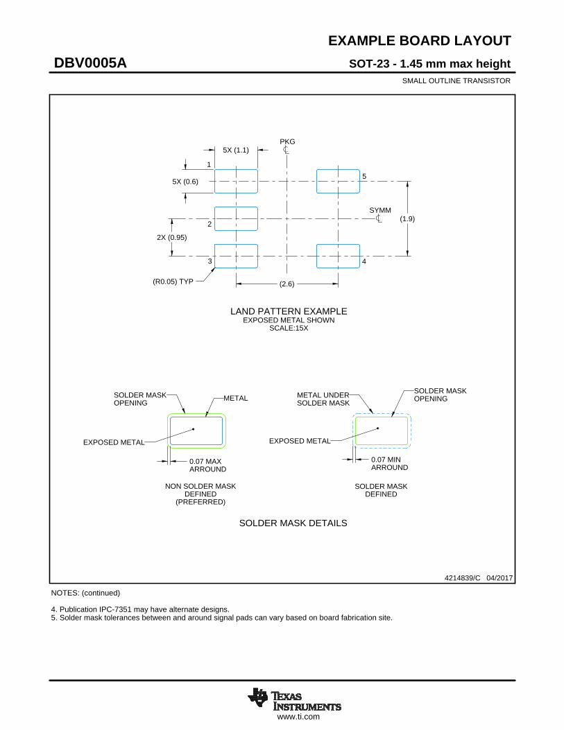
www.ti.com
EXAMPLE BOARD LAYOUT
0.07 MAXARROUND
0.07 MINARROUND
5X (1.1)
5X (0.6)
(2.6)
(1.9)
2X (0.95)
(R0.05) TYP
4214839/C 04/2017
SOT-23 - 1.45 mm max heightDBV0005ASMALL OUTLINE TRANSISTOR
NOTES: (continued) 4. Publication IPC-7351 may have alternate designs. 5. Solder mask tolerances between and around signal pads can vary based on board fabrication site.
SYMM
LAND PATTERN EXAMPLEEXPOSED METAL SHOWN
SCALE:15X
PKG
1
3 4
5
2
SOLDER MASKOPENINGMETAL UNDER
SOLDER MASK
SOLDER MASKDEFINED
EXPOSED METAL
METALSOLDER MASKOPENING
NON SOLDER MASKDEFINED
(PREFERRED)
SOLDER MASK DETAILS
EXPOSED METAL
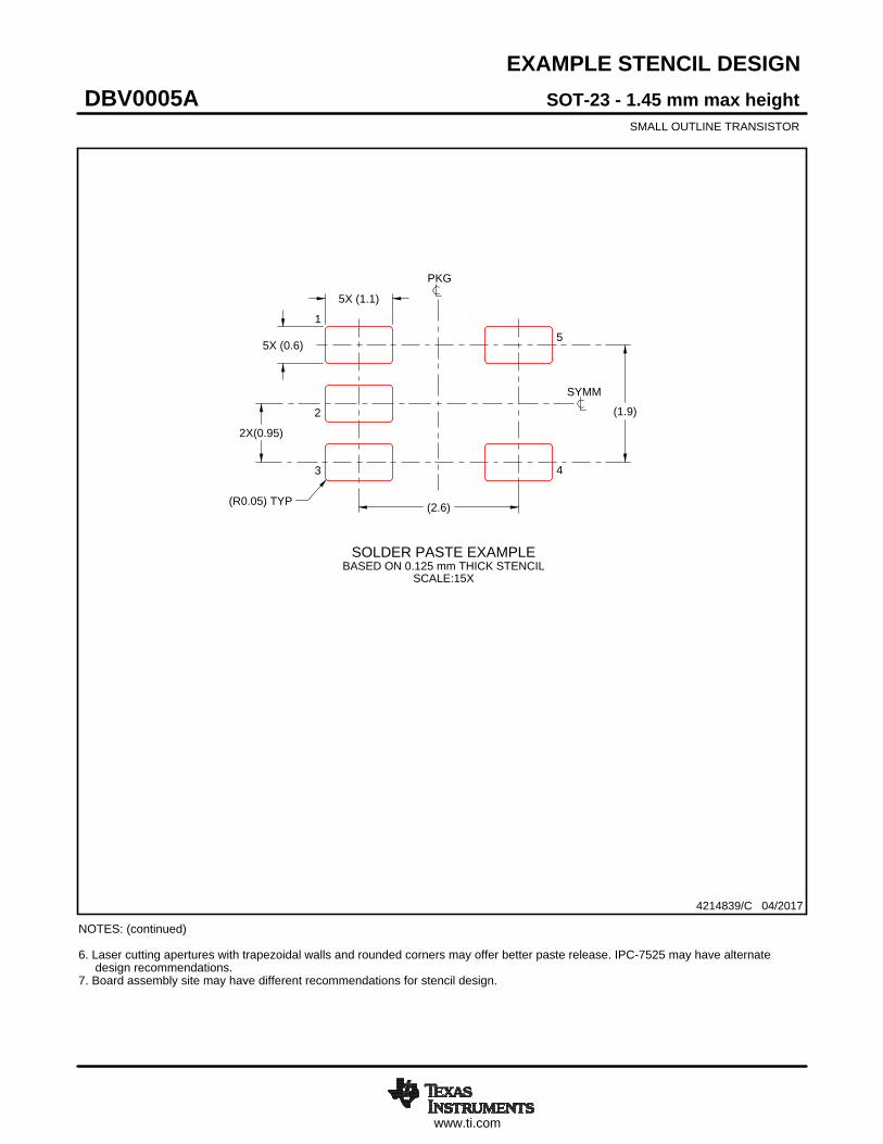
www.ti.com
EXAMPLE STENCIL DESIGN
(2.6)
(1.9)
2X(0.95)
5X (1.1)
5X (0.6)
(R0.05) TYP
SOT-23 - 1.45 mm max heightDBV0005ASMALL OUTLINE TRANSISTOR
4214839/C 04/2017
NOTES: (continued) 6. Laser cutting apertures with trapezoidal walls and rounded corners may offer better paste release. IPC-7525 may have alternate design recommendations. 7. Board assembly site may have different recommendations for stencil design.
SOLDER PASTE EXAMPLEBASED ON 0.125 mm THICK STENCIL
SCALE:15X
SYMM
PKG
1
3 4
5
2

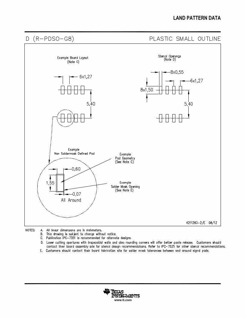
IMPORTANT NOTICE
Texas Instruments Incorporated (TI) reserves the right to make corrections, enhancements, improvements and other changes to itssemiconductor products and services per JESD46, latest issue, and to discontinue any product or service per JESD48, latest issue. Buyersshould obtain the latest relevant information before placing orders and should verify that such information is current and complete.TI’s published terms of sale for semiconductor products (http://www.ti.com/sc/docs/stdterms.htm) apply to the sale of packaged integratedcircuit products that TI has qualified and released to market. Additional terms may apply to the use or sale of other types of TI products andservices.Reproduction of significant portions of TI information in TI data sheets is permissible only if reproduction is without alteration and isaccompanied by all associated warranties, conditions, limitations, and notices. TI is not responsible or liable for such reproduceddocumentation. Information of third parties may be subject to additional restrictions. Resale of TI products or services with statementsdifferent from or beyond the parameters stated by TI for that product or service voids all express and any implied warranties for theassociated TI product or service and is an unfair and deceptive business practice. TI is not responsible or liable for any such statements.Buyers and others who are developing systems that incorporate TI products (collectively, “Designers”) understand and agree that Designersremain responsible for using their independent analysis, evaluation and judgment in designing their applications and that Designers havefull and exclusive responsibility to assure the safety of Designers' applications and compliance of their applications (and of all TI productsused in or for Designers’ applications) with all applicable regulations, laws and other applicable requirements. Designer represents that, withrespect to their applications, Designer has all the necessary expertise to create and implement safeguards that (1) anticipate dangerousconsequences of failures, (2) monitor failures and their consequences, and (3) lessen the likelihood of failures that might cause harm andtake appropriate actions. Designer agrees that prior to using or distributing any applications that include TI products, Designer willthoroughly test such applications and the functionality of such TI products as used in such applications.TI’s provision of technical, application or other design advice, quality characterization, reliability data or other services or information,including, but not limited to, reference designs and materials relating to evaluation modules, (collectively, “TI Resources”) are intended toassist designers who are developing applications that incorporate TI products; by downloading, accessing or using TI Resources in anyway, Designer (individually or, if Designer is acting on behalf of a company, Designer’s company) agrees to use any particular TI Resourcesolely for this purpose and subject to the terms of this Notice.TI’s provision of TI Resources does not expand or otherwise alter TI’s applicable published warranties or warranty disclaimers for TIproducts, and no additional obligations or liabilities arise from TI providing such TI Resources. TI reserves the right to make corrections,enhancements, improvements and other changes to its TI Resources. TI has not conducted any testing other than that specificallydescribed in the published documentation for a particular TI Resource.Designer is authorized to use, copy and modify any individual TI Resource only in connection with the development of applications thatinclude the TI product(s) identified in such TI Resource. NO OTHER LICENSE, EXPRESS OR IMPLIED, BY ESTOPPEL OR OTHERWISETO ANY OTHER TI INTELLECTUAL PROPERTY RIGHT, AND NO LICENSE TO ANY TECHNOLOGY OR INTELLECTUAL PROPERTYRIGHT OF TI OR ANY THIRD PARTY IS GRANTED HEREIN, including but not limited to any patent right, copyright, mask work right, orother intellectual property right relating to any combination, machine, or process in which TI products or services are used. Informationregarding or referencing third-party products or services does not constitute a license to use such products or services, or a warranty orendorsement thereof. Use of TI Resources may require a license from a third party under the patents or other intellectual property of thethird party, or a license from TI under the patents or other intellectual property of TI.TI RESOURCES ARE PROVIDED “AS IS” AND WITH ALL FAULTS. TI DISCLAIMS ALL OTHER WARRANTIES ORREPRESENTATIONS, EXPRESS OR IMPLIED, REGARDING RESOURCES OR USE THEREOF, INCLUDING BUT NOT LIMITED TOACCURACY OR COMPLETENESS, TITLE, ANY EPIDEMIC FAILURE WARRANTY AND ANY IMPLIED WARRANTIES OFMERCHANTABILITY, FITNESS FOR A PARTICULAR PURPOSE, AND NON-INFRINGEMENT OF ANY THIRD PARTY INTELLECTUALPROPERTY RIGHTS. TI SHALL NOT BE LIABLE FOR AND SHALL NOT DEFEND OR INDEMNIFY DESIGNER AGAINST ANY CLAIM,INCLUDING BUT NOT LIMITED TO ANY INFRINGEMENT CLAIM THAT RELATES TO OR IS BASED ON ANY COMBINATION OFPRODUCTS EVEN IF DESCRIBED IN TI RESOURCES OR OTHERWISE. IN NO EVENT SHALL TI BE LIABLE FOR ANY ACTUAL,DIRECT, SPECIAL, COLLATERAL, INDIRECT, PUNITIVE, INCIDENTAL, CONSEQUENTIAL OR EXEMPLARY DAMAGES INCONNECTION WITH OR ARISING OUT OF TI RESOURCES OR USE THEREOF, AND REGARDLESS OF WHETHER TI HAS BEENADVISED OF THE POSSIBILITY OF SUCH DAMAGES.Unless TI has explicitly designated an individual product as meeting the requirements of a particular industry standard (e.g., ISO/TS 16949and ISO 26262), TI is not responsible for any failure to meet such industry standard requirements.Where TI specifically promotes products as facilitating functional safety or as compliant with industry functional safety standards, suchproducts are intended to help enable customers to design and create their own applications that meet applicable functional safety standardsand requirements. Using products in an application does not by itself establish any safety features in the application. Designers mustensure compliance with safety-related requirements and standards applicable to their applications. Designer may not use any TI products inlife-critical medical equipment unless authorized officers of the parties have executed a special contract specifically governing such use.Life-critical medical equipment is medical equipment where failure of such equipment would cause serious bodily injury or death (e.g., lifesupport, pacemakers, defibrillators, heart pumps, neurostimulators, and implantables). Such equipment includes, without limitation, allmedical devices identified by the U.S. Food and Drug Administration as Class III devices and equivalent classifications outside the U.S.TI may expressly designate certain products as completing a particular qualification (e.g., Q100, Military Grade, or Enhanced Product).Designers agree that it has the necessary expertise to select the product with the appropriate qualification designation for their applicationsand that proper product selection is at Designers’ own risk. Designers are solely responsible for compliance with all legal and regulatoryrequirements in connection with such selection.Designer will fully indemnify TI and its representatives against any damages, costs, losses, and/or liabilities arising out of Designer’s non-compliance with the terms and provisions of this Notice.
Mailing Address: Texas Instruments, Post Office Box 655303, Dallas, Texas 75265Copyright © 2018, Texas Instruments Incorporated