Embed Size (px)
Citation preview
OPEN Lab Prof. Sorger
Volker Sorger
14th NSF-Korea Nanotechnology Forum 2017
aJ/bit Modulators and Photonic Neuromorphic Computing
OPEN Lab Prof. Sorger
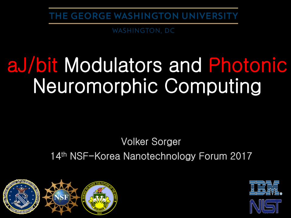
Orthogonal Physics Enabled Nanophotonics (OPEN) lab
compared to any photonic (non-plasmonic) mode and cavity structures where any placement of the metallic contact
close to the optical mode will introduce intolerable losses. This is different for our plasmonic mode, which is
inherently lossy, but the polaritonic (matter-like) mode allows to scale-down the device into a few micrometer small
device (a reduction of a factor of 100) compared to traveling-wave Silicon-based modulators. This ‘in-the-device-
basing’, as suppose to biasing the device few to 10’s of micrometer away from the active region. As such, the overall
design allows for a more compact overall footprint. Lastly, reducing the dielectric thickness (tox = 5 nm), improves the
electrostatics enabling a sub-1 Volt modulation performance. Despite this increasing the capacitance, the lower Rc and
small device area (5 mm2) the energy consumption is relatively low 18 fJ/bit. However, this can be further improved by
only biasing the device in the steepest region of the transfer function (e.g. 0-0.3V) for a small-signal modulation, and
narrowing the waveguide width from (currently 1 mm) to a SOI diffraction-limited waveguide width of 250 nm
reducing the E/bit to low 160aJ (Fig. 1d).
In summary, we have experimentally shown a graphene-based silicon-photonics integrated electro-absorption
modulator operating at telecom frequencies. Utilizing a hybrid-photon-plasmon modes high group index, field-
concentration to increase the optical overlap factor with the thin graphene active material, and improving the
electrostatics by reducing the gate oxide allows for a steep switching transfer function to enable sub-1 Volt
modulation, which has positive impacts on energy-efficiency. Further improvements allow for a 160aJ/bit efficient
modulator using this approach platform, thus paving the way for next-generation nanophotonics devices [13]. !
References [1] R. A. Soref, D. L. McDaniel, B. R. Bennett, “Guided-Wave Intensity Modulators Using Amplitude and-Phase Perturbations”
IEEE Journal of Lightwave Technology, vol. 6, no. 3, (1988).
[2] K. Liu, S. Sun, A. Majumdar, V. J. Sorger, “Fundamental Scaling Laws in Nanophotonics” Sci. Rep., 6, 37419 (2016).
[3] S. K. Pickus, S. Khan, C. Ye, Z. Li, and V. J. Sorger, “Silicon Plasmon Modulators: Breaking Photonic Limits” IEEE Phot.
Soc., 27, 6 (2013).
[4] M. Liu, X. Yin, E. Ulin-Avila, B. Geng, T. Zentgraf, L. Ju, F. Wang, and X. Zhang, “A graphene-based broadband optical
modulator,” Nature, vol. 474, no. 7349, pp. 64–67, (2011).
[5] M. Liu, X. Yin and X. Zhang, "Double-Layer Graphene Optical Modulator", Nano Letters, 12, no. 3, pp. 1482-1485, (2012).
[6] C. Ye, S. Khan, Z. R. Li, E. Simsek, V. J. Sorger (2014). “λ-size ITO and graphene-based electro-optic modulators on
SOI”. Selected Topics in Quantum Electronics, IEEE Journal of, 20(4), 40-49 (2014).![7] C. Ye, K. Liu, R. Soref, V. J. Sorger, “3-Waveguide 2x2 Plasmonic Electro-optic Switch” Nanophot., 4, 1, pp. 261-268 (2015).
[8] Z. Ma, M. Tahersima, S. Khan, V. J. Sorger, IEEE J. Sel. Topics in Quantum Electronics, 23(1), 3400208 (2017).
[9] R.Amin, C.Suer, Z.Ma, J. B. Khurgin, R. Agarwal, V. J. Sorger, “Active Material, Optical Mode and Cavity Impact on electro-
optic Modulation Performance”, arXiv:1612.02494, (2017)
[10] V. J. Sorger, R. Ma, C. Huang, Z. Li, M. Liu, and X. Zhang, "Graphene, Plasmonic and Silicon Optical Modulators,"
Conference on Lasers and Electro-Optics - IQEC,OSA, (2013).
[11] Z. Ma, Z. Li, K. Liu, C. Ye, V. J. Sorger, “Indium-Tin-Oxide for High-performance Electro-optic Modulation”, Nanophot., 4, 1
(2015).
[12] Ansell, D. et al. Hybrid graphene plasmonic waveguide modulators. Nature Commun. 6, 8846 (2015). [13] A. Fratalocchi, C. M Dodson, R. Zia, P. Genevet, et al. “Nano-optics gets practical”, Nature Nanotech. 10, 11-15 (2015).
Figure 1. a, Schematic of a hybrid-photon-plasmon
graphene-based electro-absorption modulator. The
modulation mechanism is based on Pauli-blocking upon
gating the Fermi level of graphene. b, Silicon waveguide-
integrated modulator. A cw laser (l = 1.55 mm) is fiber
coupled into the SOI waveguide via grating couplers.
Device length, L = 8 mm, tox = 5 nm. c, Electric field
density across the active MOS region of the modulator
showing an enhanced field strength coinciding with the
active graphene layer. This improves the optical overlap
factor by about 25%. Taking into consideration the grain
boundaries introduced during the metal deposited creates
in-plane field vectors inside the graphene layer. d
Modulator transfer function; normalized modulation depth
at different drive voltages (VD). The modulator
performance yields a high extinction ratio of 0.25dB/mm,
due to the combination of the plasmonic MOS mode
enhancing the electroabsorption in the active region (see
text for details).
!
Modulator
(i) (ii)
(iii) (iv)bias
input
output
Electro-OpticNonlinearity
ElectronicNonlinearity
pump
output
input
bias
output
input
output
pump
input
inputs
(c)
T(λ) output
input
t t t
λ1 λ2 λ3 λ1 λ2 λ3 λ4
photo-detector
spectralfilter
I(t) I(t) i(t) I(t)
t
weights summation nonlinearity output
(a)
(b)
!x1
x2
x3
w1
w2
w3
x⌃
f (x⌃ )
X
i
wi x ix4
modulator/laser
Laserelectrical wire
lightwave
Atto-Joule Optoelectronics
Photonic Functions
Analogue Computing
Today
Sorger, Zhang lab, Nature Photonics (2008) Sorger, Zhang lab, Nature (2009) Sorger lab , IEEE Photonics (2013) Sorger lab, Altug lab, Nature Nanotech. (2015) Sorger lab, Majumdar Lab, Sci. Reports (2016) Sorger lab, Optics Letters (2016) Sorger lab, IEEE STQE (2014 & 2017)
Sorger lab, IEEE Photonics (2015) Sorger lab, Nanophotonics (2016) Sorger lab, Optics Letters (2016) Sorger lab, El-Ghazawi lab, IPCC (2017) Sorger lab, El-Ghazawi lab, Mircoprocess. & MS (2017) Sorger lab, Frontiers in Optics (2017)
Sorger lab, Nanophotonics (2017) Sorger Lab, Grace lab, Biofabrication (2017) Sorger lab, IEEE Rebooting Computing (2017) Prucnal lab, Sorger lab, (in preparation)
OPEN Lab Prof. Sorger OPEN Lab
Prof. Sorger
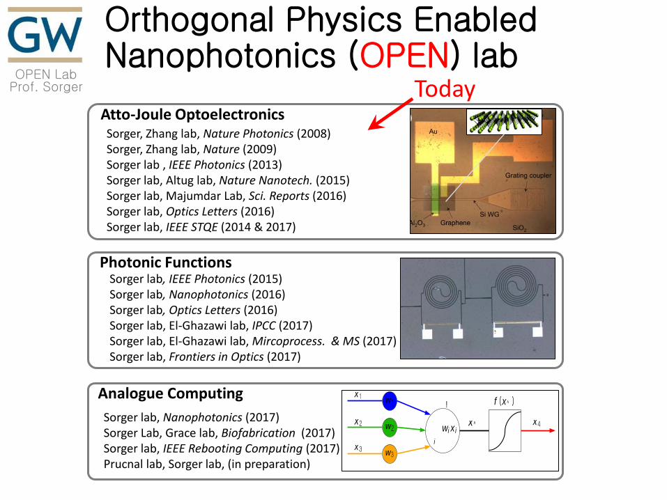
5cm x 1cm
Modulators = Optical Transistors
EO Modulator
(=SS@FET)
OPEN Lab Prof. Sorger
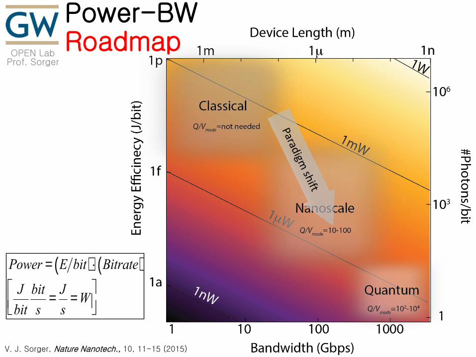
Power-BW Roadmap
V. J. Sorger, Nature Nanotech., 10, 11-15 (2015)
Power = E bit( ) × Bitrate( )
J
bit
bit
s=
J
s= W
é
ëê
ù
ûú
OPEN Lab Prof. Sorger
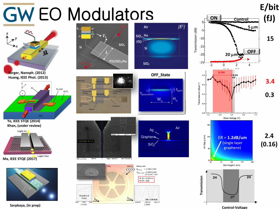
EO Modulators
Sorger, Nanoph. (2012) Huang, IEEE Phot. (2013)
Ye, IEEE STQE (2014) Khan, (under review)
Ma, IEEE STQE (2017)
LASER &PHOTONICSREVIEWS
Vol. 9 | March 2015
Review and perspective on ultra-fast wavelength-size electro-optic modulators
Ke Liu, Chenran Ye, Sikandar Khan, Volker J. Sorger
www.lpr-journal.org Vol. 9 | March 2015 www.lpr-journal.org
Selective switching of individual multipole resonances in single dielectric nanoparticles
Pawel Wozniak, Peter Banzer, Gerd Leuchs
LASER &PHOTONICSREVIEWS
LPOR_9_2_cover.indd 2 11/03/15 5:05 PM
Sarpkaya, (in prep)
Grating period: 1um Fill Factor: 50%
Slot Gap < 50nm achieved Single EBL Exposure
ER = 1.2dB/um (single layer graphene)
ON
OFF 20 mm
5 mm
Control
2H 2H
1T’ Tr
ansm
issi
on
Control-Voltage
15 15
E/bit (fJ)
3.4
0.3
15
2.4 (0.16)
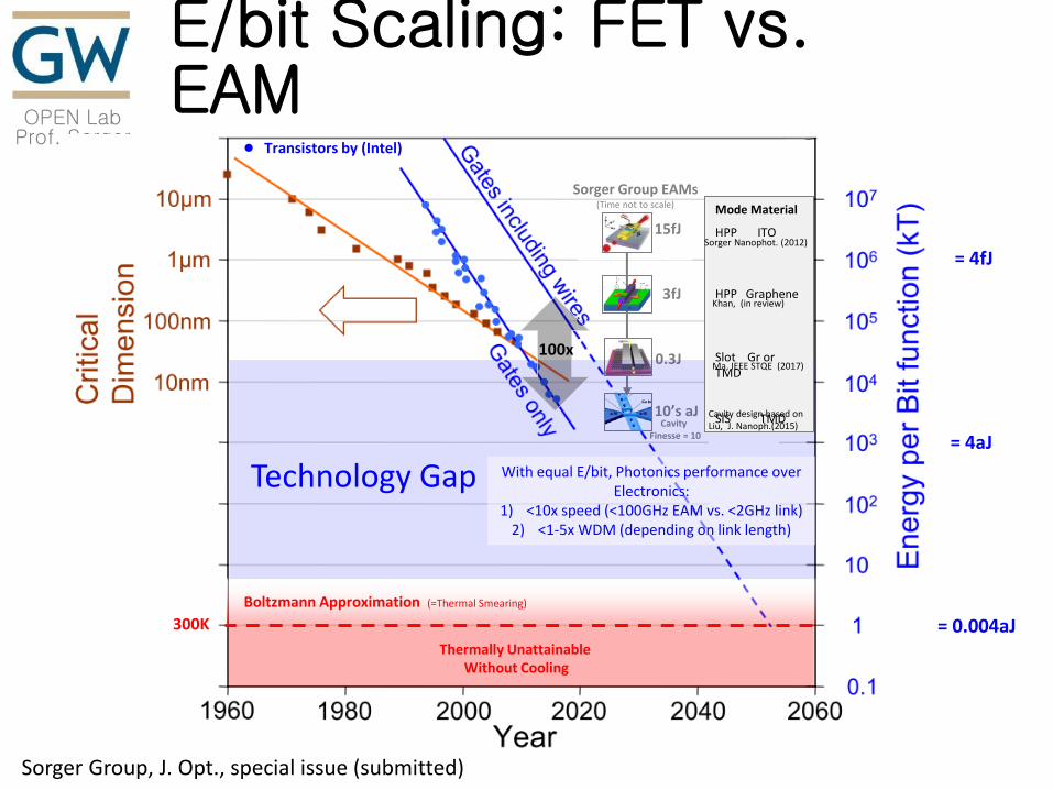
OPEN Lab Prof. Sorger
E/bit Scaling: FET vs. EAM
300K = 0.004aJ
= 4aJ
= 4fJ
15fJ
3fJ
0.3J
Boltzmann Approximation (=Thermal Smearing)
Sorger Group EAMs (Time not to scale)
10’s aJ Cavity
Finesse = 10
Mode Material
HPP ITO
HPP Graphene Slot Gr or TMD
SIS TMD
Technology Gap With equal E/bit, Photonics performance over Electronics:
1) <10x speed (<100GHz EAM vs. <2GHz link) 2) <1-5x WDM (depending on link length)
Sorger Nanophot. (2012)
Khan, (in review)
Ma, IEEE STQE (2017)
Cavity design based on Liu, J. Nanoph.(2015)
•
Thermally Unattainable Without Cooling
Transistors by (Intel)
Sorger Group, J. Opt., special issue (submitted)
100x
OPEN Lab Prof. Sorger
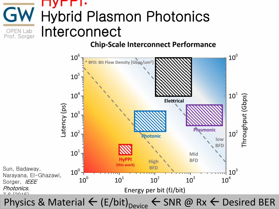
HyPPI: Hybrid Plasmon Photonics Interconnect
Sun, Badaway, Narayana, El-Ghazawi, Sorger, IEEE Photonics, 7,6 (2015).
High BFD
Mid BFD
low BFD
Electrical
Plasmonic Photonic
HyPPI (this work)
* BFD: Bit Flow Density [Gbps/um2]
Physics & Material (E/bit)Device SNR @ Rx Desired BER
OPEN Lab Prof. Sorger
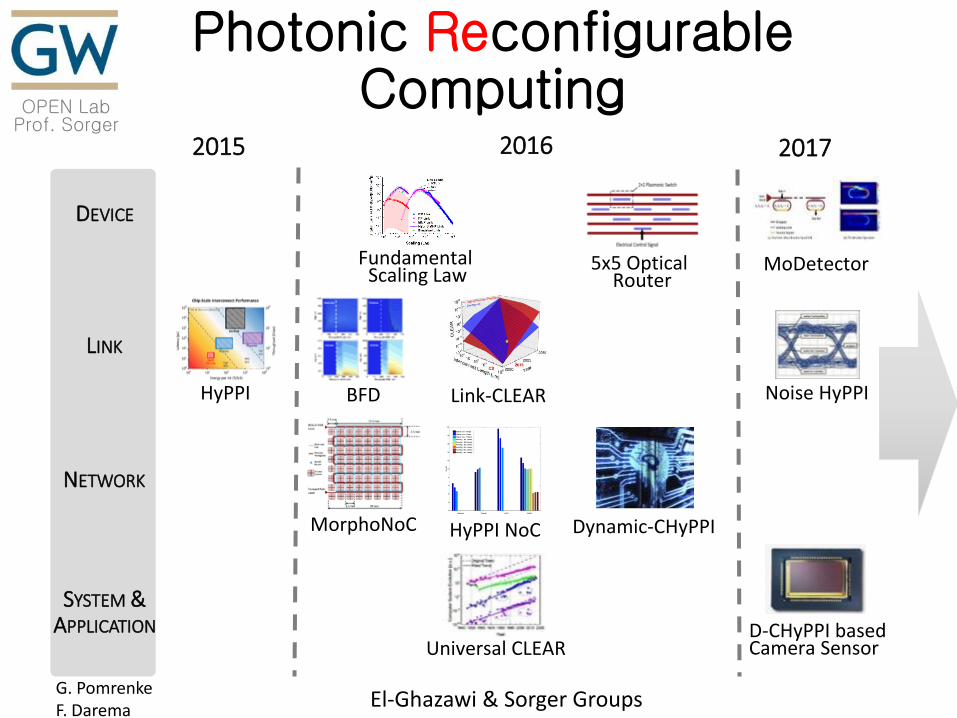
Photonic Reconfigurable Computing
2015 2016 2017
MorphoNoC
DEVICE
LINK
NETWORK
SYSTEM & APPLICATION
HyPPI BFD
MoDetector
Universal CLEAR
For P
eer Review
Fig. 2 Capability-to-Length-Energy-Area-Resistance (CLEAR) based performance-cost comparison
between electrical (red) and hybrid photon-plasmon (blue) on-chip interconnect links as a function of link
length and technology evolution time. The chip scale (CS = 1 cm) link length and current year (2016) are
denoted in red. The following models are deployed; a) A capacity-area model based on the number of
transistors and on-chip optical devices, which can be regarded as the original Moore’s Law model; b) An
energy efficiency model is derived based on Koomey’s law, which is bounded by the kBT ln(2) ≈ 2.75zJ/bit,
Landauer limit (kB is the Boltzmann constant; T is the temperature); c) A the economic resistance model
based on technology-experience models and at the year 2016, the electronic link cost less than one billionth
to one millionth of the cost of the hybrid link; and d) A model for parallelism (after year 2006) capturing
multi-core architecture and the limitation from ‘dark’ silicon concepts in electrical link interconnects. The
yellow data point represents the actual CMOS silicon photonic chip that IBM fabricated in 2015.
Page 5 of 5 Spectrum
Link-CLEAR
Dynamic-CHyPPI HyPPI NoC
D-CHyPPI based Camera Sensor
Noise HyPPI
5x5 Optical Router
Fundamental Scaling Law
G. Pomrenke F. Darema
El-Ghazawi & Sorger Groups
OPEN Lab Prof. Sorger
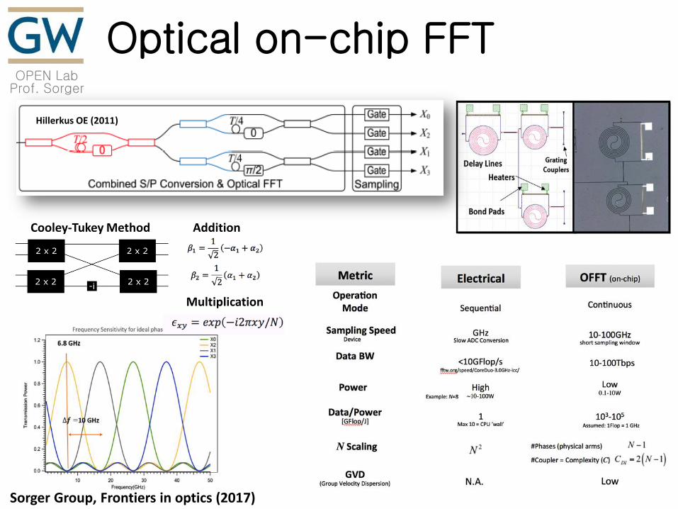
Optical on-chip FFT
Hillerkus OE (2011)
Cooley-Tukey Method Addition
Multiplication
Sorger Group, Frontiers in optics (2017)
OPEN Lab Prof. Sorger
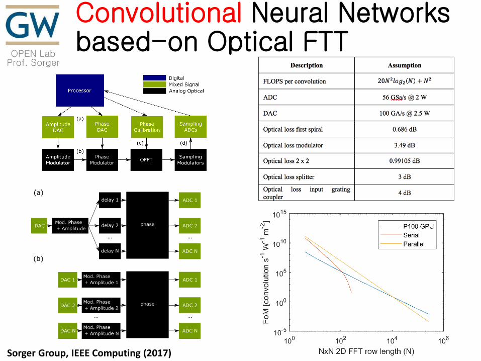
Convolutional Neural Networks based-on Optical FTT
Sorger Group, IEEE Computing (2017)
OPEN Lab Prof. Sorger
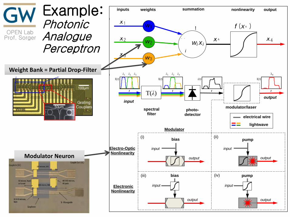
Example: Photonic Analogue Perceptron
Modulator
(i) (ii)
(iii) (iv)bias
input
output
Electro-OpticNonlinearity
ElectronicNonlinearity
pump
output
input
bias
output
input
output
pump
input
inputs
(c)
T(λ) output
input
t t t
λ1 λ2 λ3 λ1 λ2 λ3 λ4
photo-detector
spectralfilter
I(t) I(t) i(t) I(t)
t
weights summation nonlinearity output
(a)
(b)
!x1
x2
x3
w1
w2
w3
x⌃
f (x⌃ )
X
i
wi x ix4
modulator/laser
Laserelectrical wire
lightwave
Weight Bank = Partial Drop-Filter
Modulator Neuron
OPEN Lab Prof. Sorger
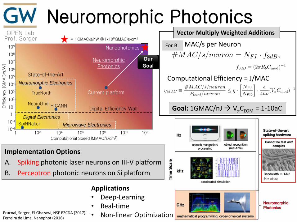
Neuromorphic Photonics
Prucnal, Sorger, El-Ghazawi, NSF E2CDA (2017) Ferreira de Lima, Nanophot (2016)
Nanophotonic Neuromorphic Computing
1 Introduction
TrueNorth
NeuroGrid HICANN
Neuromorphic Electronics
Current platform
Digital Electronics
Digital Efficiency Wall
State-of-the-Art
SpiNNaker Microwave Electronics
Neuromorphic Photonics
102
103
104
105
106
107
108
1
10
10-1
Effic
iency (G
MAC
/s/W
)
10-2
Computational Speed (MMAC/s/cm2)
1021 104 106 108 1010
109
1011
Nanophotonics
= 1 GMAC/s/nW @ 1x10⁸ GMAC/s/cm2
This Project
Figure 1: Comparison of computational energy effi-
ciency and processing speed between existing elec-
tronic neuromorphic demonstrations and our proposed
programmable photonic platform meeting the NSF–SRC
challenge of 1 Giga-MAC/s/nW.
The gap between current computing capabilities and
current computing needs is widening due to the limitations
conventional, microelectronic processors. This insufficiency
is increasingly apparent in problems involving complex sys-
tems [1, 2], big data [3, 4], or real-time requirements [5].
In only some respects, processor performance has kept
pace with the expectations of Moore’s law; however, the ef-
ficiency of elemental multiply-accumulate (MAC) operations
has plateaued [6,7]at about 10 GigaMACs per second per
Watt (see digital efficiency wall in Fig. 1). This represents a
factor of only ⇠2 over the past 14 years. It is no longer pos-
sible for microelectronics to maintain previous rates of pro-
cessor evolution in speed, efficiency, and generality [8–10].
There is also a consensus that centralized, universal von-
Neumann architectures employed by conventional comput-
ers are no longer capable of being the one-size-fits-all ap-
proach to computing problems.
50µm
Broadcast Loop
Current Prototype:Silicon Photonic Chip (without EOM)
Photonic Neuron (EOM)
50µm
Microring Weight Bank
Broadcast-and-WeightAssembly
Small-world NetworkProcessing Stage
Interconnected PICsProcessing Networks
Processing Network Node
Primitive
Weights(Mircorings)
Neuron (EOM)
Figure 2: (Top) Scalable, programmable complex analog photonic processor. Hi-
erarchical architecture at different scales—from individual spike primitives to in-
terconnected complex photonic integrated circuits. (Bottom) Proposed computa-
tional primitive i.e. photonic neuron and current prototype of an integrated pho-
tonic neural network on silicon photonics chip.
Non-von-Neumann computing ar-
chitectures have been developed to
outperform in particular metrics, but
often at the expense of the other met-
rics (Section 2). Hardware devel-
oped for deep learning excels in ef-
ficiency at the cost of generality. Dig-
ital neuromorphic architectures offer
the generality of neural networks, but
at the expense of MAC efficiency.
Forays into unconventional comput-
ing have, so far, only been partially
successful because of the physical
limitations posed by metal intercon-
nects [11–13] and digital weighted
addition. Breaking the limitations
inherent in conventional microelec-
tronic computers will require a cross-
disciplinary approach to use new
physical phenomena and new pro-
cessing models.
Photonics can resolve the limita-
tions inherent in the digital MAC op-
eration and those of microelectronic
interconnects. Photonic weighted
addition, the analog photonic equivalent of a MAC, offers MAC energy consumption that does not tradeoff with
MAC speed. Photonic physics does not provide simple mechanisms to maintain logic levels in a way that is
cascadable and robust [14]. On the other hand, photonic phenomena can be employed to implement analog
weighted addition with unmatched speed, efficiency, and scalability (Section 3). Furthermore, photonic transport
physics can support massively distributed interconnections with commensurate performance.
The proposed program represents a vertically integrated approach to creating extremely high-performance
processors based on photonics (Figs. 1 and 2). In Sec. 4.1, we propose to investigate new devices, archi-
tectures, and evaluation standards, all of which must work in concert for the success of the program. Device
1
Implementation Options
A. Spiking photonic laser neurons on III-V platform
B. Perceptron photonic neurons on Si platform
Our Goal
MAC/s per Neuron
Computational Efficiency = J/MAC
Goal: 1GMAC/nJ VpCEOM = 1-10aC
For B.
Applications • Deep-Learning • Real-time • Non-linear Optimization
Vector Multiply Weighted Additions
OPEN Lab Prof. Sorger
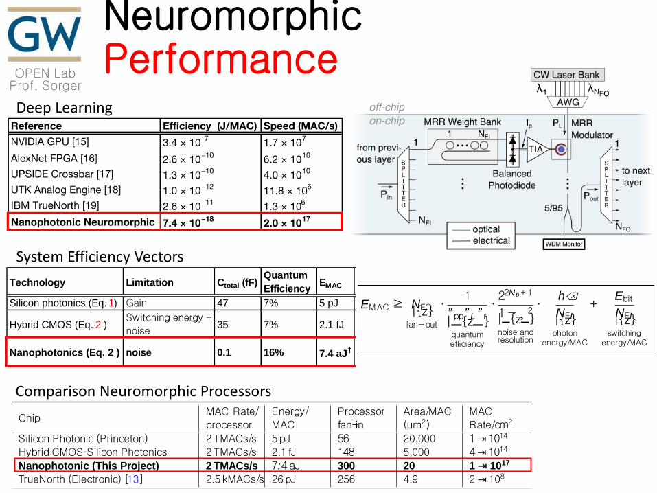
Neuromorphic Performance
Deep Learning
Table 1: Comparison Between Different Neuromorphic Processors
ChipMAC Rate/
processor
Energy/
MAC
Processor
fan-in
Area/MAC
(µm2)
MAC
Rate/cm2
Silicon Photonic (Princeton) 2TMACs/s 5pJ 56 20,000 1⇥1014
Hybrid CMOS-Silicon Photonics 2TMACs/s 2.1 fJ 148 5,000 4⇥1014
Nanophotonic (This Project) 2 TMACs/s 7:4aJ 300 20 1 ⇥ 1017
TrueNorth (Electronic) [13] 2.5kMACs/s 26pJ 256 4.9 2⇥108
A table including performance metrics for various development stages of the proposed platform, and comparison to a popular
electronic implementation. 1 TMAC refers to 1⇥1012 MACs. The energy per MAC for TrueNorth was estimated by dividing
wall-plug power to number of neurons and to operational MAC rate per processor. The MAC Rate /cm2 was computed for the
photonic case assuming a 20GHz bandwidth for each node. All numbers include overheads in terms of footprint and area.
Density, Bandwidth and Speed Beyond energy efficiency, we evaluated how neuromorphic photonics will prac-
tically scale in density and speed. In Table 1, we have summarized the calculated metrics for the course of this
project, the MAC rate (per processor), energy per MAC (pJ), processor fan-in, and area per MAC. In the following
sections, we briefly discuss the physical effects that define these metrics.
Technology Limitation Ctotal (fF)Quantum
EfficiencyEMAC Notes
Silicon photonics (Eq. 1) Gain 47 7% 5 pJ Princeton
Hybrid CMOS (Eq. 2 )Switching energy +
noise35 7% 2.1 fJ
Nanophotonics (Eq. 2 ) noise 0.1 16% 7.4 aJ†
Figure 12: Efficiency estimations in different platforms. Silicon pho-
tonics (current technology). Hybrid CMOS (under research cur-
rently). Nanophotonic (next-generation silicon photonics + CMOS).
We assumed that NFO ⇡ NFI , with NFI on the order of 100. †Note:
Nanophotonic implementation requires high performance CMOS TIA:
power consumption less than 1µW while supporting a bandwidth of
more than 10GHz.
Number of Interconnects and Bandwidth The
network capacity is limited by two factors: (a)
the transform-limited bandwidth of the optical
transmission window, and (b) the finesse of op-
tical resonators utilized in weight banks. For ex-
ample, using a standard optical telecommunica-
tions band exceeding 4THz and 20GHz chan-
nels, we can expect >100 channels that each
node can receive. However, there are some en-
gineering challenges to reach that channel den-
sity. The finesse of the resonators must be
high enough to accommodate the 4THz band,
and the microrings must be engineered to have
transmission curves as packed as possible (cf. Fig. 5). Recent channel density studies [32]quantified analysis
for multiwavelength analog networks, and derived a limit of N 148 fan-in per PN. Using more advanced –-size,
nanophotonic cavities (i.e. photonic crystal defect state) could lead to higher Q filters and flatter resonances,
potentially increasing the channel account to 200.
MAC Unit Density Traditional photonic devices are diffraction-limited—i.e., devices and waveguides cannot
shrink much smaller than ⇠1µm2 in size. Although this number is much larger than seen in electronics (⇠5nm),
in digital architectures, many thousands of electronic transistors are needed to emulate simple mathematical or
floating point functions, which increases energy consumption and occupies space (cf. TrueNorth in Table 1). Uti-
lizing underlying physical phenomena to perform computations leads to 3–4x orders of magnitude improvements
in energy efficiency and information density (per area) in comparison.
MAC Rate Per Processor One of the most pronounced advantages of the nanophotonic platform is the speed
and bandwidths that it can achieve during operation. In digital systems, processing speed is bounded by the
clock rate, which puts an upper bound on the temporal resolution of digital information. The neuromorphic
photonic implementation avoids these limitations by using photonic interconnects together with electronic nodes
for nonlinear operations: optical signals surpass the bandwidth limitations of metal interconnects, while low-
power, analog electronic circuits have the potential to minimize (J/MAC) energy consumption to allow for more
scalability. Interconnects are optical, so the nodes are small enough to avoid transmission line effects.
Typical waveguide lengths on-chip are <1mm (i.e., <10ps time-of-flight in silicon), and typical resonator effects
have similar time constants. Thus, delays of the signal are no more than tens of picoseconds. Optoelectronic
components (such as photodetectors, modulators, or transimpedance amplifiers) in modern platforms such as
IMEC [68] can accept signals on the order of 20GHz to 30GHz. Since the optical response is much faster
than this range, optoelectronic circuits are the primary contribution to limitations in bandwidth. Considering both
bandwidth and latency together, the operating signal bandwidth can exceed >20GHz range.
9
System Efficiency Vectors
where ” L is the wall-plug-to-chip coupling efficiency of the laser source; ” pp, the total optical efficiency between
one optical stage and the next; ” r the photodiode’s quantum efficiency; NF O=NF I the ratio between fan-out and
fan-in, typically greater than 1; h⌫=e, the photon energy divided by electron’s charge; Vs, the inverse slope of the
modulator’s transmission curve; and, finally Cmod + CPD, the joint capacitances of the modulator and photodiode,
respectively. The laser pump power consumption by far dominates all others in this case, overcoming both
the noise and switching energy contributions to power consumption. The quantity Vs(Cmod + CPD) must be
minimized as much as possible, with capacitances on the order of attofarads to meet the energy efficiency
objective. This may be possible using the proposed modulator (Section 4.1) at very low temperatures (! 0K):
graphene, for example, experiences no carrier freeze-out, and its sensitivity ffen can be enhanced proportional
to the temperature ffen = T=T0. However, one must also consider the energy burden of cryogenics, which will
largely offset these advantages. Instead, we can take use electronic amplification to tackle this problem at room
temperature: namely, the use of an active CMOS-based trans-impedance amplifier (TIA).
Figure 10: PN signal pathway between two neural layers in
feedforward configuration.
Hybrid CMOS-Silicon Photonics An active trans-
impedance amplifier (TIA) serves several functions:
it can separate capacitive contributions of the pho-
todetector and modulator, and it also reduces the
impedances associated with each stage. That allows
us to effect a full voltage swing to the modulator even
if the current I p is low, bringing the pump power down
while maintaining cascadability.
There are two main limiting factors of signal power
in this link, namely, the shot noise at the photodetector
and TIA, and the resolution of the weight banks. The
combination of these two phenomena can be seen
in Fig. 11, and results in a noise-limited trade-off be-
tween low-power and bandwidth. With the power of
the lasers down to the noise-limit, the power con-
sumed by the switching energy of the modulator, Ebit , becomes more significant. The recalculated EMAC accounts
for both the laser energy consumption and the switching energy of the modulator.
EMAC ≥ NFO|{z}fan−out
·1
” pp” L ” r| {z }
quantumefficiency
·22Nb + 1
1− ¸ 2| {z }noise andresolution
·h⌫
NFI|{z}photon
energy/MAC
+Ebit
NFI|{z}switching
energy/MAC
(2)
Figure 11: SNR analysis considering both weight bank reso-
lution and noise cascadability requirements. The nonlinearity
factor of the modulator, ¸ , reduces the noise of the signal as it
travels through. This compares to transistors restoring the logic
voltage levels between gates. Therefore, the SNR of the signal
is limited above by how much the modulator can compensate
for shot noise accumulation. The signal must also match the
bit resolution of the MAC operation, Nb : SNR > 4Nb . That
imposes a lower limit on the SNR for a given bit resolution.
Equation (2) outlines the main vectors of improve-
ment for this project. For context, one attojoule per
MAC translates to EMAC⇠10h⌫. First, all the quantum
efficiencies need to be improved, namely, the photonic
link efficiency, ” pp; the laser wall-plug efficiency, ” L;
and the photodiode’s quantum efficiency, ” r. Second,
the modulator nonlinearity could be enhanced ¸ ! 0,
and the bit resolution, Nb of the neural network, lim-
ited. Finally, the modulator’s switching energy should
be minimized to sub-femtojoule levels, assuming a
fan-in number in the hundred.
Nanophotonics (This Project) To meet the NSF tar-
get, each MAC operation energy consumption must
be on the order of an attojoule. Figure 12 summa-
rizes the efficiency performance for the different fab
platforms discussed above. It shows that to achieve
attojoule-level energy efficiency, it is necessary toboth
cointegrate photonics with CMOS and bring better ef-
ficiencies with nanophotonic devices.
8
where ” L is the wall-plug-to-chip coupling efficiency of the laser source; ” pp, the total optical efficiency between
one optical stage and the next; ” r the photodiode’s quantum efficiency; NF O=NF I the ratio between fan-out and
fan-in, typically greater than 1; h⌫=e, the photon energy divided by electron’s charge; Vs, the inverse slope of the
modulator’s transmission curve; and, finally Cmod + CPD, the joint capacitances of the modulator and photodiode,
respectively. The laser pump power consumption by far dominates all others in this case, overcoming both
the noise and switching energy contributions to power consumption. The quantity Vs(Cmod + CPD) must be
minimized as much as possible, with capacitances on the order of attofarads to meet the energy efficiency
objective. This may be possible using the proposed modulator (Section 4.1) at very low temperatures (! 0K):
graphene, for example, experiences no carrier freeze-out, and its sensitivity ffen can be enhanced proportional
to the temperature ffen = T=T0. However, one must also consider the energy burden of cryogenics, which will
largely offset these advantages. Instead, we can take use electronic amplification to tackle this problem at room
temperature: namely, the use of an active CMOS-based trans-impedance amplifier (TIA).
Figure 10: PN signal pathway between two neural layers in
feedforward configuration.
Hybrid CMOS-Silicon Photonics An active trans-
impedance amplifier (TIA) serves several functions:
it can separate capacitive contributions of the pho-
todetector and modulator, and it also reduces the
impedances associated with each stage. That allows
us to effect a full voltage swing to the modulator even
if the current I p is low, bringing the pump power down
while maintaining cascadability.
There are two main limiting factors of signal power
in this link, namely, the shot noise at the photodetector
and TIA, and the resolution of the weight banks. The
combination of these two phenomena can be seen
in Fig. 11, and results in a noise-limited trade-off be-
tween low-power and bandwidth. With the power of
the lasers down to the noise-limit, the power con-
sumed by the switching energy of the modulator, Ebit , becomes more significant. The recalculated EMAC accounts
for both the laser energy consumption and the switching energy of the modulator.
EMAC ≥ NFO|{z}fan−out
·1
” pp” L ” r| {z }
quantumefficiency
·22Nb + 1
1− ¸ 2| {z }noise andresolution
·h⌫
NFI|{z}photon
energy/MAC
+Ebit
NFI|{z}switching
energy/MAC
(2)
Figure 11: SNR analysis considering both weight bank reso-
lution and noise cascadability requirements. The nonlinearity
factor of the modulator, ¸ , reduces the noise of the signal as it
travels through. This compares to transistors restoring the logic
voltage levels between gates. Therefore, the SNR of the signal
is limited above by how much the modulator can compensate
for shot noise accumulation. The signal must also match the
bit resolution of the MAC operation, Nb : SNR > 4Nb . That
imposes a lower limit on the SNR for a given bit resolution.
Equation (2) outlines the main vectors of improve-
ment for this project. For context, one attojoule per
MAC translates to EMAC⇠10h⌫. First, all the quantum
efficiencies need to be improved, namely, the photonic
link efficiency, ” pp; the laser wall-plug efficiency, ” L;
and the photodiode’s quantum efficiency, ” r. Second,
the modulator nonlinearity could be enhanced ¸ ! 0,
and the bit resolution, Nb of the neural network, lim-
ited. Finally, the modulator’s switching energy should
be minimized to sub-femtojoule levels, assuming a
fan-in number in the hundred.
Nanophotonics (This Project) To meet the NSF tar-
get, each MAC operation energy consumption must
be on the order of an attojoule. Figure 12 summa-
rizes the efficiency performance for the different fab
platforms discussed above. It shows that to achieve
attojoule-level energy efficiency, it is necessary to both
cointegrate photonics with CMOS and bring better ef-
ficiencies with nanophotonic devices.
8
Comparison Neuromorphic Processors
OPEN Lab Prof. Sorger
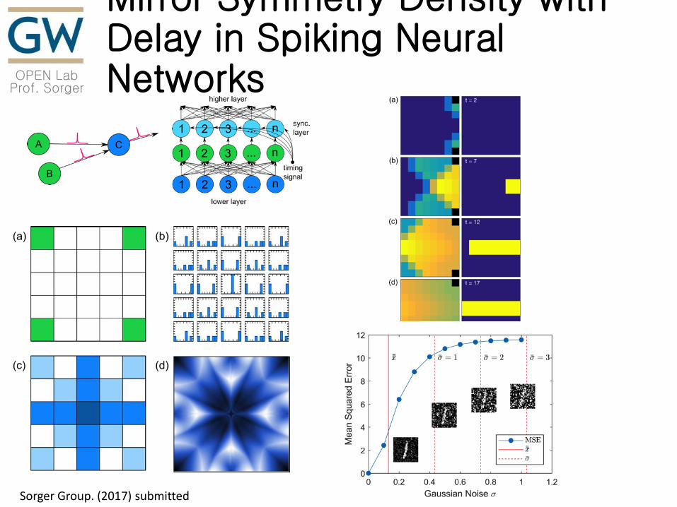
Mirror Symmetry Density with Delay in Spiking Neural Networks
Sorger Group. (2017) submitted
OPEN Lab Prof. Sorger
Prof. Volker Sorger sorger.seas.gwu.edu [email protected]
OPEN Sorger Team
Post Docs Grad Students U-grads Collaborators
Dr. I. Sarpkaya Dr. Ke Liu Dr. Hasan Goktas Dr. Elnaz Akbari
Mohammad Tahersima Sikandar Khan Matt Zhizhen Shuai Sun Jonathan George Rubab Amin Hani Nejadriahi Seyed Haghshenas Rohit Hemnani
D. D’Hemmecout T. Weinshel J. Crandall
Prof. Majumdar (UW) Prof. Agarwal (UPenn) Prof. Kimerling (MIT) Prof. Reed (Stanford) Prof. Bartels (UCR) Prof. Lee (KU) Prof. Prucnal (Princeton ) Prof. El Ghazawi (GWU) Dr. Sadana (IBM Watson) Prof. Cesare (NTU)