Embed Size (px)
Citation preview

Calhoun: The NPS Institutional Archive
Theses and Dissertations Thesis Collection
2014-12
Operational characteristics of an
SCR-based pulse generating circuit
Chang, Wing Chien Christopher
Monterey, California: Naval Postgraduate School
http://hdl.handle.net/10945/44535

NAVAL POSTGRADUATE
SCHOOL
MONTEREY, CALIFORNIA
THESIS
Approved for public release; distribution is unlimited
OPERATIONAL CHARACTERISTICS OF AN SCR-BASED PULSE GENERATING CIRCUIT
by
Wing Chien Christopher Chang
December 2014
Thesis Advisor: Gamani Karunasiri Co-Advisor: Fabio Alves

THIS PAGE INTENTIONALLY LEFT BLANK

REPORT DOCUMENTATION PAGE Form Approved OMB No. 0704-0188 Public reporting burden for this collection of information is estimated to average 1 hour per response, including the time for reviewing instruction, searching existing data sources, gathering and maintaining the data needed, and completing and reviewing the collection of information. Send comments regarding this burden estimate or any other aspect of this collection of information, including suggestions for reducing this burden, to Washington headquarters Services, Directorate for Information Operations and Reports, 1215 Jefferson Davis Highway, Suite 1204, Arlington, VA 22202-4302, and to the Office of Management and Budget, Paperwork Reduction Project (0704-0188) Washington DC 20503. 1. AGENCY USE ONLY (Leave blank)
2. REPORT DATE December 2014
3. REPORT TYPE AND DATES COVERED Master’s Thesis
4. TITLE AND SUBTITLE OPERATIONAL CHARACTERISTICS OF AN SCR-BASED PULSE GENERATING CIRCUIT
5. FUNDING NUMBERS
6. AUTHOR(S) Wing Chien Christopher Chang 7. PERFORMING ORGANIZATION NAME(S) AND ADDRESS(ES)
Naval Postgraduate School Monterey, CA 93943-5000
8. PERFORMING ORGANIZATION REPORT NUMBER
9. SPONSORING /MONITORING AGENCY NAME(S) AND ADDRESS(ES) N/A
10. SPONSORING/MONITORING AGENCY REPORT NUMBER
11. SUPPLEMENTARY NOTES The views expressed in this thesis are those of the author and do not reflect the official policy or position of the Department of Defense or the U.S. Government. IRB Protocol number ____N/A____.
12a. DISTRIBUTION / AVAILABILITY STATEMENT Approved for public release; distribution is unlimited
12b. DISTRIBUTION CODE
13. ABSTRACT (maximum 200 words) A commercial off-the-shelf silicon controlled rectifier (SCR) was connected in series with a parallel RC load under DC bias to produce self-terminating voltage pulses. The physics underlying the switching mechanism of the SCR in such a circuit was investigated and the values of load resistance and capacitance varied to ascertain their role on the pulse-generating capability of the circuit. When pulsing was successfully achieved, a reverse recovery current was always present to return the SCR from its “on” state to its “off” state. In addition, the regenerative process responsible for turning the SCR is through the avalanche multiplication of charge carriers within the device. This appeared to be independent of the mode of triggering, either by increasing the DC bias or using a current at the gate. Significantly, pulsing was discovered to be sustainable for a specific range of RC values that depends on the SCR’s intrinsic turn-off time. Specifically, it was found that without making modifications to the SCR itself, the minimum dead time achievable between pulses was essentially the turn-off time of the SCR. The findings of the research will help to design optimum SCR-based circuits for pulse mode detection of light and ionizing radiation without external amplification circuitry. 14. SUBJECT TERMS silicon controlled rectifier, pulse generation circuit, semiconductors, solid-state radiation detectors
15. NUMBER OF PAGES
62 16. PRICE CODE
17. SECURITY CLASSIFICATION OF REPORT
Unclassified
18. SECURITY CLASSIFICATION OF THIS PAGE
Unclassified
19. SECURITY CLASSIFICATION OF ABSTRACT
Unclassified
20. LIMITATION OF ABSTRACT
UU NSN 7540-01-280-5500 Standard Form 298 (Rev. 2-89) Prescribed by ANSI Std. 239-18
i

THIS PAGE INTENTIONALLY LEFT BLANK
ii
Approved for public release; distribution is unlimited
OPERATIONAL CHARACTERISTICS OF AN SCR-BASED PULSE GENERATING CIRCUIT
Wing Chien Christopher Chang Major, Republic of Singapore Navy
M.Eng (Aeronautical Engineering), Imperial College of Science, Technology and Medicine, 2005
Submitted in partial fulfillment of the requirements for the degree of
MASTER OF SCIENCE IN COMBAT SYSTEMS TECHNOLOGY
from the
NAVAL POSTGRADUATE SCHOOL December 2014
Author: Wing Chien Christopher Chang
Approved by: Gamani Karunasiri Thesis Advisor
Fabio Alves Co-Advisor
Andres Larraza Chair, Department of Physics
iii

THIS PAGE INTENTIONALLY LEFT BLANK
iv
ABSTRACT
A commercial off-the-shelf silicon controlled rectifier (SCR) was connected in series
with a parallel RC load under DC bias to produce self-terminating voltage pulses. The
physics underlying the switching mechanism of the SCR in such a circuit was
investigated and the values of load resistance and capacitance varied to ascertain their
role on the pulse-generating capability of the circuit. When pulsing was successfully
achieved, a reverse recovery current was always present to return the SCR from its “on”
state to its “off” state. In addition, the regenerative process responsible for turning the
SCR is through the avalanche multiplication of charge carriers within the device. This
appeared to be independent of the mode of triggering, either by increasing the DC bias or
using a current at the gate. Significantly, pulsing was discovered to be sustainable for a
specific range of RC values that depends on the SCR’s intrinsic turn-off time.
Specifically, it was found that without making modifications to the SCR itself, the
minimum dead time achievable between pulses was essentially the turn-off time of the
SCR. The findings of the research will help to design optimum SCR-based circuits for
pulse mode detection of light and ionizing radiation without external amplification
circuitry.
v

THIS PAGE INTENTIONALLY LEFT BLANK
vi

TABLE OF CONTENTS
I. INTRODUCTION........................................................................................................1 A. BACKGROUND ..............................................................................................1 B. THYRISTOR THEORY OF OPERATION .................................................1 C. RECENT DEVELOPMENTS ........................................................................5 D. IMPETUS FOR THESIS ................................................................................8 E. THESIS ORGANIZATION ..........................................................................10
II. EXPERIMENTAL SETUP .......................................................................................11 A. PULSE GENERATING CIRCUIT ..............................................................11 B. SELECTION OF RESISTORS ....................................................................14 C. INCORPORATION OF CAPACITOR BANK ..........................................14
III. RESULTS AND ANALYSIS ....................................................................................19 A. REVERSE CURRENT OBSERVATIONS DURING SWITCHING .......19 B. EFFECT OF CAPACITANCE ON PULSING ...........................................22 C. EFFECT OF RESISTANCE ON PULSING ...............................................29 D. EFFECT OF GATE CURRENT ON PULSING ........................................33 E. DYNAMIC I-V CHARACTERISTICS OF MBS 4993 ..............................35
IV. CONCLUSION AND RECOMMENDATIONS ....................................................39
LIST OF REFERENCES ......................................................................................................41
INITIAL DISTRIBUTION LIST .........................................................................................43
vii

THIS PAGE INTENTIONALLY LEFT BLANK
viii

LIST OF FIGURES
Figure 1. The p-n-p-n four layer diode in operation (after [3]). (a) Device is switching to its “on” state. (b) Device is switching to its “off” state................2
Figure 2. The energy band of the p-n-p-n device (from [3]). (a) Under positive DC bias, injected electrons accumulate in the 1n region and injected holes accumulate in the 2p region, thereby lowering the barrier at the reverse-biased junction. (b) Reverse-biased center junction has been triggered into a forward-biased junction. .................................................................................3
Figure 3. Schematic diagram of the SCR (from [3]). ........................................................4 Figure 4. The energy band diagram of the SCR (from [3]). In this case, switching of
the SCR to its “on” state is via the application of a gate current. ......................4 Figure 5. Schematic diagram of a pulse-generating circuit using an SCR connected
in series with a parallel RC ( R = 33 kΩ and C = 22 nF) load under DC bias (from [6]). ...................................................................................................5
Figure 6. Measured pulse rate as a function of DC bias across the circuit (from [6]). Saturation of the pulse rate at high bias is due to the RC time constant of the output circuit. For the parameters used (RC = 0.71 ms) saturation occurs around 1.4 kHz. ......................................................................................6
Figure 7. Measured pulse sequences under light illumination at three different intensities (from [6]). The DC bias across the circuit was kept at about 16.2 V and no pulses were observed in the absence of light. ............................6
Figure 8. Compilation of the rate of detected emissions per minute (solid squares) of a source of Cs-137, measured using a silicon p-i-n photodetector connected to the gate of the SCS as shown in the inset (from [2]). The solid line is a Gaussian fit with the average detection rate of 15 per minute. ...............................................................................................................7
Figure 9. Static load-line switching criteria for thyristor. Load-line lies in unstable transition regime of device between “on” and “off” states. ...............................9
Figure 10. Schematic of circuit used to determine I-V characteristic of MBS 4993 SCR. .................................................................................................................11
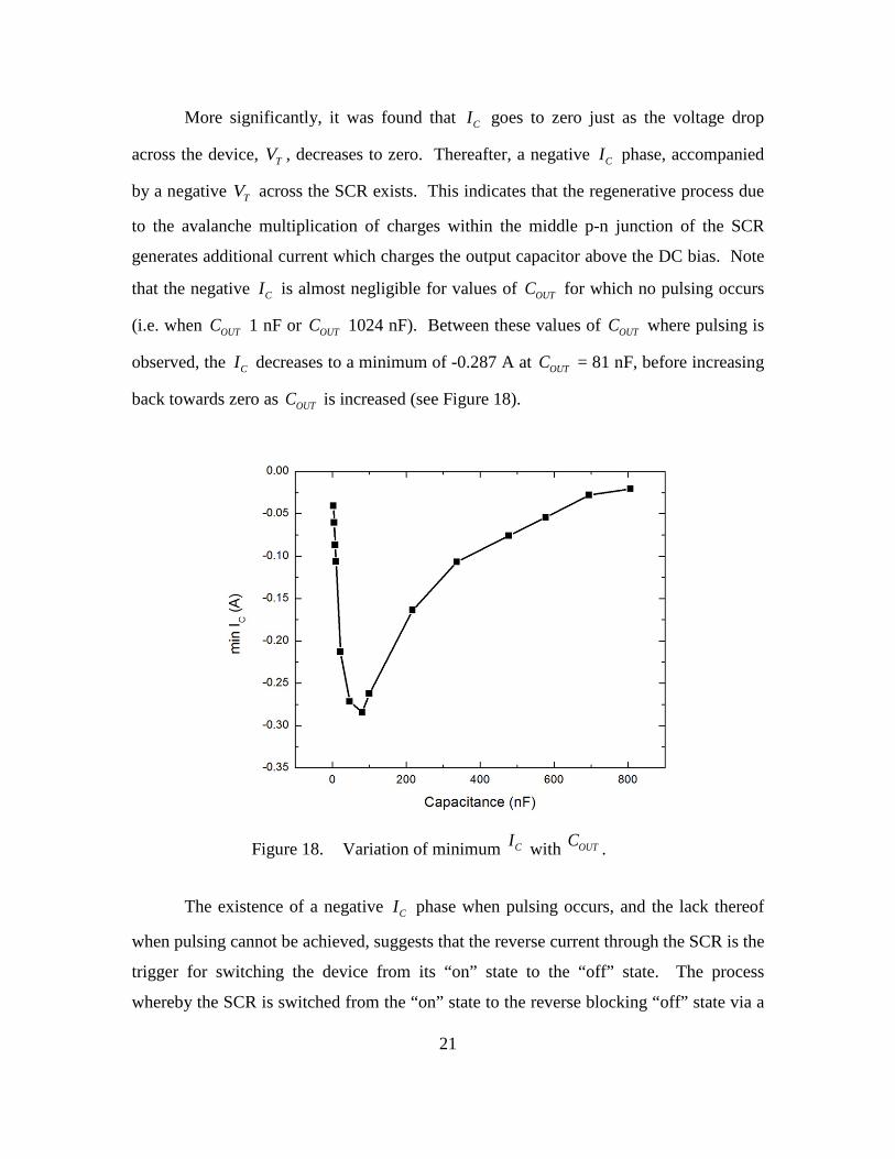
Figure 11. Measured I-V characteristic of MBS 4993 SCR. SI and SV are 0.044 mA and 8.96 V, respectively, while HI and HV are 0.223 mA and 0.562 V, respectively. .....................................................................................................12
Figure 12. Schematic of pulse generating circuit showing the DC power supply along with a capacitor bank to keep the DCV constant during the SCR switching. ...13
Figure 13. Picture of pulse generating circuit with MBS 4993 (SCR) connected in series with a parallel RC load...........................................................................13
Figure 14. Measured DCV , CI and TV during switching of SCR. A ringing was observed in the DCV transient response. This data is for a circuit with R = 47 kΩ and OUTC = 217 nF. ................................................................................15
ix

Figure 15. Rise time of RCV pulses saturates beyond capacitor banks larger than 121000 µF. .......................................................................................................16
Figure 16. Breakdown of switching process of the SCR. CI begins to increase while
TV drops as the device turns on. This data is for a circuit with R = 47 kΩ and OUTC = 100 nF. ...........................................................................................20
Figure 17. Measured variation of CI with OUTC . Magnitude of reverse current decreases as OUTC approaches the limits of pulsing.........................................20
Figure 18. Variation of minimum CI with OUTC ...............................................................21 Figure 19. Dependence of TV with time during switching for a set of OUTC values.
Magnified view of dependence of TV with OUTC is illustrated in Figure 20. ..23
Figure 20. Magnified view of dependence of TV with OUTC . It can be seen that for output capacitors of 1 nF and 1024 nF where pulsing is not achieved, TV does not fall below HV during most of reverse recovery period. .....................23
Figure 21. Dependence of TV with time for a selected set of OUTC . For output capacitors of 1 nF and 1024 nF where pulsing is not achieved, TV does not fall below HV even after the SCR’s turn-off time of 30 µs. ............................24
Figure 22. Variation of RI .with OUTC . RI does not increase beyond HI for OUTC = 1 nF or 1024 nF. ..................................................................................................25
Figure 23. Variation of TV with OUTC , just after SCR is switched on. The pulsing of the circuit requires TV to be below HV . ..........................................................26
Figure 24. Variation of ( )loge TV with time for a set of output capacitor values. Linear dependence observed for values of ( )loge TV between 0 and 1.5. .......27
Figure 25. Variation of SCRR with output capacitance, OUTC . ...........................................28
Figure 26. Measured TV during the switching of SCR for a set of values of R , OUTC maintained at 100 nF. .......................................................................................29
Figure 27. Variation of SCRI with R , OUTC .maintained at 100nF. ....................................30
Figure 28. Comparison of variation of TV with OUTC , just after SCR is switched on, and when different load resistors are used. For pulsing to be sustained, the upper limit of output capacitors is not dependent on the value of the load resistor. .............................................................................................................31
Figure 29. Change in load-line as resistor changes. Pulsing is still achieved for resistor values whose load-lines do not satisfy the static load-line criteria for pulsing. .......................................................................................................32
Figure 30. Comparison of TV transient response for gated (via photodiode) and un-gated pulsing. ...................................................................................................34
x
Figure 31. Comparison of SCRI transient response for gated (via photodiode) and un-gated pulsing. ...................................................................................................34
Figure 32. I-V characteristics of photodiode in dark and illuminated conditions; the amount of gate current injected is about 5 µA. ................................................35
Figure 33. Dynamic I-V characteristic of the MBS 4993 for a set of OUTC with load resistance of 47 kΩ. .........................................................................................36
Figure 34. Dynamic I-V characteristic of the MBS 4993 for OUTC = 100 nF and R = 47 kΩ. ..............................................................................................................36
xi

THIS PAGE INTENTIONALLY LEFT BLANK
xii

LIST OF ACRONYMS AND ABBREVIATIONS
BANKC capacitor bank
OUTC output capacitor
AI anode current of thyristor
CI current through output capacitor
HI holding current of silicon controlled rectifier
RI current through resistor
SI switching current of silicon controlled rectifier
SCRI current through silicon controlled rectifier
SCR silicon controlled rectifier
SCS silicon controlled switch
OFFt turn-off time of silicon controlled rectifier
AKV anode voltage of thyristor with respect to cathode
DCV DC bias
HV holding voltage of silicon controlled rectifier
RCV voltage across resistor and output capacitor
SV switching voltage of silicon controlled rectifier
xiii

THIS PAGE INTENTIONALLY LEFT BLANK
xiv

ACKNOWLEDGMENTS
This thesis would not have been possible without my advisors, Professor Gamani
Karunasiri and Dr. Fabio Alves. Their patience, enthusiasm and willingness to teach
have been inspirational.
In addition, I would also like to take the opportunity to acknowledge the technical
support provided by Sam Barone, who was always ready and willing to lend a hand in my
experiments.
Finally, and most importantly, to my kids, Jonas and Callum, who are my
constant reminder of a life outside of work, and my darling wife, Mei Ling, without
whom my journey in NPS would not have been this meaningful
xv

THIS PAGE INTENTIONALLY LEFT BLANK
xvi

I. INTRODUCTION
A. BACKGROUND
The thyristor, as defined by the International Electrotechnical Commission, is
“any semiconductor whose bistable action depends upon p-n-p-n regenerative action” [1].
Of the many semiconductor devices that fall under the thyristor family, the silicon
controlled rectifier (SCR) and the silicon controlled switch (SCS) are perhaps the most
important and widely used. Notably, both devices are able to switch from a high
impedance state (forward blocking mode) to a low impedance (conduction mode) state,
depending on the external bias and the gate current applied [2]. This has resulted in their
traditional application in the fields of electrical power and industrial electronics,
particularly for power regulation and control, and the provision of excess and low voltage
protection and short circuit current protection [1].
B. THYRISTOR THEORY OF OPERATION
The thyristor is essentially a p-n-p-n semiconductor structure with the top p-
layer, device anode (A), acting as the hole emitter and the bottom n- layer, device cathode
(K), as the electron emitter. The behavior of the thyristor in a circuit containing a series
load resistor and DC bias will first be discussed before the physics of its operation is
described qualitatively.
The AI - AKV characteristics of a typical thyristor along with a set of load lines
corresponding to varying DC bias are shown in Figure 1, where AI is the anode current
and AKV is the anode voltage with respect to the cathode. As AKV is gradually increased
from zero, the current through the thyristor increases at a much slower rate and remains
low, as indicated by the operating points on the lower branch of the AI - AKV
characteristic. The thyristor remains in the “off” state during this period. When DC bias
( )DCV is increased to 3DCV , the load line intersects the AI - AKV at an unstable point. The
corresponding AKV is known as the switching voltage of the thyristor, SV , and increasing
1

DCV beyond 3DCV switches the thyristor from a high-voltage, low-current (“off”) state to a
low-voltage, high-current (“on”) state. In the “on” state, the thyristor is now operating on
the upper branch of the AI - AKV characteristic as illustrated in Figure 1(a). When the
device is in the “on” state, reducing AKV will cause the thyristor to continue operating
along the upper branch of the curve until AI falls below the holding current, HI as
indicated in Figure 1(b). The thyristor is now in the “off” state and will continue
operating on the lower branch of the AI - AKV characteristic until it is switched on again
when DCV is increased beyond SV [3]–[5].
Figure 1. The p-n-p-n four layer diode in operation (after [3]). (a) Device is
switching to its “on” state. (b) Device is switching to its “off” state.
The thyristor’s switching phenomenon can be explained qualitatively through the
use of energy band diagrams [3]. For a positive bias applied across the device, there exist
two forward-biased p-n junctions and one reversed-biased junction, as seen in Figure 2a.
The positive bias causes holes injected from the 1p region to accumulate in the 2p
region because of the relatively narrower width of the 1n region. This accumulation of
holes in the 2p region results in an overall decrease in the potential energy which causes
the 2p region to move down on the energy band diagram as seen in Figure 2(b).
Consequently, this lowers the barrier at the reversed-biased 1n - 2p junction which in turn
2

enables more electrons to be injected from the 2n region into the 2p region. These
electrons subsequently accumulate in the 1n region, due to the narrow 2p layer, which
eventually increases the potential energy in the 1n region and moves it up on the energy
band diagram. This regenerative process is limited by the recombination current at the
forward-biased junctions, and for positive bias below SV , the overall current is limited to
a small value. However, as the bias is increased beyond SV , all the junctions in the
device are forward-biased, and large currents (limited to the loads in the circuit) are
conducted across the device. This is illustrated in Figure 2b.
Figure 2. The energy band of the p-n-p-n device (from [3]). (a) Under
positive DC bias, injected electrons accumulate in the 1n region and injected holes accumulate in the 2p region, thereby lowering the barrier at the reverse-biased junction. (b) Reverse-biased center
junction has been triggered into a forward-biased junction.
In the case of an SCR, an additional gate is connected at the 2p region as shown
in Figure 3. This enables one to apply suitable current pulses at the gate and achieve the
switching phenomena at significantly lower values of SV . For example, a positive
3

current pulse applied at the gate injects holes to the 2p region, thus making it more
positive and therefore lowers it on the energy band diagram. This in turn reduces the
barrier at the reversed-biased 1n - 2p junction and kick-starts the regenerative process
previously described (see Figure 4). Intuitively, the application of a positive current at
the gate would mean that less injection current is required at the device’s anode, and
therefore lower values of SV can be achieved.
Figure 3. Schematic diagram of the SCR (from [3]).
Figure 4. The energy band diagram of the SCR (from [3]). In this case,
switching of the SCR to its “on” state is via the application of a gate current.
4

C. RECENT DEVELOPMENTS
More recently, the possible exploitation of the SCR/SCS in other more novel
applications has been explored. It has been demonstrated that an SCR connected in series
with a parallel RC circuit under DC bias, as shown in Figure 5, was able to generate self-
terminating voltage pulses spontaneously, with the pulse rate increasing as the DC bias
was increased and saturating as the pulse period approached the RC time constant of the
circuit (see Figure 6). When a photodiode was connected to the gate terminal of the SCR,
the pulse rate was observed to increase with light intensity, as shown in Figure 7. This
lends credence to the possibility of adapting the SCR-based circuit as a pulse mode light
detector [6]. The use of such a simple circuit could potentially be extended to
applications that require the generation of voltage or current pulses in response to DC
stimulations, for example, in pulse mode optical sensing for the detection of light
sources [7] and in neural stimulators for retinal implants [8].
Figure 5. Schematic diagram of a pulse-generating circuit using an SCR
connected in series with a parallel RC ( R = 33 kΩ and C = 22 nF) load under DC bias (from [6]).
5
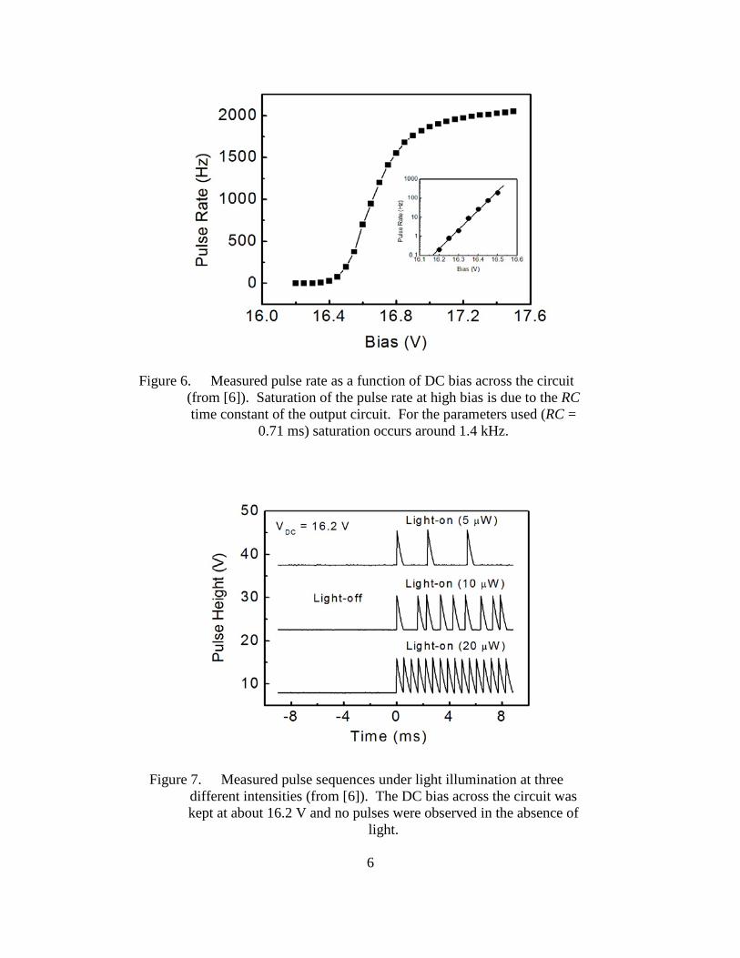
Figure 6. Measured pulse rate as a function of DC bias across the circuit
(from [6]). Saturation of the pulse rate at high bias is due to the RC time constant of the output circuit. For the parameters used (RC =
0.71 ms) saturation occurs around 1.4 kHz.
Figure 7. Measured pulse sequences under light illumination at three
different intensities (from [6]). The DC bias across the circuit was kept at about 16.2 V and no pulses were observed in the absence of
light.
6

The work performed on the use of the SCR-based circuit as a pulse mode light
detector was also extended to the field of radiation detection. Notably, a SCS-based
detector circuit was demonstrated to be able to detect ionizing radiation successfully [2].
As per the pulse mode light detector configuration, an SCS connected in parallel to an RC
load was able to generate large voltage pulses in response to the ionization events when
exposed to alpha particle radiation from an Am-241 source and beta particle radiation
from a Cs-137 source impinging on the reverse-biased middle p-n junction of the SCS, as
shown in Figure 8.
Figure 8. Compilation of the rate of detected emissions per minute (solid
squares) of a source of Cs-137, measured using a silicon p-i-n photodetector connected to the gate of the SCS as shown in the inset (from [2]). The solid line is a Gaussian fit with the average detection
rate of 15 per minute.
The advantages of using solid state radiation detectors [9], [10] are three-fold.
Firstly, the use of solids as a detecting medium, which are about 1000 times denser than
the gases used in gas ionization chambers, ensures that the resultant size of the
semiconductor detector is significantly less bulky since much smaller volumes are
required for capturing and detecting the radiation. Secondly, the ionization energy
required to generate a detection signal in semiconductor detectors is about an order of
magnitude lower than that of gas detectors, and this consequently improves the energy
7

resolution in the former significantly. In the case of a scintillator, while the fundamental
ionization energy required is comparable to that of a semiconductor detector, the
inefficient processes involved in the conversion of the ionization events into light pulses
and the subsequent conversion of photons into photoelectrons in the photomultiplier,
adversely impact the energy resolution available [11]. Thirdly, the SCS-based detector is
modeled as an electronic equivalent to a spark chamber [12], [13]. By biasing it near to a
trigger point, the SCS-based detector is able to return a large signal pulse with little or no
additional amplification circuitry. This is in stark contrast to a typical semiconductor
radiation detector, where additional circuitry, such as low-noise/high-gain amplifiers, is
essential to recover the relatively small current typically generated by the ionizing
radiation.
D. IMPETUS FOR THESIS
It was proposed that the SCS-based radiation detector is potentially able to
combine the advantages of the small size and low power consumption of semiconductor
detectors with the high gain and sensitivity of the gas detectors [2]. Notwithstanding,
work on the SCS-based detector is still in its nascent stages. One key concern is the dead
time between the voltage pulses returned, during which any radiation incident on the
detector will not be picked up. This is limited by the RC time constant of the circuit
used [2], and cannot be resolved by arbitrarily reducing the sizes of the resistive loads
and capacitance used in the circuit.
The inability to arbitrarily reduce the sizes of the resistive loads and capacitance
used is inherently due to the nature of the thyristor’s I-V characteristic. Notably, it was
proposed that for pulses to be sustained [6], the load line of the circuit has to intersect the
thyristor’s I-V characteristic at only one point between the device’s holding current, HI ,
and switching current, SI , or during the unstable transition regime of the device between
its “on” and “off” states, as shown in Figure 9. The equation of the load line is given in
(1).
DC T RV V I R= + (1)
8

where DCV is the DC bias, TV is the voltage across the SCR, RI is the current in the circuit and R is the series load resistor.
Figure 9. Static load-line switching criteria for thyristor. Load-line lies in
unstable transition regime of device between “on” and “off” states.
Intersection of the load line anywhere else on the I-V characteristic results in the
device remaining in either the “on” or “off” state and no pulsing is achieved. This
constraint on the placement of the load line means that the size of the resistor, R , must be
small enough to maintain the steady current above SI for turning the device on, and yet
large enough to keep the current below HI for switching the device off (i.e. the operating
point should be an unstable point along the unstable regime of the device’s I-V
characteristic). In addition, if the transition regime in the I-V characteristic of the device
is flatter or less inclined, larger resistor values, and consequently larger DC biases, would
be required for pulsing. Conversely, a more inclined transition regime in the I-V
characteristic would allow smaller resistor values to be chosen.
The objective of this thesis is therefore to re-examine the SCR-based pulse
generating circuit developed in [6], and determine how changes to the RC parameters of
the circuit impact its pulse generating capabilities, with the aim of improving the
sensitivity and speed of operation of the SCS-based radiation detector.
9

E. THESIS ORGANIZATION
This thesis is organized in the following manner:
Chapter II describes in detail how the SCS-based circuit was used to study the
intrinsic switching characteristic of the thyristor. Emphasis is placed on how the DC bias
was regulated, how the IV characteristics of the thyristor were determined, and how the
values of the resistance and the capacitance in the load circuit were varied to observe
their impact on the voltage and current pulses generated.
Chapter III presents and analyzes the observations made on the pulse-generating
capability of the circuit when resistance and capacitance were varied. Significantly, key
observations underpinning the switching mechanism of the device are discussed here,
along with the development of the dynamic I-V characteristics of the thyristor.
Chapter IV concludes the thesis and provides recommendations for future
research work.
10

II. EXPERIMENTAL SETUP
A. PULSE GENERATING CIRCUIT
The MBS 4993 silicon bidirectional switch was the SCR of choice due to its low
voltage switching characteristics (low SV of 8 V typically). The I-V characteristic of this
device was determined using the circuit shown in Figure 10. The DC bias was steadily
increased from 0 V and values of DCV and RV recorded. The potential difference across
the device ( )T DC RV V V= − was plotted against the current through it ( )/R RI V R= to give
the I-V characteristic in Figure 11.
Figure 10. Schematic of circuit used to determine I-V characteristic of MBS
4993 SCR.
11
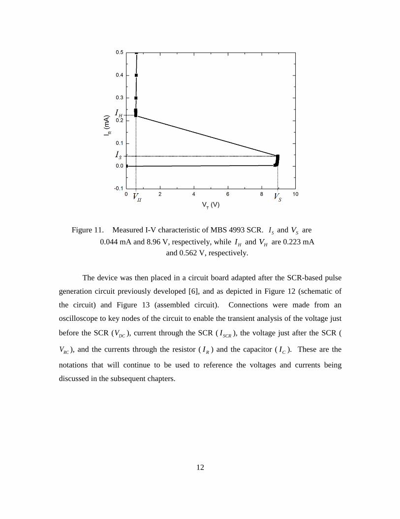
Figure 11. Measured I-V characteristic of MBS 4993 SCR. SI and SV are
0.044 mA and 8.96 V, respectively, while HI and HV are 0.223 mA and 0.562 V, respectively.
The device was then placed in a circuit board adapted after the SCR-based pulse
generation circuit previously developed [6], and as depicted in Figure 12 (schematic of
the circuit) and Figure 13 (assembled circuit). Connections were made from an
oscilloscope to key nodes of the circuit to enable the transient analysis of the voltage just
before the SCR ( DCV ), current through the SCR ( SCRI ), the voltage just after the SCR (
RCV ), and the currents through the resistor ( RI ) and the capacitor ( CI ). These are the
notations that will continue to be used to reference the voltages and currents being
discussed in the subsequent chapters.
12

Figure 12. Schematic of pulse generating circuit showing the DC power
supply along with a capacitor bank to keep the DCV constant during the SCR switching.
Figure 13. Picture of pulse generating circuit with MBS 4993 (SCR)
connected in series with a parallel RC load.
13

B. SELECTION OF RESISTORS
As previously discussed, the size of the resistor to be used has to be small enough
to maintain the steady current above SI for turning the device on, and yet large enough to
keep the current below HI for switching the device off. This is summarized by the
following relations:
For the SCR to switch on,
DC S
R S SV VI I I
R−
≥ ⇒ ≥ (2)
For the SCR to switch off,
DC H
R H HV VI I I
R−
≤ ⇒ ≤ (3)
For a desired DC bias of approximately 11 V, an initial resistor value of 47 kΩ
was chosen to initialize the pulsing.
C. INCORPORATION OF CAPACITOR BANK
In the early stages of the experiment, oscillations or ringing were observed at the
DCV node of the circuit during the switching process although the value should remain
constant (see Figure 14). As the potential difference across the SCR, TV , was increased
beyond SV , the SCR switched from a high impedance state to a low impedance state,
resulting in a sudden surge in the current through the circuit. It was hypothesized that the
oscillations observed in the transient response of DCV was due to the inability of the
power supply to meet the surge in current during the switching process. Note that nearly
all the transient current during switching passes through the output capacitor due to its
smaller impedance as compared to the load resistor.
14

Figure 14. Measured DCV , CI and TV during switching of SCR. A ringing
was observed in the DCV transient response. This data is for a circuit with R = 47 kΩ and OUTC = 217 nF.
To test this hypothesis, a capacitor bank was connected in parallel to the voltage
source as previously depicted in Figure 12, while a 47 kΩ resistor and a 217 nF capacitor
were connected in parallel to the SCR to initiate pulsing. It was proposed that an
adequately sized capacitor bank would possess the necessary amount of stored charges
required by the surge in current during the SCR’s switching process, thus curtailing the
emergence of oscillations in the DCV response. To determine the size of the capacitor
bank required, capacitors were added to the bank in increments of 22 µF or 33 µF, and
the rise time of the RCV pulses measured for each incremental step. The rise time of the
RCV pulses, as a function of the size of the capacitor bank, was found to saturate for
values of capacitance beyond 121000 µF, as shown in Figure 15, which suggested that
capacitor banks larger than this would possess sufficient stored charge to meet the
demands of the SCR’s switching process. A 165000 µF capacitor bank was then
included in the circuit.
15

Figure 15. Rise time of RCV pulses saturates beyond capacitor banks larger
than 121000 µF.
Notwithstanding, ringing continued to be observed even after the inclusion of the
165000 µF capacitor bank, with a significant pull-down of 0.9 V in the DCV transient
response during the switching process. An analysis of the charge transfer from the
capacitor bank to the output capacitor during the switching process was then performed
in an attempt to understand this behavior.
The reduction of charge in the capacitor bank due to the pull-down in the DC
level, DCV∆ , can be estimated using
DC BANKQ V C∆ = ∆
(4)
The amount of charge stored by capacitor, OUTC , during switching can be
estimated using the measured current CI :
OUT RC
CC VQI
t t∆
= =∆ ∆ (5)
16

If the reduction of charge on the capacitor bank is used for charging the output
capacitor, the pull down in DC level is given by:
OUT RC DC BANKC V V C= ∆
(6)
OUT RC
DCBANK
C VVC
∆ = (7)
Using (7), the pull-down in the DCV voltage was found to be approximately 14
µV, for a capacitor bank, BANKC , of 165000 µF and OUTC of 217 nF. This was
significantly smaller and contrary to the actual pull-down observed, which suggests that
the ringing observed on the oscilloscope was not due to the sudden demand of charges
during pulsing since the capacitor bank was theoretically able to stabilize the DCV
transient response. It was concluded that the ringing was therefore caused by the
inductive loading of the probe connected to the oscilloscope during pulsing. The fast rise
time ( < 1 µs), coupled with the surge in current accompanying each pulse indicate that
the rate of change of current with time, dIdt
, was large ( 1A/ µs). This was likely to
have induced a back emf, which presented itself as the large pull-down in the DCV
transient response observed during pulsing. For the thesis work that followed, the
165000 µF capacitor bank was included in the circuit, with the ringing in the DCV
transient response ignored.
Measurements of the transient responses of voltages and currents at the key nodes
of the circuit were measured as OUTC was varied from 1 nF to 1024 nF for a fixed load
resistor of 47 kΩ, and again as R was varied from 800 Ω to 50 kΩ for a selected value of
OUTC . These were analyzed to determine the effect both OUTC and R had on the pulse
generating capability of the circuit.
17

THIS PAGE INTENTIONALLY LEFT BLANK
18

III. RESULTS AND ANALYSIS
A. REVERSE CURRENT OBSERVATIONS DURING SWITCHING
The transient analysis of CI with variations in OUTC (between 1 nF to 1024 nF)
provided useful insights into the switching characteristic of the circuit. Figure 16 shows
a typical switching characteristic of the SCR. When the SCR begins to switch from its
“off” state to its “on” state, CI increases from SI to a maximum value before falling back
to very a small value again. In addition, the increase in OUTC increases the maximum
value of CI , and also lengthens the duration of the positive current surge as shown in
Figure 17. This is expected because the larger OUTC will undoubtedly draw more charges
across the SCR when the latter is turned on, while the longer period of positive current
surge is determined by the SCR OUTR C time constant of the circuit, where SCRR is the
resistance of the SCR. The amount of charge in COUT is estimated by integrating the
positive CI and the result is observed to agree closely to that obtained using (5). This
substantiates the assumption that the duration of the positive current surge corresponds to
the period when the SCR is in the “on” state and that all the current passed through the
device goes towards charging OUTC .
19

Figure 16. Breakdown of switching process of the SCR. CI begins to
increase while TV drops as the device turns on. This data is for a circuit with R = 47 kΩ and OUTC = 100 nF.
Figure 17. Measured variation of CI with OUTC . Magnitude of reverse current
decreases as OUTC approaches the limits of pulsing. 20
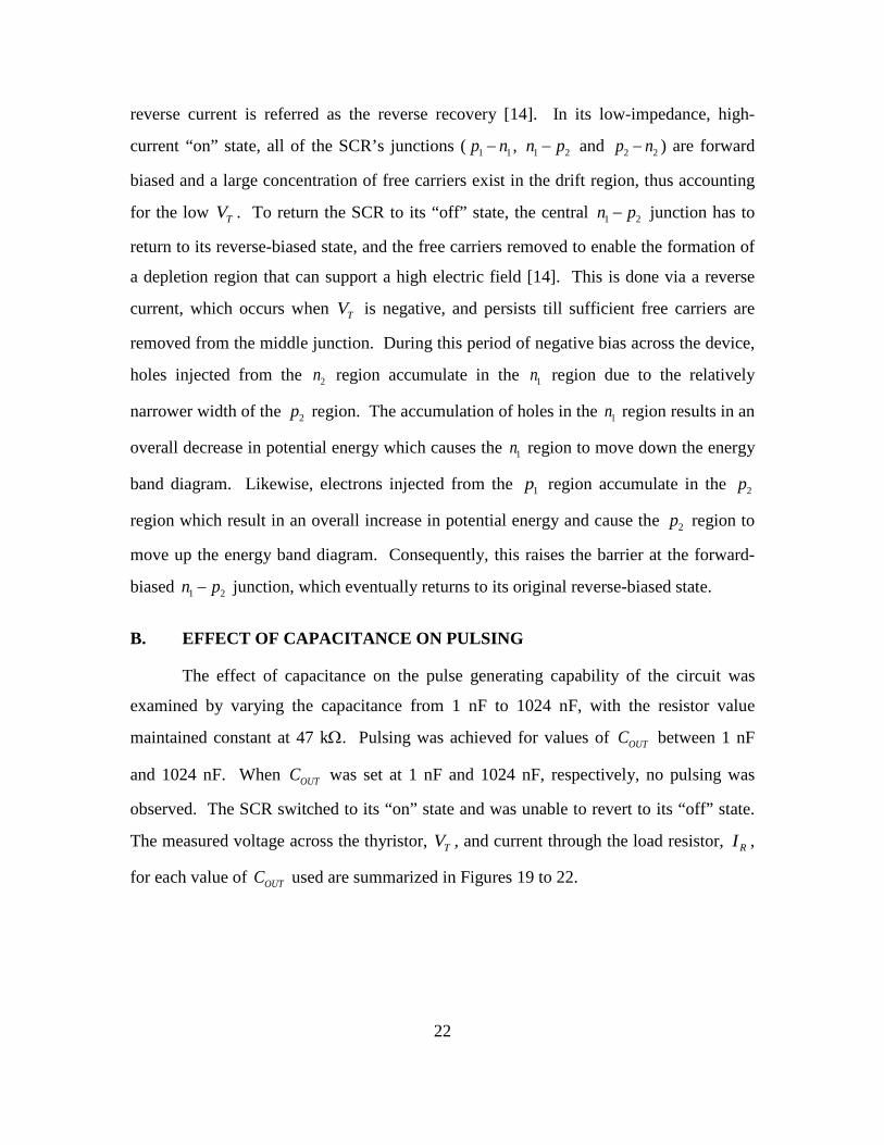
More significantly, it was found that CI goes to zero just as the voltage drop
across the device, TV , decreases to zero. Thereafter, a negative CI phase, accompanied
by a negative TV across the SCR exists. This indicates that the regenerative process due
to the avalanche multiplication of charges within the middle p-n junction of the SCR
generates additional current which charges the output capacitor above the DC bias. Note
that the negative CI is almost negligible for values of OUTC for which no pulsing occurs
(i.e. when OUTC 1 nF or OUTC 1024 nF). Between these values of OUTC where pulsing is
observed, the CI decreases to a minimum of -0.287 A at OUTC = 81 nF, before increasing
back towards zero as OUTC is increased (see Figure 18).
Figure 18. Variation of minimum CI with OUTC .
The existence of a negative CI phase when pulsing occurs, and the lack thereof
when pulsing cannot be achieved, suggests that the reverse current through the SCR is the
trigger for switching the device from its “on” state to the “off” state. The process
whereby the SCR is switched from the “on” state to the reverse blocking “off” state via a
21
reverse current is referred as the reverse recovery [14]. In its low-impedance, high-
current “on” state, all of the SCR’s junctions ( 1 1p n− , 1 2n p− and 2 2p n− ) are forward
biased and a large concentration of free carriers exist in the drift region, thus accounting
for the low TV . To return the SCR to its “off” state, the central 1 2n p− junction has to
return to its reverse-biased state, and the free carriers removed to enable the formation of
a depletion region that can support a high electric field [14]. This is done via a reverse
current, which occurs when TV is negative, and persists till sufficient free carriers are
removed from the middle junction. During this period of negative bias across the device,
holes injected from the 2n region accumulate in the 1n region due to the relatively
narrower width of the 2p region. The accumulation of holes in the 1n region results in an
overall decrease in potential energy which causes the 1n region to move down the energy
band diagram. Likewise, electrons injected from the 1p region accumulate in the 2p
region which result in an overall increase in potential energy and cause the 2p region to
move up the energy band diagram. Consequently, this raises the barrier at the forward-
biased 1 2n p− junction, which eventually returns to its original reverse-biased state.
B. EFFECT OF CAPACITANCE ON PULSING
The effect of capacitance on the pulse generating capability of the circuit was
examined by varying the capacitance from 1 nF to 1024 nF, with the resistor value
maintained constant at 47 kΩ. Pulsing was achieved for values of OUTC between 1 nF
and 1024 nF. When OUTC was set at 1 nF and 1024 nF, respectively, no pulsing was
observed. The SCR switched to its “on” state and was unable to revert to its “off” state.
The measured voltage across the thyristor, TV , and current through the load resistor, RI ,
for each value of OUTC used are summarized in Figures 19 to 22.
22

Figure 19. Dependence of TV with time during switching for a set of OUTC
values. Magnified view of dependence of TV with OUTC is illustrated in Figure 20.
Figure 20. Magnified view of dependence of TV with OUTC . It can be seen
that for output capacitors of 1 nF and 1024 nF where pulsing is not achieved, TV does not fall below HV during most of reverse recovery
period. 23

Figure 21. Dependence of TV with time for a selected set of OUTC . For output
capacitors of 1 nF and 1024 nF where pulsing is not achieved, TV does not fall below HV even after the SCR’s turn-off time of 30 µs.
Two stark observations are immediately apparent from Figures 19 and 20. Firstly,
it can be seen that for all values of OUTC , TV first decreases rapidly from 8.9 V to a
minimum value when switching occurs, then increases fairly rapidly to a transient peak
before flattening out and thereafter returning to its pre-pulsed value of 8.9V at the end of
each pulse (not shown due to long duration of time). Secondly, for OUTC of 1 nF and
1024 nF where pulsing is not achieved, the values at which TV plateaus are above the
SCR’s holding voltage ( HV = 0.562V). This observation holds true even after the SCR’s
specified turn-off time, OFFt , of 30 µs, as shown in Figure 21. As OUTC is increased from
1 nF, the value at which TV plateaus is observed to decrease to a minimum of -0.18V at
217 nF before increasing steadily again. In addition, at the initial stage of discharging of
OUTC , RI does not increase beyond the SCR’s holding current ( HI =2.23 mA) for OUTC
of 1 nF and 1024 nF (where no pulsing was observed) as shown in Figure 22.
24

Figure 22. Variation of RI .with OUTC . RI does not increase beyond HI for OUTC = 1 nF or 1024 nF.
The SCR’s ability to switch from its “on” state to its “off” state is dependent on
TV falling below HV , and RI increasing beyond HI . The lack of pulsing observed for
OUTC of 1 nF and 1024 nF is therefore due to TV and RI failing to meet these criteria. In
addition, the manner in which TV varies with OUTC , as shown in Figure 23, suggests that
there exists a range of values of OUTC for which pulsing is most favorable (i.e where TV
is much smaller than HV ).
25

Figure 23. Variation of TV with OUTC , just after SCR is switched on. The
pulsing of the circuit requires TV to be below HV .
The lack of pulsing achieved at the extreme ends of OUTC can further be explained
by the RC time constants involved in the charging and discharging of OUTC during each
pulse. When the SCR is switched to its “on” state, outC is being charged and its rate of
charging is governed by the SCR OUTR C time constant, where SCRR is the dynamic
resistance of the SCR when it is conducting, which is typically a few ohms. When OUTC
is fully charged, TV across the SCR is at its minimum and the SCR commences switching
back to its “off” state. During this period, OUTC discharges through R and this discharge
rate is governed by the OUTRC time constant. For a high OUTC of 1024 nF, pulsing does
not occur because the time it takes for the large capacitor to fully charge is substantially
longer than the turn-off time of the SCR, OFFt , as summarized in (8).
SCR OUT OFFR C t>
(8)
26

Thus, the voltage across the SCR, TV , does not fall below the device’s holding
voltage, HV , within the device’s turn-off time. The device remains in the “on” state
without being able to revert to its “off” state, and no pulsing occurs. In order to
determine the upper limit of OUTC , SCRR was estimated using the data in Figure 19. The
plots of ( )loge TV with time, for a set of output capacitor values, show linear dependence
as illustrated in Figure 24 due to the charging of OUTC via the “on” state resistance of the
SCR. The dynamic resistance of the SCR varies from 36.7 Ω to 1.4 Ω as the size of the
output capacitor is varied from 1 nF to 1024 nF (see Figure 25). In addition, the turn-off
time of the SCR used (MBS4993) as specified in the data sheet is about 30 µs [15]. This
gives the upper limit of the output capacitor needed as 20 µF, which agrees fairly well
with the experimental observations.
Figure 24. Variation of ( )loge TV with time for a set of output capacitor
values. Linear dependence observed for values of ( )loge TV between 0 and 1.5.
27

Figure 25. Variation of SCRR with output capacitance, OUTC .
On the other hand, pulsing does not occur for small values of OUTC because the
time taken for the capacitor to begin discharging is much shorter than the turn-off time of
the SCR. Thus, the voltage across the output capacitor starts decreasing relatively fast,
thereby pushing the voltage across the SCR above the holding voltage within the turn-off
time of the device. This is summarized in (9).
out OFFRC t<
(9)
Based on the 30 µs turn-off time of the SCR and a load resistance of 47 kΩ, the
minimum output capacitance needed is about 0.6 nF, which is in good agreement with the
experimental value of above 1 nF required for pulsing. Leveraging the reverse current
analysis previously discussed, the short discharge time of the smaller-sized OUTC suggests
that the reverse current from OUTC may not only be insufficient to remove the free
carriers in the device, and return the 1 2n p− junction to its reverse-biased state, but also
lacking in the time available for the process to be reversed. This explains why the SCR
could only be switched on but not turned off for small values of the output capacitor.
28

C. EFFECT OF RESISTANCE ON PULSING
The effect of the load resistance on the pulse generating capability of the circuit
was also examined by varying the resistor values from 800 Ω to 50 kΩ, with OUTC
maintained constant at 100 nF. The transient measurements of voltage across the SCR,
TV , and current through it, SCRI , for the set of resistor values used are summarized in
Figure 26 and Figure 27, respectively.
Figure 26. Measured TV during the switching of SCR for a set of values of R ,
OUTC maintained at 100 nF.
29

Figure 27. Variation of SCRI with R , OUTC .maintained at 100nF.
It can be seen in Figure 27 that changing the resistor values had no impact on SCRI . This is to be expected since OUTC , which is responsible for the transient current
through the SCR when the device switches to its “on” state, is fixed in this case. The
effect of varying the load resistance is apparent only when the SCR is reverting to its
“off” state, as seen in Figure 26, where the rate of increase of TV increases with
decreasing R . This lends further credence to the previous discussion which indicated
that the ability of the device to switch off should satisfy out OFFRC t> . Thus, a smaller load
resistor requires a larger output capacitor to sustain pulsing and this agrees well with the
measured range of OUTC for which pulsing occurred when different load resistors were
used (see Figure 28). Specifically, pulsing was achieved only for OUTC values between
81 nF and 1024 nF when the 800 Ω load resistor was used. This lower limit of OUTC was
significantly higher as compared to a 47 kΩ resistor circuit. From (9), using a lower R
of 800 Ω means that a larger OUTC is required for OUT OFFRC t> to be satisfied for pulsing
to ensue. This ensures that the time required by the SCR to revert to its “off” state is not
restricted by the discharge time of OUTC . In addition, the upper limit of the output 30

capacitance required to sustain pulsing is not affected by the value of the load resistor
used since it only depends on the on-resistance of SCR.
Figure 28. Comparison of variation of TV with OUTC , just after SCR is
switched on, and when different load resistors are used. For pulsing to be sustained, the upper limit of output capacitors is not dependent
on the value of the load resistor.
To note, pulsing was achieved for resistor values as low as 800 Ω although these
values do not satisfy the static load-line criteria set forth previously and as illustrated in
Figure 29. This is because the static load-line analysis previously described was
applicable for a circuit with only a resistive load. With the RC load in our case, the
current generated during the switching primarily passes through the output capacitor due
to its low impedance and at fast switching speeds. When pulsing occurs, the dynamics of
the circuit become more convoluted, and (1) should be modified to account for the
impedance of OUTC as given in (10). However, analyzing the dynamic circuit equation to
explain this phenomenon is complex since the angular frequency, ω , is not a constant.
1DC T R
OUT
V V I Rj Cω
= + +
(10)
31

Figure 29 shows a set of load lines with varying load resistances. It can be seen
that only R = 50 kΩ has a single unstable operating point that lies between SI and HI of
the SCR’s I-V characteristics. This instability would enable the SCR to be triggered
between its “on” and “off” states, as previously explained. On the other hand, the other
resistors each possess two stable operating points on the I-V characteristics: one below SI
and the other above HI . In theory, no pulsing should occur for these resistors and the
SCR should simply switch from its “off” state to its “on” state and remain there. The fact
that pulsing occurs can be attributed to the role that the output capacitor, OUTC , plays
during the switching process. It can be seen from Figure 26 that switching occurs within
about 1 µs, which is close to the SCR’s turn-on time of 1 µs. This suggests the
possibility that OUTC was able to charge up and establish a negative bias across the SCR
before the device could turn on fully and reach its stable operating point above HI . The
negative bias, TV , then drove a reverse current, SCRI , through the SCR and returned the
device to its “off” state, thus allowing pulsation.
Figure 29. Change in load-line as resistor changes. Pulsing is still achieved
for resistor values whose load-lines do not satisfy the static load-line criteria for pulsing.
32

D. EFFECT OF GATE CURRENT ON PULSING
In order for the circuit to be incorporated into light detection or ionizing radiation
detection applications, it is important to understand the effect of triggering the SCR
externally for pulse generation. The SCR can be triggered either by sending a current
through the gate terminal or by shining light or radiation on the middle p-n junction. For
the purposes of this thesis, the provision of a gate current was conveniently achieved by
connecting a photodiode to the gate of the SCR in the reverse-biased configuration. DC
bias was increased till the onset of pulsing and TV and SCRI were measured for OUTC = 3
nF and R = 47 kΩ. These were compared against the TV and SCRI transient responses
for an un-gated, DC bias-triggered pulsing of the SCR, as shown in Figure 30 and Figure
31, respectively. The I-V characteristics of the photodiode with and without illumination
were also measured using a parameter analyzer and illustrated in Figure 32. A 5 µA
photocurrent was generated when the photodiode was illuminated based on the data in
Figure 32.
As expected, the injection of a gate current enabled pulsing to be sustained at a
lower DC bias. In addition, the gated and un-gated transient SCRI responses were
comparable in profile with slight differences in their magnitude. This suggests that the
switching mechanism of the SCR is not sensitive to the means by which it is triggered, be
it an un-gated, DC bias or via a gate current. The higher SCRI with gated triggering is
possibly due to an increase of avalanche generation with additional holes injected into the
2p layer via the gate terminal.
33

Figure 30. Comparison of TV transient response for gated (via photodiode)
and un-gated pulsing.
Figure 31. Comparison of SCRI transient response for gated (via photodiode)
and un-gated pulsing.
34

Figure 32. I-V characteristics of photodiode in dark and illuminated
conditions; the amount of gate current injected is about 5 µA.
E. DYNAMIC I-V CHARACTERISTICS OF MBS 4993
As previously mentioned, a static load-line analysis of the circuit is not applicable
when pulsing occurs with a RC load. The I-V characteristic of the SCR during pulsing is
needed for describing the dynamics of the circuit. This is done by using the transient data
SCRI and TV for a given OUTC , and plotting SCRI vs TV as shown in Figure 33.
At a first glance, the dynamic I-V characteristic of the SCR differs significantly
from its static I-V profile. Notably, the amplitudes of the currents involved during
pulsing (-0.26 A – 2.86 A) are approximately three orders of magnitude larger than in the
static case (0 mA – 0.25mA). Secondly, the large differences in the I-V characteristic
when OUTC is varied clearly emphasize the significant role OUTC plays in the generation
of pulses. Thirdly, the impedance of the device is obviously not a constant as evidenced
by the non-linear behavior of TV with SCRI .
35

Figure 33. Dynamic I-V characteristic of the MBS 4993 for a set of OUTC with
load resistance of 47 kΩ.
Figure 34. Dynamic I-V characteristic of the MBS 4993 for OUTC = 100 nF
and R = 47 kΩ.
36

The dynamic I-V characteristic of the SCR is examined in closer detail using the
data for OUTC = 100 nF (see Figure 34). As the plot is created using the time-dependent
response of both TV with SCRI , the I-V characteristic is intrinsically a function of time as
well. When pulsing first occurs at point A, TV across the SCR drops from SV as the
device switches to its “on” state. The forward-biasing of all of the SCR’s three junctions
( 1p - 1n , 1n - 2p and 2p - 2n ) due to avalanche multiplication of injected charges from the
outer two p-n junctions ( 1p - 1n and 2p - 2n ) into the middle 1n - 2p junction gives rise to a
surge in the current through the circuit. The upper branch of the I-V characteristic from
point A to point B illustrates this. During this period, OUTC is charged and from point B
to point C, TV decreases with SCRI as the charging of OUTC nears completion. At point C,
the charge on OUTC is at its maximum while TV across the SCR is close to zero. Between
points C and D, a reverse current exists to return the SCR to its “off” state. The
switching of the SCR to its “off” state is depicted by the lower branch of the I-V
characteristic from points D to A. When TV across the device increases beyond SV , the
switching process is repeated and a new pulse occurs.
37

THIS PAGE INTENTIONALLY LEFT BLANK
38

IV. CONCLUSION AND RECOMMENDATIONS
In this thesis, we have shown definitively that the SCR switches from its “on”
state to its “off” state via a reverse recovery current (negative SCRI ) that is accompanied
by a negative voltage drop across the device. This reverse recovery current is needed to
remove the free carriers in the drift region and return the central 1 2n p− junction to its
reverse-biased “off” state. In addition, the regenerative process by which charges are
avalanched into the circuit when the SCR is turned on appears to be independent of the
mode of triggering (i.e. via direct un-gated DC bias or using a current at the gate).
However, the magnitude of current generated during the switching depends on the gating
mechanism employed.
Significantly, in wanting to improve the sensitivity of the pulse generating circuit
for radiation detection, we also established that the extent to which the dead time between
the pulses (i.e. the OUTRC time constant of each pulse) can be reduced is in fact
constrained by the SCR’s intrinsic turn-off time, OFFt . This means that without making
modifications to the SCR itself, the minimum dead time achievable for pulsing to be
sustained is essentially the turn-off time of the SCR. Reducing R and/or OUTC such that
OUT OFFRC t< will not enable pulsing, as previously demonstrated and discussed.
To further increase the sensitivity of the circuit, future work may require
modifications to be made to the SCR itself. Typically, the SCR’s turn-off time can
possibly be lowered by doping the device with minority carrier lifetime killing impurities
such as gold. In addition, it was further proposed that confining the doping of the
minority carrier lifetime killing impurities to a thin region of the device in a plane
perpendicular to the on-state current flow would make for better reduction in turn-off
times [16]. Alternatively, the introduction of additional anode gates at the 1n layer could
be explored to reduce OFFt since positive turn-off time improvements of up to 55% could
apparently be achieved [17].
39

THIS PAGE INTENTIONALLY LEFT BLANK
40

LIST OF REFERENCES
[1] P. Atkinson, Thyristors and their Applications, 1st ed. London, United Kingdom: Mills and Boon Limited, 1972, pp. 9–11.
[2] F. Alves, C. Smith, and G. Karunasiri. (2014, Sep. 1). A solid-state spark chamber for detection of ionizing radiation. Sensors and Actuators A: Physical. [Online]. 216. pp. 102-105. Available: http://www.sciencedirect.com/science/article/pii/S0924424714002581
[3] B. L. Anderson and R.L. Anderson, Fundamentals of Semiconductor Devices, 1st
ed. New York: McGraw-Hill, 2005, pp. 650–657.
[4] S. M. Sze and K. K. Ng, Physics of Semiconductor Devices, 3rd ed. Hoboken, New Jersey: John Wiley and Sons, 2007, pp. 548-574.
[5] A. Blicher, Thyristor Physics, 1st ed. New York: Springer-Verlag, 1976, pp. 1–72.
[6] G. Karunasiri. (2006, July 10). Spontaneous pulse generation using silicon controlled rectifier. Applied Physics Letters. [Online]. 89(2), pp. 23501-1–23501-3. Available: http://scitation.aip.org/content/aip/journal/apl/89/2/10.1063/1.2220528
[7] G. de Graaf and R. F. Wolffenbuttel. (2004, Feb. 1). Optical CMOS sensor system for detection of light sources. Sensors and Actuators A: Physical. [Online]. 110(1), pp. 77–81. Available: http://www.sciencedirect.com/science/article/pii/S0924424703005843
[8] M. Mahadevappa, J. D. Weiland, D. Yanai, I. Fine, R. J. Greenberg, and M. S. Humayun. (2005, June 13). Perceptual thresholds and electrode impedance in three retinal prosthesis subjects. IEEE Transactions on Neural Systems and Rehabilitation Engineering. [Online]. 13(2), pp. 201-206. Available: http://ieeexplore.ieee.org/xpl/login.jsp?tp=&arnumber=1439546&url=http%3A%2F%2Fieeexplore.ieee.org%2Fxpls%2Fabs_all.jsp%3Farnumber%3D1439546
[9] H. Dijkstra and J. Libby. (2002, Nov. 21). Overview of silicon detectors. Nuclear Instruments and Methods in Physics Research A. [Online]. 494(1), pp. 86–93. Available: http://www.sciencedirect.com/science/article/pii/S016890020201450X
[10] D. Bortoletto. (2010, Mar. 19). Solid state detectors. Nuclear Instruments and Methods in Physics Research A. [Online]. 623(1), pp. 35–41. Available: http://www.sciencedirect.com/science/article/pii/S0168900210004146
41

[11] F. S. Goulding and Y. Stone. (1970, Oct. 16). Semiconductor radiation detectors. Science. [Online]. 170(3955), pp. 280–289. Available: http://www.sciencemag.org/content/170/3955/280.abstract
[12] C. Leroy. “Review of radiation detectors,” in American Institute of Physics Conference Proceedings 1204, 2010, vol. 49, pp. 49–57.
[13] P. Fonte. (2002, June 3). Applications and new developments in resistive plate chambers. IEEE Transactions on Nuclear Science. [Online]. 49(3), pp. 881–887. Available: http://ieeexplore.ieee.org/xpl/login.jsp?tp=&arnumber= 1039583&url=http%3A%2F%2Fieeexplore.ieee.org%2Fiel5%2F23%2F22285%2F01039583.pdf%3Farnumber%3D1039583
[14] B. J. Baliga, Fundamentals of Power Semiconductor Devices, 1st ed. New York: Springer Science, 2008, pp. 625–697.
[15] Semiconductor Technical Data for MBS 4991/4992/4993, Motorola, Phoenix, AZ, 1995, pp. 1–5.
[16] V. A. K. Temple and F. W. Holroyd. (1983, July). Optimizing carrier lifetime profile for improved trade-off between turn-off time and forward drop. IEEE Transactions on Electron Devices. [Online]. 30(7), pp. 782–790. Available: http://ieeexplore.ieee.org/xpl/articleDetails.jsp?arnumber=1483111&sortType%3Dasc_p_Sequence%26filter%3DAND%28p_IS_Number%3A31879%29
[17] H. B. Assalit and G. H. Studtmann. Description of a technique for the reduction of thyristor turn-off time. IEEE Transactions on Electron Devices. [Online]. 21(7), pp. 416-420. Available: http://ieeexplore.ieee.org/xpl/articleDetails.jsp?arnumber=1477757&sortType%3Dasc_p_Sequence%26filter%3DAND%28p_IS_Number%3A31726%29
42

INITIAL DISTRIBUTION LIST
1. Defense Technical Information Center Ft. Belvoir, Virginia 2. Dudley Knox Library Naval Postgraduate School Monterey, California
43