Embed Size (px)
Citation preview
Hindawi Publishing CorporationISRN NanomaterialsVolume 2013 Article ID 504341 7 pageshttpdxdoiorg1011552013504341
Research ArticleOptical Absorption in Nano-Structures Classical andQuantum Models
Anand Kulkarni Durdu Guney and Ankit Vora
Department of Electrical and Computer Engineering Michigan Technological University Houghton MI 49931 USA
Correspondence should be addressed to Durdu Guney dguneymtuedu
Received 11 September 2013 Accepted 7 October 2013
Academic Editors M R Ferreira and M Mirzaei
Copyright copy 2013 Anand Kulkarni et alThis is an open access article distributed under theCreativeCommonsAttribution Licensewhich permits unrestricted use distribution and reproduction in any medium provided the original work is properly cited
In the last decade nano-structured materials have gained a significant interest for applications in solar cells and other optical andopto-electronic devices Due to carrier confinement the absorption characteristics in these structures are quite different from theabsorption in bulk materials and thin films Optical absorption coefficients of a silicon nano-wire are obtained based on a semi-classical model where the photon-electron interaction is described by the interaction of an electromagnetic wave with the electronsin the valence band of a semiconductorThe absorption characteristics showed enhanced optical absorption but no resonant peaksIn our modified model we have identified optically active inter band transitions by performing electronic structure calculationson unit cells of nano-dimensions The absorption spectrum obtained here shows explicit excitonic processes This absorption istunable from the visible region to near UV portion of the solar spectrum In our previous work on thin films (100 nm) of ITO wehave used classical Drude model to describe free electron absorption Using the imaginary part of the calculated complex dielectricfunction we have plotted the absorption coefficient versus wavelength of the photon and compared with the experimental datashowing good agreement between theory and experiment
1 Introduction
The efficiency of a solar cell is dependent on the opticalabsorption of the material used to fabricate the solar cellIn bulk crystalline materials and even in thin films thebulk absorption coefficient is the most important parameterthat determines the optical absorption Classical modelssuch as Drude model or Drude-Lorentz model describe theoptical absorption based on the complex dielectric function[1 2] This approach works very well for the absorptionof photons by the electrons inside a band for exampleconduction band However from band to band excitationof electrons a detailed understanding of the band structureof the material is essential To calculate band structure insemiconductors one has to invoke quantum mechanicalmodels using Schrodingerrsquos wave equation [3 4] In thispaper we illustrate the applications of classical and quantummodels with examples from our past research on indiumtin oxide (ITO) thin films [5 6] silicon quantum dots [7]and silicon nanowires [8] In nanostructures excitons play adominant role [9 10]
2 Classical Models
21 Drude Model When the energy of incident radiation isless than the band gap energy of a semiconductor (typically1 eV) free carrier absorption (electrons in the conductionband and holes in the valence band) takes place The electricfields of the incident photons accelerate the electrons whichin turn are decelerated by collisions with the phonons thequantized vibrations of the lattice
Using Maxwellrsquos equations it is possible to derive anexpression for the complex dielectric function [11]
120576lowast
(120596) = (120578 minus 119895119896)2
= 1205761minus 1198951205762
= 120576infinminus
1198991199022
1205760119898lowast
119899(1205962+ 119895 (120596120591))
(1)
Here 120578 and 119896 are the refractive index and extinctioncoefficient respectively 120576
infinis the high-frequency dielectric
constant 119899 is the free electron concentration 119902 is the electron
2 ISRN Nanomaterials
charge 119898lowast119899is the effective mass and 120591 is the relaxation time
The imaginary part of 120576lowast equiv 1205762is obtained from (1) as
1205762(120596) = 2120578119896 =
1198991199022
1205760119898lowast
119899120596120591 (120596
2+ 11205912)
(2)
Defining plasma frequency 120596119901 as
1205962
119901=
1198991199022
1205760119898lowast
119899
(3)
an expression for the extinction coefficient 119896 is obtained from(1) (2) and (3)
1198962
=
1
2
[(120576infinminus 120573)2
+
1
12059621205912
(120573)2
]
12
+
1
2
[120576infinminus 120573] (4)
where 120573 = 1205962119901(1205962
+ 11205912
) if 120596119901≪ 120596 120573 ≪ 1 at extremely
high frequencies 1198962 cong 120576infin
as expected and if 120596 ≪ 120596119901and
120596120591 ≪ 1 then 120573 ≃ 12059621199011205912 If 120573 ≫ 1 then
1198962
asymp
1205962
119901120591
2120596
(5)
As an example let us consider an ITO film having 119899 =46 times 10
20 cmminus3 Assuming 119898lowast119899= 03119898
0 1198980being free elec-
tron mass 120576infin
= 40 and 120591 = 853 times 10minus15 s (ie
120583 = 50 cm2Vminus1sminus1) the plasma frequency 120596119901asymp 2207 times
1015 sminus1 or 119891
119901= 3513 times 10
14 sminus1 is in the infrared regionHowever for metals the plasma frequency can be in thevisible or ultraviolet region because of very high free carrierconcentration The absorption coefficient 120572 is related to theextinction coefficient 119896 by a simple equation
120572 =
4120587119896
120582
(6)
It is to be noted that120596119901is proportional to (119899)05 and can be
controlled from 103 times 1014 sminus1 to 103 times 1016 sminus1 by changing119899 = 10 times 10
24mminus3 to 119899 = 10 times 1028mminus3 [12]Figure 1 shows a plot of estimated and measured absorp-
tion coefficient versus wavelength for an ITO film As seenin this figure the calculated plot compares well with themeasured data of absorption coefficient for ITO films bySteckl and Mohammed [13] However the agreement ofthe experimental data with the classical Drude theory maydeviate because of the following reasons
(1) Drude theory assumes relaxation time 120591 indepen-dent of electron energy
(2) When photon energies are large compared to theelectron energies quantummodels are applicable andthese results predict a 1205823 dependence rather than 1205822dependence as predicted by the Drude theory [2]
0
02
04
06
08
1
12
14
15 2 25 3 35 4 45 5Wavelength (120583m)
ExperimentalTheoretical
Abso
rptio
n co
effici
ent120572times10Eminus5
(cm
minus1)
Figure 1 Plot of estimated and experimental [13] absorptioncoefficient versus wavelength for an ITO film
3 Quantum Models
31 BulkMaterial andThin Films To determine band to bandabsorption in a semiconductor one solves time dependentSchrodinger equation
(1198670+ 1198671015840
)Ψ = 119895ℎ
120597Ψ
120597119905
(7)
where1198670is the unperturbed Hamiltonian of the system and
1198671015840 corresponds to electron-photon interaction Representing
the photon by a vector potential in the form of a planeelectromagnetic wave
=
1
2
119860119886119890(119895( 119902sdot 119903minus120596119905))
+
1
2
119860119886119890(minus119895( 119902sdot 119903minus120596119905))
(8)
where 119886 is the unit polarization vector in the direction of and 119902 is the wave vector of the photon Using this approachone solves the transition probability of a transition from state119900 to state119898 given by |119860
119898(119905)|2 [4] as
1003816100381610038161003816119860119898(119905)1003816100381610038161003816
2
=
21205871003816100381610038161003816119867119898119900
1003816100381610038161003816
2
119905
ℎ
120575 (119864119898minus 119864119900minus ℎ120596)
(9)
Equation (9) shows clearly that the probability of anelectron making a transition from state 119900 with energy 119864
119900to
a state m with energy 119864119898is zero unless the photon energy ℎ120596
is equal to the difference in energy between the states thusconserving energy Also the transition probability is directlyproportional to time 119905 |119867
119898119900| is the time independent matrix
element for a given transition from state 119900 to state119898The total probability of the transition 119875 and the transition
probability rate 119903 (probability per unit volume per unit time)are given by
119875 =
2119881
(2120587)3int
Ω119896
10038161003816100381610038161198601198961015840(119905)1003816100381610038161003816
2
119891119900(1 minus 119891
119900) 119889
119896
119903 =
119875
119881119905
=
2
(2120587)3int
Ω119896
10038161003816100381610038161198601198961015840(119905)1003816100381610038161003816
119905
2
119891119900(1 minus 119891
119900) 119889
119896
(10)
ISRN Nanomaterials 3
where 119881 is the crystal volume and 119891119900is the Fermi Dirac dis-
tribution function Expressing |1198601198961015840(119905)|2 as a sum of allowed
and forbidden transitions it is possible to reduce the allowedHamiltonian to minus(1199021198602119898)( 119886 sdot
1198961198961015840) Thus 119903allowed is given by
119903allowed =1199022
1198602
120596119874119904(2119898119903)32
8120587ℎ3119898
119891119900(1 minus 119891
119900)radicℎ120596 minus 119864
119892
(11)
where 119874119904is the oscillator strength a dimensionless quantity
defined as
119874119904=
2 ( 119886 sdot 1198961198961015840)
ℎ119898120596
(12)
This oscillator strength for a given transition can varyfrom very low values (10minus5) to 1 depending upon the selectionrules It is significantly higher in direct semiconductors likeGaAs Absorption coefficient 120572
119889 is defined as the transition
rate per unit quantum flux (quantum flux is defined as thenumber of incident photons per unit time) 120572
119889equiv 120572 for direct
band gap semiconductor
120572119889=
1199022
119874119904(2119898119903)
41205871205760119888120578ℎ2119898
32
119891119900(1 minus 119891
119900)radicℎ120596 minus 119864
119892 (13)
where 119898119903is the reduced mass and 120578 is the refractive index
Substituting the values for the constants for GaAs we get
120572119889(ℎ120596) =
15 times 105
radicℎ120596 minus 119864119892
120578 (120582)
(cmminus1) (14)
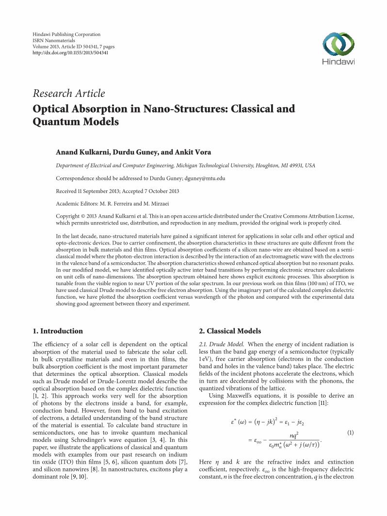
Figure 2 shows a plot of 120572119889(ℎ120596) versus ℎ120596 along with an
experimental plot for GaAs A very good agreement is seenbetween theory and experiment at low photon energies andthe discrepancy between experimental data and theory athigh photon energies may be due to free carrier absorptionas well
32 Nanostructures In order to improve the efficiency ofa solar cell one obvious choice is to use multiple bandgap devices to enable absorption of maximum number ofphotons of the solar spectrum These devices also calledldquotandemrdquo solar cells are discussed in the literature [14 15]Here the complexity of materials used the compatibility ofthe adjacent layers and the manufacturing difficulties lead tovery expensive devices for increased efficiency performance
An alternative way to boost optical absorption is touse nano structure based devices to attain multiple bandgaps based on the size of the quantum dots or quantumwells (based on quantum mechanics the size of the dot orwell determines the band gap of the material) Since thenanostructures of silicon result in direct band gap materialthe optical absorption is enhanced due to an increase ofoscillator strength We assumed a value of one for theoscillator strength of nanostructured silicon and the reducedmass is taken as half the mass of electron rest mass The bandgap energy is taken as 182 eV for a cluster of 18 atoms (aquantum dot of radius 1 nm) [16] Plugging the numbers in
005
115
225
335
445
5
14 15 16 17 18 19 2Photon energy (eV)
GaAs experimentalGaAs calculated plot
Abso
rptio
n co
effici
ent120572times10Eminus4
(cm
minus1)
Figure 2 Plot of 120572119889(ℎ120596) versus ℎ120596 along with an experimental [2]
plot for GaAs
0 200 400 600 8000
2
4
6
8
10
12
14
Refr
activ
e ind
ex120578
Wavelength 120582 (nm)
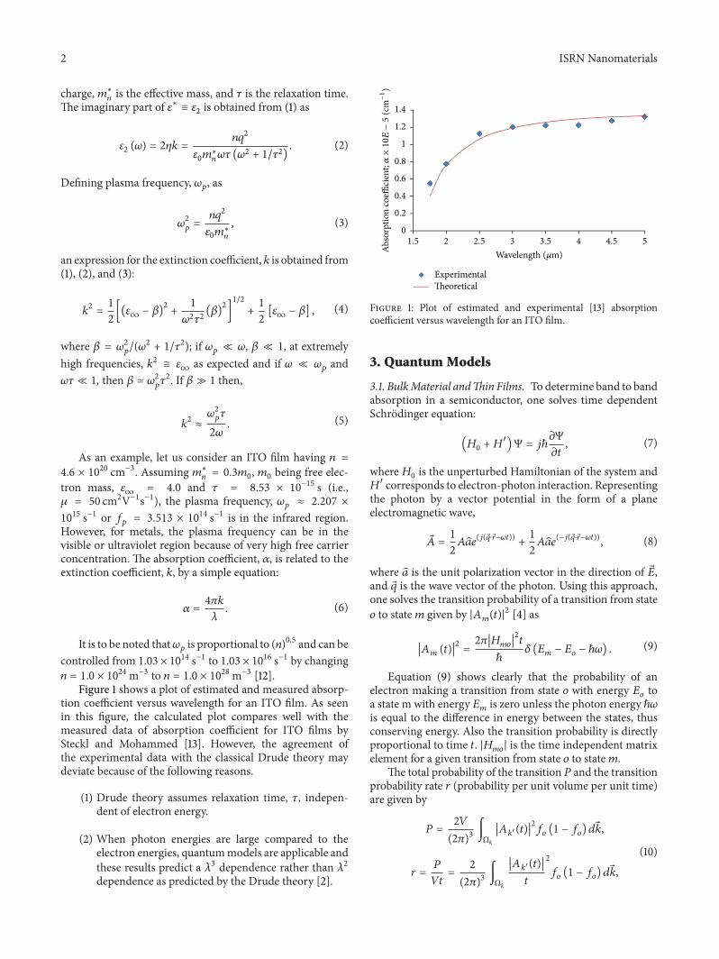
Figure 3 Plot of 120578(120582) versus wavelength for silicon
(13) we get an expression for the absorption coefficient fornano structured silicon as
120572119889cong
54 times 105
120578 (120582)
[
124
120582
minus 182]
12
(cmminus1) (15)
where 120582 is the incident photon wavelength in 120583m 120578(120582) is therefractive index given by Herzbergerrsquos formula
120578 (120582) = 32346 +
03698
1205822minus 0028
(16)
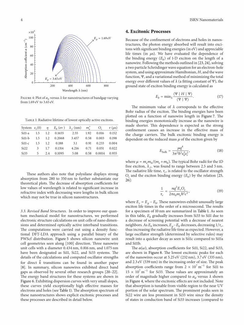
Figure 3 shows a plot of 120578(120582) versus 120582 based on (16) andFigure 4 shows a plot of 120572
119889versus 120582 for nanostructures of
bandgap varying from 169 eV to 365 eV (quantum dot sizevaries from 2 nm to 7 nm [17 18]) As seen in Figure 4 theabsorption coefficient 120572 quickly increases to 1 times 105 cmminus1for a quantum dot having 119864
119892= 169 eV Comparing 120572 values
in bulk silicon (less than 104 cmminus1) we observe an order ofmagnitude enhancement in 120572 Smith et al have performedtime resolved PL measurements on silicon nano-particles (sim1 nm) and have reported direct band to band transition withemission in the wavelength range of 400ndash480 nm supportingour estimated results [19]
4 ISRN Nanomaterials
200 400 600 8000
20
40
60
80
100
Abso
rptio
n co
ffici
ent120572
(cm
minus1)
Wavelength 120582 (nm)
times103
Eg = 169 eV
Eg = 365 eV
Figure 4 Plot of 120572119889versus 120582 for nanostructures of bandgap varying
from 169 eV to 365 eV
Table 1 Radiative lifetime of lowest optically active excitons
System 1205761(0) 120578 119864
119887(ev ) 120582
119891(nm) 119898
lowast
119890119874119904
120591 (120583s)Si11-a 15 12 01655 255 192 0016 0152Si11-b 15 12 02068 3457 058 0003 0198Si11-c 15 12 0188 31 091 0233 0004Si22 3 17 01314 4216 071 0051 0022Si33 5 24 01095 508 058 00014 0955
These authors also note that polysilane displays strongabsorption from 280 to 350 nm to further substantiate ourtheoretical plots The decrease of absorption coefficients forlow values of wavelength is related to significant increase inrefractive index with decreasing wave lengths in bulk siliconwhich may not be true in silicon nanostructures
33 Revised Band Structures In order to improve our quan-tum mechanical model for nanostructures we performedelectronic structure calculations on unit cells of nano dimen-sions and determined optically active interband transitionsThe computations were carried out using a density func-tional DFT-LDA approach using a parallel binary of thePWScf distribution Figure 5 shows silicon nanowire unitcell geometries seen along [100] direction Three nanowireunit cells with a diameter 0434 nm 0816 nm and 1075 nmhave been designated as Si11 Si22 and Si33 systems Thedetails of the calculations and computed oscillator strengthsfor direct
119896 transitions can be found in another paper[8] In summary silicon nanowires exhibited direct bandgaps as observed by several other research groups [20ndash22]The energy band structures for these systems are shown inFigure 6 Exhibiting dispersion curves with very small slopesthese curves yield exceptionally high effective masses forelectrons and holes (see Table 1) The absorption spectrum ofthese nanostructures shows explicit excitonic processes andthese processes are described in detail below
4 Excitonic Processes
Because of the confinement of electrons and holes in nanos-tructures the photon energy absorbed will result into exci-tons with significant binding energies (in eV) and appreciablelife times (in 120583s) We have evaluated the dependence ofthe binding energy (119864
119887) of 1-D exciton on the length of a
nanowire Following themethods outlined in [23 24] solvinga two particle Schrodingerwave equation for an electron-holesystem and using approximateHamiltonian119867 and thewavefunctionΨ and a variationalmethod ofminimizing the totalenergy over different values of 120582 (a fitting constant of Ψ) theground state of exciton binding energy is calculated as
119864119887= min
120582
⟨Ψ | 119867 | Ψ⟩
⟨Ψ | Ψ⟩
(17)
The minimum value of 120582 corresponds to the effectiveBohr radius of the exciton The binding energies have beenplotted on a function of nanowire length in Figure 7 Thebinding energies monotonically increase as the nanowire ismade shorter This dependence is expected as the strongconfinement causes an increase in the effective mass ofthe charge carriers The bulk excitonic binding energy isdependent on the reduced mass 120583 of the exciton given by
119864bulk =1205831199024
31205872ℎ21205762
01205762
119903
(18)
where 120583 = 119898119890119898ℎ(119898119890+119898ℎ) The typical Bohr radii for the 1D
free exciton 120582119891 was found to range between 25 and 5 nm
The radiative life time 120591119903 is related to the oscillator strength
119874119904and the exciton binding energy (119864
119887) by the relation [25
26]
1
120591119903
=
1198991199022
119864V119874119904
21205871205760119898119890ℎ21198883
(19)
where 119864V = 119864119892 minus 119864119887 These nanowires exhibit unusually largeexciton life times in the order of a microsecond The resultsfor a specimen of 10 nm are summarized in Table 1 As seenin this table 119864
119887gradually increases from Si33 to Si11 due to
a decrease of screening potential with a decrease of nearestneighbors As119864
119887increases119864
119892minus119864119887decreases decreasing 1120591
119903
thus increasing the radiative life time as expected However alarge oscillator strength (determined by selective rules) mayresult into a quicker decay as seen is Si11c compared to Si11aand Si11b
The 120572(120596) absorption coefficients for Si11 Si22 and Si33are shown in Figure 8 The lowest excitonic peaks for eachof the nanowires occur at 525 eV (232 nm) 37 eV (335 nm)and 23 eV (539 nm) in the increasing order of size The peakabsorption coefficients range from 2 times 10
7mminus1 for Si11 to15 times 10
7mminus1 for Si33 These values are approximately anorder of magnitude higher compared to 120572
119889versus 120582 shown
in Figure 4 where the excitonic effects are not included Notethat absorption is tunable from visible region to the near UVportion of the solar spectrum The prominent peaks seen inSi22 wire are less prominent in Si33 wire since the densityof states in conduction band of Si33 increases (compared to
ISRN Nanomaterials 5
x
y
z
(a)
x
y
z
(b)
x
y
z
(c)
Figure 5 Silicon nanowire unit cell geometries seen along [100] direction Three nanowire unit cells with a diameter 0434 nm 0816 nmand 1075 nm have been designated as (a) Si11 (b) Si22 and (c) Si33
minus10
minus8
minus6
minus4
minus2
0
2
Ener
gy (e
V)
0 02 04Kz middot 2120587a0
(a)
Ener
gy (e
V)
minus7
minus6
minus5
minus4
minus3
minus2
minus1
0
0 02 04Kz middot 2120587a0
(b)
Ener
gy (e
V)
0 02 04minus2
minus1
0
1
2
3
4
Kz middot 2120587a0
(c)
Figure 6 1-D band-structure of silicon nanowire system along the 119911-direction with 0 lt 119896119911 lt 1205871198860with 119886
0= 543 A being the lattice constant
Band diagrams are shown for (from left to right) Si11 Si22 and Si33 systems
Si22) thus decreasing the resonance effects Also the ripplednature of the absorption spectrum is less in Si33 comparedto Si22 Thus the absorption spectra of nanostructures aredominated by the excitonic processes
5 Conclusions
Drude model gives a fairly good explanation of the opticalabsorption by free carriers Though one could describe theexcitations of free electrons in the conduction band usingquantum mechanics the advantages are valid when photonenergies are significantly higher than electron energies For
band to band transition the quantum mechanical modelsdepicting the details of the band structures are essential tofully explain the observed absorption spectrum in bulk andthin film materials This approach is not adequate to explainthe optical absorption spectra in nanostructures which showresonant peaks and enhanced absorption Here electronicstructure calculations on unit cells of nano dimensions leadto excitonic processes that have a significant impact onabsorption The 119864 versus
119896 curves show weak dispersion innanostructures compared to those of bulk materials resultingin heavier effective masses for both electrons and holes Thebinding energies of excitons in nanostructures are a few
6 ISRN Nanomaterials
0 2 4 6 8 10 12Nanowire length (nm)
Exci
ton
bind
ing
ener
gy (e
V)
Si11aSi11bSi11c
Si22Si33
100
10minus1
Figure 7 1-D exciton binding energy in silicon nanowires as afunction of nanowire length
1 2 3 4 5 6 70
2
4
6
8
10
12
14
16
Energy (eV)
Si11Si22Si33
times107
120572(120596
) (m
minus1)
Figure 8 Optical absorption coefficient for the nanowire systems
tenths of eV compared to a few hundredths of eV in bulkmaterials (0015 eV in Si) The radiative life times are inmicroseconds in nanostructures as compared to nanosecondsas observed in direct bandgap semiconductors for exam-ple GaAs In nanostructures only certain transitions fromvalence band to conduction band dominate indicating largeoscillator strengths a measure on the strength of absorptionfor a given energy of photon Hence optical absorption in
nanostructures is a lot more complex phenomena than thatin bulk materials or thin films
Acknowledgment
This work was supported by the National Science Foundationunder grant CBET-1235750 We also would like to thankJaspreet Singh and Vidur Parkash for their help with thefigures
References
[1] P Y Yu and M Cardona Fundamentals of SemiconductorsSpringer New York NY USA 3rd edition 2001
[2] E D Palik Handbook of Optical Constants of Solids AcademicPress New York NY USA 1985
[3] R A Smith Semiconductors Cambridge University Press NewYork NY USA 2nd edition 1978
[4] C M Wolfe N Holonyak and G E Stillman Physical Proper-ties of Semiconductors Pentice Hall New Jersey NJ USA 1989
[5] S A Knickerbocker and A K Kulkarni ldquoEstimation andverification of the optical properties of indium tin oxide basedon the energy band diagramrdquo Journal of Vacuum Science andTechnology A vol 14 no 3 pp 757ndash761 1996
[6] A K Kulkarni and S A Knickerbocker ldquoEstimation andverification of the electrical properties of indium tin oxide basedon the energy band diagramrdquo Journal of Vacuum Science andTechnology A vol 14 no 3 pp 1709ndash1714 1996
[7] J S Nayyar and A Kulkarni ldquoOne aspect of solar cell efficiencymultiple wavelengths photon absorption in nano-silicon struc-turesrdquo in Proceedings of the SPIE Nanoscale Photonic and CellTechnologies for Photovoltaics II vol 7411 August 2009
[8] V Parkash and A K Kulkarni ldquoOptical absorption character-istics of silicon nanowires for photovoltaic applicationsrdquo IEEETransactions on Nanotechnology vol 10 no 6 pp 1293ndash12972011
[9] T Takagahara and K Takeda ldquoTheory of the quantum con-finement effect on excitons in quantum dots of indirect-gapmaterialsrdquo Physical Review B vol 46 no 23 pp 15578ndash155811992
[10] M Bruno M Palummo A Marini R Del Sole and S OssicinildquoFrom Si nanowires to porous silicon the role of excitoniceffectsrdquo Physical Review Letters vol 98 no 3 Article ID 0368072007
[11] P Y Yu and M Cardona Fundamentals of SemiconductorsSpringer New York NY USA 3rd edition 2001
[12] S A Knickerbocker Estimation and verification of electricaland optical properties of indium-tin-oxide based on energy banddiagrams [PhD thesis] Michigan Technological UniversityHoughton Mich USA 1995
[13] A J Steckl and G Mohammed ldquoThe effect of ambient atmo-sphere in the annealing of indium tin oxide filmsrdquo Journal ofApplied Physics vol 51 no 7 pp 3890ndash3895 1980
[14] M A Green Third Generation Photovoltaics Advanced SolarEnergy Conversion Springer Berlin Germany 2006
[15] J Nelson The Physics of Solar Cells Imperial College PressLondon UK 2003
[16] D C Johnson I M Ballard K W J Barnham et al ldquoObserva-tion of photon recycling in strain-balanced quantum well solarcellsrdquo Applied Physics Letters vol 90 no 21 Article ID 2135052007
ISRN Nanomaterials 7
[17] L Cuadra A Martı and A Luque ldquoType II broken bandheterostructure quantum dot to obtain a material for theintermediate band solar cellrdquo Physica E vol 14 no 1-2 pp 162ndash165 2002
[18] A Luque and A Martı ldquoUltra-high efficiency solar cells thepath formass penetration of solar electricityrdquoElectronics Lettersvol 44 no 16 p 943 2008
[19] A Smith ZH Yamani N Roberts et al ldquoObservation of strongdirect-like oscillator strength in the photoluminescence of Sinanoparticlesrdquo Physical Review B vol 72 no 20 Article ID205307 2005
[20] E C Garnett and P Yang ldquoSilicon nanowire radial p-n junctionsolar cellsrdquo Journal of the American Chemical Society vol 130no 29 pp 9224ndash9225 2008
[21] V Sivakov G Andra A Gawlik et al ldquoSilicon nanowire-based solar cells on glass synthesis optical properties and cellparametersrdquo Nano Letters vol 9 no 4 pp 1549ndash1554 2009
[22] J P Perdew and A Zunger ldquoSelf-interaction correction todensity-functional approximations for many-electron systemsrdquoPhysical Review B vol 23 no 10 pp 5048ndash5079 1981
[23] Y Cui X Duan J Hu and C M Lieber ldquoDoping and electricaltransport in silicon nanowiresrdquo Journal of Physical Chemistry Bvol 104 no 22 pp 5215ndash5216 2000
[24] A Poruba J Springer L Mullerova et al ldquoTemperature depen-dence of the optical absorption coefficient of microcrystallinesiliconrdquo Journal of Non-Crystalline Solids vol 338ndash340 no 1pp 222ndash227 2004
[25] PMDerlett T C Choy andAM Stoneham ldquoAn investigationof the porous silicon optical absorption power lawnear the bandedgerdquo Journal of Physics vol 7 no 12 pp 2507ndash2523 1995
[26] G Bastard E E Mendez L L Chang and L Esaki ldquoExcitonbinding energy in quantum wellsrdquo Physical Review B vol 26no 4 pp 1974ndash1979 1982
Submit your manuscripts athttpwwwhindawicom
ScientificaHindawi Publishing Corporationhttpwwwhindawicom Volume 2014
CorrosionInternational Journal of
Hindawi Publishing Corporationhttpwwwhindawicom Volume 2014
Polymer ScienceInternational Journal of
Hindawi Publishing Corporationhttpwwwhindawicom Volume 2014
Hindawi Publishing Corporationhttpwwwhindawicom Volume 2014
CeramicsJournal of
Hindawi Publishing Corporationhttpwwwhindawicom Volume 2014
CompositesJournal of
NanoparticlesJournal of
Hindawi Publishing Corporationhttpwwwhindawicom Volume 2014
Hindawi Publishing Corporationhttpwwwhindawicom Volume 2014
International Journal of
Biomaterials
Hindawi Publishing Corporationhttpwwwhindawicom Volume 2014
NanoscienceJournal of
TextilesHindawi Publishing Corporation httpwwwhindawicom Volume 2014
Journal of
NanotechnologyHindawi Publishing Corporationhttpwwwhindawicom Volume 2014
Journal of
CrystallographyJournal of
Hindawi Publishing Corporationhttpwwwhindawicom Volume 2014
The Scientific World JournalHindawi Publishing Corporation httpwwwhindawicom Volume 2014
Hindawi Publishing Corporationhttpwwwhindawicom Volume 2014
CoatingsJournal of
Advances in
Materials Science and EngineeringHindawi Publishing Corporationhttpwwwhindawicom Volume 2014
Smart Materials Research
Hindawi Publishing Corporationhttpwwwhindawicom Volume 2014
Hindawi Publishing Corporationhttpwwwhindawicom Volume 2014
MetallurgyJournal of
Hindawi Publishing Corporationhttpwwwhindawicom Volume 2014
BioMed Research International
MaterialsJournal of
Hindawi Publishing Corporationhttpwwwhindawicom Volume 2014
Nano
materials
Hindawi Publishing Corporationhttpwwwhindawicom Volume 2014
Journal ofNanomaterials
2 ISRN Nanomaterials
charge 119898lowast119899is the effective mass and 120591 is the relaxation time
The imaginary part of 120576lowast equiv 1205762is obtained from (1) as
1205762(120596) = 2120578119896 =
1198991199022
1205760119898lowast
119899120596120591 (120596
2+ 11205912)
(2)
Defining plasma frequency 120596119901 as
1205962
119901=
1198991199022
1205760119898lowast
119899
(3)
an expression for the extinction coefficient 119896 is obtained from(1) (2) and (3)
1198962
=
1
2
[(120576infinminus 120573)2
+
1
12059621205912
(120573)2
]
12
+
1
2
[120576infinminus 120573] (4)
where 120573 = 1205962119901(1205962
+ 11205912
) if 120596119901≪ 120596 120573 ≪ 1 at extremely
high frequencies 1198962 cong 120576infin
as expected and if 120596 ≪ 120596119901and
120596120591 ≪ 1 then 120573 ≃ 12059621199011205912 If 120573 ≫ 1 then
1198962
asymp
1205962
119901120591
2120596
(5)
As an example let us consider an ITO film having 119899 =46 times 10
20 cmminus3 Assuming 119898lowast119899= 03119898
0 1198980being free elec-
tron mass 120576infin
= 40 and 120591 = 853 times 10minus15 s (ie
120583 = 50 cm2Vminus1sminus1) the plasma frequency 120596119901asymp 2207 times
1015 sminus1 or 119891
119901= 3513 times 10
14 sminus1 is in the infrared regionHowever for metals the plasma frequency can be in thevisible or ultraviolet region because of very high free carrierconcentration The absorption coefficient 120572 is related to theextinction coefficient 119896 by a simple equation
120572 =
4120587119896
120582
(6)
It is to be noted that120596119901is proportional to (119899)05 and can be
controlled from 103 times 1014 sminus1 to 103 times 1016 sminus1 by changing119899 = 10 times 10
24mminus3 to 119899 = 10 times 1028mminus3 [12]Figure 1 shows a plot of estimated and measured absorp-
tion coefficient versus wavelength for an ITO film As seenin this figure the calculated plot compares well with themeasured data of absorption coefficient for ITO films bySteckl and Mohammed [13] However the agreement ofthe experimental data with the classical Drude theory maydeviate because of the following reasons
(1) Drude theory assumes relaxation time 120591 indepen-dent of electron energy
(2) When photon energies are large compared to theelectron energies quantummodels are applicable andthese results predict a 1205823 dependence rather than 1205822dependence as predicted by the Drude theory [2]
0
02
04
06
08
1
12
14
15 2 25 3 35 4 45 5Wavelength (120583m)
ExperimentalTheoretical
Abso
rptio
n co
effici
ent120572times10Eminus5
(cm
minus1)
Figure 1 Plot of estimated and experimental [13] absorptioncoefficient versus wavelength for an ITO film
3 Quantum Models
31 BulkMaterial andThin Films To determine band to bandabsorption in a semiconductor one solves time dependentSchrodinger equation
(1198670+ 1198671015840
)Ψ = 119895ℎ
120597Ψ
120597119905
(7)
where1198670is the unperturbed Hamiltonian of the system and
1198671015840 corresponds to electron-photon interaction Representing
the photon by a vector potential in the form of a planeelectromagnetic wave
=
1
2
119860119886119890(119895( 119902sdot 119903minus120596119905))
+
1
2
119860119886119890(minus119895( 119902sdot 119903minus120596119905))
(8)
where 119886 is the unit polarization vector in the direction of and 119902 is the wave vector of the photon Using this approachone solves the transition probability of a transition from state119900 to state119898 given by |119860
119898(119905)|2 [4] as
1003816100381610038161003816119860119898(119905)1003816100381610038161003816
2
=
21205871003816100381610038161003816119867119898119900
1003816100381610038161003816
2
119905
ℎ
120575 (119864119898minus 119864119900minus ℎ120596)
(9)
Equation (9) shows clearly that the probability of anelectron making a transition from state 119900 with energy 119864
119900to
a state m with energy 119864119898is zero unless the photon energy ℎ120596
is equal to the difference in energy between the states thusconserving energy Also the transition probability is directlyproportional to time 119905 |119867
119898119900| is the time independent matrix
element for a given transition from state 119900 to state119898The total probability of the transition 119875 and the transition
probability rate 119903 (probability per unit volume per unit time)are given by
119875 =
2119881
(2120587)3int
Ω119896
10038161003816100381610038161198601198961015840(119905)1003816100381610038161003816
2
119891119900(1 minus 119891
119900) 119889
119896
119903 =
119875
119881119905
=
2
(2120587)3int
Ω119896
10038161003816100381610038161198601198961015840(119905)1003816100381610038161003816
119905
2
119891119900(1 minus 119891
119900) 119889
119896
(10)
ISRN Nanomaterials 3
where 119881 is the crystal volume and 119891119900is the Fermi Dirac dis-
tribution function Expressing |1198601198961015840(119905)|2 as a sum of allowed
and forbidden transitions it is possible to reduce the allowedHamiltonian to minus(1199021198602119898)( 119886 sdot
1198961198961015840) Thus 119903allowed is given by
119903allowed =1199022
1198602
120596119874119904(2119898119903)32
8120587ℎ3119898
119891119900(1 minus 119891
119900)radicℎ120596 minus 119864
119892
(11)
where 119874119904is the oscillator strength a dimensionless quantity
defined as
119874119904=
2 ( 119886 sdot 1198961198961015840)
ℎ119898120596
(12)
This oscillator strength for a given transition can varyfrom very low values (10minus5) to 1 depending upon the selectionrules It is significantly higher in direct semiconductors likeGaAs Absorption coefficient 120572
119889 is defined as the transition
rate per unit quantum flux (quantum flux is defined as thenumber of incident photons per unit time) 120572
119889equiv 120572 for direct
band gap semiconductor
120572119889=
1199022
119874119904(2119898119903)
41205871205760119888120578ℎ2119898
32
119891119900(1 minus 119891
119900)radicℎ120596 minus 119864
119892 (13)
where 119898119903is the reduced mass and 120578 is the refractive index
Substituting the values for the constants for GaAs we get
120572119889(ℎ120596) =
15 times 105
radicℎ120596 minus 119864119892
120578 (120582)
(cmminus1) (14)
Figure 2 shows a plot of 120572119889(ℎ120596) versus ℎ120596 along with an
experimental plot for GaAs A very good agreement is seenbetween theory and experiment at low photon energies andthe discrepancy between experimental data and theory athigh photon energies may be due to free carrier absorptionas well
32 Nanostructures In order to improve the efficiency ofa solar cell one obvious choice is to use multiple bandgap devices to enable absorption of maximum number ofphotons of the solar spectrum These devices also calledldquotandemrdquo solar cells are discussed in the literature [14 15]Here the complexity of materials used the compatibility ofthe adjacent layers and the manufacturing difficulties lead tovery expensive devices for increased efficiency performance
An alternative way to boost optical absorption is touse nano structure based devices to attain multiple bandgaps based on the size of the quantum dots or quantumwells (based on quantum mechanics the size of the dot orwell determines the band gap of the material) Since thenanostructures of silicon result in direct band gap materialthe optical absorption is enhanced due to an increase ofoscillator strength We assumed a value of one for theoscillator strength of nanostructured silicon and the reducedmass is taken as half the mass of electron rest mass The bandgap energy is taken as 182 eV for a cluster of 18 atoms (aquantum dot of radius 1 nm) [16] Plugging the numbers in
005
115
225
335
445
5
14 15 16 17 18 19 2Photon energy (eV)
GaAs experimentalGaAs calculated plot
Abso
rptio
n co
effici
ent120572times10Eminus4
(cm
minus1)
Figure 2 Plot of 120572119889(ℎ120596) versus ℎ120596 along with an experimental [2]
plot for GaAs
0 200 400 600 8000
2
4
6
8
10
12
14
Refr
activ
e ind
ex120578
Wavelength 120582 (nm)
Figure 3 Plot of 120578(120582) versus wavelength for silicon
(13) we get an expression for the absorption coefficient fornano structured silicon as
120572119889cong
54 times 105
120578 (120582)
[
124
120582
minus 182]
12
(cmminus1) (15)
where 120582 is the incident photon wavelength in 120583m 120578(120582) is therefractive index given by Herzbergerrsquos formula
120578 (120582) = 32346 +
03698
1205822minus 0028
(16)
Figure 3 shows a plot of 120578(120582) versus 120582 based on (16) andFigure 4 shows a plot of 120572
119889versus 120582 for nanostructures of
bandgap varying from 169 eV to 365 eV (quantum dot sizevaries from 2 nm to 7 nm [17 18]) As seen in Figure 4 theabsorption coefficient 120572 quickly increases to 1 times 105 cmminus1for a quantum dot having 119864
119892= 169 eV Comparing 120572 values
in bulk silicon (less than 104 cmminus1) we observe an order ofmagnitude enhancement in 120572 Smith et al have performedtime resolved PL measurements on silicon nano-particles (sim1 nm) and have reported direct band to band transition withemission in the wavelength range of 400ndash480 nm supportingour estimated results [19]
4 ISRN Nanomaterials
200 400 600 8000
20
40
60
80
100
Abso
rptio
n co
ffici
ent120572
(cm
minus1)
Wavelength 120582 (nm)
times103
Eg = 169 eV
Eg = 365 eV
Figure 4 Plot of 120572119889versus 120582 for nanostructures of bandgap varying
from 169 eV to 365 eV
Table 1 Radiative lifetime of lowest optically active excitons
System 1205761(0) 120578 119864
119887(ev ) 120582
119891(nm) 119898
lowast
119890119874119904
120591 (120583s)Si11-a 15 12 01655 255 192 0016 0152Si11-b 15 12 02068 3457 058 0003 0198Si11-c 15 12 0188 31 091 0233 0004Si22 3 17 01314 4216 071 0051 0022Si33 5 24 01095 508 058 00014 0955
These authors also note that polysilane displays strongabsorption from 280 to 350 nm to further substantiate ourtheoretical plots The decrease of absorption coefficients forlow values of wavelength is related to significant increase inrefractive index with decreasing wave lengths in bulk siliconwhich may not be true in silicon nanostructures
33 Revised Band Structures In order to improve our quan-tum mechanical model for nanostructures we performedelectronic structure calculations on unit cells of nano dimen-sions and determined optically active interband transitionsThe computations were carried out using a density func-tional DFT-LDA approach using a parallel binary of thePWScf distribution Figure 5 shows silicon nanowire unitcell geometries seen along [100] direction Three nanowireunit cells with a diameter 0434 nm 0816 nm and 1075 nmhave been designated as Si11 Si22 and Si33 systems Thedetails of the calculations and computed oscillator strengthsfor direct
119896 transitions can be found in another paper[8] In summary silicon nanowires exhibited direct bandgaps as observed by several other research groups [20ndash22]The energy band structures for these systems are shown inFigure 6 Exhibiting dispersion curves with very small slopesthese curves yield exceptionally high effective masses forelectrons and holes (see Table 1) The absorption spectrum ofthese nanostructures shows explicit excitonic processes andthese processes are described in detail below
4 Excitonic Processes
Because of the confinement of electrons and holes in nanos-tructures the photon energy absorbed will result into exci-tons with significant binding energies (in eV) and appreciablelife times (in 120583s) We have evaluated the dependence ofthe binding energy (119864
119887) of 1-D exciton on the length of a
nanowire Following themethods outlined in [23 24] solvinga two particle Schrodingerwave equation for an electron-holesystem and using approximateHamiltonian119867 and thewavefunctionΨ and a variationalmethod ofminimizing the totalenergy over different values of 120582 (a fitting constant of Ψ) theground state of exciton binding energy is calculated as
119864119887= min
120582
⟨Ψ | 119867 | Ψ⟩
⟨Ψ | Ψ⟩
(17)
The minimum value of 120582 corresponds to the effectiveBohr radius of the exciton The binding energies have beenplotted on a function of nanowire length in Figure 7 Thebinding energies monotonically increase as the nanowire ismade shorter This dependence is expected as the strongconfinement causes an increase in the effective mass ofthe charge carriers The bulk excitonic binding energy isdependent on the reduced mass 120583 of the exciton given by
119864bulk =1205831199024
31205872ℎ21205762
01205762
119903
(18)
where 120583 = 119898119890119898ℎ(119898119890+119898ℎ) The typical Bohr radii for the 1D
free exciton 120582119891 was found to range between 25 and 5 nm
The radiative life time 120591119903 is related to the oscillator strength
119874119904and the exciton binding energy (119864
119887) by the relation [25
26]
1
120591119903
=
1198991199022
119864V119874119904
21205871205760119898119890ℎ21198883
(19)
where 119864V = 119864119892 minus 119864119887 These nanowires exhibit unusually largeexciton life times in the order of a microsecond The resultsfor a specimen of 10 nm are summarized in Table 1 As seenin this table 119864
119887gradually increases from Si33 to Si11 due to
a decrease of screening potential with a decrease of nearestneighbors As119864
119887increases119864
119892minus119864119887decreases decreasing 1120591
119903
thus increasing the radiative life time as expected However alarge oscillator strength (determined by selective rules) mayresult into a quicker decay as seen is Si11c compared to Si11aand Si11b
The 120572(120596) absorption coefficients for Si11 Si22 and Si33are shown in Figure 8 The lowest excitonic peaks for eachof the nanowires occur at 525 eV (232 nm) 37 eV (335 nm)and 23 eV (539 nm) in the increasing order of size The peakabsorption coefficients range from 2 times 10
7mminus1 for Si11 to15 times 10
7mminus1 for Si33 These values are approximately anorder of magnitude higher compared to 120572
119889versus 120582 shown
in Figure 4 where the excitonic effects are not included Notethat absorption is tunable from visible region to the near UVportion of the solar spectrum The prominent peaks seen inSi22 wire are less prominent in Si33 wire since the densityof states in conduction band of Si33 increases (compared to
ISRN Nanomaterials 5
x
y
z
(a)
x
y
z
(b)
x
y
z
(c)
Figure 5 Silicon nanowire unit cell geometries seen along [100] direction Three nanowire unit cells with a diameter 0434 nm 0816 nmand 1075 nm have been designated as (a) Si11 (b) Si22 and (c) Si33
minus10
minus8
minus6
minus4
minus2
0
2
Ener
gy (e
V)
0 02 04Kz middot 2120587a0
(a)
Ener
gy (e
V)
minus7
minus6
minus5
minus4
minus3
minus2
minus1
0
0 02 04Kz middot 2120587a0
(b)
Ener
gy (e
V)
0 02 04minus2
minus1
0
1
2
3
4
Kz middot 2120587a0
(c)
Figure 6 1-D band-structure of silicon nanowire system along the 119911-direction with 0 lt 119896119911 lt 1205871198860with 119886
0= 543 A being the lattice constant
Band diagrams are shown for (from left to right) Si11 Si22 and Si33 systems
Si22) thus decreasing the resonance effects Also the ripplednature of the absorption spectrum is less in Si33 comparedto Si22 Thus the absorption spectra of nanostructures aredominated by the excitonic processes
5 Conclusions
Drude model gives a fairly good explanation of the opticalabsorption by free carriers Though one could describe theexcitations of free electrons in the conduction band usingquantum mechanics the advantages are valid when photonenergies are significantly higher than electron energies For
band to band transition the quantum mechanical modelsdepicting the details of the band structures are essential tofully explain the observed absorption spectrum in bulk andthin film materials This approach is not adequate to explainthe optical absorption spectra in nanostructures which showresonant peaks and enhanced absorption Here electronicstructure calculations on unit cells of nano dimensions leadto excitonic processes that have a significant impact onabsorption The 119864 versus
119896 curves show weak dispersion innanostructures compared to those of bulk materials resultingin heavier effective masses for both electrons and holes Thebinding energies of excitons in nanostructures are a few
6 ISRN Nanomaterials
0 2 4 6 8 10 12Nanowire length (nm)
Exci
ton
bind
ing
ener
gy (e
V)
Si11aSi11bSi11c
Si22Si33
100
10minus1
Figure 7 1-D exciton binding energy in silicon nanowires as afunction of nanowire length
1 2 3 4 5 6 70
2
4
6
8
10
12
14
16
Energy (eV)
Si11Si22Si33
times107
120572(120596
) (m
minus1)
Figure 8 Optical absorption coefficient for the nanowire systems
tenths of eV compared to a few hundredths of eV in bulkmaterials (0015 eV in Si) The radiative life times are inmicroseconds in nanostructures as compared to nanosecondsas observed in direct bandgap semiconductors for exam-ple GaAs In nanostructures only certain transitions fromvalence band to conduction band dominate indicating largeoscillator strengths a measure on the strength of absorptionfor a given energy of photon Hence optical absorption in
nanostructures is a lot more complex phenomena than thatin bulk materials or thin films
Acknowledgment
This work was supported by the National Science Foundationunder grant CBET-1235750 We also would like to thankJaspreet Singh and Vidur Parkash for their help with thefigures
References
[1] P Y Yu and M Cardona Fundamentals of SemiconductorsSpringer New York NY USA 3rd edition 2001
[2] E D Palik Handbook of Optical Constants of Solids AcademicPress New York NY USA 1985
[3] R A Smith Semiconductors Cambridge University Press NewYork NY USA 2nd edition 1978
[4] C M Wolfe N Holonyak and G E Stillman Physical Proper-ties of Semiconductors Pentice Hall New Jersey NJ USA 1989
[5] S A Knickerbocker and A K Kulkarni ldquoEstimation andverification of the optical properties of indium tin oxide basedon the energy band diagramrdquo Journal of Vacuum Science andTechnology A vol 14 no 3 pp 757ndash761 1996
[6] A K Kulkarni and S A Knickerbocker ldquoEstimation andverification of the electrical properties of indium tin oxide basedon the energy band diagramrdquo Journal of Vacuum Science andTechnology A vol 14 no 3 pp 1709ndash1714 1996
[7] J S Nayyar and A Kulkarni ldquoOne aspect of solar cell efficiencymultiple wavelengths photon absorption in nano-silicon struc-turesrdquo in Proceedings of the SPIE Nanoscale Photonic and CellTechnologies for Photovoltaics II vol 7411 August 2009
[8] V Parkash and A K Kulkarni ldquoOptical absorption character-istics of silicon nanowires for photovoltaic applicationsrdquo IEEETransactions on Nanotechnology vol 10 no 6 pp 1293ndash12972011
[9] T Takagahara and K Takeda ldquoTheory of the quantum con-finement effect on excitons in quantum dots of indirect-gapmaterialsrdquo Physical Review B vol 46 no 23 pp 15578ndash155811992
[10] M Bruno M Palummo A Marini R Del Sole and S OssicinildquoFrom Si nanowires to porous silicon the role of excitoniceffectsrdquo Physical Review Letters vol 98 no 3 Article ID 0368072007
[11] P Y Yu and M Cardona Fundamentals of SemiconductorsSpringer New York NY USA 3rd edition 2001
[12] S A Knickerbocker Estimation and verification of electricaland optical properties of indium-tin-oxide based on energy banddiagrams [PhD thesis] Michigan Technological UniversityHoughton Mich USA 1995
[13] A J Steckl and G Mohammed ldquoThe effect of ambient atmo-sphere in the annealing of indium tin oxide filmsrdquo Journal ofApplied Physics vol 51 no 7 pp 3890ndash3895 1980
[14] M A Green Third Generation Photovoltaics Advanced SolarEnergy Conversion Springer Berlin Germany 2006
[15] J Nelson The Physics of Solar Cells Imperial College PressLondon UK 2003
[16] D C Johnson I M Ballard K W J Barnham et al ldquoObserva-tion of photon recycling in strain-balanced quantum well solarcellsrdquo Applied Physics Letters vol 90 no 21 Article ID 2135052007
ISRN Nanomaterials 7
[17] L Cuadra A Martı and A Luque ldquoType II broken bandheterostructure quantum dot to obtain a material for theintermediate band solar cellrdquo Physica E vol 14 no 1-2 pp 162ndash165 2002
[18] A Luque and A Martı ldquoUltra-high efficiency solar cells thepath formass penetration of solar electricityrdquoElectronics Lettersvol 44 no 16 p 943 2008
[19] A Smith ZH Yamani N Roberts et al ldquoObservation of strongdirect-like oscillator strength in the photoluminescence of Sinanoparticlesrdquo Physical Review B vol 72 no 20 Article ID205307 2005
[20] E C Garnett and P Yang ldquoSilicon nanowire radial p-n junctionsolar cellsrdquo Journal of the American Chemical Society vol 130no 29 pp 9224ndash9225 2008
[21] V Sivakov G Andra A Gawlik et al ldquoSilicon nanowire-based solar cells on glass synthesis optical properties and cellparametersrdquo Nano Letters vol 9 no 4 pp 1549ndash1554 2009
[22] J P Perdew and A Zunger ldquoSelf-interaction correction todensity-functional approximations for many-electron systemsrdquoPhysical Review B vol 23 no 10 pp 5048ndash5079 1981
[23] Y Cui X Duan J Hu and C M Lieber ldquoDoping and electricaltransport in silicon nanowiresrdquo Journal of Physical Chemistry Bvol 104 no 22 pp 5215ndash5216 2000
[24] A Poruba J Springer L Mullerova et al ldquoTemperature depen-dence of the optical absorption coefficient of microcrystallinesiliconrdquo Journal of Non-Crystalline Solids vol 338ndash340 no 1pp 222ndash227 2004
[25] PMDerlett T C Choy andAM Stoneham ldquoAn investigationof the porous silicon optical absorption power lawnear the bandedgerdquo Journal of Physics vol 7 no 12 pp 2507ndash2523 1995
[26] G Bastard E E Mendez L L Chang and L Esaki ldquoExcitonbinding energy in quantum wellsrdquo Physical Review B vol 26no 4 pp 1974ndash1979 1982
Submit your manuscripts athttpwwwhindawicom
ScientificaHindawi Publishing Corporationhttpwwwhindawicom Volume 2014
CorrosionInternational Journal of
Hindawi Publishing Corporationhttpwwwhindawicom Volume 2014
Polymer ScienceInternational Journal of
Hindawi Publishing Corporationhttpwwwhindawicom Volume 2014
Hindawi Publishing Corporationhttpwwwhindawicom Volume 2014
CeramicsJournal of
Hindawi Publishing Corporationhttpwwwhindawicom Volume 2014
CompositesJournal of
NanoparticlesJournal of
Hindawi Publishing Corporationhttpwwwhindawicom Volume 2014
Hindawi Publishing Corporationhttpwwwhindawicom Volume 2014
International Journal of
Biomaterials
Hindawi Publishing Corporationhttpwwwhindawicom Volume 2014
NanoscienceJournal of
TextilesHindawi Publishing Corporation httpwwwhindawicom Volume 2014
Journal of
NanotechnologyHindawi Publishing Corporationhttpwwwhindawicom Volume 2014
Journal of
CrystallographyJournal of
Hindawi Publishing Corporationhttpwwwhindawicom Volume 2014
The Scientific World JournalHindawi Publishing Corporation httpwwwhindawicom Volume 2014
Hindawi Publishing Corporationhttpwwwhindawicom Volume 2014
CoatingsJournal of
Advances in
Materials Science and EngineeringHindawi Publishing Corporationhttpwwwhindawicom Volume 2014
Smart Materials Research
Hindawi Publishing Corporationhttpwwwhindawicom Volume 2014
Hindawi Publishing Corporationhttpwwwhindawicom Volume 2014
MetallurgyJournal of
Hindawi Publishing Corporationhttpwwwhindawicom Volume 2014
BioMed Research International
MaterialsJournal of
Hindawi Publishing Corporationhttpwwwhindawicom Volume 2014
Nano
materials
Hindawi Publishing Corporationhttpwwwhindawicom Volume 2014
Journal ofNanomaterials
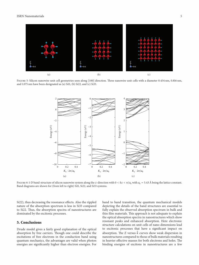
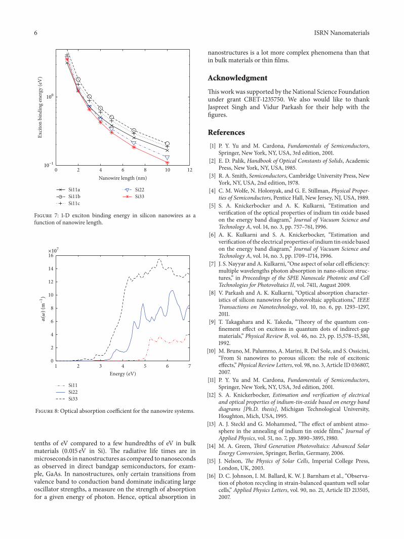
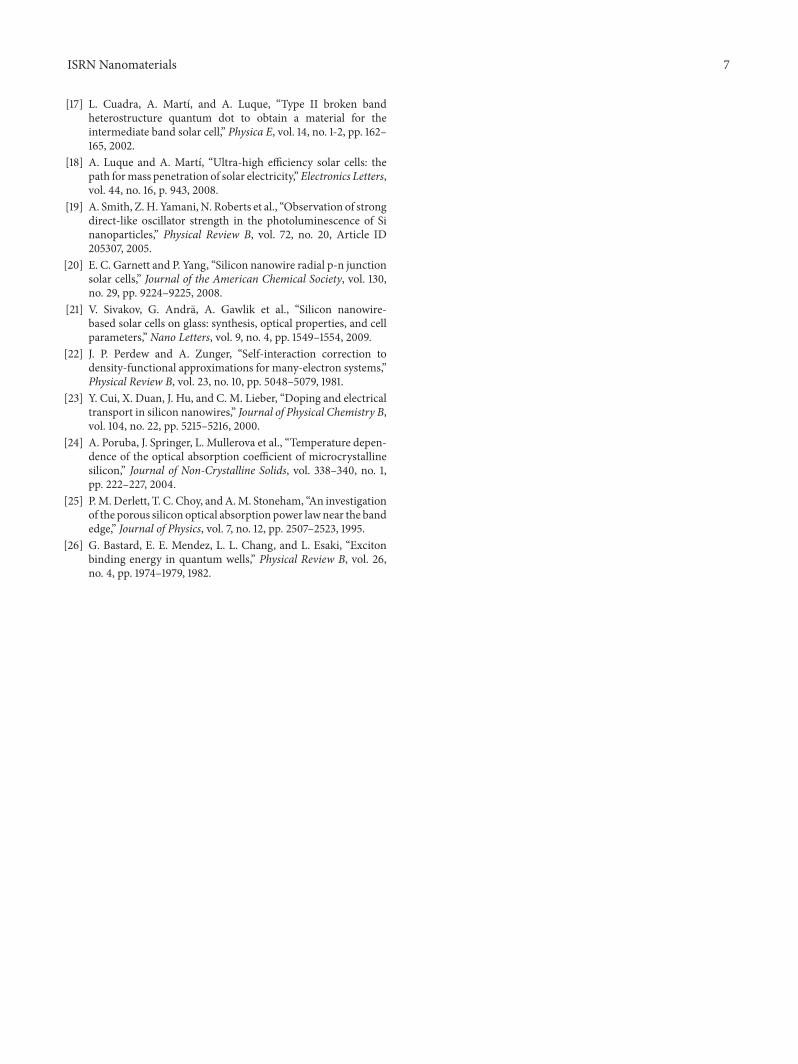