Embed Size (px)
Citation preview
SURFACE AND INTERFACE ANALYSISSurf. Interface Anal. 2001; 31: 909–914
Optical characterization techniques for processmonitoring†
C. Pickering∗
QinetiQ, St Andrews Road, Malvern, Worcs WR14 3PS, UK
Received 30 April 2001; Revised 14 May 2001; Accepted 21 May 2001
The aim of this special issue is to bring to the attention of the surface science community the potentialand application of optical techniques. This paper gives an overview of the major optical characterizationtechniques and the subsequent papers. Where possible, links with other surface science techniques arediscussed and the use of optical methods for process monitoring and control is emphasized. CrownCopyright 2001. Published by John Wiley & Sons, Ltd.
INTRODUCTION
According to Dataquest, about $2.3 billion is spent annuallyon process control equipment.1 This is dominated bypatterned wafer inspection of defects and critical dimensionscanning electron microscopy (CD-SEM) for monitoring andcontrol of lithography and etch processes. However, about$120 million is spent on ‘optical metrology’ equipment.This indicates the importance of optical-based techniquesin mainstream semiconductor processing, as well as forresearch and development in new material systems. Thereasons are obvious: optical methods are non-invasive andnon-destructive and can be used in any environment. Thus,measurements may be made on actual product wafers,which are increasing in size and cost, without wastage.The rapid increase in computing power also has stimulatedthe wider use of optical techniques for the rapid extractionof meaningful data, because the techniques generally areindirect and require significant data processing.
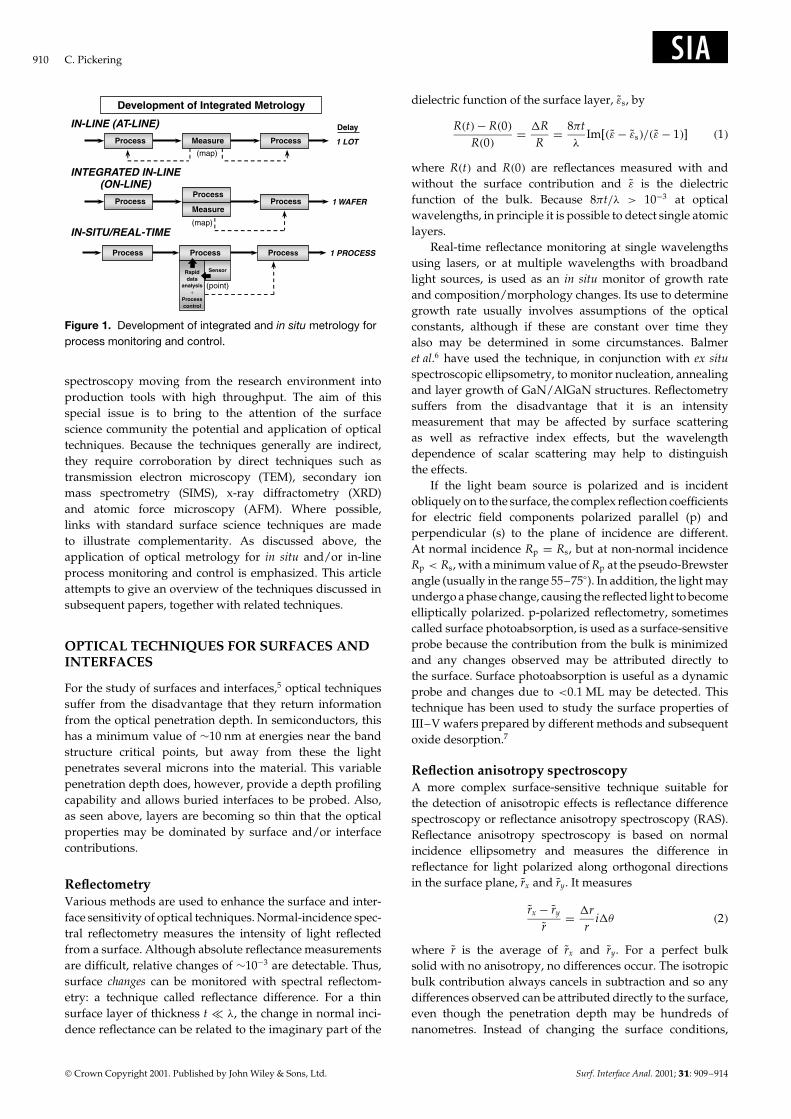
The various ways in which metrology techniques maybe used are indicated in Fig. 1. Until recently, most char-acterization was carried out off-line on monitor wafers.Thus, specially designed wafers are removed from process-ing equipment, measurements are made, which are oftendestructive, and data are fed back to the process equip-ment manually. This can take up to several days but hasthe advantage that the characterization tool can be usedfor many different processing equipments. Semiconductorprocessing fabrication lines have begun to introduce in-linemonitoring tools, which usually are dedicated to a particularprocess and can measure each batch of wafers as they areproduced. These usually are designed to measure productwafers, which allows more rapid feedback of the results tocorrect any drift out of specification and also feed-forwardto allow modifications in subsequent process conditions toaccommodate any unexpected changes. Optical techniques
ŁCorrespondence to: C. Pickering, QinetiQ, St Andrews Road,Malvern, Worcs WR14 3PS, UK.†Published with the permission of the Defence Evaluation andResearch Agency on behalf of the Controller of HMSO.
have the potential to make measurements very rapidly andtherefore may be used for real-time monitoring or control.2
In this mode, the sensor is attached to the process cham-ber and measurements made during the process itself. Theprocess rate determines the requirement for measurementspeed. Many deposition and etching processes take placeat rates of 0.1–1 nm s�1. This means that the measurementand data analysis must be made in the timescale of 0.2–2 s,otherwise the measurement will return an average valueover several monolayers and be too late to achieve real-timecontrol. Implementation of in situ real-time monitoring isdifficult in commercial systems because optical access oftenis impossible without substantial hardware modification. Anintermediate step is under development in which a moni-toring system is attached to a separate chamber within thetool (see Fig. 1 and the article by the author on spectroscopicellipsometry3). This allows the measurement of every wafer,or even every process if several processes are performed inthe same tool. This is useful for rapid process development,evaluation of surface cleaning, characterization of depositedlayers without exposure to the atmosphere and, ultimately,run-to-run control.
The Semiconductor Industry Association Roadmap4 hasidentified several important challenges for future metrol-ogy requirements. Shrinking feature sizes will introducerequirements for new materials and processes. In particular,complex multilayer stacks for gate and capacitor dielectricscomprising oxynitrides, oxide/nitride/oxide, Ta2O5, etc.need to be characterized as well as metals and silicides.Another challenge is due to the forthcoming approach of sta-tistical limits. As dimensions of structures and thicknessesof layers decrease, the finite dimensions of the atoms willlead to statistical variations, e.g. in gate dielectric structuresin which each layer is only a few atoms thick. The Roadmapalso identifies integrated in situ and in-line metrology (asdiscussed above) as a key requirement.
Thus, optical techniques are acquiring more importance,both for R&D and in production. The last few yearshave seen techniques such as spectroscopic ellipsometry,reflectometry, scatterometry, photoluminescence and Raman
DOI: 10.1002/sia.1128 Crown Copyright 2001. Published by John Wiley & Sons, Ltd.
910 C. Pickering
INTEGRATED IN-LINE(ON-LINE)
ProcessProcess
ProcessMeasure
IN-SITU/REAL-TIME
Process Process Process
Rapiddata
analysis+
Processcontrol
Sensor
Process Measure Process
IN-LINE (AT-LINE)
Development of Integrated Metrology
Delay
1 LOT
1 WAFER
1 PROCESS
(map)
(map)
(point)
Figure 1. Development of integrated and in situ metrology forprocess monitoring and control.
spectroscopy moving from the research environment intoproduction tools with high throughput. The aim of thisspecial issue is to bring to the attention of the surfacescience community the potential and application of opticaltechniques. Because the techniques generally are indirect,they require corroboration by direct techniques such astransmission electron microscopy (TEM), secondary ionmass spectrometry (SIMS), x-ray diffractometry (XRD)and atomic force microscopy (AFM). Where possible,links with standard surface science techniques are madeto illustrate complementarity. As discussed above, theapplication of optical metrology for in situ and/or in-lineprocess monitoring and control is emphasized. This articleattempts to give an overview of the techniques discussed insubsequent papers, together with related techniques.
OPTICAL TECHNIQUES FOR SURFACES ANDINTERFACES
For the study of surfaces and interfaces,5 optical techniquessuffer from the disadvantage that they return informationfrom the optical penetration depth. In semiconductors, thishas a minimum value of ¾10 nm at energies near the bandstructure critical points, but away from these the lightpenetrates several microns into the material. This variablepenetration depth does, however, provide a depth profilingcapability and allows buried interfaces to be probed. Also,as seen above, layers are becoming so thin that the opticalproperties may be dominated by surface and/or interfacecontributions.
ReflectometryVarious methods are used to enhance the surface and inter-face sensitivity of optical techniques. Normal-incidence spec-tral reflectometry measures the intensity of light reflectedfrom a surface. Although absolute reflectance measurementsare difficult, relative changes of ¾10�3 are detectable. Thus,surface changes can be monitored with spectral reflectom-etry: a technique called reflectance difference. For a thinsurface layer of thickness t − �, the change in normal inci-dence reflectance can be related to the imaginary part of the
dielectric function of the surface layer, Qεs, by
R�t�� R�0�R�0�
D RR
D 8�t�
Im[�Qε� Qεs�/�Qε� 1�] �1�
where R�t� and R�0� are reflectances measured with andwithout the surface contribution and Qε is the dielectricfunction of the bulk. Because 8�t/� > 10�3 at opticalwavelengths, in principle it is possible to detect single atomiclayers.
Real-time reflectance monitoring at single wavelengthsusing lasers, or at multiple wavelengths with broadbandlight sources, is used as an in situ monitor of growth rateand composition/morphology changes. Its use to determinegrowth rate usually involves assumptions of the opticalconstants, although if these are constant over time theyalso may be determined in some circumstances. Balmeret al.6 have used the technique, in conjunction with ex situspectroscopic ellipsometry, to monitor nucleation, annealingand layer growth of GaN/AlGaN structures. Reflectometrysuffers from the disadvantage that it is an intensitymeasurement that may be affected by surface scatteringas well as refractive index effects, but the wavelengthdependence of scalar scattering may help to distinguishthe effects.
If the light beam source is polarized and is incidentobliquely on to the surface, the complex reflection coefficientsfor electric field components polarized parallel (p) andperpendicular (s) to the plane of incidence are different.At normal incidence Rp D Rs, but at non-normal incidenceRp < Rs, with a minimum value of Rp at the pseudo-Brewsterangle (usually in the range 55–75°). In addition, the light mayundergo a phase change, causing the reflected light to becomeelliptically polarized. p-polarized reflectometry, sometimescalled surface photoabsorption, is used as a surface-sensitiveprobe because the contribution from the bulk is minimizedand any changes observed may be attributed directly tothe surface. Surface photoabsorption is useful as a dynamicprobe and changes due to <0.1 ML may be detected. Thistechnique has been used to study the surface properties ofIII–V wafers prepared by different methods and subsequentoxide desorption.7
Reflection anisotropy spectroscopyA more complex surface-sensitive technique suitable forthe detection of anisotropic effects is reflectance differencespectroscopy or reflectance anisotropy spectroscopy (RAS).Reflectance anisotropy spectroscopy is based on normalincidence ellipsometry and measures the difference inreflectance for light polarized along orthogonal directionsin the surface plane, Qrx and Qry. It measures
Qrx � Qry
Qr D rr
i� �2�
where Qr is the average of Qrx and Qry. For a perfect bulksolid with no anisotropy, no differences occur. The isotropicbulk contribution always cancels in subtraction and so anydifferences observed can be attributed directly to the surface,even though the penetration depth may be hundreds ofnanometres. Instead of changing the surface conditions,
Crown Copyright 2001. Published by John Wiley & Sons, Ltd. Surf. Interface Anal. 2001; 31: 909–914
Optical characterization techniques for process monitoring 911
as required for the reflectance difference technique, RASmeasurements may be made by rotating the sample orby using a polarizing prism to interchange the opticaleigenaxes. Spectral scans can give directly the absorptionspectra of surface excitations and can be related theoreticallyto electronic transitions between energy levels of the localatomic structure, such as specific surface dimers.
The RAS equipment uses much of the same componentsas spectroscopic ellipsometry but is easier to implementin growth or processing chambers because near-normalincidence is used. Reflectance anisotropy spectroscopy wasoriginally developed to study III–V semiconductor growth.8
Widespread interest was generated in the late 1980s bythe observation of reflection high-energy electron diffraction(RHEED)-like oscillations during molecular beam epitaxy(MBE) growth of AlAs. Although apparently equivalent themechanisms were shown to be different, RHEED oscillationsare due to morphological changes associated with layer-by-layer growth, whereas RAS oscillations occur due tochanging relative concentrations of group III and group Vsurface dimers, which have different surface orientations.
The RAS technique is sensitive to surface reconstruc-tions and the local electronic structure. The strong spectraldependence of reflectance anisotropy has been investigatedextensively. Spectra from GaAs (001) surfaces prepared byMBE under an ultrahigh vacuum (UHV) and by metal-organic vapour phase epitaxy (MOVPE) under atmosphericpressure H2 were extremely similar when prepared at thesame temperature. These results showed that the surfacereconstructions were maintained even for H-terminated sur-faces and established the importance of RAS as a surfacediagnostic probe applicable under ambient conditions thatpreclude the use of electron spectroscopies. Recent develop-ments and applications of RAS for in situ monitoring havebeen reviewed by Zettler.9 This paper also makes clear thelinks between RAS and spectroscopic ellipsometry. The arti-cle by Pemble10 also discusses the potential use of RAS for insitu monitoring and control.
The paper by Martin and Weightman11 discusses therecent application of RAS to well-characterized single-crystal metal surfaces prepared and studied under UHV.This allows comparison with complementary surface sciencetechniques to aid interpretation. The RAS technique suffersfrom limited theoretical interpretation due to the difficulty incalculating the surface dielectric function. Difficulties arisebecause breaking of the translational crystal symmetry bythe surface leads to the introduction of intrinsic surfacestates and changes in the character of the continuumstates. Because of this, empirical approaches have beendeveloped to provide insights into the surface electronictransitions responsible for the RAS features. The paperfocuses first on the well-studied Cu(110) surface. Surfacecleaning and annealing steps are used in conjunction withother techniques to identify surface-related RAS features.Modification by molecular adsorption also is studied. Theimportance of combining RAS with other surface techniquessuch as scanning tunnelling microscopy (STM) is illustratedby the results on Ag(110) surfaces. Although the anisotropicdistribution of surface steps correlated qualitatively with the
RAS response, another mechanism involving step-inducedcoupling to surface plasmons was required to explainquantitatively the RAS signal. Once the understanding ofthe RAS response is established, its use will be opened upfor the study of metal surfaces in catalytic and corrosiveenvironments at high pressures, where the standard surfacescience techniques cannot be used.
Spectroscopic ellipsometryWhereas reflectometry only measures intensities, ellipsome-try measures the complex reflectance ratio
� D Qrp/Qrs D tan exp i �3�
Because the amplitude ratio jQrpj/jQrsj D tan and phasedifference �p � �s D are measured, ellipsometry is ref-erenced internally and is relatively unaffected by sourcefluctuations. Thus, two pieces of information are obtainedat every wavelength, instead of one from intensity mea-surements, allowing the real and imaginary parts of thecomplex refractive index or dielectric function to be deter-mined. This then can be interpreted through modelling togive information about the electronic structure and phys-ical microstructure. Owing to the measurement of phase,ellipsometry is very sensitive to the presence of surfaceoverlayers or microroughness. Maximum sensitivity occursnear the pseudo-Brewster angle, where Qrp and are rapidlyvarying functions. The presence of 0.1 nm of native oxideor adsorbate can be detected easily by spectroscopic ellip-sometry under these conditions, although its nature cannotbe determined. Because the penetration depth varies withwavelength, the spectroscopic capability allows the studyof buried layers in multilayer structures. Modelling of thesestructures assumes ideal sharp interfaces between layers ofdiffering refractive index. Poor fits to the modelled spectraldata indicate deviations from ideality, possibly requiringmixing or grading at the interfaces. As the layers studiedbecome thinner, below ¾3–5 nm, correlations between fit-ted parameters such as composition and thickness increaseuntil confidence limits become unacceptably large. Real-timespectroscopic ellipsometry data may be analysed using thepseudo-substrate approximation12 to characterize an arbi-trarily thin surface region of a growing layer. Under certainconditions, information has been obtained13 from surfacelayers as thin as ¾1 nm.
The paper on spectroscopic ellipsometry3 reviews workdone over the last decade by the author on a range ofsemiconductor surfaces and structures. Near peaks in thehigh-energy region (3–5 eV) of dielectric function spectra,which arise from direct interband transitions, absorptionis high and the optical penetration depth is a minimum(¾10 nm). In this spectral region, spectroscopic ellipsometryhas high sensitivity to the surface properties. Although Si isprobably the most studied material, surprisingly there is stillnot complete agreement on its optical properties. However,the preparation of high-quality surfaces has improved andintrinsic differences between (100) and (111) surfaces noware becoming apparent. The accepted Si reference dielectricfunction spectra14 were produced originally by chemicallypreparing smooth surfaces and measuring the spectra under
Crown Copyright 2001. Published by John Wiley & Sons, Ltd. Surf. Interface Anal. 2001; 31: 909–914
912 C. Pickering
flowing N2. The best spectra (with highest ε2 peak values)were obtained from (111) surfaces, (100) surfaces beingsignificantly rougher. These data are still used to analyselayers grown on Si substrates, even though most substratesused are (100). In 1992, epitaxial layers were grown on (100)and (111) substrates and the spectra were measured quicklyin air before significant oxidation.15 These spectra wereslightly improved over the original data but importantlyshowed only small differences between the two orientations.Use of the new (100) data to analyse Si/SiO2 structures on(100) substrates showed significant improvement over theuse of the original (111) data. Further data on Si surfaceshave been produced, both by improved chemical polishingand by mathematical removal of the effects of the surfaceoxide. The data were reviewed and intrinsic differencesidentified.16 Data showing even higher ε2 peaks from (100)epitaxial layers obtained in situ before removal from thereactor and exposure to the atmosphere recently have beenobtained by the author.17 The spectra show excellent fitsto the earlier (100) epilayer data if allowance is made forthe presence of ¾0.3 nm oxide on the original layers thatwere measured in air. This result, comparing data fromepilayers grown almost 10 years apart on different growthsystems, indicates that the data are representative of (100) Sisurfaces. Further theoretical work is necessary to understandthe dielectric function spectra observed from the two surfaceorientations.
The paper on spectroscopic ellipsometry3 discussesother applications: for ex situ characterization of complexmultilayer structures and for real-time process monitoringand control. The virtual interface approach using the pseudo-substrate approximation to determine growth rate andcomposition of the most recently grown surface region isdiscussed. Novel algorithms based on Bayesian statisticshave been developed for real-time data analysis, takingaccount of the time dependence of the in situ data obtainedduring growth.
Electromodulation and surface photovoltagespectroscopySpectroscopic ellipsometry measures the dielectric functiondirectly but modulation spectroscopies such as photo-reflectance and contactless electroreflectance spectroscopy(CER) measure the derivative. Photoreflectance spectroscopymodulates the surface electric field using a chopped pumplaser to create photoexcited electron–hole pairs and thereflectance is monitored via a probe beam. The derivativenature of the technique suppresses uninteresting backgroundeffects and provides sharp derivative-like lines correspond-ing to interband and intersub-band resonances, which usu-ally exhibit broad peaks in spectroscopic ellipsometry. Thedifferential change in reflectance is related to the perturba-tion, ε, of the complex dielectric function (Qε D ε1 C iε2) by
R/R D ˛�ε1, ε2�ε1 C ˇ�ε1, ε2�ε2 �4�
where ˛ and ˇ are the Seraphin coefficients. The relativecontribution of the real and imaginary parts and theorder of the derivative depend on the transition understudy and the sample structure, because interference in
multilayers produces mixing effects. These features arediscussed in detail in the paper by Pollak.18 A combinedtechnique called photo-spectroscopic ellipsometry19 has beenused to study directly the Seraphin coefficients and therelationship between the modulated spectral derivativesfrom photoreflectance and mathematically differentiatedspectroscopic ellipsometry spectra.
Process-induced damage and growth ambient effects onsurface states may be evaluated and electric field data can beobtained from device structures comprising heterojunctions.The data are sensitive to surface and interface electric fieldseven if the interfaces are buried thousands of angstromsbelow the surface. Minority carrier diffusion, rather thanthe penetration depth of the pump beam, is the dominantfactor determining the probed region. The paper by Pollakbrings up to date his earlier review20 on electromodulationspectroscopy of surfaces and interfaces. In the current paperrecent applications are discussed, many of which havebeen performed in situ, including in UHV environments.Applications involve effects of process damage on Si andIII–V compounds, Fermi-level pinning in GaAs, GaN, etc.,Schottky barrier formation and the study of many differentheterojunctions. Of particular importance is the ability ofphotoreflectance/CER to make measurements on actualdevice structures. Thus, properties directly relevant to theoperation of devices can be determined, such as the built-inelectric field in the emitter/base and base/collector regionsof heterojunction bipolar transistors, and the sheet carrierdensity, channel width and built-in field of pseudomorphichigh-electron-mobility transistors.
A related technique that uses an illumination sourceto modify the surface space-charge region is surface pho-tovoltage spectroscopy (SPS), which measures the bandbending and the surface and interface electric fields moredirectly using capacitive techniques. The paper by Kronikand Shapira21 reviews the physical basis of the technique andcontactless, non-destructive methods for its implementation.Surface photovoltage spectroscopy can provide detailed,quantitative information on bulk properties, e.g. bandgapand carrier type, diffusion length and lifetime, and sur-face states induced by chemical or other treatments maybe studied. As with photoreflectance, data may be obtainedfrom actual device structures incorporating heterojunctionsand multi-quantum wells. Lateral resolutions of ¾1 µm havebeen obtained and the probe may even be an AFM or STMtip, allowing the technique to be used down to the atomicscale, although this has not been demonstrated yet spectro-scopically.
Second-harmonic generationA technique with inherently high surface/interface sensi-tivity is second-harmonic generation (SHG). For SHG thecontribution to the electric polarization is proportional tothe square of the electric field. This gives rise to a non-linear response at a frequency double that of the inputbeam. The second harmonic intensity is generally muchless than the fundamental optical response and so high-power pulsed lasers and photon counting techniques oftenare used. The surface sensitivity of SHG arises because the
Crown Copyright 2001. Published by John Wiley & Sons, Ltd. Surf. Interface Anal. 2001; 31: 909–914
Optical characterization techniques for process monitoring 913
second-order non-linear susceptibility vanishes in the bulkof centro-symmetric media, e.g. in elemental semiconductorsand metals. Where the inversion symmetry is broken, suchas at the surface or interface, a response is obtained from thisregion consisting of only a few monolayers. Thus, detectedsignals in crystals such as Si and Ge must originate from thesurface or interface. Second-harmonic generation also is verysensitive to d.c. electric fields, which also break inversionsymmetry. Electric-field-induced SHG is becoming a pop-ular tool for probing fields near the interface in externallybiased device structures.
The usefulness of SHG has been limited by the lackof theoretical understanding of the non-linear spectra. Themacroscopic phenomenological theory is well developed butmicroscopic theory relating the atomic level structure to thenon-linear polarization is at an early stage of understanding.This parallels similar developments in the understandingof microscopic theory for RAS, as discussed in the paperby Martin and Weightman.11 The paper by Downer et al.22
discusses recent advances and future directions in thedevelopment of a common theory for SHG and RAS,which should lead to increased understanding throughsimultaneous experiments on well-characterized surfaces.This paper presents a detailed treatment of the microscopictheory in which all the relevant developments are coveredfor the first time in one place. Comparisons of calculatedresults with both SHG and RAS experiments on clean andadsorbate-covered Si surfaces are presented, with emphasison newly achieved points of agreement.
The application of SHG also has been limited due tothe expense and complexity of the required instrumentation.Pulsed lasers normally are used to avoid damage and toallow the use of lock-in detection techniques. Second-ordersignal detection frequently requires photon counting, evenwhen laser sources are used. A spectroscopic capabilitythat provides a much greater amount of information isonly recently beginning to emerge. This has been improvedsubstantially by the advent of tuneable femtosecond lasers,which has stimulated the development of surface non-linearspectroscopy. Nevertheless, the range and convenience ofspectral tuning still fall short of the capabilities used inRAS and spectroscopic ellipsometry. Improved experimentaltechniques are still required for SHG spectroscopy to realiseits potential as a quantitative surface science probe. Downer22
discusses recent advances in experimental techniques.
Raman spectroscopyA further class of optical techniques analyses the scat-tered component. Photons may be scattered elastically orinelastically from a surface. Techniques that measure elas-tic scattering include laser light scattering, angle-resolvedscatterometry, total-integrated scattering and bidirectionalreflectivity distribution measurement. These are not dis-cussed in detail here because they generally give informationon physical non-idealities at surfaces and interfaces and havebeen reviewed in detail elsewhere.5
Raman spectroscopy measures the energy/momentumloss (i.e. Raman shift) of the incident laser beam photons dueto creation or annihilation of a phonon. Thus, Raman spec-troscopy provides lattice vibrational information rather than
electronic information. The scattered intensity is weak andphoton counting techniques are required, although enhancedsignals can be obtained by electronic or surface resonances.In the former, exciting radiation with an energy close tothe bulk optical bandgap is used, usually the E1 or E1 C1
gaps around 3–4 eV in common semiconductors. Submono-layer sensitivity is difficult to achieve directly but adsorbateson surfaces may be studied through their effects on sur-face band bending and relaxation of the selection rules forthe phonon spectra of the substrate. Resonant Raman spec-troscopy has been used by Wagner et al.23 to study in situdeposition of InSb. Many orders of magnitude increases inRaman signals may be obtained from adsorbed moleculeson special metallic, surface-enhanced Raman spectroscopy(SERS)-active substrates. Surface-enhanced Raman spec-troscopy was observed originally from roughened surfaces inwhich surface plasmons produced large field-induced polar-izations and large local surface fields. In addition, chemicaleffects are important, particularly when the molecules areadsorbed at defect sites. This technique has been reviewed byVo-Dinh,24 who has discussed applications in trace analysis.
Experimentally, a laser source is essential for Ramanspectroscopy due to the small scattering cross-section. Untilrecently, double or triple monochromators were used toreject the laser light and allow measurement of the weakRaman signal close to the laser frequency. These hadlow light throughput and hence required long integrationtimes to obtain adequate signal-to-noise ratios. Recently,high-throughput systems employing notch/edge filters toreject the laser light and single monochromators havebeen developed. These systems have opened up Ramanspectroscopy to use in process monitoring and control inindustrial environments. The paper by Kuball25 discusses theuse of this technique and its application to the GaN/AlGaNsystem to determine crystalline quality, stress and free-carrier and Al concentration.
SEMICONDUCTOR PROCESS MONITORING
As discussed earlier, optical techniques form the basis ofmany standard metrology tools used in semiconductor pro-cessing. For use as industrial tools, as well as sensitivity tothe required parameters, other factors are of major impor-tance. The tools must be robust, reliable and repeatable,have high uptime, high mean-time-before-failure, low mean-time-to-repair, low cost-of-ownership, high throughput andbe easy to operate. Reflectometry, single-wavelength ellip-sometry and scatterometry techniques have been used formany years. Reducing layer thicknesses and increasing com-plexity with incorporation of new materials have led to thedevelopment of process monitoring tools of increased sophis-tication. Automatic spectroscopic ellipsometry has becomean accepted tool, either alone or combined with spectralreflectometry. Ellipsometry has been extended to automaticmulti-angle use with multiple laser sources. The combinationof several techniques in a single tool is a noticeable trend.Laser ellipsometry has many of the desirable features for aproduction tool discussed above, but suffers from disadvan-tages for measuring optical constants and multilayers. The
Crown Copyright 2001. Published by John Wiley & Sons, Ltd. Surf. Interface Anal. 2001; 31: 909–914
914 C. Pickering
paper by Reader et al.26 discusses the combination of laserellipsometry with spectral reflectometry. Other tools com-bine multi-angle ellipsometry with spectral reflectometry, oreven laser ellipsometry, spectral reflectometry and spectralellipsometry. Photoluminescence is a technique often usedto study compound semiconductors. It measures the energy,intensity and lineshape of the light emitted by recombinationof the photoexcited carriers. Information can be obtainedon the defect and impurity states involved. Reader et al.26
discuss an industrial monitoring tool using photolumines-cence with a mapping capability, which can be used also forreflectance mapping.
Monitoring of industrial processes such as semiconductordevice fabrication often requires the determination of layerthickness and bulk properties, as well as surface and interfaceproperties. Optical techniques are best suited to materialsand/or layers that are transparent over at least some of thewavelength range in order to provide this information. Theincreasing complexity of integrated circuits involving theuse of Cu interconnects rather than Al, with new processessuch as trench metal filling for damascene structures, hasled to a need for non-destructive monitoring of back-endprocesses such as metal deposition and polishing. Themetal layers are opaque to optical wavelengths and novelopto-acoustic techniques have been developed recently forthis requirement. The paper by Reader et al.26 discussesthe technique of impulsive stimulated thermal scattering(ISTS), which has been implemented in a commercial processmonitoring tool. The ISTS technique uses a miniature diode-pumped frequency-doubled microchip YAG laser, passed viafilters and phase masks, to produce a spatially modulatedinterference pattern on the sample surface. The laser pulsecauses localized heating of the surface, leading to a surfacedisplacement pattern that launches a standing acoustic wavein the surface. This wave motion extends into the sample adistance of the order of the acoustic wavelength and hencetypically reaches the metal/substrate interface. The surfaceripple is monitored by diffraction of a probe diode laserbeam and the measured oscillation frequency is dependenton the film stack properties in terms of thicknesses anddensities.
A related technique,27 called PULSE (picosecond ultra-sonic laser sonar), uses a femtosecond pump laser pulse toproduce the localized heating. A sound wave is producedthat travels away from the surface at the speed of sound inthe material. Reflected echoes change the surface reflectivity,which is monitored by a probe pulse laser. The time betweensound generation and detection of the echo gives a value ofthe layer thickness. This technique requires accurate mea-surements with high time resolution but has high sensitivityto buried interfaces in multilayer structures.
CONCLUSIONS
This special issue attempts to discuss some of the mostimportant optical characterization techniques, especiallythose that are being developed for process monitoring andcontrol. Although most are currently being used as stand-alone tools for in-line monitoring or process development,
some are being developed for integration into process-ing tools. Laser ellipsometry, spectral reflectometry andspectral ellipsometry have been integrated into oxidationfurnaces and cluster tools for deposition and etching.Fourier transform infrared reflectometry has been integratedinto a deposition system for determination of thicknessand doping density of epitaxial layer structures. Interna-tional standards are being developed for hardware andsoftware for integrated metrology tools (SemiconductorEquipment and Materials International Integrated Measure-ment Task Force). Thus, incorporation of optical techniquesinto commercial processing tools is expected to increasein the coming years. In situ monitoring is mainly impor-tant in process development and as a diagnostic tool.The development of in situ monitoring techniques is anactive area of research and is the focus of a UK Net-work, which is discussed in the final paper in this issueby Pemble.10
REFERENCES1. Perloff DS. AIP Conf. Proc. 1998; 449: 31.2. Pickering C. In Handbook of Crystal Growth, vol. 3B, Hurle DTJ
(ed.). Elsevier: Amsterdam, 1994; 817.3. Pickering C. Surf. Interface Anal. 2001; 31: 927.4. International Technology Roadmap for Semiconductors. Semiconduc-
tor Industry Association: San Jose, 1999.5. Pickering C. In Electromagnetic Waves: Recent Developments in
Research, Vol. 2, Halevi P (ed.). North-Holland: Amsterdam,1995; 1.
6. Balmer RS, Pickering C, Martin T. EMRS 2001 Spring Meeting,Strasbourg, 5–8 June 2001.
7. Allwood DA, Carline RT, Mason NJ, Pickering C, Tanner BK,Walker PJ. Thin Solid Films 2000; 364: 33.
8. Aspnes DE. J. Vac. Sci. Technol. B 1985; 3: 1498.9. Zettler J-T. Prog. Cryst. Growth Charact. 1997; 35: 27.
10. Pemble ME. Surf. Interface Anal. 2001; 31: 1012.11. Martin DS, Weightman P. Surf. Interface Anal. 2001; 31: 915.12. Aspnes DE. J. Opt. Soc. Am. 1993; 10: 974.13. Pickering C, Russell J, Hope DAO, Carline RT, Marrs A,
Robbins DJ, Dann A. AIP Conf. Proc. 1998; 449: 341.14. Aspnes DE, Studna AA. Phys. Rev. 1983; B27: 985.15. Nayar V, Pickering C, Pidduck AJ, Carline RT, Leong WY, Rob-
bins DJ. Thin Solid Films 1993; 233: 40.16. Bell KA, Mantese L, Rossow U, Aspnes DE. Thin Solid Films 1998;
313/314: 161.17. Boher P, Piel J-P, Stehle J-L, Pickering C. SPIE 4449 2001; (in
press).18. Pollak FH. Surf. Interface Anal. 2001; 31: 938.19. Carline RT, Russell J, Hosea TJC, Thomas PJS, Pickering C. Thin
Solid Films 1998; 313/314: 579.20. Pollak FH. In Electromagnetic Waves: Recent Developments in
Research, Vol. 2, Halevi P (ed.). North-Holland: Amsterdam,1995; 175.
21. Kronik L, Shapira Y. Surf. Interface Anal. 2001; 31: 954.22. Downer MC, Mendoza BS, Gavrilenko VI. Surf. Interface Anal.
2001; 31: 966.23. Wagner V, Drews D, Essen N, Zahn D, Geurts J, Richter W. J.
Appl. Phys. 1994; 75: 7330.24. Vo-Dinh T. In Electromagnetic Waves: Recent Developments in
Research, Vol. 2, Halevi P (ed.). North-Holland: Amsterdam,1995; 65.
25. Kuball M. Surf. Interface Anal. 2001; 31: 987.26. Reader A, Moore C, Brinker R, Hennessy J. Surf. Interface Anal.
2001; 31: 1000.27. Stoner RJ, Morath CJ, Tas G, Antonelli G, Maris HJ. AIP Conf.
Proc. 1998; 449: 385.
Crown Copyright 2001. Published by John Wiley & Sons, Ltd. Surf. Interface Anal. 2001; 31: 909–914