Embed Size (px)
Citation preview

Optical correlator using very-large-scaleintegrated circuit/ferroelectric-liquid-crystalelectrically addressed spatial light modulators
Richard M. Turner, David A. Jared, Gary D. Sharp, and Kristina M. Johnson
The use of 2-kHz 64 x 64 very-large-scale integrated circuit/ferroelectric-liquid-crystal electricallyaddressed spatial light modulators as the input and filter planes of a VanderLugt-type optical correlator isdiscussed. Liquid-crystal layer thickness variations that are present in the devices are analyzed, and theeffects on correlator performance are investigated through computer simulations. Experimental resultsfrom the very-large-scale-integrated/ferroelectric-liquid-crystal optical-correlator system are presentedand are consistent with the level of performance predicted by the simulations.
1. Introduction
The combination of silicon VLSI circuits and liquid-crystal modulators has resulted in a new class ofsmall high-speed high-resolution spatial light modula-tors (SLM's). Both nematic and ferroelectric liquidcrystals (FLC's) have been used in optically andelectrically addressable silicon-backplane SLM's.1-6These devices are attractive for use in optical process-ing systems because of their compact size and ease ofsystem integration. We present the implementationof a VanderLugt optical correlator using VLSI/FLCSLM's as the input and the binary phase-only filter(BPOF). Warpage of the silicon backplanes is identi-fied as a major performance-limiting parameterthrough simulations.
The VLSI/FLC devices used in this correlator arereflection-mode SLM's that consist of an array of64 x 64 pixels located on 40 jim x 40 jlm centers.These devices have been described in detail elsewhere.6
Briefly, the device is fabricated by sandwiching a thin(-2-jim) layer of FLC between a dynamic memoryarray and a cover glass that is coated with a transpar-ent electrode. At each pixel in the array a metalmodulating pad on the chip permits the local voltageacross the liquid crystal to be toggled between twovalues. The electric field across the liquid crystalthat results from the applied voltage, depending on its
The authors are with the Optoelectronic Computing SystemsCenter, University of Colorado at Boulder, Boulder, Colorado.
Received 9 April 1992.0003-6935/93/173094-08$06.00/0.3 1993 Optical Society of America.
direction and strength, changes the orientation of theliquid-crystal molecules (see Ref. 7 for more informa-tion on FLC physics). Because the FLC material isbirefringent, this orientation change can modulatethe amplitude, phase, or polarization of incidentillumination, as described in Section 2. The arraycan be updated at greater than 2 kHz, and thecontrast ratio of the devices, defined as the intensitytransmittance of the device in the on state, Ton,divided by the intensity transmittance of the device inthe off state, Toff, is 5:1.
2. Implementing Binary-Amplitude and Binary-PhaseModulation
A great deal of research has been done in the area ofoptical correlation and in using BOPF's as Fourier-plane devices.- 11 Briefly, the optical correlation be-tween two images f (x, y) and s(x, y) can be expressedas
C(x, y) = 93'{F(f., fy)S*(fx, fy)}, (1)
where F( fx, fly) is the Fourier transform of f (x, y) andS*(fx fy) is the complex conjugate of the Fouriertransform of s(x, y). In a VanderLugt correlator theFourier transform of f(x, y) is performed opticallyusing lenses, while S*(f fy) can be generated opti-cally or calculated by a computer. The functionS*(fx, fy) can be binarized to produce a BPOF thatdisplays values of ± 1 only. The Fourier transformof Eq. (1) is performed optically by illuminatingS*(fx, fy), which is displayed on one device with theoptical Fourier transform of f(x, y) from anotherdevice, and by reflecting the result through a Fourier-
3094 APPLIED OPTICS / Vol. 32, No. 17 / 10 June 1993

transform lens. In the optical correlator we presenthere, f(x,y) and S*(fx, fy) are encoded on theVLSI/FLC devices as a binary-amplitude and a binary-phase modulation, respectively. Previous researchhas demonstrated binary-amplitude modulation us-ing VLSI/FLC SLM's and binary-phase modulationusing nematic liquid-crystal/silicon-backplane de-vices.4 6"2 In this section we describe how to obtainbinary-amplitude and binary-phase modulation withthe VLSI/FLC SLM's.
A. Binary-Amplitude Modulation
To analyze the operation of the devices, we considerthe modulation capabilities of a single pixel. Thebirefringent FLC material is essentially a uniaxial,switchable wave plate. The Jones matrix for a waveplate with retardance F oriented at an arbitrary angle4) (see, for example, Ref. 13) is written as
cos F/2 - i cos 24) sin r/2exp(iy)[ -i sin 24) sin r/2
Choosing 4) = 0 and assuming an x-polarized inputyield an output vector written as
-= Ein exp(i) p[i(8 + rr)/2] (
Similarly, for 4) = Tr/4,
[i sin 8/21Eout = Ein exp[i(,y + rr/2)] cos 5/2 .
Setting a = 0 means that the retardation of the FLCdevice is equal to r, corresponding to a half-waveplate. We see that with 8 = 0, the output field Eout,after passing through ay-oriented polarizer, is
Eout= 0, (9)
-i sin 24) sin F/2 1cos F/2 + i cos 24) sin F/2j'
(8)
Eut = Ein exp[i(-y + rr/2)],
F = 2rAnd/ (3)
is the relative phase between the ordinary and extraor-dinary waves in the FLC and
y = 27rTmd/ (4)
is the absolute phase accumulated by the light as itpropagates through the liquid crystal. In Eqs. (3)and (4), X is the wavelength of illumination, An is thebirefringence, n is the mean index, and d is thethickness of the liquid crystal. If we express interms of a new variable, 8, such that F = 7r + , theJones matrix becomes
[-sin 8/2 - i cos 2 cos 8/2exp(iy)[ -i sin 2 cos 8/2
For an FLC wave plate the orientation is controlleddirectly by the FLC molecular tilt angle 4. Themaximum change in orientation is
A4) = 24), (6)
where the value of 4) is a material property of theFLC. The liquid crystal used in these devices is theBritish Drug House mixture SCE 13, with 4 =22.50.14 Thus a change in orientation of rr/4 ispossible (A4) = r/4).
Eout= exp(iY)[
for 4) = 0 and 4 = rr/4, respectively. Equations (9)and (10) indicate binary-amplitude modulation of theinput beam. By knowing An and and by settingEq. (3) equal to ir, we can determine the optimumFLC thickness d for binary-amplitude modulation.Summarizing, we find that, by orienting the devicesuch that the input light is polarized along the 4) = 0state and by analyzing the output with a polarizerthat is perpendicular to the input state, the FLC SLMoperates as a binary-amplitude modulator.
B. Binary-Phase Modulation
For phase modulation the SLM is again positionedbetween crossed polarizers. The device is oriented
-i sin 24) cos 8/2
sin 5/2 + i cos 24) cos 5/2 1-
such that 4) switches between - and 4 (r/8for SCE 13). Putting these values of 4) into expres-sion (5) yields an output electric field vector obtainedby
-sin /2 ±iJ^/2 cos S/2 1
+i/2 cos S/2 -sin /2 J
ol
10 June 1993 / Vol. 32, No. 17 / APPLIED OPTICS 3095
where

or
-Sin 8/2 ± cos 5/21Eout = /2Ein exp[i(,y - r/2) -cos 8/2 .
(12)
To obtain binary-phase modulation (transmittancesof ± 1), we require a half-wave plate ( = 0). Propa-gation of the output through a y-oriented polarizeryields
Eout = I Vf/2Ein exp[i(y - m/2)]. (13)
Equation (13) indicates that, excluding an absolutephase and an amplitude loss of +/i/2, the modulator iscapable of producing transmittance values of ±1 orphase shifts of 0 or r, depending on the orientation ofthe liquid-crystal optic axis. It is important to notethat the loss factor of V/r/2 is caused by the change in4) that is obtained with the British Drug House SCE13 material. Other FLC mixtures, such as Chisso2004, can permit a AX) of rr/2, eliminating this lossfactor.'5 We are currently working on VLSI/FLCdevices using Chisso 2004.
C. Contrast-Ratio Effects
For real devices, Eout from Eq. (9) describing thetransmittance of the SLM in the offstate is nonzeroowing to liquid-crystal defects, scattered light, imper-fect polarizers, and stray reflections. This nonzerooff state combined with a reduced on-state intensitytransmittance causes a reduction in the device con-trast ratio. If we consider the frequency content ofan input amplitude encoded image, the reduced con-trast results in an increase in the zero frequencycomponent. This is seen most easily by consideringthe extreme case of a minimum-contrast device. Inthis case, on and off pixels are indistinguishable(contrast ratio of TOn/TOff = 1), and thus all of thelight appears in the zero order.
Reduced contrast ratio and contrast-ratio varia-tions influence BPOF's differently. The amplitudeof the 0- and rr-phase-shifted components will varyowing to contrast-ratio effects. Because the informa-tion is contained in the phase, reduced contrast ratio,on its own, does not strongly affect the phase-onlyfiltering operation. Only at very low contrast ratios( <2:1) do these effects begin to dominate phase-onlyoperation. Some errors that affect the phase of thereflected light, most notably liquid-crystal thicknessvariations, also affect the contrast ratio. These typesof errors are investigated in Section 3.
D. Binary Phase-Only Filters
Since we see that the device is capable of performingbinary-phase modulation, we can write computer-generated BPOF's to the device. The method usedfor generating the filters is derived from the methoddiscussed in Ref. 8. This technique sets the phase of
the binarized filter made from s(x, y) to 0 if
Re{S(f.,fy) > 0
and to Tr if
Re{S(f,fy)} < 0.
(14)
(15)
Values of S(f f) that lie on the imaginary axis [i.e.,Re{S(fx, fy)} = f are set to 0 for
Im{S(f" f)} > 0 (16)
and to rr for
(17)
For verification that the device works properly as aBPOF, filters displayed on the device can be Fouriertransformed optically and analyzed. The computer-generated BPOF of a sampled square input (simulat-ing a square aperture) was written to the device,which was operating in a phase-only configuration(see Subsection 2.B). Figures 1(a) and 1(b) show thetheoretical Fourier transform of the BPOF generatedfrom the input and corresponding optical Fouriertransform, respectively. In the presence of someclutter and sampling artifacts, the correct reconstruc-tion pattern is shown in Fig. 1(b). A significantdifference between the experimental and theoreticalresults is the presence of a strong zero-order peakvisible in the experimental result. The primary causeof this light from nonpixel areas of the VLSI/FLCdevice. The active pixel area accounts for only 49%of the total array area. Measurements of the Fou-rier reconstruction shown in Fig. 1(b) indicate that,when the device is operated as a phase-only filter, 77%of the total power in the reconstruction is containedin the structure outside the zero order. The amountof power outside the zero order when the device isoperated as an amplitude-only filter is 16.5%. Calcu-lations show that for a 50%-fill-factor device withfixed liquid-crystal modulation in the dead space,26.4% of the power is expected in the zero order of theFourier reconstruction of the sampled square BPOF.This corresponds to 73.6% power outside the zeroorder, which is in good agreement with the 77% valueobtained from the data shown in Fig. 1(b).
3. Effects of VLSI/SLM Characteristics on CorrelatorPerformance
In the section above we show, using Jones calculus,how the VLSI/FLC modulators can operate as binary-amplitude and binary-phase modulators. The re-sults for the two modulation techniques assumed aperfect half-wave plate (8 = 0) in reflection. In prac-tice, there are liquid-crystal thickness variations thatcause S to vary from zero. The two primary types ofthickness variations across the modulator are warp-ing of the silicon backplane and small pixel-to-pixelvariations. The pixel-to-pixel variations and somebackplane warpage are inherent in the processing of
3096 APPLIED OPTICS / Vol. 32, No. 17 / 10 June 1993
WWII 01 ::�_ O.
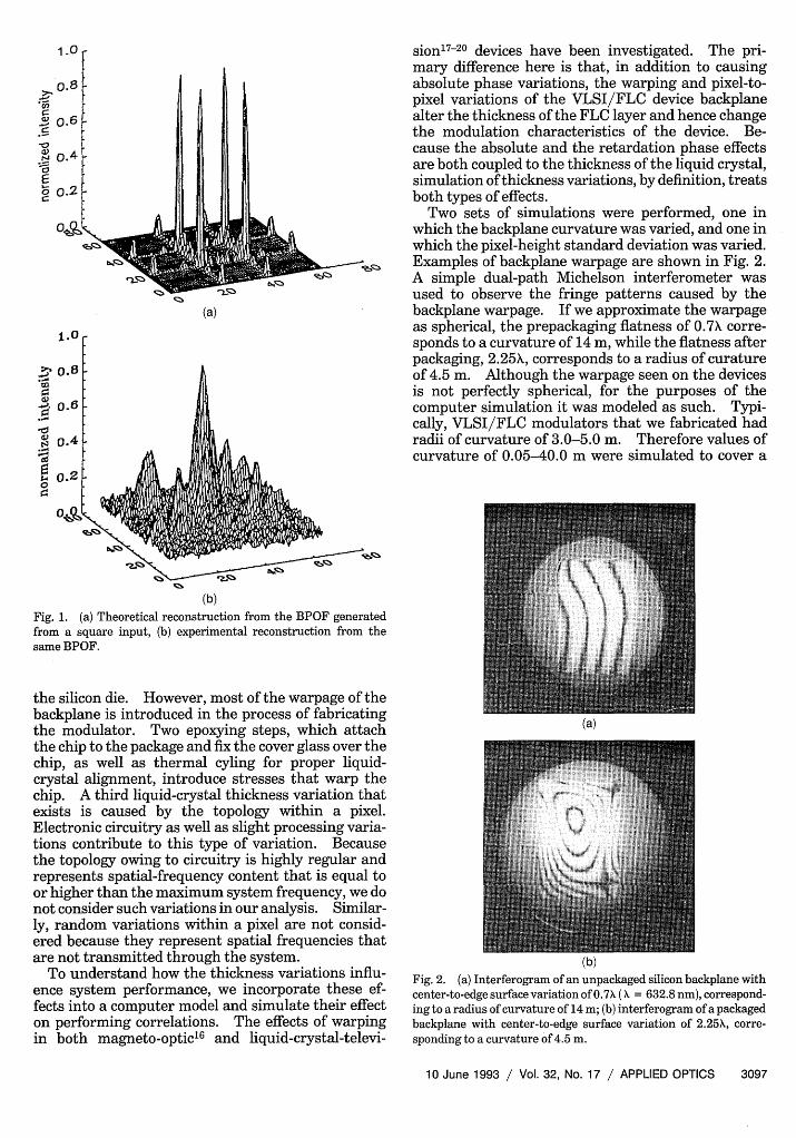
sion17-20 devices have been investigated. The pri-mary difference here is that, in addition to causingabsolute phase variations, the warping and pixel-to-pixel variations of the VLSI/FLC device backplanealter the thickness of the FLC layer and hence changethe modulation characteristics of the device. Be-cause the absolute and the retardation phase effectsare both coupled to the thickness of the liquid crystal,simulation of thickness variations, by definition, treatsboth types of effects.
Two sets of simulations were performed, one inwhich the backplane curvature was varied, and one inwhich the pixel-height standard deviation was varied.Examples of backplane warpage are shown in Fig. 2.A simple dual-path Michelson interferometer wasused to observe the fringe patterns caused by thebackplane warpage. If we approximate the warpageas spherical, the prepackaging flatness of 0.7X corre-sponds to a curvature of 14 m, while the flatness afterpackaging, 2.25X, corresponds to a radius of curatureof 4.5 m. Although the warpage seen on the devicesis not perfectly spherical, for the purposes of thecomputer simulation it was modeled as such. Typi-cally, VLSI/FLC modulators that we fabricated hadradii of curvature of 3.0-5.0 m. Therefore values ofcurvature of 0.05-40.0 m were simulated to cover a
(b)
Fig. 1. (a) Theoretical reconstruction from the BPOF generatedfrom a square input, (b) experimental reconstruction from thesame BPOF.
the silicon die. However, most of the warpage of thebackplane is introduced in the process of fabricatingthe modulator. Two epoxying steps, which attachthe chip to the package and fix the cover glass over thechip, as well as thermal cyling for proper liquid-crystal alignment, introduce stresses that warp thechip. A third liquid-crystal thickness variation thatexists is caused by the topology within a pixel.Electronic circuitry as well as slight processing varia-tions contribute to this type of variation. Becausethe topology owing to circuitry is highly regular andrepresents spatial-frequency content that is equal toor higher than the maximum system frequency, we donot consider such variations in our analysis. Similar-ly, random variations within a pixel are not consid-ered because they represent spatial frequencies thatare not transmitted through the system.
To understand how the thickness variations influ-ence system performance, we incorporate these ef-fects into a computer model and simulate their effecton performing correlations. The effects of warpingin both magneto-optic'6 and liquid-crystal-televi-
(a)
(b)
Fig. 2. (a) Interferogram of an unpackaged silicon backplane withcenter-to-edge surface variation of 0.7 ( = 632.8 nm), correspond-ing to a radius of curvature of 14 m; (b) interferogram of a packagedbackplane with center-to-edge surface variation of 2.25X, corre-sponding to a curvature of 4.5 m.
10 June 1993 / Vol. 32, No. 17 / APPLIED OPTICS 3097
1.0
c-.t5N o.4t= o.
(a)
1.0
.S o.8ul 0.6-1. 0.6
.
10
IV 0.4
k 0.2
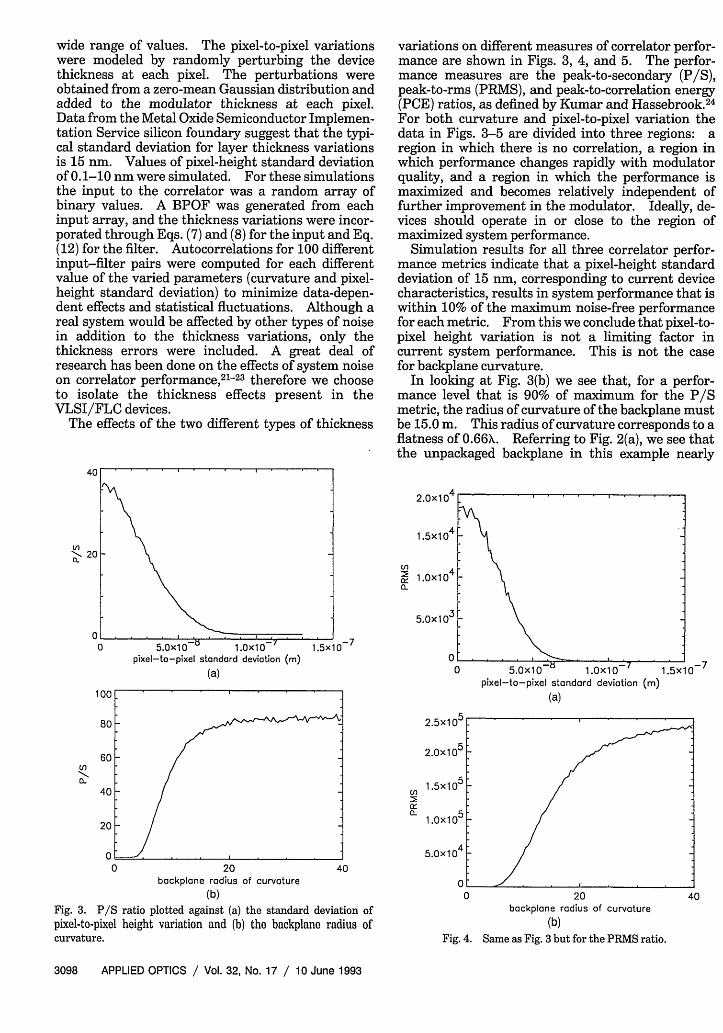
wide range of values. The pixel-to-pixel variationswere modeled by randomly perturbing the devicethickness at each pixel. The perturbations wereobtained from a zero-mean Gaussian distribution andadded to the modulator thickness at each pixel.Data from the Metal Oxide Semiconductor Implemen-tation Service silicon foundary suggest that the typi-cal standard deviation for layer thickness variationsis 15 nm. Values of pixel-height standard deviationof 0.1-10 nm were simulated. For these simulationsthe input to the correlator was a random array ofbinary values. A BPOF was generated from eachinput array, and the thickness variations were incor-porated through Eqs. (7) and (8) for the input and Eq.(12) for the filter. Autocorrelations for 100 differentinput-filter pairs were computed for each differentvalue of the varied parameters (curvature and pixel-height standard deviation) to minimize data-depen-dent effects and statistical fluctuations. Although areal system would be affected by other types of noisein addition to the thickness variations, only thethickness errors were included. A great deal ofresearch has been done on the effects of system noiseon correlator performance,21 -23 therefore we chooseto isolate the thickness effects present in theVLSI/FLC devices.
The effects of the two different types of thickness
40
enX 20
00
variations on different measures of correlator perfor-mance are shown in Figs. 3, 4, and 5. The perfor-mance measures are the peak-to-secondary (P/S),peak-to-rms (PRMS), and peak-to-correlation energy(PCE) ratios, as defined by Kumar and Hassebrook.24
For both curvature and pixel-to-pixel variation thedata in Figs. 3-5 are divided into three regions: aregion in which there is no correlation, a region inwhich performance changes rapidly with modulatorquality, and a region in which the performance ismaximized and becomes relatively independent offurther improvement in the modulator. Ideally, de-vices should operate in or close to the region ofmaximized system performance.
Simulation results for all three correlator perfor-mance metrics indicate that a pixel-height standarddeviation of 15 nm, corresponding to current devicecharacteristics, results in system performance that iswithin 10% of the maximum noise-free performancefor each metric. From this we conclude that pixel-to-pixel height variation is not a limiting factor incurrent system performance. This is not the casefor backplane curvature.
In looking at Fig. 3(b) we see that, for a perfor-mance level that is 90% of maximum for the P/Smetric, the radius of curvature of the backplane mustbe 15.0 m. This radius of curvature corresponds to aflatness of 0.66A. Referring to Fig. 2(a), we see thatthe unpackaged backplane in this example nearly
En20:0-
(a)
enN.Q.
Fig. 3. P/Spixel-to-pixelcurvature.
0 20backplane radius of curvature
(b)
7
pixel-to-pixel standard deviation (m)(a)
2.5x 10⁵
2.Oxl 05
n:2a-
1 .5x105
1.0x 10⁵
5.0x10440
0
ratio plotted against (a) the standard deviation ofheight variation and (b) the backplane radius of
0 20backplane radius of curvature
(b)
40
Fig. 4. Same as Fig. 3 but for the PRMS ratio.
3098 APPLIED OPTICS / Vol. 32, No. 17 / 10 June 1993

1.0
0.8
wi0a-
0.6
0.4
0.2
0.0
pixel-to-pixel standard deviation (m)(a)
0a-
0.ol o_ . , 0 20
backplane radius of curvature(b)
Fig. 5. Same as Fig. 3 but for the PCE ratio.
meets this curvature requirement, which inthat it should be theoretically possible to obtaperformance that is within 9%U ot the maximum.
Figure 4(b) shows that a performance level that is90% of maximum for the PRMS metric would requirea much flatter backplane. The permissible curva-ture is 25.0 m, which corresponds to 0.4AX. Some ofthe unpackaged backplanes we measured met thisstandard of flatness.
Operation with a high PCE, as shown by Fig. 5(b),can be achieved with the most relaxed backplaneflatness requirements. A curvature of 10.0 m, or acorresponding flatness of 1.OX, obtains PCE perfor-mance that is a 90% of maximum. This amount ofcurvature is obtained easily with most unpackagedbackplanes.
For all three metrics, the curvature found in pack-aged devices (typically 3.0-5.0 m) puts system perfor-mance at a level that is less than 10% of maximumperformance. As an example, if we consider a devicecurvature of 4.5 m, as shown by the photograph inFig. 2(b), we find that the simulation results indicateP/S performance of 2.0 (2.5% of maximum), PCEperformance of 4.0 (4.1% of maximum), and negligi-ble PRMS performance. Considering the currentflatness of packaged devices, we conclude that thesimulations predict correlator system performancethat is substantially below maximum owing to thebackplane warpage.
4. Experimental Results
The system diagram of the optical-correlator experi-mental apparatus is shown in Fig. (6). A collimatedinput beam (f/3 collimating lens) from a He-Ne laser(X = 632.8 nm) is reflected by the polarizing beamsplitter and transmitted through a half-wave platethat properly orients the input polarization relativeto the FLC optic axis. Light reflected by SLM1 isencoded with the input pattern and decoded into abinary-amplitude-modulated image by the polarizingbeam splitter. Lens Li (f = 200 nm and D = 50
0_7 mm) performs the Fourier transform of the input,which is multiplied by the filter pattern, encoded as aBPOF on SLM2. Another half-wave plate precedesSLM2 to reorient the polarization for the phase-onlyfiltering operation. The resulting wave front is re-flected by the ordinary beam splitter, and lens L2(f = 150 mm and D = 50 mm) forms the Fouriertransform of the input-filter product at the cameraplane. The y-oriented analyzer removes the un-wanted polarization component [see Section 2, Eqs.(12) and (13)]. The use of the ordinary beam splitterreduces the correlator optical throughput by 75%.Exact control of the liquid-crystal orientation orrotation of the filter-plane device would permit apolarizing beam splitter to be used, eliminating the
40 external polarizer (POL) and increasing the through-put.
The entire experiment is controlled by an IBM-compatible personal computer. Two custom-builtinterface boards drive the SLM's, and the CohuCCD-camera output is stored in the computer byusing a frame grabber.
dicates The input pattern to the system was a circlein P/S (sampled by the array), and filters were generated as
HeNe
Ll
PBSSLM1
SLM2OBS WP2M __
POL
Fig. 6. Optical correlator system using VLSI/FLC SLM's. WP1and WP2 are half-wave plates; PBS and OBS are'polarizing andordinary beam splitters, respectively. Lens Li has a focal lengthof 200 mm, lens L2 a focal length of 150 mm.
10 June 1993 / Vol. 32, No. 17 / APPLIED OPTICS 3099

Fig. 7. VLSI/FLC correlator output: P/S = 1.85, PRMS =16.84, PCE = 3.68%.
discussed in Section 2. Because VLSI/FLC SLM'soperate at frame rates of greater than 2 kHz, thesame input and filter data were written to the devicescontinuously to permit the CCD camera to capturethe correlation data. Data from the camera weredigitized and converted to a surface plot, which isshown in Fig. (7). The performance measures dis-cussed earlier are also indicated in the plot of thedata. The P/S, PRMS, and PCE values are 1.85,16.84, and 3.68%, respectively. Referring back toFigs. 3-5, we see that these values are consistent withthe values predicted by the simulations for the curva-tures that exist in current devices. Specifically, P/Svalues within ± 10% of 1.85 correspond to curvaturesof approximately 3.4-5.0 m, according to Fig. 3(b).Similarly, values of PCE within 10% of 3.68%correspond to curvatures of 3.6-4.5 m, as seen in Fig.5(b). For the PRMS metric the data from the simu-lation cannot be compared reliably with the systemresult. However, it is clear from Fig. 4(b) that thePRMS performance for the real system is below thelevel of simulation-predicted performance for a back-plane with a 5.0-m radius of curvature. All of thevalues for the performance metrics that were ob-tained from the experimental system are slightlylower than those in the simulations, owing to systemnoise inherent in experimentation that is not ac-counted for by the simulation (e.g., Gaussian beamprofile, scattered light, and nonuniform liquid-crystalalignment). The data from the experimental correla-tor support the conclusion arrived at through thesimulations: the curvature of the silicon backplanereduces significantly the system performance, andfabrication techniques need to be improved to reducethe warping of the devices.
5. Conclusions
An optical correlator using VLSI/FLC SLM's at boththe input and filter planes was designed and experi-mentally demonstrated. The input-filter-plane de-vices are capable of frame rates in excess of 2 kHz.Simulation results indicating the relationship be-tween VLSI/FLC modulator characteristics and cor-
relator performance are presented. In particular,the dependence of the performance metrics P/S,PRMS, and PCE on backplane curvature and pixel-to-pixel height variations was determined through thesimulations. The experimental results for this first(to our knowledge) implementation of a VLSI/FLCSLM-based correlator are P/S = 1.85, PRMS =16.84, and PCE = 3.68%. Good agreement betweenthe experimental system performance and the resultspredicted by the simulations indicates that improve-ment in device flatness by a factor of 5 could lead toorder-of-magnitude improvements in correlator per-formance as determined by the P/S, PRMS, and PCEmetrics. Unpackaged backplanes are 0.2X-1.O inflatness and are flat enough to achieve this amount ofimprovement. Current research is directed at elimi-nating the stresses that cause the warping of thebackplane during packaging and device fabrication.This research includes investigations into stress-freeepoxies, solder bump technology, and liquid-crystalalignment techniques. Using reduced-stress ep-oxies, we have packaged silicon test chips that show aflatness of 0.5X, corresponding to a radius of curva-ture of 20.0 m. In the future, VLSI/FLC modula-tors can be fabricated to these flatness specificationsand applied to correlators and other compact optical-processing architectures with improved system perfor-mance.
The authors thank David Doroski for assistance infabricating the VLSI/FLC modulators. This workwas supported by the National Science FoundationEngineering Research Center for Optoelectronic Com-puting Systems, ECD9015128, and by the MartinMarietta Corporation. Graduate fellowship supportfrom NASA, Johnson Space Center, for David Jared isgratefully acknowledged.
References and Notes1. I. Underwood, D. G. Vass, and R. M. Sillitto, "Evaluation of an
nMOS VLSI array for an adaptive liquid-crystal spatial lightmodulator," IEE Proc. 133, 77-82 (1986).
2. D. J. McKnight, D. G. Vass, and R. M. Sillitto, "Developmentof a spatial light modulator: a randomly addressed liquid-crystal-over-nMOS array," Appl. Opt. 28, 4757-4762 (1989).
3. L. K. Cotter, T. J. Drabik, R. J. Dillon, and M. A. Handschy,"Ferroelectric-liquid-crystal/silicon-integrated-circuit spatiallight modulator," Opt. Lett. 15, 291-293 (1990).
4. T. J. Drabik and M. A. Handschy, "Silicon VLSI/ferroelectricliquid crystal technology for micropower optoelectronic comput-ing devices," Appl. Opt. 29, 5220-5223 (1990).
5. D. A. Jared and K. M. Johnson, "Optically addressed threshold-ing very-large-scale-integration liquid crystal spatial lightmodulator," Opt. Lett. 16, 967-969 (1991).
6. D. A. Jared, R. Turner, and K. M. Johnson, "Electricallyaddressed spatial light modulator using a dynamic memory,"Opt. Lett. 16, 1785-1787 (1991).
7. N. A. Clark and S. T. Lagerwall, "Surface-stabilized ferroelec-tric liquid crystal electro-optics: new multistate structuresand device," Ferroelectrics 59, 345-387 (1984).
8. D. Psaltis, E. G. Paek, and S. S. Venkatesh, "Optical imagecorrelation with a binary spatial light modulator," Opt. Eng.23, 698-704 (1984).
3100 APPLIED OPTICS / Vol. 32, No. 17 / 10 June 1993
-§F_1
Ir1�

9. J. L. Horner and P. D. Gianino, "Phase-only matched filtering,"Appl. Opt. 23, 812-816 (1984).
10. J. L. Horner and J. Leger, "Pattern recognition with binaryphase-only filters," Appl. Opt. 24, 609-611 (1985).
11. A. VanderLugt, "Signal detection by complex spatial filtering,"IEEE Trans. Inf. Theory IT-10, 139-145 (1964).
12. D. J. Potter, M. J. Ranshaw, A. 0. Al-Chalabi, N. E. Fancey,
R. M. Stillitto, and D. G. Vass, "Optical correlation using aphase-only liquid crystal over silicon spatial light modulator,"in Optical Information Processing Systems and ArchitecturesIII, Proc. Soc. Photo. Opt. Instrum. Eng., B. Javidi, ed. 1564,363-372 (1991).
13. A. Yariv and P. Yeh, Optical Waves in Crystals (Wiley, NewYork, 1984), Chap. 5, pp. 121-154.
14. SCE 13 is available from British Drug House Limited, BroomRoad, Poole, Bhl2-4NN, England.
15. Chisso 2004 is available from the Chisso Corporation, FineChemicals Division, 2 Kamariya, Kanazawa-ku, Yokahama235, Japan.
16. J. D. Downie, B. P. Hine, and M. B. Reid, "Effects of correctionof magneto-optic spatial light modulator phase errors in anoptical correlator," Appl. Opt. 31, 636-643 (1992).
17. D. P. Casasent and S-F. Xia, "Phase correction of lightmodulators," Opt. Lett. 11, 398-400 (1986).
18. F. Mok, J. Diep, H. K. Liu, and D. Psaltis, "Real-timecomputer-generated hologram by means of liquid-crystal tele-vision spatial light modulator," Opt. Lett. 11, 748-750 (1986).
19. H. M. Kim, J. W. Jeong, M. H. Kang, and S. I. Jeong, "Phasecorrection of a spatial light modulator displaying a binaryphase-only filter," Appl. Opt. 27, 4167-4168 (1988).
20. J. L. Horner, "Is phase correction required in slm-basedoptical correlators?" Appl. Opt. 27, 436-438 (1988).
21. B. Javidi and F. T. S. Yu, "Performance of a noisy phase-onlymatched filter in a broad spectral band optical correlator,"Appl. Opt. 25, 1354-1358 (1986).
22. J. L. Horner and P. D. Gianino, "Signal-dependent phasedistortion in optical correlators," Appl. Opt. 26, 2484-2490(1987).
23. F. M. Dickey, K. T. Stalker, and J. J. Mason, "Bandwidthconsiderations for binary phase-only filters," Appl. Opt. 27,3811-3818 (1988).
24. B. V. K. Vijaya Kumar and L. Hassebrook, "Performancemeasures for correlation filters," Appl. Opt. 29, 2997-3006(1990).
10 June 1993 / Vol. 32, No. 17 / APPLIED OPTICS 3101