Embed Size (px)
Citation preview

Linköping Studies in Science and Technology
Dissertation No. 1492
Optical devices and methods for distributed
lab-on-a-chip analyses
Pakorn Preechaburana
Applied Physics Division
Department of Physics, Chemistry and Biology (IFM)
Linköping University, SE-581 83 Linköping, Sweden
Linköping 2013

Copyright © Pakorn Preechaburana 2013, unless otherwise noted.
All rights reserved.
Optical devices and methods for distributed lab-on-a-chip analyses
ISBN: 978-91-7519-732-6
ISSN: 0345-7524
Printed by LiU-Tryck, Linköping, Sweden 2013

“The mind is everything.
What you think you become.”
(Buddha)


v
Abstract
Lab-on-a-chip (LOC) technologies entail the miniaturization of analytical systems, and the
reduction of required sample and reagent volumes. LOC devices offer compact alternatives to
classical instrumentation while delivering comparable performance and disposable formats.
These aspects make disposable LOC a clear candidate to support distributed chemical sensing
applications; however, the need of accessory services and readout obstructs the
materialization of pervasively distributed LOC solutions.
In this thesis methods and devices to solve this problem are investigated. A distinctive
aspect of this work is the pursuit of solutions based on disposable LOC elements specifically
conceived to exploit ubiquitous infrastructure for readout and evaluation.
Consumer electronic devices, such as cell phones are ubiquitous platforms with residual
capabilities that can be used for chemical sensing, if properly interfaced. This work
investigates elements and tools needed to empower cell phones as readers of disposable LOC
devices and commercial disposable tests.
Access to flexible fabrication of LOC devices at low cost is an important requisite for
testing ideas and implementing customized solutions. A first contribution in this thesis is the
development of a platform for mask less fabrication of 3D microstructures, which coexists on
a routine fluorescence microscope. This microscope projection lithography system (MPLS) is
capable of controlled 3D micro structuring, including cavities and cantilever geometries, and
the sealing of monolithic micro cavities to glass substrates as well as the connection to large
scale service areas. This fabrication platform and other fabrication methods were used along
this thesis to provide disposable optical and fluidic components.
Besides custom-made LOC solutions there are well-established commercial disposable
devices, which are essentially compatible with decentralized diagnosis, except for the use of
specialized readers that confine them to medical centers. The implementation of high
dynamic range (HDR) imaging with standard cell phones, using the phone screen to control
exposure, shows that sensitivity and resolution can be boosted to permit robust evaluation of
this type of disposable tests, in decentralized scenarios.
Solutions employing commercial tests, which have not been designed for cell phone
evaluation, are typically suboptimal and the investigation of customized LOC components
occupies a central role in this thesis. Accordingly, one important aspect to evaluate LOC

vi
devices in compact configurations is to be able to image the LOC at a close distance from the
phone camera, a condition for which phones cameras are not able to focus.
In addition, different phone brands and models have different optical specifications, and a
practical refocusing solution should adapt to all of them. In this work an adaptive lens
concept, complemented by phone time-lapse acquisition, which can be integrated in
disposable LOCs, is demonstrated.
The implementation of sensitive detection methods, such as surface plasmon resonance
(SPR), which is compatible with label free protocols that simplify sample conditioning, is
central to the materialization of ubiquitous LOCs readable with cell phones. In this thesis a
disposable optical coupler, conditioning illumination taken from the phone screen, is used to
create an angle resolved SPR signal from a LOC, which is read with the phone front camera.
Tested performance is comparable with commercial compact SPR modules and detection of
!2 microglobulin, which is an established marker for cancer, inflammatory disorders, and
kidney disease, is within the diagnostics range for blood and urine.
Finally, fluorescence detection within classical LOC devices is tailored to be detectable
with consumer cameras. In this case a disposable optical coupler and fluidics is designed to
condition laser illumination into total internal reflection excitation, while DSLR and phone
cameras capture optically separated fluorescence. The system configuration supports a broad
dynamic range and HDR imaging enables localized resolution boost at selected detection
ranges. Detection of free fucose, a diagnostic marker for liver cirrhosis and several cancer
forms, is shown feasible with a HDR implementation, as one last example of practical LOC
detection schemes for decentralized scenarios.

vii
Populärvetenskaplig sammanfattning
Optiska komponenter och metoder för distribuerad analys med ”lab-on-a-chip”
Lab Denna avhandling visar hur speciellt anpassade ”laboratorier-på-en-bricka” (lab-on-a-
chip, LOC) kan användas för en analys av en rad parametrar, inte minst av intresse för
hälsokontroll. LOC är i sig föremålför en intensiv forskning och utveckling. Avhandlingen
beskriver design, tillverkning och tillämpningar av LOC för engångsbruk dedicerade för att
användas tillsammans med en mobiltelefon, där telefonens kamera och skärm ingår som
komponenter i ett optiskt detektionssystem. Avancerade optiska analyser demonstreras i
avhandlingen med LOCs tillverkade med en metod som inte behöver komplicerade masker
för fotolitografi utan där tredimensionella mikrostrukturer, inkluderande flödeskanaler, byggs
upp genom en programmerad belysningssekvens i ett mikroskop.
I avhandlingen beskrivs också hur en mobiltelefon har använts för kommersiellt tillgängliga
tester baserade på kontrastförändringar. Ett sådant exempel är detektion av en markör för
hjärtsvikt (NT-pro-BNP), där för första gången en mjukvara som tillåter avbildning inom ett
stort dynamiskt exponeringsområde (high dynamic range photography, HDR) används för
sensorändamål för att ge ökad känslighet och upplösning.
Skräddarsydda LOC har använts för att demonstrera mobiltelefonens användning för två av
de viktiga metoderna för analys av biomarkörer. Dessa metoder är fluorescens samt
ytplasmonresonans (SPR). SPR är baserad på ett optiskt fenomen i ett tunt metall (guld) skikt
och har utvecklats till en standardmetod för att analysera bindning mellan biomolekyler, t.ex.
mellan antigener och deras antikroppar. Här kopplas ljuset från mobiltelefonens skärm till en
SPR känslig yta och det reflekterade ljuset analyseras av mobiltelefonens kamera på samma
sida som skärmen. Detta görs med hjälp av en LOC för engångsbruk. Egenskaperna hos
denna uppsättning är jämförbar med kommersiellt tillgängliga kompakta SPR-system.
Detektion av en etablerad markör för cancer, inflammation och njursjukdomar (!2-
mikroglobulin) i blod eller urin inom ett kliniskt intressant område blev den första
tillämpningen.
HDR har används tillsammans med en annan LOC för att detektera fluorescens med hjälp av
mobiltelefonens kamera. LOC ser till att excitation med hjälp av en laser sker genom total
intern reflektion i en mikroflödeskanal och att endast fluorescensen träffar kameran.
Detektion av fukos i urin (markör för bl.a. skrumplever) vid kliniskt relevanta

viii
koncentrationer ges som ett sista praktiskt exempel på resultaten av den forskning som
avhandlingen avser.
Sammanfattningsvis så visas på möjligheten att använda etablerade analytiska metoder för
medicinsk diagnostik med hjälp av engångskomponenter, en mobiltelefon och lämplig
programvara.

ix
Preface
The work presented in this doctoral thesis is a result of my PhD studies between March 2008
and November 2012 at the Optical Devices Laboratory at Department of Physics, Chemistry
and Biology (IFM), Linköping University (LiU). This thesis mainly concerns the methods
and devices for disposable lab-on-a-chip (LOC) devices and optical elements, which are used
to support distributed chemical sensing applications conceived to operate on cell phones. My
main supervisor has been Assoc. Prof. Daniel Filippini and my co-supervisor has been Prof.
Ingemar Lundström. This work has been supported by a PhD scholarship from Thammasat
University (TU) of Thailand and three grants from Linköping Center for Life Science
Technology (LIST). The results are presented in five papers that collect the scientific output
of my work
This thesis is divided in two parts. The first part provides a general introduction to LOC
technologies and describes the background, including microscope photolithography systems
(MPLS), sessile drops lenses, high dynamic range (HDR) imaging, surface plasmon
resonance (SPR) and total internal reflection fluorescence, with their associated applications.
The second part is a collection of the five papers included in this thesis.
Pakorn Preechaburana
Linköping, November 2012

x

xi
List of papers and contributions
Papers included in this thesis
I. Fabrication of monolithic 3D micro-systems
P. Preechaburana, D. Filippini
Lab on a Chip, 2011, 11, 288-295.
(My contribution: optical design, assembly, optimization, microfabrication, characterization
and writing)
II. HDR imaging evaluation of a NT-proBNP test with a mobile phone
P. Preechaburana, S. Macken, A. Suska, D. Filippini
Biosensors and Bioelectronics, 2011, 26, 2107-2111.
(My contribution: part of the experimental work, data analysis and writing)
III. Embedded adaptive optics for ubiquitous lab-on-a-chip readout on intact cell
phones
P. Preechaburana, A. Suska, D. Filippini
Sensors, 2012, 12, 8586-8600.
(My contribution: microfabrication, characterization, sessile drop imaging and writing)
IV. Surface Plasmon resonance chemical sensing on cell phones
P. Preechaburana, M. Collado Gonzalez, A. Suska, D. Filippini
Angewandte Chemie International Edition, 2012, 51, 11585-11588.
(My contribution: optical design, fabrication, assembly and integration, characterization, and
writing)
V. Disposable total internal reflection fluorescence lab-on-a-chip for medical diagnosis
P. Preechaburana, P. Erlandsson, E. Åström, P. Påhlsson, D. Filippini, N. D. Robinson
In manuscript, 2012.
(My contribution: optical design, devices fabrication, optical measurements, HDR data
processing and writing)
xii
Other papers not included in this thesis
VI. Snapshot mask-less fabrication of embedded monolithic SU-8 microstructures with
arbitrary topologies
P. Preechaburana, D. Filippini
Procedia Chemistry, 2009, 1, 778-781.
VII. Mobile phone analysis of NT-proBNP using high dynamic range (HDR) imaging
P. Preechaburana, S. Macken, A. Suska, D. Filippini
Procedia Engineering, 2010, 5, 584-587.
VIII. Fast prototyping of monolithic micro-system on epi-fluorescence microscopes
P. Preechaburana, D. Filippini
Procedia Engineering, 2010, 5, 870-873.

xiii
Conference contributions
Snapshot mask-less fabrication of embedded monolithic SU-8 microstructures with
arbitrary topologies
P. Preechaburana, D. Filippini
Eurosensors XXIII, 6-9 September 2009, Lausanne, Switzerland, Poster.
Mobile phone analysis of NT-proBNP using high dynamic range (HDR) imaging
P. Preechaburana, S. Macken, A. Suska, D. Filippini
Eurosensors XXIV, 5-8 September 2010, Linz, Austria, Oral.
Fast prototyping of monolithic micro-system on epi-fluorescence microscopes
P. Preechaburana, D. Filippini
Eurosensors XXIV, 5-8 September 2010, Linz, Austria, Poster.
3D mask-less photolithography on epi-fluorescence microscopes
P. Preechaburana, D. Filippini
Micronano System Workshop (MSW2010), 4-5 May 2010, Stockholm, Sweden, Poster.
Generic optical coupler for angle-resolved SPR imaging on lap-on-a-chip devices
P. Preechaburana, D. Filippini
Lap-on-a-Chip European Congress, 30 June - 1 July 2011, Hamburg, Germany, Poster.
Adaptive disposable lens for cell phone lab-on-a-chip readout
P. Preechaburana, D. Filippini
Lap-on-a-Chip European Congress, 30 June - 1 July 2011, Hamburg, Germany, Poster.
Cell phone-based surface plasmon resonance imaging for lab-on-a-chip devices
P. Preechaburana, D. Filippini
Micronano System Workshop (MSW2012), 9-10 May 2012, Linköping, Sweden, Poster.

xiv
xv
Acknowledgements
First and foremost, I would like to express my gratitude to Thammasat University of
Thailand for giving me a valuable PhD scholarship which has opened my eyes to the world of
graduate work and research opportunities at Linköping University.
During almost five years of my PhD study, I have had the pleasure to meet and
collaborate with helpful people. Without them, this thesis could not be possible. So I would
like to take this opportunity to express my appreciation to some of them. In particular, I
would like to thank…
Assoc. Prof. Daniel Filippini, my main supervisor, for accepting me as your PhD student
at Optical Devices Laboratory. You have given me invaluable support and supervision
throughout the years. Your room is always opened for our face-to-face discussions which can
help me create new ideas to solve problems in unexpected ways. I am also grateful for your
effort on correcting this thesis. You have guided me not only in the sciencetific research but
also in the world of photography. Thank you for introducing me how to take beautiful photos
and how to create HDR images. I have learned so much from you and I am truly thankful for
everything.
Prof. Ingemar Lundström, my co-supervisor, for your quick and valuable feedback on
reading and correcting this thesis.
Dr. Anke Suska, for your causing laugh in the lab. A cheerful, truly friendly smile makes
you more approachable from others. In addition, thank you for wonderful dinners every time
I have visited. I am definitely glad to meet Malena, your little princess.
Prof. Jens Birch, my mentor, for continuous support during my PhD study.
Acting Prof. Stefan Klintström, head of the Applied Physics Division, for the nice
research environment in this group.

xvi
Co-authors of the papers for invaluable collaboration. It has been a pleasure doing
research with all of you.
Dr. Chun-Xia Du, Jeanette Nilsson and Dr. Stephen Macken for your help. I have
learned a lot from you how to work in cleanroom.
Bo Thunér for invaluable practical assistance in workshop.
Anna Maria Uhlin for your administrative works and for organizing our group meeting.
All Thai friends for so much laugh and great time we have had together.
My teachers and colleagues at Thammasat University, Chulalongkorn University and
Linköping University for your support and help, making it possible for me to realize my PhD
study.
Dao for your love, inspiration, understanding and support. Thank you for always being
beside me.
My parent and family for your endless love and for everything you have done for my
life.

Contents
Abstract . . . . . . . . . . . . . . . . . . . . . . . . . . . . . . . . . . . . . . . . . . . v
Populärvetenskaplig sammanfattning . . . . . . . . . . . . . . . . . . . . . . . . . . . vii
Preface . . . . . . . . . . . . . . . . . . . . . . . . . . . . . . . . . . . . . . . . . . . ix
List of papers and contributions . . . . . . . . . . . . . . . . . . . . . . . . . . . . . . xi
Acknowledgements . . . . . . . . . . . . . . . . . . . . . . . . . . . . . . . . . . . . xv
Part I: An introduction to the field 1 1. Introduction 3
2. Microscope projection lithography system 9
2.1 MPLS design . . . . . . . . . . . . . . . . . . . . . . . . . . . . . . . . . . 11
2.2 Gray-scale photolithography . . . . . . . . . . . . . . . . . . . . . . . . . . 12
2.3 Fabrication of 3D microstructures . . . . . . . . . . . . . . . . . . . . . . . 13
3. High dynamic range imaging 17
3.1 HDR image acquisition . . . . . . . . . . . . . . . . . . . . . . . . . . . . . 18
3.2 Tone mapping . . . . . . . . . . . . . . . . . . . . . . . . . . . . . . . . . . 20
3.3 HDR photography . . . . . . . . . . . . . . . . . . . . . . . . . . . . . . . 20
4. Sessile drops 23
4.1 Contact angle and wetting phenomenon . . . . . . . . . . . . . . . . . . . . 24
4.2 Evaporation of sessile drops . . . . . . . . . . . . . . . . . . . . . . . . . . 25
4.3 Application for optical detection . . . . . . . . . . . . . . . . . . . . . . . . 27
5. Surface plasmon resonance 31
5.1 SPR principle . . . . . . . . . . . . . . . . . . . . . . . . . . . . . . . . . . 31
5.2 Design of coupling optics for SPR sensing on cell phone . . . . . . . . . . . 36
6. Total internal reflection fluorescence 39
6.1 Fluorescence principle . . . . . . . . . . . . . . . . . . . . . . . . . . . . . 39
6.2 Total internal reflection principle . . . . . . . . . . . . . . . . . . . . . . . . 41
6.3 Optical design . . . . . . . . . . . . . . . . . . . . . . . . . . . . . . . . . 44
6.4 Integrated optical setup . . . . . . . . . . . . . . . . . . . . . . . . . . . . . 45
Bibliography 47
Part II: Papers 55


1
Part I
An introduction to the field

2

Chapter 1. Introduction
3
Chapter 1
Introduction
Lab-on-a-chip (LOC) devices are a particular category of micro electro mechanical systems
(MEMs). LOC, also referred to as micro total analysis system (µTAS), miniaturize and
integrate single or multiple laboratory operations in a compact format [1]. LOC technologies
comprising microfluidic systems deal with the handling of fluids using microchannels, which
permit analytical detections with small sample and reagent volumes, and high performance.
Continuous development of the LOC technologies offers other essential benefits including
faster analysis times, better process control and lower manufacturing cost [2-4]. Early demonstration of MEMs can be traced back to the 1960s. Miniaturized pressure
sensors of micrometer and sub-micrometer sized silicon structures were demonstrated by
several groups in the early 1960s, while one of the first µTAS devices was a gas
chromatographic air analyzer developed by S. C. Terry et al. at Stanford university and
published in 1979 [5]. In the late 1980s and early 1990s, numerous microfluidic handling
devices, such as micropumps and flow sensors were developed, and sample conditioning
processes such as mixing and separation steps were integrated in µTAS devices.
In the mid 1990s, µTAS technologies were employed for molecular biology applications
and for military purposes aiming at deployed warfare agent detection. The term lab-on-a-chip
was introduced from this breed of applications, which is not only restricted to analyses
carried out in laboratory facilities.

Chapter 1. Introduction
4
In contrast to more costly silicon MEMs devices, LOC employs alternative materials such
as SU-8 photoresists and polydimethylsiloxane (PDMS), which are cheaper and easier to use
for microstructures fabrication [2, 6]. Microfluidic components such as channels [7-9], valves
[10], pumps [11] and optics [12-14] integrated in LOC devices have been demonstrated in
both SU-8 and PDMS. Especially in the case of optical devices these materials are convenient
since their optical characteristic are similar to glass.
Dedicated microfabrication methods have been developed for LOC devices; however,
they are typically limited to experts and specialized facilities [15]. Conventional
photolithography using chrome binary masks is widely used to fabricate microstructures and
PDMS templates, although this method involves relatively high cost of masks, which
additionally need to be entirely replaced if modifications, addressing improvements in the
design, need to be introduced [16, 17].
Alternatively mask-less photolithography is capable to incorporate changes in the
fabrication process in a more effective way. Several mask-less photolithography methods
such as gray-scale microfluidic photomasks [18], printed color mask [19], binary gray-scale
physical masks [20] and multi photon absorption polymerization [21] have been developed to
fabricate microstructures. One successful technique to produce complex 3D microstructures
is micro-stereo lithography (µSL) [22-24], which utilizes precision 2D scanning of a focusing
light beam over a photo-curable resist, thus building 3D microstructures layer by layer.
A more versatile mask-less instrumentations, the microscope projection lithography
system (MPLS) utilizes liquid crystal displays (LCD) [25, 26] or digital micromirror devices
(DMD) [27, 28] working as spatial light modulators (SLM) for pattern generation, thus
enabling direct conversion of 2D gray-scale layouts to 3D polymer microstructures in just
one exposure step.
In Paper I, a fabrication process implemented as a DMD-based MPLS that overcome
some obstacles including cavity formation, alignment and sealing procedures, which affect
existing methods [29-31], is demonstrated. This system co-exists as a modulated light source
on a Zeiss Axiovert 40 CFL inverted routine microscope, and is able to configure complex
3D microstructures of SU-8 including monolithic cavities, suspended cantilever structures
and sealed microchannels to glass substrates, as well as the connection to service areas. This
fabrication technique and also regular soft-lithography methods for PDMS are used in this
thesis to construct the optical and fluidic components.
Accurate diagnosis is a prerequisite for effective treatments and early detection of
diseases. Diagnosis and health monitoring typically involve time-consuming and costly

Chapter 1. Introduction
5
procedures; with most services centralized in healthcare centers. Alternatively, distributed
diagnosis entailing LOC devices and other technologies have been proposed as a cost-
effective and easy to use alternative [32-36]. In this scenario patients can use these
decentralized tools in absence of sanitary infrastructure and specialists to seek early diagnosis
or routine monitoring by themselves.
One example of this paradigm is based on non-standard LOCs, such as 3D microfluidic
paper analytical devices (µPADs) [37, 38], which are used for point-of-care analysis and
configured for visual readout.
In this thesis conventional LOC devices, fabricated from SU-8 and PDMS, compatible
with high analytical performance, are configured as disposable devices to support distributed
chemical sensing applications that can be accurately evaluated with cell phones. A distinctive
aspect of this thesis is the pursuit of solutions based on disposable LOC elements specifically
conceived to exploit ubiquitous infrastructure for readout and evaluation.
Consumer electronic devices (CEDs), such as scanners [39, 40], web cameras [41, 42]
and cell phones [43, 44] have been demonstrated for readout of chemical sensors. Among the
CEDs, cell phones are ubiquitous platforms with residual capabilities that can be used for
chemical sensing, if properly interfaced. This work investigates elements and tools needed to
empower cell phones as readers of disposable LOC devices and commercial disposable tests.
Heart failure is a serious medical condition that allowedly reduces patient mobility, while
simultaneously requires routine monitoring of health indicators, which typically demands to
attend to health centers for evaluation. Decentralized monitoring of this marker would make
the procedure more comfortable for the patients, contribute to the compliance and adherence
to treatment and help to release medical centers from routine tasks.
The N-terminal proBNP molecule (NT-proBNP) is a cleavage product of the precursor
protein B-type natriuretic peptide (BNP), the concentration of which in blood is a key
predictor of cardiovascular mortality in patients with diagnosed heart failure [45].
In Paper II the evaluation of a disposable commercial sensing test, well-established for
NT-proBNP (Roche Cardiac proBNP), which is essentially compatible with decentralized
use, except for the use of specialized readers, is demonstrated using a regular cell phone.
Since in the present case, the detection consists of quantifying the contrast level of a
region of interest (ROI) on the NT-proBNP test, a high dynamic range (HDR) [46] image
acquisitions procedure was implemented. By using the phone screen for controlled

Chapter 1. Introduction
6
illumination and employing only the most basic resources from Java ME to control image
acquisition, a solution compatible with most mobile phones was achieved.
HDR techniques record an extended dynamic range by composing and tone mapping a
number of images acquired under different exposures [47], and in this case enables
quantitative determinations with a substantial increase in the sensitivity and resolution, which
foster the usability of cell phones for detection.
Disposable LOC devices have been demonstrated for numerous sensing and clinical
applications [48]; however, their dissemination is restricted by the instrumentation required
for readout. LOC solutions for point of care (POC) or other distributed detections [37] are
typically associated with dedicated and specific off-chip readers [2].
Thus, although LOC devices can be disposable and deployable to a large scale, the
availability of readers and their specific characteristics restrict the dissemination of analyses
based on this technology. Therefore, if disposable LOC devices could be evaluated using
generic and common platforms, such as cell phones, the benefits of this technology could be
made ubiquitous.
Solutions employing commercial tests, which have not been designed for cell phone
evaluation, are typically suboptimal and the investigation of customized LOC components
occupies a central role in this thesis. Among the multiple challenges posed by this goal, one
important aspect to evaluate LOC devices in compact configurations is to be able to image
the LOC at a close distance from the phone camera, a distance at which phones cameras
cannot focus.
In Paper III off-chip readout of disposable LOC devices on cell phones is investigated in
a configuration without additional accessories and using adaptive optics that can be integrated
within the LOCs. The device sits on the camera surface, which provides a reliable mechanical
support, and the necessary optical coupling. This PDMS device temporarily sticks on the
camera during evaluation and is disposed afterwards.
Since cell phone cameras cannot focus at such short distances, the LOC entails a
refocusing element that permits to image the micrometric detection area typical in LOC
devices. Simple fixed lenses can be implemented for a particular camera type [50]; however,
since different brands and models have slightly different optical designs, a generic solution to
this problem demands to adapt to all of these conditions with a unified concept. Adaptive
optics is central for autofocusing and can be implemented in different ways [51–54] as

Chapter 1. Introduction
7
dedicated components, but in this work we pursued a solution that could be embedded in
disposable LOC devices, such as a sessile drop [55–57] complemented by data analysis.
The implementation of sensitive detection methods, such as surface plasmon resonance
(SPR), which is compatible with label free protocols that simplify sample conditioning, is
central to the materialization of ubiquitous LOCs readable with cell phones.
In Paper IV angle-resolved surface plasmon resonance (SPR), which is an established
label-free detection method [58], is migrated to cell phones as a disposable interface.
The SPR coupler central to this implementation is compatible with regular lab-on-a-chip
(LOC) technology and gently adheres to the phone screen surface during the measurement; it
couples and conditions the illumination from the screen and directs the SPR image to the
phone camera. After the measurement the device can be detached and disposed of, thereby
leaving the phone intact.
SPR detection is illustrated with a commercial assay for !2 microglobulin (!2M) [59], an
established marker [60, 61] for cancer, inflammatory disorders, and kidney disease, which are
deemed candidates for complementary monitoring in decentralized conditions; moreover SPR
detection is also illustrated with a custom-made chip including embedded calibration, a key
concept in ubiquitous sensing.
Several human diseases, including liver disease and cancer, are characterized by an
increased synthesis and degradation of carbohydrate structures containing the
monosaccharide fucose. As a result, free fucose can be found in the urine of these patients
[62].
Regular tests for free fucose in urine are typically laborious and costly, whereas a simple
test for urinary fucose that can be used bed-side to give clinicians a fast and cheap way to
determine whether further investigation of liver disease or cancer is necessary, would
constitute a valuable resource.
Conditioning the fluorescence detection to the resolution compatible with consumer and
cell phone cameras is a necessary step to make the decentralized instrumentation simple,
affordable and versatile.
In Paper V, fluorescence detection within classical LOC devices is tailored to be
detectable with DSLR and cell phone cameras. In this case a disposable optical coupler and
fluidics is designed to condition laser illumination into total internal reflection excitation,

Chapter 1. Introduction
8
while the phone camera captures optically separated fluorescence. The system configuration
supports a broad dynamic range and HDR imaging enables localized resolution boost at
selected detection ranges. Detection of free fucose, a diagnostic marker for liver cirrhosis and
several cancer forms, is shown feasible with this system.
This and the other results in this thesis constitute evidence that minimally modified or
even intact cell phones can offer an appropriate platform for accurate chemical analyses,
running on conventional disposable LOC technologies or even adapting to existing
commercial tests.
For optimal results, the design of disposable LOC and optical elements, conceived to
operate on cell phones, introduce a key advantage to materialize convincing ubiquitous LOC
diagnosis.

Chapter 2. Microscope projection lithography system
9
Chapter 2
Microscope projection lithography system
Fabrication of complex 3D microstructures is a central aspect to microelectromechanical
systems (MEMS), micro total analysis systems ( ), micro-fluidic devices, miniaturized
sensors, and optical devices [63-66]. Conventional fabrication methods entail binary
photolithographic techniques, which require costly chromium masks and involve time-
consuming multiple step procedures to fabricate complex microstructures [6, 7]. Fig. 2.1
illustrates increasing levels of complexity in 3D microstructures fabrication. Fig. 2.1(a)
corresponds to 3D microstructures without shape control along the height, which can be
fabricated with a 2D binary mask, whereas a structure fully configured in 3D (Fig. 2.1(b))
requires a more sophisticated technique. Finally, the fabrication of sealed 3D controlled
cavities (Fig. 2.1(c)) entails a higher level of sophistication.

Chapter 2. Microscope projection lithography system
10
Figure 2.1 Scheme of 3D microstructures involving increasing fabrication difficulties (a) 3D
structures created with binary masks (b) 3D positive geometries (c) 3D negative geometries
sealed to substrate.
To reduce the running costs and accelerate the process iteration, mask-less
photolithography techniques have been recently developed for exploratory research,
including gray-scale microfluidic photomasks [18], printed color masks [19] and multiphoton
absorption polymerization [21]. One successful mask-less technique to produce complex 3D
microstructures is micro-stereo lithography (!SL), which utilizes 2D scanning of a beam over
a photocurable resist and operates the procedure layer by layer to configure 3D structures
[22-24]. An alternative mask-less instrumentation, the microscope projection lithography
systems (MPLS) utilizes a liquid crystal display (LCD) [25, 26] or a digital micromirror
device (DMD) [27, 28] working as a spatial light modulator (SLM) for a pattern generation
presenting a direct conversion of 2D gray-scale layouts to 3D polymer microstructures.
In this thesis, a DMD-based MPLS is implemented as co-existing element on a routine
fluorescence microscope that enables the fabrication of simple channels (2D), positive 3D
structures and sealed monolithic 3D cavities of arbitrary geometry as well as suspended 3D
structures of any cross section. Concurrently, the MPLS platform is capable of integration at
two-dimensional scales involving few fabrication steps.

Chapter 2. Microscope projection lithography system
11
2.1 MPLS design
The developed MPLS uses a spatial light modulator as virtual gray-scales mask generator
projected at the focal plane of the microscope. In this way a routine epi-fluorescence
microscope is transformed into a micro-fabrication platform with several benefits, such as
complete 3D control of positive and negative geometries as well as the versatility to coexist
with regular microscope uses [16, 28].
Figure 2.2 (a) Schematic of the fabrication setup. Epi-fluorescence routine inverted
microscope used as a mask-less 3D micro-fabrication platform using a DLP projector
providing patterned illumination. (b) Spectral radiance of white illumination from the
projector. Adapted from Paper I by permission of The Royal Society of Chemistry.
The MPLS setup implemented in this thesis (Fig. 2.2(a)) consists of an inverted routine
microscope (Zeiss Axiovert 40 CFL), a digital light processing (DLP) projector (Optoma
EP1690) with 2500 ANSI lumens and contrast ratios of 2500:1, and a camera prime lens
(Nikkor 50mm f/1.8). Every component can be reassembled in their original configurations
since there are no permanent modifications to the setup. This system exploits the commercial
projector, which comes with an DMD array serving as the virtual photo mask
generator. The high image contrast ratios of DMD-based projectors are well suited with the
lithographic system to generate effective and well allocated exposure [28].
The UV filter glass placed in front of the ultrahigh pressure lamp, which is the light
source of the projector, was removed to increase intensity in the near UV region. The
projector was aligned with the fluorescence illumination path, through the prime lens fixed at
its maximum aperture.

Chapter 2. Microscope projection lithography system
12
Fig. 2.2 (b) illustrates the spectral radiance of the light source measured at the microscope
stage through the glass slide. Regular negative tone photoresist (SU-8) is sensitive to the
broadband near UV radiation in the range of 350 - 400 nm, with a recommended 365 nm (i-
line) [67]. In this setup, a substantial part of the UV light is useful at absorbed by the
projector which is designed for the visible range. The intensity of i-line is very low (0.4
mW/cm2), but still enough to be useful at acceptable long exposures.
Photoresist to become microstructures is spin coated on one side of a glass slide (Menzel-
Glaser) and placed on the microscope XY traverser during the fabrication process. Filter
cubes (Zeiss FT510 in a SET15 filter cube) in the microscope filter block slider are
customized for observation and exposure. During the focusing and alignment process, a green
excitation filter (Zeiss BP 546/12) is mounted in one filter cube to avoid the exposure of the
photoresist. The different focal planes, which can be chosen at the photoresist/air interface
and at photoresist/glass interface, are manually selected using the microscope focusing screw.
If the pattern observed through the eyepiece is perfectly focused in green light, it may be
blurred in near UV because of an axial (longitudinal) chromatic aberration [28, 68]. This
aberration can be corrected by finely adjusting the position between the camera lens and the
projector [28].
Once perfectly focused without the aberration, the sample is exposed by switching to the
next filter cube, which has the excitation filter removed.
Different resolutions and working areas can be achieved by switching objectives. For a
objective the resolution is 30 !m with a working area of ~50mm2, whereas a 10"
objective handles a working area of ~4mm2 with the resolution of 5 !m.
2.2 Gray-scale photolithography
In order to contextualize the contribution of MPLS, alternative procedures are described in
this section. Conventional photolithography (Fig. 2.3(a)) uses binary chrome masks
selectively blocking UV light to generate 2D layouts of a given height [69]. In order to create
3D microstructures, multi-layer photoresist with several masks and multiple exposure steps
are required [70].
Alternatively, gray-scale lithography creates precisely controlled 3D surfaces in a one
step exposure procedure. This technique uses the same protocol for resist preparation i.e. film
coating, soft baking and development process as in the conventional lithography, but the
resist is exposed by a modulated single exposure dose. A low exposure dose cross link, a

Chapter 2. Microscope projection lithography system
13
resist at a shorter depth than a region receiving a high exposure dose. After development, the
resist is dissolved in the proportion of the exposure, thus generating a 3D topology [69, 71] as
illustrated in Fig. 2.3 (b).
Figure 2.3 Comparison of photolithographic techniques (a) conventional binary mask
photolithography and (b) gray-scale photolithography.
An important feature of gray-scale lithography is the number of gray levels which the
system can generate. The spatial light modulator created by the projector used in our MPLS
provides 8 bits resolution. However, the photoresist absorption is nonlinear, and the full
dynamic range of 256 gray-levels can neither be achieved. Accordingly, illuminating patterns
must be calibrated to compensate nonlinearity and range [72].
2.3 Fabrication of 3D microstructures
SU-8 has very low optical absorption (high transparency) above 360 nm, which contributes to
its conventional use to fabricate nearly vertical sidewall structures in thick resist films [73].
However, this makes the precise control of exposure depth in the SU-8 difficult to archive
and embedded channels or suspended structures cannot be fabricated with the light source
used in this thesis.
To address this issue, the properties of the SU-8 are modified by adding a light absorber
in the available spectral range [74, 75].

Chapter 2. Microscope projection lithography system
14
Figure 2.4 Spectral radiance of the light source measured on the microscope stage through a
glass slid, through 30 !m of SU-8 on glass and through 30 !m of SU-8/S1818 on glass.
Adapted from Paper I by permission of The Royal Society of Chemistry.
In this thesis, the SU-8 is mixed with 10% volume of the positive photoresist S1818. The
fabrication process for the mixture (SU-8/S1818) is the same as pure SU-8 and the behavior
of the mixture is like that of SU-8. Unexposed structures are removed upon development and
the increased absorbance in the region of 400-450 nm (Fig. 2.4) provides the required control
of adsorption depth for the available source. Thus complex 3D monolithic suspended
microstructures such as the cantilevers and sealed negative controlled geometries, i.e. vaulted
channels, can be fabricated as illustrated in Fig. 2.5.

Chapter 2. Microscope projection lithography system
15
Figure 2.5 3D images of monolithic microstructures (a) vaulted channels sealed to a glass
substrate and aligned with a positive plano-convex lens. (b) Cantilevers of arbitrary cross
sections. Adapted from Paper I by permission of The Royal Society of Chemistry.

Chapter 2. Microscope projection lithography system
16

Chapter 3. High dynamic range imaging
17
Chapter 3
High dynamic range imaging
Real world scenery can exhibit extreme dynamic ranges, which refers to the differences
between the brightest and the darkest level of light, than that can be captured by existing
recording media. Loss of information in dark and saturated areas is a consequence of this
limited dynamic range recording. On the other hand, the details in bright areas of the scene
can be captured using short exposure times, whereas the details in dark areas can be recorded
for long exposure times [76].
High dynamic range (HDR) imaging is a photographic technique that enables capturing
the complete contrast range of the real scenes. Concurrently, displaying media such as
computer screens and printouts support even shorter dynamic ranges than recording media.
The nonlinear projection of HDR images into these low dynamic range (LDR) media, known
as tone mapping, permits realistic rendering despite the contrast limitations.

Chapter 3. High dynamic range imaging
18
3.1 HDR image acquisition
To acquire HDR images, a multi-exposure method is used in this work. A sequence of images
taken with different exposure times is reconstructed in a post processing stage to generate a
HDR image [77] (Fig. 3.1).
Figure 3.1 A scheme exposure bracketing to acquire a HDR image. A sequence of regular
images is taken with different exposure times and is combined to generate a HDR data set.
The sequence of images of the same scene is captured using a common configuration, in
which the camera aperture (N) is fixed in order to maintain the depth of field constant, and
the exposure time (!) is varied (Fig. 3.2). These parameters are related to the exposure value
EV by:
!
EV = log2N2
"
#
$ %
&
' ( (3.1)
The dynamic range is described in terms of EV difference (
!
"EV ) between the brightest
and darkest areas of the images. This EV difference is related to the contrast ratio, C, by:
!
C = 2"EV (3.2)
Thus a regular reflex camera capable of 11 stops dynamic range (
!
"EV =11) can acquire a
contrast of 1:2048, while real scenes can be in excess of 1:100000.

Chapter 3. High dynamic range imaging
19
Figure 3.2 A series of LDR images of the same scene taken with difference exposure values
(EV =-2, 0, +2).
Figure 3.3 HDR image reconstructed from a series of LDR images in Fig. 3.2 using
PhtomatixPro 3.2.7. The image was tone mapped in tone enhancer.

Chapter 3. High dynamic range imaging
20
3.2 Tone mapping
The dynamic range in HDR images exceeds the capabilities of displaying devices, which
have lower dynamic range. Hence, these displaying media devices cannot render the
complete range of captured light. An image reproduction technique i.e. tone mapping is
required for the purpose to project the information into the LDR range [78], while the details
of the HDR image including the localized contrast between neighboring pixels are
maintained. Thus, fine details in the resulting image are enhanced in dark and bright areas as
shown in Fig. 3.3.
Specific implementations of tone mapping depend on the applications. In some cases, the
target of tone mapping is to maintain a brightness match between HDR scene and the tone
mapped result, while other situations can emphasize as much of fine details in image as
possible. The nature of HDR/tone mapping technique is the flexibility to decide in the post
processing which aspect to highlight.
3.3 HDR photography
The idea of using several exposures was firstly developed by Gustave Le Gray in 1850 [79].
Le Gray attempted to render seascapes showing the strong contrast between the sky and the
sea, which was at that time using standard photography. He made it possible using two
negatives: one exposed for the sky and another one longer exposed for the sea, and then
combined them to create a single photographic print.
In the 1940s, Charles Wyckoff developed wide dynamic range film (XR film) which was
composed of three layers with different sensitivity to light. This film was used to capture
historic images of the first nuclear explosions.
In 1993, Steve Mann introduced a method to generate HDR images from digital multi-
exposure bracketing.
The concept of tone mapping is even older than HDR, and can be observed in attempts of
extending contrast by combining indigo with gold leaf contrast in paints from Cimabve
(1240-1302). Remarkably, 19th
century impressionists highlighted the focus of theses artists
on capturing the light on the canvas by dismissing the accurate rendering of the figures.
Today established software packages, such as Photomatix [80] and Photoshop [81],
combine the capabilities of multi exposure merging and tone mapping in a single
environment.

Chapter 3. High dynamic range imaging
21
Scientific uses of HDR imaging include ultra-high contrast amplification in bright field
microscopy of low contrast phase-object, such as unstained cells and micro-organisms [82].
In this thesis, HDR processing is used to improve sensitivity and resolution in the evaluation
of commercial NT-proBNP tests using standard cell phones.

Chapter 3. High dynamic range imaging
22

Chapter 4. Sessile drops
23
Chapter 4
Sessile drops
A sessile drop is a drop of liquid deposited on a horizontal solid substrate where the wetted
area is confined by a three-phase contact line. The drop geometry is defined by drop height,
contact radius and contact angle. It is found that the contact angle plays an important role in
characterizing surface properties of solid substrate [83, 84] such as the surface energy in
contact angle measurements.
Figure 4.1 The equilibrium of a liquid drop on solid substrate, and acting surface tensions.

Chapter 4. Sessile drops
24
4.1 Contact angle and wetting phenomenon
Fig. 4.1 shows a liquid drop deposited on a solid surface. In equilibrium, the drop is balanced
by three forces acting along the three interfaces between the solid, liquid and vapor phase.
These three forces are the surface tensions between solid and liquid (!SL), between solid and
vapor (!SV), and between liquid and vapor (!LV). The contact angle (") is defined as the angle
formed between the solid/liquid interface and the liquid/vapor interface or alternately
described as the angle between the solid surface and the tangent plane to the surface of liquid.
The contact angle is related to the interfacial tensions by the Young equation [85, 86]:
!
"SV
= "SL
+ "LVcos# (4.1)
Wetting of solid substrates by liquid is a surface phenomenon, which results from the
difference in the surface tensions between the solid and liquid. The degree of wetting
(wettability) can be characterized by measuring the contact angle [87].
If the contact angle is greater than 90º, the solid surface is considered hydrophobic, which
indicates a low surface energy and corresponds to a low degree of wetting. Hydrophilic
surfaces on the other hand correspond to high surface energy and wettability, whereas contact
angles are lower than 90º [87-89]. Fig. 4.2 illustrates the comparison between the
hydrophobic and hydrophilic surfaces. Completely wetting and a completely non-wetting
conditions occur at the extremes of "=0º and "=180º, respectively.
Figure 4.2 Comparison of the hydrophobic and hydrophilic surface specified by the contact
angle.

Chapter 4. Sessile drops
25
4.2 Evaporation of sessile drops
The evaporation of a sessile drop involves simultaneous heat and mass transfer processes,
including conductive heat transfer to the substrate, convective heat transfer, which is affected
by the surface tension, and temperature gradients inside the drop [55]. The sessile drop can be
described as a spherical cap shape when the drop is smaller than the capillary length (~2.7
mm for water), for which the surface tension has more effect than the gravity [90-92]. The
contact angle (!), the contact radius (r), the drop height (h) and the radius of curvature (R) are
used to characterize the spherical cap geometry as shown in Fig. 4.3.
Figure 4.3 Cross section of the spherical cap shape of a small sessile drop. The contact
angle (!), the contact radius (r), the drop height (h) and the radius of curvature (R) are used
to characterize the spherical cap shape.

Chapter 4. Sessile drops
26
Each of these parameters can be written in the function of other two parameters by
considering the geometry as [55]:
!
R =r
sin" (4.2)
!
h =R
1" cos# (4.3)
!
" = 2tan#1 h
r
$
% & '
( ) (4.4)
The volume (V), the drop cap surface area (A), and the radius of curvature (R) can be
expressed in terms of r and h:
!
V ="h(3r2 + h
2)
6 (4.5)
!
A = " (r2 + h2) (4.6)
!
R =r2
+ h2
2h (4.7)
There are three possible modes of evaporation: the constant contact angle mode, the
constant contact radius mode and the mixed mode [92] as shown in Fig. 4.4. During
evaporation in the constant angle mode (Fig. 4.4(a)), the contact angle remains constant and
the drop shape is also unchanged, whereas the contact radius is continuously reduced until the
end of the evaporation. The constant contact radius mode (Fig. 4.4 (b)) is characterized by a
constant contact radius, whereas the contact angle decreases while the evaporation takes
place. For the mixed mode of evaporation (Fig. 4.4 (c)), the contact angle and the contact
radius are altered through the whole evaporation process.

Chapter 4. Sessile drops
27
Figure 4.4 Comparison of liquid evaporation modes: (a) constant contact angle mode (b)
constant contact radius mode and (c) mixed mode.
4.3 Application for optical detection
In this work, sessile drop evaporation is used as a disposable morphing lens for off-chip
readout of LOC devices on any cell phone. Fig. 4.5 illustrates an integrated adaptive focusing
element using a water lens for imaging microscopic detection regions of lab-on-a-chip (LOC)
devices in contact with cell phone cameras. The proposed concept demonstrates a simple and
generic device for optical detection, which can operate across brands and models of intact
cell phones.

Chapter 4. Sessile drops
28
Figure 4.5 (a) Design of the morphing lens. The forward distance (dF) and the back focal
length (BFL) are the parameters setting the lens magnification and describing the adaptive
focusing capabilities. (b) PDMS used for the substrate of the lens, which is attached to the
rear cell phone camera of a Nokia 6720. (C) 3D scheme of the measuring device.
Reproduced from Paper III under the open access license.
The lens is a drop of distilled water delivered from a 0.5 mm needle on a 150 µm thick
PDMS substrate, which mildly adheres to camera surface providing the reliable optical
coupling between these elements.
The PDMS substrate is separated from the LOC devices by a forward distance (dF) less
than 2 mm providing a compact configuration. During the measurement the device
temporarily sticks on the camera and is easily disposed after the measurement leaving the
camera intact.

Chapter 4. Sessile drops
29
Figure 4.6 Collection of sessile drop images captured with a stereomicroscope at a 15 s
interval. The evaporation regimes (indicated as 1, 2 and 3) are highlighted. Reproduced from
Paper III under the open access license.
The evaporation of a water drop from a PDMS substrate measured at 15 s interval at room
temperature shows the three regimes of evaporation (Fig. 4.6). For about half of the recorded
time, the constant contact angle is observed in the first regime (1 in Fig. 4.6) with the changes
of the drop curvature by reducing the contact radius and the height of drop. Mixed mode
occurs in the second regime (2 in Fig. 4.6), the contact radius and the height keep changing,
whereas the contact angle changes accelerate. In the final regime (3 in Fig. 4.6), the constant
contact radius mode is observed, with shape changes accelerating even further, with the drop
pinned at the substrate. In this conditions, a large range of increasing R (and correlated BFLs)
result in the conditions exploited to adapt LOC focusing on diverse phone cameras.

Chapter 4. Sessile drops
30

Chapter 5. Surface plasmon resonance
31
Chapter 5
Surface plasmon resonance
Surface plasmon resonance (SPR) is an optical phenomenon that can be used as a sensing
tool to accurately examine refractive index changes in the very near vicinity of a metal
surface. Common applications of SPR include biomolecular interactions analysis, for which
SPR is a sensitive and label-free method [93-95].
5.1 SPR principle
Surface plasmons (SP) are transverse magnetic (TM) waves which travel along the interface
between a dielectric material and a highly conductive metal, and exponentially decay in the
perpendicular direction to the interface [96, 97]. Surface plasmons arise from a collective
oscillation of free electrons at a metal surface [98, 99] (Fig. 5.1) which in the case of gold
films can be excited at visible frequencies. SPR is the resonant excitation of a surface
plasmon wave along the dielectric-metal interface [100, 101]. This resonance occurs from the
interaction between excitation light and free electrons in the metal only under appropriate
conditions.

Chapter 5. Surface plasmon resonance
32
Figure 5.1 Schematic illustration of the charge distribution and electric field E of a surface
plasmon at a metal/dielectric interface.
Excitation of SP by light
The wave vector,
!
kSP, of the surface plasmon traveling along the metal/dielectric interface
can be expressed as [100]:
!
kSP
="
c
#m#d
#m
+ #d
(5.1)
where
!
" /c is the wavevector of light in vacuum,
!
"m
and
!
"dare respectively the dielectric
permittivity of metal and dielectric medium.

Chapter 5. Surface plasmon resonance
33
Figure 5.2 Dispersion relations of surface plasmons at a metal/dielectric interface
comparing to a light in the dielectric medium and in a glass prism.
Fig. 5.2 shows the dispersion relation of the surface plasmon curve in relation with those
of light traveling in the dielectric medium and in a prism. For the dielectric medium [102,
103]:
!
kd
="
c#d
(5.2)
Accordingly, the surface plasmons cannot be excited in the dielectric medium by directly
shinning light on the metallic surface [103], hence a coupling mechanism is necessary to
match the wavevector; a prism with high dielectric constant (Fig. 5.2) is utilized to couple the
excitation to the surface plasmons [102].

Chapter 5. Surface plasmon resonance
34
Figure 5.3 Schematic arrangement of Kretschmann configuration of a three-layered SPR
system.
Fig. 5.3 illustrates the Kretschmann prism coupling geometry which is the most widely
used technique to attain the SPR phenomenon. The base of the prism is coated with a thin
metal film of approximately 50 nm thick [104], which is kept in direct contact to the
dielectric sample of lower refractive index. Gold is the most common metal used in SPR
sensors because of its stability and relative chemical inertness [105]. P-polarized light is
directed through one side of the prism at an incidence angle greater than the critical angle at
the prism/dielectric interface. Total internal reflection creates an evanescent wave, which in-
plane component of wavevector (
!
kp ) is given by [100, 102]:
!
kp ="
c#p sin$ (5.3)
where
!
"p is the dielectric constant of the prism. When the propagating constant of the
evanescent wave matches that of the surface plasmons at a certain incident angle, which is
called SPR angle (
!
"SPR
), the excitation of surface plasmon occurs [102] with the resonance
condition given by:
!
"
c#p sin$SPR =
"
c
#m#d
#m + #d (5.4)

Chapter 5. Surface plasmon resonance
35
If the reflected light is measured as a function of incidence angle
!
", then a sharp dip at
!
"SPR
is
observed as the conversion of energy to the surface plasmons occurs (Fig. 5.4).
Figure 5.4 A typical SPR spectrum showing the dip at the resonant angle .
Penetration depth
The penetration depth of surface plasmons into the sensing medium is defined as the distance
in the perpendicular direction to the interface at which the intensity of the electric field
decays to 1/e, which is given by [98]:
!
"SPR
=#
2$
% & m
+ &d
&d
2 (5.5)
where
!
" # m
represents the real part of the dielectric constant of metal. For example, if incident
light with = 633 nm is excited on gold film with
!
"m
= #11.6 +1.2i, then the penetration
depth
!
"SPR
= 328 nm into air medium and 177 nm into water medium [103].

Chapter 5. Surface plasmon resonance
36
5.2 Design of coupling optics for SPR sensing on cell phone
Since cell phone displays in current models provide wide-angle illumination with intensities
typically between 300 and 500 nits (equivalent to 43.9 and 73.2
!
µW cm2sr at 555 nm), they
suffice to illuminate angle-resolved SPR experiments. Additionally, modern front cell phone
cameras are typically of VGA resolution which is sufficient to capture angle-resolved SPR
images, with good accuracy.
The coupler used in this work is a disposable optical element made of an optical grade
epoxy (EPO-TEK 301-1, n 1.5) and polydimethylsiloxane (PDMS, n 1.4). In order to
capture the SPR dip for a gold/water interface under red illumination, the epoxy with
matching refractive index to the glass slide (n 1.5) is needed to achieve the necessary
illuminating angles. The glass slide coated by 45 nm of thermally evaporated gold is attached
to the epoxy surface using immersion oil. Simple fluidics or more advanced lab-on-a-chip
(LOC) devices on the surface can be utilized for sample conditioning.
The light source is provided by an image displayed (a red rectangle in this case) in the
cell phone screen, and a white frame is used for the optical coupler placement as shown in
Fig. 5.5(a). The screen illumination is collected by PDMS plano-cylindric element and
conveyed to an 8 mm long region on the gold surface. The angle-resolved SPR signal
reflected from the gold interface is collected by a PDMS cylindrical element and deflected
towards the camera by total internal reflection in a PDMS prism as shown in the ray-tracing
(Fig. 5.5(b)).

Chapter 5. Surface plasmon resonance
37
Figure 5.5 (a) 3D scheme of the setup for angle-resolved SPR optically coupled by a
disposable device with screen illumination and front camera detection (b) 2D ray-trace of the
coupler element showing the light path from screen to camera. Adapted from Paper IV with
permission from Wiley-VCH.

Chapter 5. Surface plasmon resonance
38

Chapter 6. Total internal reflection fluorescence
39
Chapter 6
Total internal reflection fluorescence
Total internal reflection fluorescence (TIRF) exploits an evanescent wave to excite
fluorophores in the limited region adjacent to the interface of two optical media, such as a
glass substrate and a liquid sample [106-110]. Fluorophores in the bulk of the sample are thus
not excited because the evanescent field is extinguished away from the interface. Thus TIRF
provides a powerful technique to selectively excite a functionalized surface and to optically
separate fluorescence from excitation in compact geometries, which can be convenient for
optical chemical sensing [111-114].
6.1 Fluorescence principle
The fluorescence process is illustrated in the Jablonski diagram shown in Fig. 6.1. A
fluorescent substance, i.e. a fluorophore absorbs light and an electron is raised from a ground
state ( ) to an exited state ( ) by absorbing the photon energy.
The excited electron loses part of its energy by dissipation of non-radiative energy to the
surrounding environment and then relaxes to the lowest excited state . This phenomenon is
called internal conversion. From this excited state , the electron will return to the ground
state and simultaneously emit the fluorescent light with a longer wavelength than that of
the exciting photon.

Chapter 6. Total internal reflection fluorescence
40
Figure 6.1 Simplified Jablonski diagram. The diagram illustrates the electronic transition
used to describe the phenomenon of fluorescence.
The Stokes shift is the difference in wavelength of the peak between excitation and
fluorescent emission spectra. The excitation energy
!
Eex
is given by:
!
Eex
= hc /"ex
(6.1)
and emission energy
!
Eem
is given by:
!
Eem
= hc /"em
(6.2)
where
!
"ex
,
!
"em
is the wavelength of the excitation and emission spectra peaks respectively.

Chapter 6. Total internal reflection fluorescence
41
Figure 6.2 Stokes shift between the absorption and emission spectra of maxima.
Due to energy lost in the internal conversion, the emission energy is smaller than the
absorption energy i.e.
!
Eem
< Eex
. The emission spectrum maximum is shifted to longer
wavelength (
!
"em
> "ex
) compared to the excitation spectrum which is illustrated in Fig. 6.2.
6.2 Total internal reflection principle
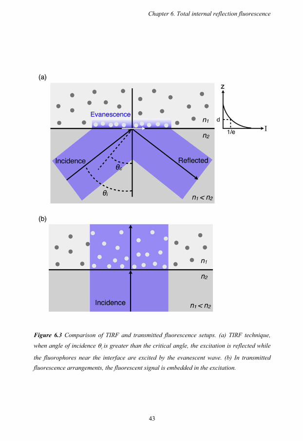
Total internal reflection (TIR) can occur when light propagates from an optical medium of
larger refractive index to a medium of smaller refractive index. Fig. 6.3(a) illustrates how
light behaves at an interface of two medium with different refractive indexes. A beam of light
traveling in the higher refractive index medium i.e. glass (
!
n2"1.51) reaches a medium of
lower refractive index i.e. aqueous solution (
!
n1"1.33#1.38 [116]). For illuminating angles
smaller than the critical angle given by the Snell’s law:
!
"c
= sin#1(n1 /n2), (6.3)
the light beam is refracted in the second medium. If the angle of incidence is greater than
total internal reflection occurs, and the light beam is reflected back within the glass.
Nevertheless, some of the energy of the light beam penetrates through the interface
generating an evanescent electromagnetic wave, which can excite the fluorophores adjacent
to the interface.
Chapter 6. Total internal reflection fluorescence
42
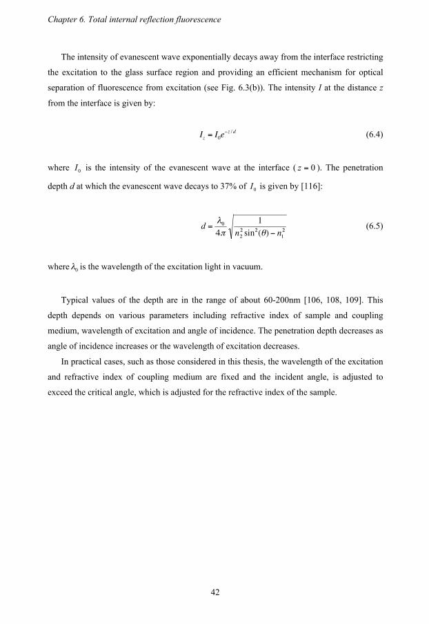
The intensity of evanescent wave exponentially decays away from the interface restricting
the excitation to the glass surface region and providing an efficient mechanism for optical
separation of fluorescence from excitation (see Fig. 6.3(b)). The intensity I at the distance z
from the interface is given by:
!
Iz
= I0e"z / d (6.4)
where is the intensity of the evanescent wave at the interface ( ). The penetration
depth d at which the evanescent wave decays to 37% of is given by [116]:
(6.5)
where is the wavelength of the excitation light in vacuum.
Typical values of the depth are in the range of about 60-200nm [106, 108, 109]. This
depth depends on various parameters including refractive index of sample and coupling
medium, wavelength of excitation and angle of incidence. The penetration depth decreases as
angle of incidence increases or the wavelength of excitation decreases.
In practical cases, such as those considered in this thesis, the wavelength of the excitation
and refractive index of coupling medium are fixed and the incident angle, is adjusted to
exceed the critical angle, which is adjusted for the refractive index of the sample.
Chapter 6. Total internal reflection fluorescence
43
Figure 6.3 Comparison of TIRF and transmitted fluorescence setups. (a) TIRF technique,
when angle of incidence is greater than the critical angle, the excitation is reflected while
the fluorophores near the interface are excited by the evanescent wave. (b) In transmitted
fluorescence arrangements, the fluorescent signal is embedded in the excitation.

Chapter 6. Total internal reflection fluorescence
44
6.3 Optical design
There are diverse configurations to convey the excitation to the sample, in some cases using
an objective lens [117-119] and in others optical coupler such as a prism [120-122]. The latter
has several benefits such as inexpensive setup, greater range of incident angles and a compact
geometry that can be adapted to disposable devices such as the planar waveguide associated
to this thesis. Fig. 6.4 illustrates the cross section of the TIRF excitation. The illuminating
laser beam is refracted by the prism and propagates further along the planar waveguide. In
order to configure a disposable version of this geometry, the prism was fabricated in PDMS
rubber and out of the shelf glass slides constituted the planar waveguide. Concurrently the
PDMS element inherently provides the necessary adhesion to the glass surface required for a
proper mechanical and optical matching, without additional processes. If is larger than
TIR occurs and the illuminating beam propagates in a zigzag path confined to glass slide,
whereas the evanescent wave, which decays exponentially from the interface, selectively
excites the fluorophores in this region.
Figure 6.4 2D cross section of the prism-based TIRF coupler.
The relation among is obtained from the geometry of the assembly as:
(6.6)
The other two relations are deduced from the considering the Snell’s law at the air/prism
interface
!
n0sin"
0= np sin# (6.7)
where , and

Chapter 6. Total internal reflection fluorescence
45
!
" = sin#1 sin$0
np
%
& ' '
(
) * * (6.8)
However, can be expressed in term of by substituting Eqn. 6.8 in Eqn. 6.7. So that:
!
"1
=# + sin$1 sin"0
np
%
& ' '
(
) * * (6.9)
Considering the Snell’s law again at prism/coupling interface:
!
sin"2
=np
nmsin"
1 (6.10)
Hence,
!
"2
= sin#1 np
nmsin"
1
$
% &
'
( ) (6.11)
6.4 Integrated optical setup
Fig. 6.5 shows the implementation of the TIRF setup used in this thesis. The microscope
glass slide (Menzel-Glaser) with
!
nm
=1.51 and 45° PDMS (Dow Corning Sylgard 184) prism
with
!
np =1.4 constitute the excitation coupler. Since the refractive index of the aqueous
samples ( ) considered in this thesis are about 1.33, the angle of incidence at glass
slide/sample interface needs to be larger than 61.7°, the minimum critical angle.
Accordingly, the incidence angle in Fig. 6.5(a) needs to be above 40°.
A blue laser at 473 nm illuminates the PDMS prism as indicated in Fig. 6.5(a), confining
a 3 mm wide beam within the glass slide and exciting fluorophores at the glass surface.
Emitted fluorescence light is captured across the glass slide by a DSLR camera (Canon EOS
500D) and a cell phone camera (iPod touch 4th
generation). An emission filter (Zeiss BP 515-
565) is inserted in front of the camera to remove the scattered excitation in the PDMS fluidic.
In the present case optimum HDR collection is not required and matching of fluorescence in
the iPod camera dynamic range is accomplished by direct imaging of the glass surface. Fig.
6.5(d) shows fluorescence proportional to fucose concentration for a sample in a 100 !m
wide channel as captured by the iPod camera.

Chapter 6. Total internal reflection fluorescence
46
Figure 6.5 The experimental arrangement used for TIRF measurements. (a) Cross section of
the setup. (b) 3D scheme of the experimental assembly. (c) The picture of the actual setup. (d)
The picture of fucose modulated fluorescence light measured with a phone camera.

Bibliography
47
Bibliography
[1] Y. H. Ghallab, Lab-on-a-chip:techniques, circuits, and biomedical applications, Artech
House publishing, 2010, Norwood, Massachusetts, pp. 1-2.
[2] G. M. Whitesides, The origins and the future of microfluidics, Nature, 2006, 442, 368–
373.
[3] B. Kuswandi, Nuriman, J. Huskens, and W. Verboom, Optical sensing systems for
microfluidic devices: A review, Anal. Chim. Acta, 2007, 601, 141–155.
[4] D. Mark, S. Haeberle, G. Roth, F. von Stettenz, and R. Zengerle, Microfluidic lab-on-a-
chip platforms: requirements, characteristics and applications, Chem. Soc. Rev., 2010,
39, 1153–1182.
[5] S. C. Terry, J. H. Jerman and J. B. Angell, A gas chromatographic air analyzer
fabricated on a silicon wafer, IEEE T. Electron Dev., 1979, 26, 1880–1886.
[6] B. Li, M. Liu, Q. Chen, Low-stress ultra-thick SU-8 UV photolithography process for
MEMS, J. Microlith., Microfab., Microsyst., 2005, 4, 043008.
[7] F. H. Tay, J. A. Kan, F. Watt, and W. O. Choong, A novel micro-machining method for
the fabrication of thick-film SU-8 embedded micro-channels, J. Micromech. Microeng.,
2001, 11, 27–32.
[8] C. Fu, C. Hung, H. Huang, A novel and simple fabrication method of embedded SU-8
micro channels by direct UV lithography, J. Phys.: Conference Series, 2006, 34, 330–
335.
[9] A. Bubendorfer, X. Liu, and A. V. Ellis, Microfabrication of PDMS microchannels
using SU-8/PMMA moldings and their sealing to polystyrene substrates, Smart Mater.
Struct. 2007, 16, 367–371.
[10] B. Li, A. Gueit, and A. Sharon, Thickness management in three-dimensional laser
manufacturing of suspended structures in a single SU-8 layer, Rev. Sci. Instrum., 2006,
77, 065103.
[11] S. Maruo, and H. Inoue, Optically driven micropump produced by three-dimensional
two-photon microfabrication, Appl. Phys. Lett., 2006, 89, 144101.
[12] K.-S. Hong, J. Wang, A. Sharonov, D. Chandra, J. Aizenberg, and S. Yang, Tunable
microfluidic optical devices with an integrated microlens array, J. Micromech.
Microeng., 2006, 16, 1660–1666.
[13] J. Hsieh, C.-J. Weng, H.-L. Yin, H.-H. Lin, and H.-Y. Chou, Realization and
characterization of SU-8 micro cylindrical lenses for in-plane micro optical systems,
Microsyst. Technol. 2005, 11, 429–437.
[14] Y. Li, J. Liu, and S. Sugiyama, The fabrication and test of a square prism shaped dye
micro laser based on the SU-8 molding process, J. Micromech. Microeng. 2005, 15,
1571–1575.

Bibliography
48
[15] M. Madou, Fundamentals of Microfabrication the Science of Miniaturization, CRC,
2002, Boca Raton, Florida.
[16] J. C. Love, D. B. Wolfe, H. O. Jacobs, and G. M. Whitesides, Microscope projection
photolithography for rapid prototyping of masters with micron-scale features for use in
soft lithography, Langmuir, 2001, 17, 6005-6012.
[17] T. Hayashi, T. Shibata, T. Kawashima, E. Makino, T. Mineta, and T. Masuzawa,
Photolithography system with liquid crystal display as active gray-tone mask for 3D
structuring of photoresist, Sens Actuators, A, 2008, 144, 381–388.
[18] C. Chen, D. Hirdes and A. Folch, Gray-scale photolithography using microfluidic
photomasks, Proc. Natl. Acad. Sci. U. S. A., 2003, 100, 1499-1504.
[19] J. Taff, Y. Kashte, V. S.-Mamo, and M. Paranjape, Fabricating multilevel SU-8
structures in a single photolithographic step using colored masking patterns, J. Vac. G
Sci. Technol. A 2006, 24, 742–746.
[20] J. Atencia, S. Barnes, J. Douglas, M. Meacham and L. Locascio, Using pattern
homogenization of binary grayscale masks to fabricate microfluidic structures with 3D
topography, Lab Chip, 2007, 7, 1567–1573.
[21] G. Kumi, C. Yanez, K. Belfield and J. Fourkas, High-speed multiphoton absorption
polymerization: fabrication of microfluidic channels with arbitrary cross-sections and
high aspect ratios, Lab Chip, 2010, 10, 1057.
[22] C. Sun, N. Fang, D. Wu and X. Zhang, Projection micro-stereolithography using ditital
micro-mirror dynamic mask, Sens. Actuators, A, 2005, 121, 113–120.
[23] T. Hayashi, T. Shibata, T. Kawashima, E. Makino, T. Mineta, and T. Masuzawa,
Photolithography system with liquid crystal display as active gray-tone mask for 3D
structuring of photoresist, Sens Actuators, A, 2008, 144, 381–388.
[24] X. Zhang, X. Jiang and C. Sun, Micro-stereolithography of polymeric and ceramic
microstructures, Sens. Actuators, A, 1999, 77, 149–156.
[25] T. Hayashi, T. Shibata, T. Kawashima, E. Makino, T. Mineta, and T. Masuzawa,
Photolithography system with liquid crystal display as active gray-tone mask for 3D
structuring of photoresist, Sens Actuators A, 2008, 144, 381–388.
[26] K. Itoga, J. Kobayashi, M. Yamato, A. Kikuchi, T. Okano, Maskless liquid-crystal-
display projection photolithography for improved design flexibility of cellular
micropatterns, Biomaterials, 2006, 27, 3005–3009.
[27] S. S-Gasson, R. D. Green, Y. Yue, C. Nelson, F. Blattner, M. R. Sussman, and F.
Cerrina, Maskless fabrication of light-directed oligonucleotide microarrays using a
digital micromirror array, Nat. Biotechnol., 1999, 17, 974–978.
[28] T. Naiser, T. Mai, W. Michel, and A. Ott, Versatile maskless microscope projection
photolithography system and its application in light-directed fabrication of DNA
microarrays, Rev. Sci. Instr., 2006, 77, 063711.

Bibliography
49
[29] Y. Song, C. Kumar and J. Hormes, Fabrication of an SU-8 based microfluidic reactor on
a PEEK substrate sealed by a ‘flexible semi-solid transfer’ (FST) process, J. Micromech.
Microeng., 2004, 14, 932.
[30] B. Chueh, D. Huh, C. Kyrtsos, T. Houssin, N. Futai and S. Takayama, Leakage-free
bonding of porous membranes into layered microfluidic array systems, Anal. Chem.,
2007, 79, 3504–3508.
[31] S. Sawano, K. Naka, A. Werber, H. Zappe and S. Konishi, IEEE Int. Conf. Micro
Electro Mech. Syst., Tech. Dig., 21st, 13–17 Jan 2008, 419.
[32] L. Shen, J. A. Hagen, and I. Papautsky, Point-of-care colorimetric detection with a
smartphone, Lab Chip, 2012, 12, 4240–4243.
[33] S. S. Intille, A New Research Challenge: Persuasive Technology to Motivate Healthy
Aging, IEEE T. Inf. Technol. B., 2004, 8, 235–237.
[34] X. Mao, and T. J. Huang, Microfluidic diagnostics for the developing world, Lab Chip,
2012, 12, 1412–1416.
[35] R. Nylund and D. Leszczynski, Mobile phone radiation causes changes in gene and
protein expression in human endothelial cell lines and the response seems to be genome-
and proteome-dependent, Proteomics, 2006, 6, 4769–4780.
[36] H. Zhu, S. O. Isikman, O. Mudanyali, A. Greenbaum, and A. Ozcan, Optical imaging
techniques for point-of-care diagnostics, Lab Chip, 2012, Article in press, DOI:
10.1039/c2lc40864c.
[37] A. W. Martinez, S. T. Phillips, and G. M. Whitesides, Three-dimensional microfluidic
devices fabricated in layered paper and tape, Proc. Natl. Acad. Sci. U. S. A., 2008, 105,
19606–19611.
[38] D. A. Bruzewicz, M. Reches and G. M. Whitesides, Low-cost printing of
poly(dimethylsiloxane) barriers to define microchannels in paper, Anal. Chem., 2008,
80, 3387–3392.
[39] D. J. Soldat, P. Barak and B. J. Lepore, Microscale colorimetric analysis using a desktop
scanner and automated digital image analysis. J. Chem. Educ., 2009, 86, 617–620.
[40] S. H. Lim, L. Feng, J. W. Kemling, C. J. Musto, K. S. Suslick, An optoelectronic nose
for the detection of toxic gases. Nat. Chem., 2009, 1, 562–567.
[41] J. Manzano, D. Filippini, and, I. Lundström, Computer screen illumination for the
characterization of colorimetric assays. Sens. Actuators, B, 2003, 96, 173–179.
[42] D. Filippini, A. Alimelli, C. D. Natale, R. Paolesse, A. D. Amico, and, I. Lundström,
Chemical sensing with familiar devices, Angew. Chem. 2006, 45, 3800–3803.
[43] Y. Lu, W. Shi, J. Qin, B. Lin, Low cost, portable detection of gold nanoparticle-labeled
microfluidic immunoassay with camera cell phone, Electrophoresis, 2009, 30, 579–
582.
[44] H. Zhu, O. Yaglidere, T.-W. Su, D. Tseng, and A. Ozcan, Cost-effective and compact
wide-field fluorescent imaging on a cell-phone, Lab Chip, 2011, 11, 315-322.

Bibliography
50
[45] P. J. Hunt, E. A. Espiner, M. G. Nicholls, A. M. Richards, T. G. Yandle, The Role of the
Circulation in Processing pro-Brain Natriuretic Peptide (proBNP) to Amino-Terminal
BNP and BNP-32, Peptides, 1997, 18, 1475–1481.
[46] S. Battiato, A. Castorina, M. Mancuso, High dynamic range imaging for digital still
camera: an overview, J. Electron. Imag., 2003, 12, 459–469.
[47] F. McCollough, Complete Guide to High Dynamic Range Digital Photography. 2008.
Lark Books, China.
[48] B. Kuswandi, B. Nuriman, J. Huskens, W. Verboom, Optical sensing systems for
microfluidic devices. Anal. Chim. Acta, 2007, 601, 141–155.
[49] C. D. Chin, V. Linder, S. K. Sia, Lab-on-a-chip devices for global health: Past studies
and future opportunities. Lab Chip, 2007, 7, 41–57.
[50] Z. J. Smith, K. Chu, A. R. Espenson, M. Rahimzadeh, A. Gryshuk, M. Molinaro, D. M.
Dwyre, S. Lane, D. Matthews, S. Wachsmann-Hogiu, Cell-phone-based platform for
biomedical device development and Education Applications. PLoS One, 2011, 6,
e17150.
[51] H. Yu, G. Zhou, F. Chau, S. Sinh, Tunable electromagnetically actuated liquid-filled
lens. Sens. Actuat. A, 2011, 167, 602–607.
[52] W. Zhang, K. Aljasem, H. Zappe, A. Seifert, Completely integrated, thermo-
pneumatically tunable microlens. Opt. Express, 2011, 19, 2347–2362.
[53] C. Song, N. Nguyen, Y. Yap, T. Luong, A. Asundi, Multi-functional, optofluidic, in-
plane, bi-concave lens: Tuning light beamfrom focused to divergent. Microfluid.
Nanofluid., 2011, 10, 671–678.
[54] B. Jr. Malouin, M. Vogel, J. Olles, L. Cheng, A. Hirs, Electromagnetic liquid pistons for
capillarity-based pumping. Lab Chip, 2011, 11, 393–397.
[55] H. Y. Erbil, Evaporation of pure liquid sessile and spherical suspended drops: A review,
Adv. Colloid Interface Sci., 2012, 170, 67–86.
[56] K. Sefiane, The coupling between evaporation and absorbed surfactant accumulation
and its effect on the wetting and spreading behaviour of volatile drops on a hot surface.
J. Pet. Sci. Eng., 2006, 51, 238–252.
[57] H. Hu, R. G. Larson, Evaporation of sessile droplet on a substrate. J. Phys. Chem. B,
2002, 106, 1334–1344.
[58] J. Homola, Surface Plasmon Resonance Sensors for Detection of Chemical and
Biological Species, Chem. Rev. 2008, 108, 462–493.
[59] Biacore 3000 Getting Started Kit.
[60] B. A. Cunningham, J. L. Wang, I. Bergga8rd, P. A. Peterson, Complete amino acid
sequence of !2-microglobulin, Biochemistry, 1974, 12, 4811–4822.
[61] M. Pignone, D. Nicoll, S. J. McPheke, Pocket guide to diagnostic tests, McGraw-Hill,
New York, 2004, p. 191.

Bibliography
51
[62] T. Sakai, K. Yamamoto, H. Yokota, K. Hakozaki-Usui, F. Hino, I Kato. Rapid, simple
enzymatic assay of free L- fucose in serum and urine, and its use as a marker for cancer,
cirrhosis, and gastric ulcers. Clin. Chemistry 1990, 36, 474-76.
[63] D. Janasek, J. Franzke and A. Manz, Scaling and the design of miniaturized chemical-
analysis systems, Nature, 2006, 442, 374.
[64] D. Psaltis, S. Quake and C. Yang, Developing optofluidic technology through the fusion
of microfluidics and optics, Nature, 2006, 442, 381.
[65] P. Yager, T. Edwards, E. Fu, K. Helton, K. Nelson, M. R. Tam and B. H. Weigl,
Microfluidic diagnostic technologies for global public health, Nature, 2006, 442, 412.
[66] H. Yu, B. Li, X. Zhang, Flexible fabrication of three-dimensional multi-layered
microstructures using a scanning laser system, Sens. Actuators, A, 2006, 125, 553–564.
[67] SU-8 (2-25) datasheet Microchem.
[68] M. J. Brady and A. Davidson, Correction for chromatic aberration in microscope
projection photolithography, Rev. Sci. Instrum. 1983, 54, 1292–1295.
[69] A. Rammohan, P. K. Dwivedi, R. M.-Duarte, H. Katepalli, M. J. Madoub, A. Sharma,
One-step maskless grayscale lithography for the fabrication of 3-dimensional structures
in SU-8, Sens. Actuators B, 2011, 153, 125–134.
[70] A. Mata, A. J. Fleischman, and S. Roy, Fabrication of multi-layer SU-8 microstructures,
J. Micromech. Microeng. 2006, 16, 276–284.
[71] C. M. Waits, A. Modafe and R. Ghodssi, Investigation of gray-scale technology for
large area 3D silicon MEMS structures, J. Micromech. Microeng. 2003, 13, 170–177.
[72] C. Glasenapp, and H. Zappe, Frequency analysis of maskless lithography system for
generation of continuous phase patterns with homogeneous structure depth, Opt. Eng.
2008, 47, 023002.
[73] J. M. Dykes, D. K. Poon, J. Wang, D. Sameoto, J. T. K. Tsui, C. Choo, G. H. Chapman,
A. M. Parameswaren, and B. L. Gray, Creation of Embedded Structures in SU-8, Proc.
of SPIE, 2007, 6465, 64650N.
[74] A. F. Lasagni, D. Yuan and S. Das, Layer-by-layer interference lithography of three-
dimensional microstructures in SU-8, Adv. Eng. Mater., 2009, 11, 408–411.
[75] N. D. Lai, Y. D. Huang, J. H. Lin, D. B. Do, and C. C. Hsu, Fabrication of periodic
nanovein structures by holography lithography technique, Opt. Express, 2009, 17,
3362–3369.
[76] S. Battiato, A. Castorina and M. Mancuso, High dynamic range imaging for digital still
camera: an overview, J. Electron. Imaging, 2003, 12, 459–469.
[77] M. N. Inanici, Evaluation of high dynamic range photography as aluminance data
acquisition system, Lighting Res. Technol. 2006, 38,123–136.
[78] P. Ledda, A. Chalmers, T. Troscianko, and H. Seetzen, Evaluation of tone mapping
operators using a high dynamic range dispaly, ACM Trans. Graph. (TOG), 2005, 24,
640–648.
[79] D. Nightingale, Practical HDR, 2012 2nd
Ed., Focal press, Waltham, USA, pp. 7.

Bibliography
52
[80] http://www.hdrsoft.com/about.html
[81] http://www.luminous-landscape.com/tutorials/hdr.shtml
[82] J. Piper, Image processing for the optimization of dynamic range and ultra-high contrast
amplification in photomicrography, Microscopy: Science, Technology, Applications and
Education, 2010, 2, 1436–1444.
[83] D. Brutin, Z. Q. Zhu, O. Rahli, J. C. Xie, Q. S. Liu, and L. Tadrist, Sessile drop in
microgravity: creation, contact angle and interface, Microgravity Sci. Technol., 2009,
21, 67–76.
[84] S.W. Rienstra, The shape of a sessile drop for small and large surface tension, J. Eng.
Math., 1990, 24, 193–202.
[85] H. Y. Erbil, Surface chemistry of Solid and liquid surface, Blackwell publishing, 2006,
Oxford, UK, pp. 89.
[86] K. Sefiane, The coupling between evaporation and adsorbed surfactant accumulation
and its effect on the wetting and spreading behaviour of volatile drops on a hot surface,
J. Petrol. Sci. Eng., 2006, 51, 238–252.
[87] E. G. Sharfrin, W. A. Zisman, Constitutive relations in the wetting of low energy
surfaces and the theory of the retraction method of preparing monolayers, J. Phys.
Chem., 1960, 64, 519–524.
[88] G. McHale, S. M. Rowan, M. I. Newton, and M. K. Banerjee, Evaporation and the
Wetting of a Low-Energy Solid Surface, J. Phys. Chem. B, 1998, 102, 1964–1967.
[89] B. Sobac and D. Brutin, Triple-line behavior and wettability controlled by nanocoated
substrates: influence on sessile drop evaporation, Langmuir, 2011, 27, 14999–15007.
[90] H. Gelderblom, A. G. Marın, H. Nair, A. van Houselt, L. Lefferts, J. H. Snoeijer, and D.
Lohse, How water droplets evaporate on a superhydrophobic substrate, Phys. Rev. E,
2011, 83, 026306.
[91] D. Chatzikyriakou, S. P. Walker, G. F. Hewitt, C. Narayanan and D. Lakehal,
Comparison of measured and modelled droplet–hot wall interactions, Appl. Therm.
Eng., 2009, 29, 1398–1405.
[92] R. G. Picknett and R. Bexon, The evaporation of sessile or pendant drops in still air, J.
Colloid Interf. Sci. 1977, 61, 336–350.
[93] W. L. Barnes, A. Dereux, and T. W. Ebbesen, Surface plasmon subwavelength optics,
Nature, 2003, 24, 824–830.
[94] J. Homola, S. S. Yee, and G. Gauglitz, Surface plasmon resonance sensors: review,
Sens. Actuators B, 1999, 54, 3–15.
[95] J. Homola, Present and future of surface plasmon resonance biosensors, Anal. Bioanal.
Chem., 2003, 377, 528–539.
[96] H. N. Daghestani, and B. W. Day, Theory and applications of surface plasmon
resonance, resonant mirror, resonant waveguide grating, and dual polarization
interferometry biosensors, Sensors, 2010, 10, 9630–9646.

Bibliography
53
[97] M. Ojima, N. Numata, Y. Ogawa, K. Murata, H. Kubo, A. Fujii, and M. Ozaki, Electric
field tuning of plasmonic absorption of metallic grating with twisted nematic liquid
crystal, Appl. Phys. Express, 2009, 2, 086001.
[98] A. Abbas, M. J. Linman, Q. Cheng, New trends in instrumental design for surface
plasmon resonance-based biosensors, Biosens. Bioelectron., 2011, 26, 1815–1824.
[99] J. A. Dionne, L. A. Sweatlock, and H. A. Atwater, Planar metal plasmon waveguides:
frequency-dependent dispersion, propagation, localization, and loss beyond the free
electron model, Phys. Rev. B, 2005, 72, 075405.
[100] S. G. Nelson, K. S. Johnston, S. S. Yee, High sensitivity surface plasmon resonance
sensor based on phase detection, Sens. Actuators B, 1996, 35-36, 187–191.
[101] T. W. H. Oates, H. Wormeester, H. Arwin, Characterization of plasmonic effects in thin
films and metamaterials using spectroscopic ellipsometry, Prog. Surf. Sci., 2011, 86,
328–376.
[102] B. D. Gupta, and R. K. Verma, Surface plasmon resonance-based fiber optic sensors:
principle, probe designs, and some applications, Journal of Sensors, 2009, 1–12.
[103] L. Novotny, and B. Hecht, Principle of nano-optics, Cambridge University Press, 2006,
Oxford, UK, Ch. 12.
[104] H. P. Ho, S. Y. Wu, M. Yang, A. C. Cheung, Application of white light-emitting diode
to surface plasmon resonance sensor, Sens. Actuator B, 2001, 80, 89–94.
[105] B. H. Ong, X. Yuan, S. C. Tjin, J. Zhang, H. M. Ng, Optimised film thickness for
maximum evanescent field enhancement of a bimetallic film surface plasmon resonance
biosensor, Sens. Actuator B, 2006, 114, 1028–1034.
[106] D. Toomre and D. Axelrod, Cell biology: A laboratory handbook, Volume 3, J. E. Celis
(Editor), third edition, 2006, Elsevier Academic, pp. 19.
[107] A.L. Mattheyses, S.M. Simon, and J. Z. Rappoport, Imaging with total internal
reflection fluorescence microscopy for the cell biologist, J. Cell Sci., 2010, 123, 3621-
3628.
[108] D. Toomre, D.J. Manstein, Lighting up the Cell Surface with Evanescent Wave
Microscopy, Trends cell boil., 2001, 11, 298-303.
[109] J. T. Groves, R. Parthasarathy, and M. B. Forstner, Fluorescence Imaging of Membrane
Dynamics, Annu. Rev. Biomed. Eng., 2008, 10, 311-338.
[110] C. Gell, M. Berndt, J. Enderlein, and S. Diez TIRF microscopy evanescent field
calibration using tilted fluorescent microtubules, J. Micros., 2009, 234, 38-46.
[111] K. E. Sapsford, Total-internal-reflection platforms for chemical and biological sensing
applications, Optical Guided-wave Chemical and Biosensors I: Springer Series on
Chemical Sensors and Biosensors, 2009, 7, 3-20.
[112] S. Patskovsky, I.-H. Song, M. Meunier, and A. V. Kabashin, Silicon based total internal
reflection bio and chemical sensing with spectral phase detection, Opt. Express, 2009,
17, 20847-20852.

Bibliography
54
[113] T. R. E. Simpson, D. J. Revell, M. J. Cook, and D. A. Russell, Evanescent wave excited
fluorescence from self-assembled phtalocyanine monolayers, Langmuir, 1997, 13, pp
460–464.
[114] S. Börner, R. Orghici, S. R. Waldvogel, U. Willer, and W. Schade, Evanescent field
sensors and the implementation of waveguiding nanostructures, Appl. Optics, 2009, 48,
pp. B183-B189.
[115] J. R. Albani, Principles and applications of fluorescence spectroscopy, Blackwell
publishing, 2007, Oxford, UK, pp. 89.
[116] N. Chronis and L. P. Lee, Total internal reflection-based biochip utilizing a polymer-
filled cavity with a micromirror sidewall, Lab Chip, 2004, 4, 125-130.
[117] D. Axelrod, Total Internal reflection fluorescence microscopy in cell biology, Traffic,
2001, 2, 764-774.
[118] N. L. Thompson and B. L. Steele, Total internal reflection with fluorescence correlation
spectroscopy, Nat. Protoc., 2007, 2, 878-890.
[119] H. Schneckenburger, Total internal reflection fluorescence microscopy: technical
innovations and novel applications, Curr. Opin. Biotechnol., 2005, 16, 13-18.
[120] H.-P. Lehr, A. Brandenburg, G. Sulz, Modeling and experimental verification of the
performance of TIRF-sensing systems for oligonucleotide microarrays based on bulk
and integrated optical planar waveguides, Sens. Actuators, B, 2003, 92, 303–314.
[121] K. Stock, R. Sailer, W. S. L. Strauss, M. Lyttek, R. Steiner, and H. Schneckenburger,
Variable-angle total internal reflection fluorescence microscopy (VA- TIRFM):
realization and application of a compact illumination device, J. Microsc., 2003, 211, 19-
29.
[122] S.-H. Huang and F.-G. Tseng, Development of a monolithic total internal reflection-
based biochip utilizing a microprism array for fluorescence sensing. J. Micromech.
Microeng. 2005, 15, 2235-2242.