Embed Size (px)
Citation preview

Optical Material Characterization Using Microdisk Cavities
Thesis by
Christopher P. Michael
In Partial Fulfillment of the Requirements
for the Degree of
Doctor of Philosophy
California Institute of Technology
Pasadena, California
2009
(Defended May 18, 2009)
ii
c© 2009
Christopher P. Michael
All Rights Reserved

iii
Basic research is like shooting an arrow in the air and, where it lands, painting a target.
— Dr. H. B. Adkins, American chemist

iv
Acknowledgments
For the reasons that you may know and those you may not . . .
Thank you, Oskar.
Thank you, Tom. Thank you, Raviv and Matt. Thank you, Matt, Kartik, and Paul. Thank
you, Scott, Vijit, Homan, Andrew, Richard, and Robin. Thank you, Jessie, Qiang, Thiago,
and Ryan. Thank you, Auna, Mike, Dave, and Sameer. Thank you, Ernie. Thank you,
Eleonora, Lyn, and Janet.
Thank you, Chris and Masaya. Thank you, Naomi and Dave. Thank you, Jean, Tim, Mike,
Bill, and Jerry. Thank you, Bill and Maxim.
My gratitude goes to the Gordon and Betty Moore Foundation, the National Science Foun-
dation, and the Bill and Melinda Gates Foundation.
Thank you, Mom, Dad, and Jessie.
Thank you for everything, Sarah.
v
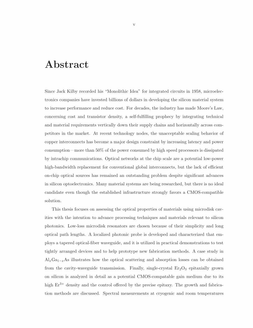
Abstract
Since Jack Kilby recorded his “Monolithic Idea” for integrated circuits in 1958, microelec-
tronics companies have invested billions of dollars in developing the silicon material system
to increase performance and reduce cost. For decades, the industry has made Moore’s Law,
concerning cost and transistor density, a self-fulfilling prophecy by integrating technical
and material requirements vertically down their supply chains and horizontally across com-
petitors in the market. At recent technology nodes, the unacceptable scaling behavior of
copper interconnects has become a major design constraint by increasing latency and power
consumption—more than 50% of the power consumed by high speed processors is dissipated
by intrachip communications. Optical networks at the chip scale are a potential low-power
high-bandwidth replacement for conventional global interconnects, but the lack of efficient
on-chip optical sources has remained an outstanding problem despite significant advances
in silicon optoelectronics. Many material systems are being researched, but there is no ideal
candidate even though the established infrastructure strongly favors a CMOS-compatible
solution.
This thesis focuses on assessing the optical properties of materials using microdisk cav-
ities with the intention to advance processing techniques and materials relevant to silicon
photonics. Low-loss microdisk resonators are chosen because of their simplicity and long
optical path lengths. A localized photonic probe is developed and characterized that em-
ploys a tapered optical-fiber waveguide, and it is utilized in practical demonstrations to test
tightly arranged devices and to help prototype new fabrication methods. A case study in
AlxGa1−xAs illustrates how the optical scattering and absorption losses can be obtained
from the cavity-waveguide transmission. Finally, single-crystal Er2O3 epitaxially grown
on silicon is analyzed in detail as a potential CMOS-compatable gain medium due to its
high Er3+ density and the control offered by the precise epitaxy. The growth and fabrica-
tion methods are discussed. Spectral measurements at cryogenic and room temperatures
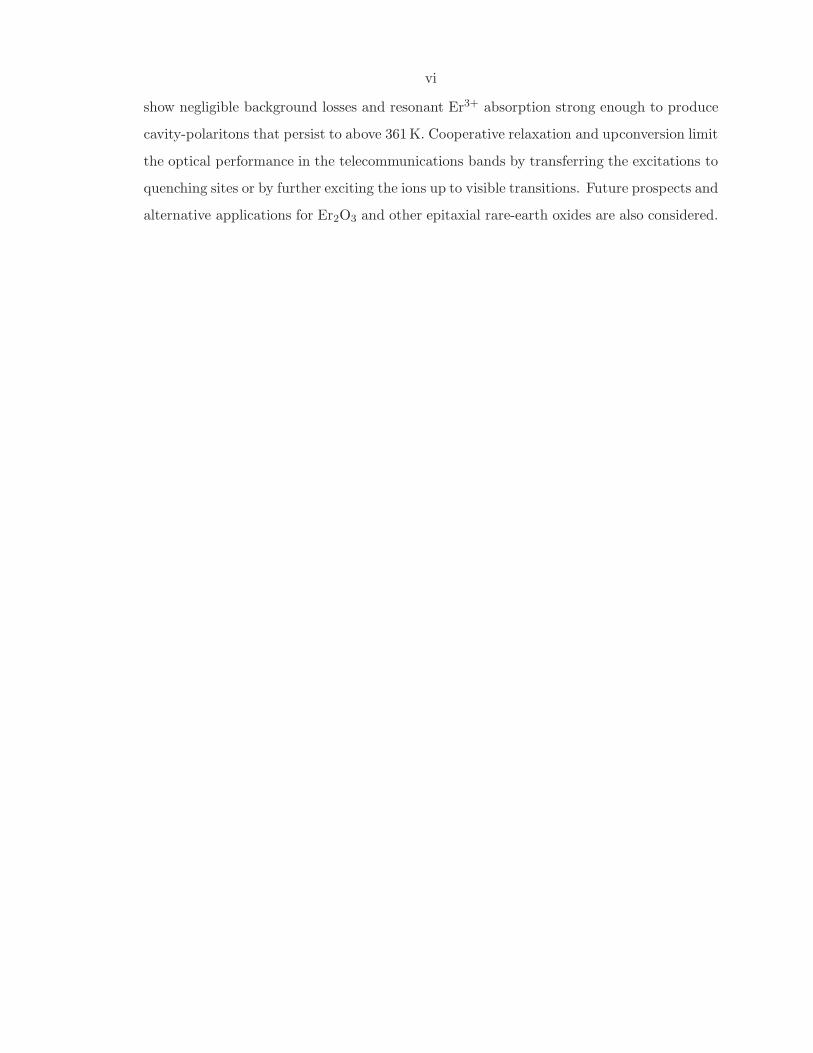
vi
show negligible background losses and resonant Er3+ absorption strong enough to produce
cavity-polaritons that persist to above 361 K. Cooperative relaxation and upconversion limit
the optical performance in the telecommunications bands by transferring the excitations to
quenching sites or by further exciting the ions up to visible transitions. Future prospects and
alternative applications for Er2O3 and other epitaxial rare-earth oxides are also considered.
vii
Contents
Acknowledgments iv
Abstract v
Glossary of Acronyms xii
Preface xiv
1 Microdisk Optical Cavities 1
1.1 Quasi-normal Modes . . . . . . . . . . . . . . . . . . . . . . . . . . . . . . . 3
1.2 Coupled-Mode Theory . . . . . . . . . . . . . . . . . . . . . . . . . . . . . . 8
1.2.1 Coherent Backscattering . . . . . . . . . . . . . . . . . . . . . . . . . 10
1.2.2 Microdisk-Waveguide Coupling . . . . . . . . . . . . . . . . . . . . . 12
1.3 Cavity Parameters . . . . . . . . . . . . . . . . . . . . . . . . . . . . . . . . 17
2 “Dimpled” Fiber-Taper Probe 21
2.1 Taper Pulling and Molding . . . . . . . . . . . . . . . . . . . . . . . . . . . 22
2.2 Microphotonic Testing with a Dimple-Taper Waveguide . . . . . . . . . . . 25
2.2.1 Noise Measurements . . . . . . . . . . . . . . . . . . . . . . . . . . . 27
2.2.2 Dense Si Microdisk Array . . . . . . . . . . . . . . . . . . . . . . . . 29
2.2.3 Planar Si-SiO2 Microring via RIE Processing . . . . . . . . . . . . . 31
2.2.4 Planar Si-SiO2 Microring via LOCOS Processing . . . . . . . . . . . 32
2.3 Conclusions . . . . . . . . . . . . . . . . . . . . . . . . . . . . . . . . . . . . 35
3 Linear Absorption in AlGaAs and GaAs Microcavities 36
3.1 AlxGa1−xAs Samples and Processing . . . . . . . . . . . . . . . . . . . . . . 37
3.2 Estimation of Scattering and Absorption Rates . . . . . . . . . . . . . . . . 39
viii
4 Optical Processes in Epitaxial c-Er2O3 on Silicon 43
4.1 Rare-Earth Ions in the R2O3 Bixbyite Lattice . . . . . . . . . . . . . . . . . 44
4.1.1 Growth . . . . . . . . . . . . . . . . . . . . . . . . . . . . . . . . . . 47
4.1.2 Processing . . . . . . . . . . . . . . . . . . . . . . . . . . . . . . . . . 50
4.2 Optical Properties . . . . . . . . . . . . . . . . . . . . . . . . . . . . . . . . 52
4.2.1 Absorption and Emission Spectra for the 4I13/2→4I15/2 Transition . 53
4.2.2 Upconversion . . . . . . . . . . . . . . . . . . . . . . . . . . . . . . . 57
4.2.3 Effective 4I13/2 Lifetime . . . . . . . . . . . . . . . . . . . . . . . . . 60
4.2.4 Power-Dependent Radiative Efficiency . . . . . . . . . . . . . . . . . 63
4.2.5 Cavity Polaritons . . . . . . . . . . . . . . . . . . . . . . . . . . . . . 67
4.2.5.1 Low-Temperature Polaritons . . . . . . . . . . . . . . . . . 69
4.2.5.2 High-Temperature Polaritons . . . . . . . . . . . . . . . . . 76
4.2.6 Rate Equation Estimates . . . . . . . . . . . . . . . . . . . . . . . . 82
4.3 Conclusions . . . . . . . . . . . . . . . . . . . . . . . . . . . . . . . . . . . . 84
A Experimental Supplement 86
A.1 Mach-Zehnder Interferometer . . . . . . . . . . . . . . . . . . . . . . . . . . 86
A.2 Pulse Optimization for EOSPACE Modulators . . . . . . . . . . . . . . . . 90
A.3 Effective Index for the HE11 Mode . . . . . . . . . . . . . . . . . . . . . . . 92
A.4 Coherent Coupling to a Uniform Density of Dipoles . . . . . . . . . . . . . . 92
B Calculation of the β-Factor for Er2O3 Microdisks 95
Bibliography 98
ix
List of Figures
1.1 Microdisk geometry . . . . . . . . . . . . . . . . . . . . . . . . . . . . . . . . 4
1.2 FEM simulation of field components for TE and TM microdisk modes . . . . 7
1.3 Comparison of effective-index and FEM models for microdisk QNMs . . . . . 9
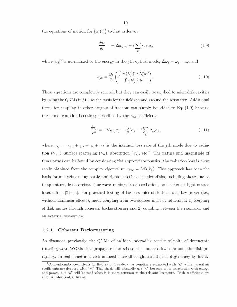
1.4 Illustration of microdisk-waveguide coupling . . . . . . . . . . . . . . . . . . . 13
1.5 Power conservation and phase for coupling to a doublet resonance . . . . . . 14
1.6 Comparison of cavity loading for singlet and doublet modes . . . . . . . . . . 17
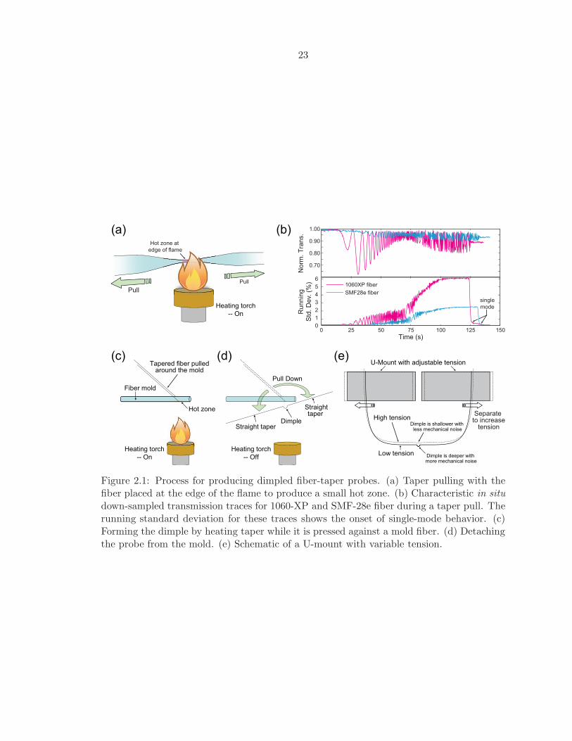
2.1 Process for producing dimpled fiber-taper couplers . . . . . . . . . . . . . . . 23
2.2 The “dimpled” fiber-taper waveguide probe . . . . . . . . . . . . . . . . . . . 25
2.3 Dimple taper profile as a function of fiber tension . . . . . . . . . . . . . . . 26
2.4 Basic arrangement for microcavity transmission measurements . . . . . . . . 26
2.5 Reducing mechanical noise through higher taper tension. . . . . . . . . . . . 28
2.6 Testing demonstration: dense microdisk array . . . . . . . . . . . . . . . . . . 30
2.7 Testing demonstration: planar microring . . . . . . . . . . . . . . . . . . . . 31
2.8 Testing demonstration: LOCOS process development . . . . . . . . . . . . . 33
3.1 AlxGa1−xAs microdisk resonators . . . . . . . . . . . . . . . . . . . . . . . . 38
3.2 Summary of measured resonance parameters for AlxGa1−xAs microdisks . . . 38
3.3 Sample surface roughness measurement on a AlGaAs microdisk . . . . . . . . 40
4.1 Rare-earth ions in the R2O3 lattice . . . . . . . . . . . . . . . . . . . . . . . . 45
4.2 Er2O3 grown via ALE on Si(111) . . . . . . . . . . . . . . . . . . . . . . . . . 48
4.3 Processing Er2O3 microdisk cavities . . . . . . . . . . . . . . . . . . . . . . . 51
4.4 Er2O3 microdisk transmission spectrum (R ≈ 20µm) . . . . . . . . . . . . . 53
4.5 Emission and absorption spectra for the 4I13/2→4I15/2 transition . . . . . . . 54
4.6 Sample fits to cavity transmission resonances . . . . . . . . . . . . . . . . . . 55
x
4.7 Upconversion behavior . . . . . . . . . . . . . . . . . . . . . . . . . . . . . . . 59
4.8 Measurement of the 4I13/2 lifetime. . . . . . . . . . . . . . . . . . . . . . . . . 61
4.9 Power-dependent radiative efficiency of the 4I13/2→4I15/2 transition . . . . . 65
4.10 Cavity-polariton spectra at T = 8.6 K . . . . . . . . . . . . . . . . . . . . . . 70
4.11 Dispersion and absorption for Z1→Yx transitions at T = 8.6 K . . . . . . . . 75
4.12 Spoked microdisks used for high-temperature polariton measurements . . . . 77
4.13 Schematic layout for polariton pump-probe measurements. . . . . . . . . . . 78
4.14 Observation of Rabi splitting at high temperature . . . . . . . . . . . . . . . 80
A.1 Calibration of wide spectra using a fiber-based Mach-Zehnder interferometer 89
A.2 Comparison of neff values for the HE11 mode . . . . . . . . . . . . . . . . . . 93
B.1 Comparison of calculated and measured emission into Er2O3 WGMs . . . . . 97
xi
List of Tables
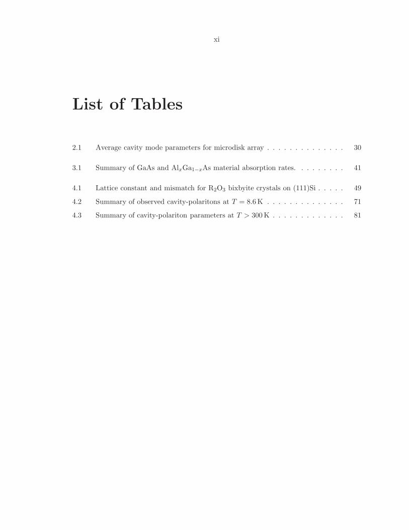
2.1 Average cavity mode parameters for microdisk array . . . . . . . . . . . . . . 30
3.1 Summary of GaAs and AlxGa1−xAs material absorption rates. . . . . . . . . 41
4.1 Lattice constant and mismatch for R2O3 bixbyite crystals on (111)Si . . . . . 49
4.2 Summary of observed cavity-polaritons at T = 8.6 K . . . . . . . . . . . . . . 71
4.3 Summary of cavity-polariton parameters at T > 300 K . . . . . . . . . . . . . 81
xii
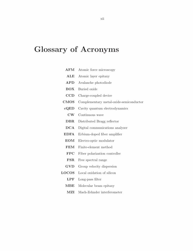
Glossary of Acronyms
AFM Atomic force microscopy
ALE Atomic layer epitaxy
APD Avalanche photodiode
BOX Buried oxide
CCD Charge-coupled device
CMOS Complementary metal-oxide-semiconductor
cQED Cavity quantum electrodynamics
CW Continuous wave
DBR Distributed Bragg reflector
DCA Digital communications analyzer
EDFA Erbium-doped fiber amplifier
EOM Electro-optic modulator
FEM Finite-element method
FPC Fiber polarization controller
FSR Free spectral range
GVD Group velocity dispersion
LOCOS Local oxidation of silicon
LPF Long-pass filter
MBE Molecular beam epitaxy
MZI Mach-Zehnder interferometer
xiii
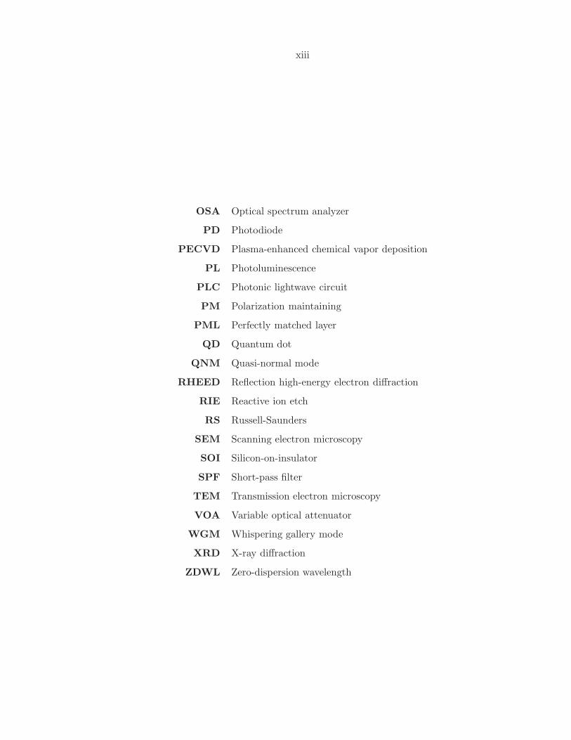
OSA Optical spectrum analyzer
PD Photodiode
PECVD Plasma-enhanced chemical vapor deposition
PL Photoluminescence
PLC Photonic lightwave circuit
PM Polarization maintaining
PML Perfectly matched layer
QD Quantum dot
QNM Quasi-normal mode
RHEED Reflection high-energy electron diffraction
RIE Reactive ion etch
RS Russell-Saunders
SEM Scanning electron microscopy
SOI Silicon-on-insulator
SPF Short-pass filter
TEM Transmission electron microscopy
VOA Variable optical attenuator
WGM Whispering gallery mode
XRD X-ray diffraction
ZDWL Zero-dispersion wavelength
xiv
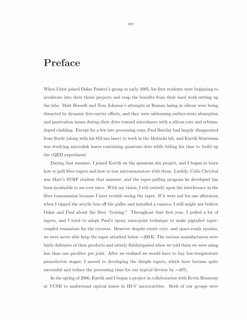
Preface
When I first joined Oskar Painter’s group in early 2005, his first students were beginning to
accelerate into their thesis projects and reap the benefits from their hard work setting up
the labs. Matt Borselli and Tom Johnson’s attempts at Raman lasing in silicon were being
thwarted by dynamic free-carrier effects, and they were addressing surface-state absorption
and passivation issues during their drive toward microlasers with a silicon core and erbium-
doped cladding. Except for a few late processing runs, Paul Barclay had largely disappeared
from Steele (along with his 852-nm laser) to work in the Mabuchi lab, and Kartik Srinivasan
was studying microdisk lasers containing quantum dots while biding his time to build up
the cQED experiment.
During that summer, I joined Kartik on the quantum dot project, and I began to learn
how to pull fiber-tapers and how to test microresonators with them. Luckily, Colin Chrystal
was Matt’s SURF student that summer, and the taper-pulling program he developed has
been invaluable to me ever since. With my vision, I rely entirely upon the interference in the
fiber transmission because I have trouble seeing the taper. If it were not for one afternoon
when I ripped the acrylic box off the puller and installed a camera, I still might not believe
Oskar and Paul about the fiber “bowing.” Throughout that first year, I pulled a lot of
tapers, and I tried to adapt Paul’s epoxy microjoint technique to make pigtailed taper-
coupled resonators for the cryostat. However despite exotic cryo- and space-ready epoxies,
we were never able keep the taper attached below ∼200 K. The various manufacturers were
fairly defensive of their products and utterly flabbergasted when we told them we were using
less than one picoliter per joint. After we realized we would have to buy low-temperature
piezoelectric stages, I moved to developing the dimple tapers, which have become quite
successful and reduce the processing time for our typical devices by ∼40%.
In the spring of 2006, Kartik and I began a project in collaboration with Kevin Hennessy
at UCSB to understand optical losses in III-V microcavities. Both of our groups were
xv
working towards the strong coupling regime in cQED using quantum dots. The original
objective was to compare Kartik’s RIE (Ar:Cl2) with Kevin’s wet chemical etches (HBr)
of AlxGa1−xAs and to understand why both methods seemed to underperform at shorter
wavelengths. Unfortunately, the only method to assess the procedures (and not just lone
exceptional devices) was to study many modes on many resonators at many wavelengths and
identify statistical trends in the resulting heap of data. Since Kartik and Oskar were pretty
sure this was a material issue, we reduced the scope to study only the HBr process (Kevin
also gained a processing assistant so he would not actually have to make these devices).
I got a lot of practice taper testing and quickly learned about microdisks, especially once
we realized the edge roughness was different on our two material samples. Through the
early summer, I worked to pile up data between classes and being hammered by the APh 24
lab, located in the lifeless cave that would shortly become the Kavli Nanoscience Institute.
During that time I also decided to switch off the quantum dot project. Kartik was running
past microlasers and master equations while I was still dealing with resonator coupling
and holography labs. Ironically, Matt was simultaneously developing some more advanced
single-shot techniques to separate scattering and absorption that would have saved me a
lot of time and effort—I found out about these while reading his thesis a few months after
I had finished taking my data.
So I packed my bags and landed in silicon photonics. After doing some basic silicon
testing for the dimple paper, our intention was that I would continue work with the Er3+-
doped silica from InPlane Photonics that Matt had left after his graduation. However,
that fall we were presented with the opportunity to switch our DARPA program to work
with Translucent in developing Er2O3. Oskar and I made the switch realizing the big-
risk/big-reward potential. At the very least, it would temporarily free me from low-loss
surface-senstive processing and give us exclusive access to new material (unlike the crowded
field of erbium-doped glasses). I had already broken my rule #1 for choosing thesis topics
(no cryogenics) so breaking rule #2 (no exotic materials) did not seem that bad—especially
since the growers (Vijit Sabnis and Homan Yuen) were ready and willing to ship me more
material than I could ever deal with. I am still waiting to break rule #3 (no ultrahigh
vacuum) and give MBE a shot.
In retrospect, we should have given more credence to some of our initial minor concerns,
but we jumped in. Tom gave me a great head start on the processing by throwing the Er2O3
xvi
films at a battery of chemicals, of which most did nothing. I proceeded optimistically as
Homan and Vijit addressed material problems at about the same pace I was figuring out
the processing and testing aspects. The first disks I made with H2SO4 produced weak, but
measurable, PL and exhibited the transmission features that would later be identified as
cavity-polaritons at room temperature. By March of 2007, we were beginning to become
concerned with the upconversion and our inability to see any absorption saturation. In
June, I figured out the Ar+ milling, made a bunch of samples, and then did not go back
into the clean room for over a year (except to train people and pester Raviv Perahia). Once
free from the clean room, I began gaining dominion over equipment in the test lab, which
has provided me far too much contact with the New Focus laser repair department.
That fall, after a year on the project, we were beginning to get frustrated, but I keep
myself busy with absorption spectra, radiative efficiency, upconversion, and polaritons at
high and low temperatures. Vijit and Homan had moved on to work on starting a new
company, but Translucent was bringing on new people. At this point, I also began some
adventures into cQED by helping Kartik with some of his quantum dot measurement and
testing my own disks in the cryostat. I worked throughout 2008 investigating the lifetime
and polariton behaviors. Some of the data could have been obtained more quickly with
unprocessed films and free-space optics. However, my unorthodox measurements fit within
our microcavity infrastructure, and we were always optimistic that we would uncover some
physics that would allow us to quickly proceed. Although with the rare-earth studies from
the 1970s and a few rate equation parameters in hand, a coherent picture was emerging
that Er2O3 is not a suitable laser material, and the weak coherent coupling to each ion
made the ubiquitous Rabi splitting depressingly classical. I began a few last-ditch efforts to
achieve lasing that pushed our equipment to the limits and the material beyond its damage
threshold because we had invested a lot of time and energy. A Λ-system laser between
carefully chosen Stark levels at 8 K is a viable option, but the benefits probably do not
outweigh the effort. I decided to leave many questions unanswered concerning upconversion
lasing at green wavelengths in the current material after burning standing-wave gratings into
three disks and outright vaporizing a fourth. There is a subtle lesson here about knowing
when to terminate an experiment.
While Er2O3 did not live up to its promise, these rare-earth oxide films still have consid-
erable potential especially for controlling the emission spectrum and converting absorbed
xvii
photons to other wavelengths using Y2O3 or Gd2O3 alloys. I was exposed to a wide range of
photonics and atomic physics trawling for immediate applications and results to utilize the
current material, which really is an initial step in a much more ambitious material science
and engineering program. Even though much of this thesis is focused on absorption rather
than emission, I take solace in the difficult road to Maiman’s first ruby laser and that a com-
mercially acceptable solution still does not exist to generate gain for optical interconnects
on CMOS microelectronics.
After presenting the formalism for coupling to WGM cavities used throughout these
measurements, this thesis is divided according to material systems. Silicon microresonators
are presented in chapter 2 with details of the dimpled taper probes, which initially saw
their greatest use in prototyping Si devices and fabrication methods. A sample analysis of
loss in AlxGa1−x is presented in chapter 3, and chapter 4 concentrates on Er2O3. Ancillary
experimental and theoretical details are reserved for the appendices.
C. P. Michael
Pasadena, CA
May 2009
1
Chapter 1
Microdisk Optical Cavities
The resonant circulation of electromagnetic waves enables a variety of macroscopic systems
from lasers to interferometric gravitational wave detectors, but recent pressure from the
telecommunications and microelectronics industries, along with more fundamental research
programs, has driven the development of wavelength-scale optical cavities, waveguides, and
other components. Microphotonic cavities can be designed to give a large electric field
strength per photon, a sparse spectrum of optical modes, and great sensitivity to the struc-
ture’s surfaces [1, 2]. By combining these attributes with a high circulating intensity (i.e.,
low field decay rate for the optical mode), microcavity physics is central to many sub-
jects including low-threshold and “thresholdless” lasers [3], control of spontaneous emission
through the Purcell Effect [4,5], nonperturbative light-matter interactions [2,6], low-power
nonlinear optics [7, 8], chemical and biological “lab-on-a-chip” devices [9], and cavity op-
tomechanics [10].
Several microresonator geometries exist beyond the canonical Fabry-Perot cavity that
can be optimized for different applications. Planar cavities with distributed Bragg reflectors
(DBRs) require little etching and are commonly used with epitaxially grown material, as in
exciton-polariton measurements with III-V and II-VI quantum wells [11,12]. Similar studies
with organic emitters, such as cyanine dyes in a J-aggregate structure [13], are possible by
spin coating the organic material onto a wafer with a single DBR and then depositing a
metal film to form the top mirror. Vertically etching a planar cavity to form a micropillar
offers greater lateral mode confinement and more directional coupling through the top
mirror into a single output mode, which has been used to efficiently collect single photon
pulses [14]. Photonic crystals [15,16] utilize Bragg reflection in multiple dimensions to open
electromagnetic band gaps and to achieve a high electric field strength (per photon) [17]
2
without a dielectric discontinuity at the center of the cavity [18], and whispering-gallery
microresonators (e.g., spheres [19], disks [20], and toroids [21]) provide a rich spectrum of
modes with low intrinsic loss.
While significant work is focused on cavity design, material properties are of equal
concern in many applications. These properties include both bulk quantities (absorption
coefficient, radiative and nonradiative relaxation rates, etc.) and surface quantities (absorp-
tion by surface states, surface recombination velocity, etc.). Microcavities are a convenient
tool for assessing material quality because they offer a long effective interaction length and
measurable losses associated with input/output coupling. Device attributes associated with
material processing (surface roughness, passivation layers, etc.) can also be investigated once
bulk effects are adequately understood.
To maximize their utility for material studies, microcavities should be trivial to design
with low intrinsic loss, easy to fabricate in a variety of materials, and straightforward
to identify fabricated imperfections without optical measurements. Compared to other
geometries, microdisk resonators offer an attractive combination of simplicity and material
flexibility. Disks with diameters (thicknesses) ≫λo/nd (>λo/2nd) support a large number
of modes with very low radiation loss and require only a single material layer,1 where λo is
the free-space wavelength and nd is the refractive index of the disk material. The quality of
the fabrication process for these devices can be easily evaluated by the surface roughness,
unlike photonic crystals that require fault-tolerant designs [22] or precise simulation of the
as-fabricated structures [23]. Microdisks are also robust against subtle leaky geometric
variations as in micropillars [24, 25] and microrings [26].2 Microspheres and toroids offer
many of the same advantages along with the lowest optical loss for any microcavity structure,
which makes these devices extremely sensitive to refractive index changes in their modes’
evanescent tail [28–30], but the glass reflow procedure limits their material range to doped
silica (e.g., through sol-gel deposition [31, 32] or ion implantation [33, 34]) or postreflow
surface coatings [35, 36]. While replica molding techniques extend the toroid’s versatility
to cured polymers [37], processing methods for crystalline toroids (e.g., silicon [38]) are not
as mature as for microdisks. In this chapter, the quasi-normal whispering gallery modes
1Excluding a sacrificial substrate that must be undercut to form the disk’s pedestal.2The whispering gallery modes of a microdisk with low refractive index can couple to modes with the
same momentum in a high-index pedestal, which then radiate down into the substrate. However, this losschannel can be easily ameliorated by further undercutting as in Ref. [27].
3
(WGMs) of a microdisk resonator are discussed, and the coupled-mode theory and cavity
parameters used throughout this work are presented.
1.1 Quasi-normal Modes
The normal modes of a system are solutions to the appropriate time-independent wave
equation with the condition that the wave amplitude vanishes at the system boundary
(either at infinity or the boundary of a more suitable domain), as for the optical field
in an ideal Fabry-Perot cavity or the elastic vibrations of a perfectly isolated rigid body.
Under this constraint, the field magnitude is conserved, and the eigenvalues are real. The
quasi-normal modes (QNM) of an open system are solutions to the same wave equation
with an outgoing traveling-wave boundary condition that causes the field to decay [39].
In this classical analysis, the nature of the coupling to the bath of radiation modes is
concealed unlike the quantum treatment of dissipation where the bath’s degrees of freedom
are included and later removed using specific assumptions [40].
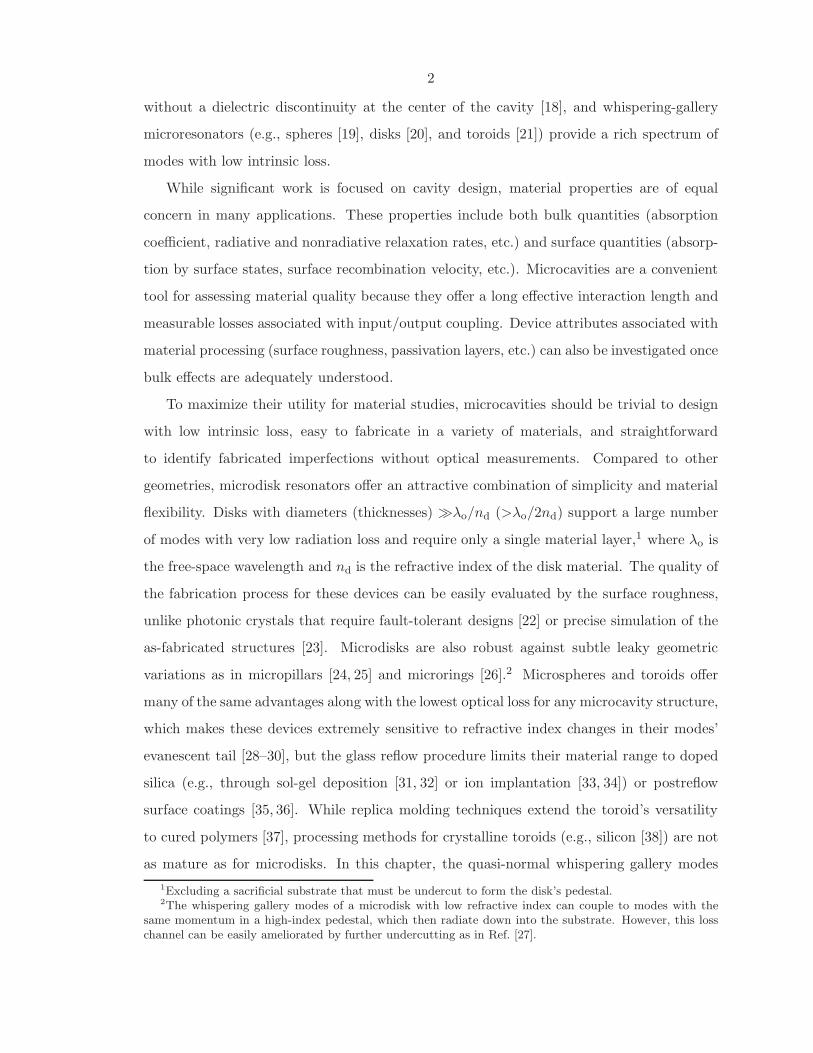
The microdisk structure consists of a planar slab with radius R and height h as in
Fig. 1.1(a)—we assume the pedestal and substrate are undercut far enough to have little
overlap with the cavity field. While analytic solutions for this geometry do not exist, the
cavity modes can be found with reasonable accuracy using a 2D effective-index model.
In Refs. [41, 42], the QNMs are further simplified by using exponential decay to describe
fields outside the cavity. These real normal-mode eigenvalues do not describe radiation
loss, but this analysis can be extended to include radiating fields and complex eigenvalues.3
Further insight into the modes’ behavior can also be gained from a conformal coordinate
transformation and the WKB approximation [44, 45], but semianalytic solutions without
this transform have been most useful for quickly evaluating dispersion characteristics and
providing accurate starting values for targeted numerical eigenvalue solvers.
Starting with the electromagnetic wave equation for a linear piecewise-homogeneous
medium in the absence of free charges and currents,
∇2 ~F − n2(~r)
c2∂2 ~F
∂t2= 0, (1.1)
where ~F ∈ ~E, ~H, the standard linear constitutive relations are ~D = ǫ(~r) ~E and ~B =
3This QNM analysis was explored prior to its publication by Heebner et al. [43].
4
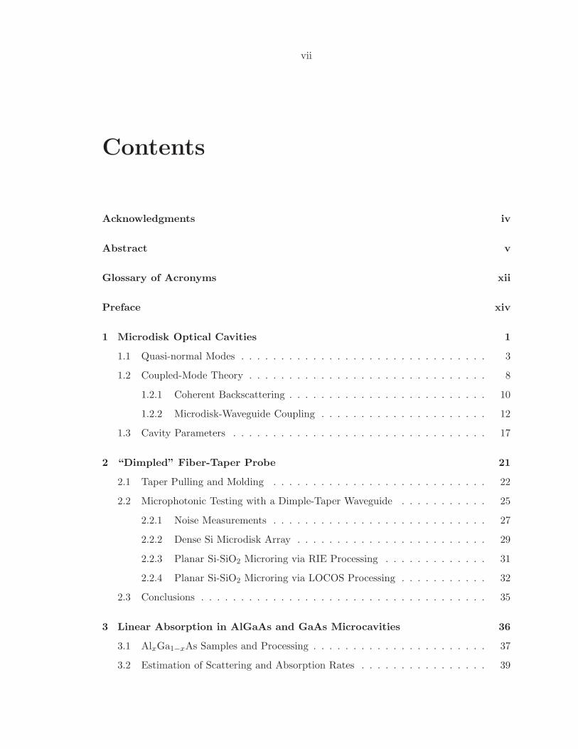
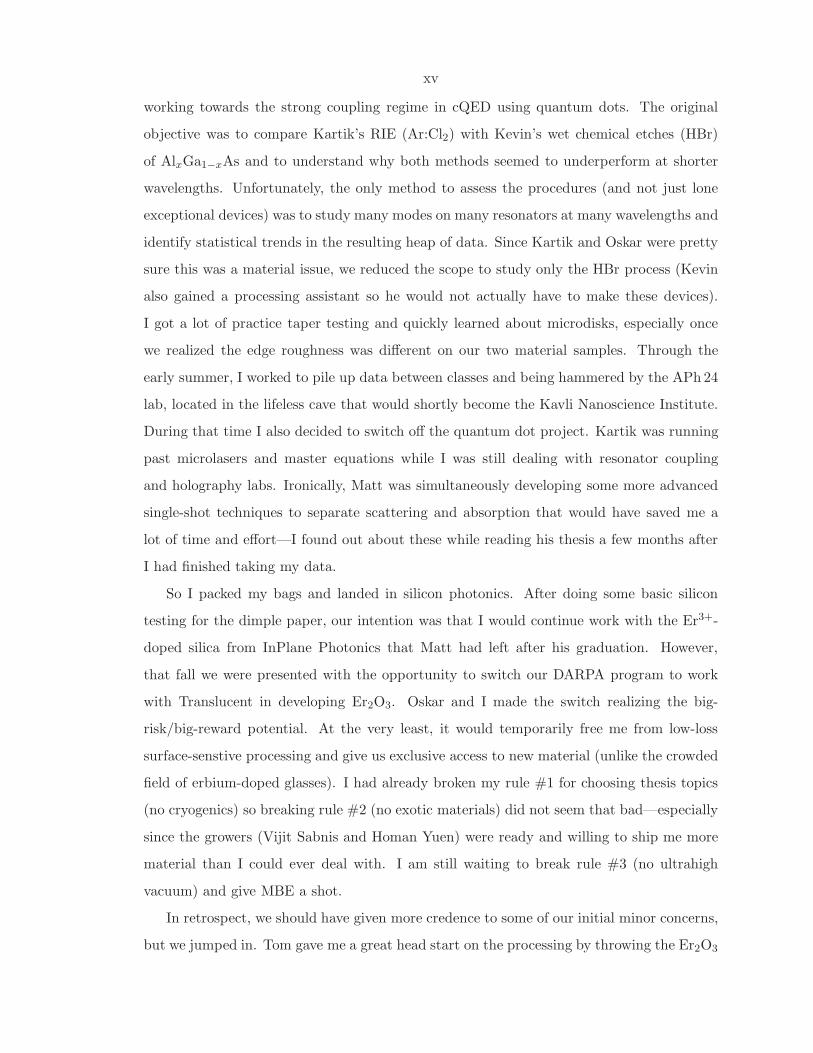
2 µm
(b)(a)
r
z
φ
R
h
Figure 1.1: (a) Perspective sketch of a microdisk and the e±imϕ field dependence for asecond-order mode (m = 35, p = 2). (b) SEM image of a microdisk array fabricated fromsilicon-on-insulator (SOI)—i.e., Si disks with SiOx pedestals on a Si substrate.
µ(~r) ~H ≈ µo~H, c = 1/
√ǫoµo is the speed of light in vacuum, and n(~r) =
√
ǫ(~r)/ǫo is the
refractive index. By considering only oscillatory solutions ~F (~r, t) = ~F (~r)e−iωt, the time-
independent wave equation in cylindrical coordinates becomes
(
∂2
∂r2+
1
r
∂
∂r+
1
r2∂2
∂ϕ2+
∂2
∂z2+ k2
on2(~r)
)
~F (~r) = 0, (1.2)
where physical fields are given by ℜ(~F ), and ko = ω/c is the desired eigenvalue representing
the mode’s wavevector in free space. To account for material dispersion, n(ω) is calculated
by fitting the Sellmeier formula to published data for Si and SiOx [46] and by using a
simplified interband-transition model for AlxGa1−xAs [47]. Since data is unavailable, we
model Er2O3 as nondispersive (n = 2.0); Sellmeier coefficients are available for Y2O3 but
would not account for the optical transitions in the Er3+ ions [48].
The high refractive index contrast along z for thin microdisks restricts the out-of-plane
momentum for WGMs and allows the system to be simplified using a self-consistent effective-
index model. This method also builds an intuitive picture of WGM behavior based on how
the mode’s total momentum is roughly partitioned along r, ϕ, and z. By assuming the
mode’s momentum along z is the same as in the analogous slab waveguide, the 3D disk with
refractive index nd (cladding index no) can be treated as a 2D circle with a refractive index
neff , where neff is the effective index for the fundamental mode of a symmetric slab waveguide
with the same h and nd following the calculation in Ref. [49]. Under this assumption
which is usually valid except for h ≫ λo/2nd, the Maxwell’s Equations relating the field
components partially decouple giving two orthogonally polarized cavity modes. The TE
5
modes have non-zero Er, Eϕ,Hz fields, and the TM modes consist of Hr,Hϕ, Ez, where
the r-component identifies the TE-TM character similar to slab waveguides. These QNMs
can be obtained by solving Eq. (1.2) for Fz, where Fz = Hz and Ez for the TE and TM
modes, respectively. Using separation of variables, Eq. (1.2) can be rewritten for solutions
of the form Fz = R(r)A(ϕ)Z(z):
∂2Z
∂z2+ k2
o [n2(z) − n2
eff ]Z = 0, (1.3a)
∂2A
∂ϕ2+m2
A = 0, (1.3b)
(
r2∂2
∂r2+ r
∂
∂r+ r2k2
on2eff(r) −m2
)
R = 0, (1.3c)
where neff(r) = neff at r < R and neff(r) = no at r > R. Equation 1.3a effectively accounts
for the out-of-plane propagation (Z ≈ e±iβ⊥z) with
β2⊥ + k2
on2eff = k2
on2(z), (1.4)
where β⊥ is the propagation constant normal to the disk plane and koneff is proportional
to the in-plane momentum. The solutions A = e±imϕ to Eq. (1.3b) describe clockwise and
counterclockwise traveling waves [Fig. 1.1(a)] with angular momentum proportional to the
mode index m, which is an integer since the field must be single valued for ∆ϕ = 2π. These
traveling-wave modes are degenerate due to rotational symmetry [ϕ → −ϕ in Eq. (1.2)].
The radial solution to Eq. (1.3c) is
R =
Jm(koneffr) for r ≤ R,
H(1)m (konor) for r ≥ R,
(1.5)
where Jm(x) and H(1)m (x) are the Bessel and Hankel functions of the first kind.4 Matching
the fields tangential to the disk boundary at r = R gives a transcendental equation for the
complex QNM eigenvalues (ko)
m
koneffR
(
1 − ξno
neff
)
=Jm+1(koneffR)
Jm(koneffR)− ξ
(
no
neff
)
H(1)m+1(konoR)
H(1)m (konoR)
, (1.6)
4Bessel and Hankel functions of the second kind [Ym(x) and H(2)m (x)] are divergent as x → 0 and x → ∞,
respectively.
6
where ξ = n2eff/n
2o for TE modes and ξ = 1 for TM modes.
Equation 1.6 can be solved numerically in the complex plane using a 2D minimization
routine starting near the real axis [ℜ(ko) ≫ ℑ(ko)]. There will be multiple solutions to
Eq. (1.6) for a given angular momentum (m) corresponding to modes of different radial
order p [number of antinodes for Hz or Ez along r as in Fig. 1.1(a)]. The index p also
qualitatively describes the momentum along the radial direction. Hence, the fundamental
(p = 1) radial mode for a given m will have the lowest |ko| because higher p modes will have
a larger total momentum if the angular component is fixed. In general for two modes with
the same |ko| if p1 < p2, then m1 > m2. Microdisks also support modes with higher vertical
order (more than one Fz antinode along z) which can be found with Eq. (1.6) by using neff
for the appropriate order slab mode; however, the devices in this work only support the
fundamental slab modes. For completeness, the condition to cut off the second-order mode
is2h
λo
√
n2d − n2
o < 1, (1.7)
which corresponds to h = 233 nm in Si (nd = 3.476) at λo = 1550 nm; the fundamental TE
and TM modes are never cut off in a symmetric slab waveguide. Throughout this thesis,
microdisk modes are commonly organized in families according to polarization and radial
order (e.g., TEp=2); within these families, consecutive modes (∆m = ±1) have a relatively
small free spectral range, comparable radiation loss, and similar phase velocity at the disk
edge—which is pertinent to WGM-waveguide coupling.
While the effective-index solution provides an efficient method for finding the QNM
eigenvalues with modest computational resources, numerical models using the finite ele-
ment method (FEM) are more flexible for variable structures and calculations involving
the full 3D geometry. Finite-element simulation of axially symmetric resonators can be
accomplished using Comsol’s Multiphysics/Femlab platform by incorporating the eimϕ de-
pendence into a fully vectorial Cartesian waveguide solver.5 In these models, the 3D cavity
and cladding are represented by a cross section in the r-z plane, and a targeted eigenvalue
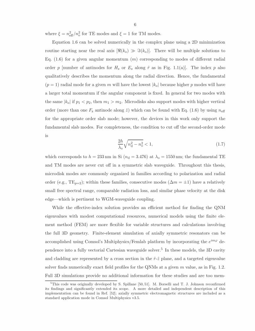
solver finds numerically exact field profiles for the QNMs at a given m value, as in Fig. 1.2.
Full 3D simulations provide no additional information for these studies and are too mem-
5This code was originally developed by S. Spillane [50, 51]. M. Borselli and T. J. Johnson reconfirmedits findings and significantly extended its scope. A more detailed and independent description of thisimplementation can be found in Ref. [52]; axially symmetric electromagnetic structures are included as astandard application mode in Comsol Multiphysics v3.5.
7
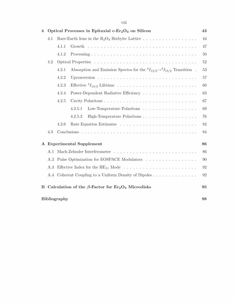
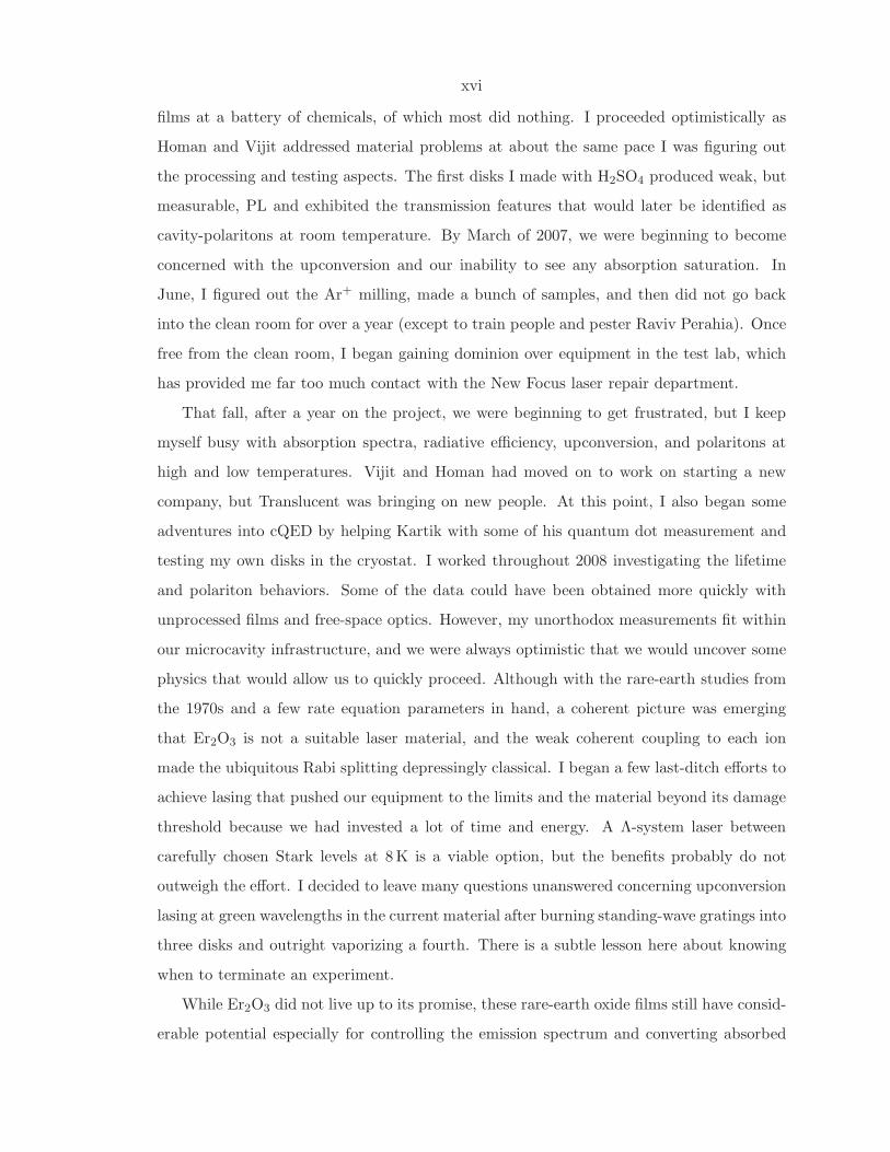
E fi
eld
H fi
eld
→→
r z i(φ) Norm
E fi
eld
H fi
eld
→→
ˆ ˆ ˆHz viewed along z
(a) TE mode: p = 3, m = 65, λ = 1555.1 nm, Qrad > 1016
(b) TM mode: p = 2, m = 35, λ = 1543.5 nm, Qrad = 6900(–) 0 (+)
r
z
φ
r z i(φ) Normˆ ˆ ˆEz viewed along z
Figure 1.2: Sample FEM simulations of field components for (a) TE and (b) TM modesin a Si microdisk with R = 7.5µm and h = 210 nm showing the region 5 ≤ r ≤ 8µm.Simulations in the r-ϕ plane utilize the same neff approximation as Eq. (1.3a), but they areless accurate than the solutions to the r-z FEM models or Eq. (1.6). The notation “i(ϕ)”indicates the Fϕ components are π/2 out of phase.
ory intensive for typical desktop computers.6 When setting the geometry, the disk and
cladding must be bound by perfectly matched layers (PMLs) that allow energy to escape
the simulated domains in order to properly account for radiation losses [53]. These PMLs
have complex anisotropic permittivity and permeability that quickly attenuate fields along
a single direction without producing spurious reflections. By including PMLs thick enough
to fully absorb the radiated waves, both highly confined and highly lossy modes can be
found with ℑ(ko) varying by more than 1014× as in Fig. 1.2. The quantity ℜ(ko)/2ℑ(ko) is
approximately 2π times the number of optical cycles that occurs while the field decays—this
value is later identified as the radiation limited quality factor Qrad.
These quasi-3D FEM models can be used to address two important aspects of real
6Dual-core 2–3 GHz processor, 64-bit operating system, 4GB RAM.
8
microdisks that are not captured by the effective-index approximation: 1) the disk edge
is not perfectly vertical and 2) surface effects. First, the primary objective during disk
fabrication is minimizing surface roughness to reduce scattering losses, and the optimized
anisotropic etches do not generally produce vertical sidewalls. Slanted edges couple the
TE and TM polarizations by breaking the disk’s vertical symmetry, which can occasionally
produce hybrid modes if a TE and a TM mode are nearly degenerate and have the same m.
The TE/TM labels are no longer rigorously accurate with slanted walls because significant
longitudinal components may exist, but modes are conventionally identified as “TE” if
|Er| > |Ez| at the disk’s midplane. For most general considerations, the bevelled edge only
marginally increases the radiation losses [54, 55]. Second, Fig. 1.2 illustrates TM modes
are significantly more sensitive to the top and bottom surfaces while the TE modes have
greater overlap with the sidewall. This difference has practical consequences that will be
discussed later, such as absorption by surface states [56].
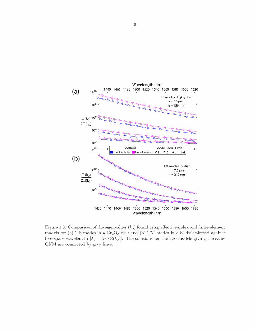
Comparing approximate effective-index solutions with FEM results in Fig. 1.3 for two
disk microdisk devices indicates the effectiveness of Eq. (1.6) to quickly explore wide areas
in parameter space. The approximate solutions take .0.5 s to compute without previous
information about the QNMs. Alternatively, FEM simulations take ∼1–2 min with a rea-
sonable mesh resolution [<0.05λ/n(~r)] and a good initial guess for the desired eigenvalue
(∆λo . 5 nm); however, they can be accelerated (∼10 s) during parametric studies if better
guesses can be supplied (∆λo . 0.2 nm). In Fig. 1.3, the effective-index solutions overesti-
mate λo found using the FEM by 3.6 nm and underestimate ℑ(ko) by 1.9× on average.
1.2 Coupled-Mode Theory
Coupled mode analysis is a general framework to describe the evolution of optical fields due
to perturbations that do not significantly alter the system’s eigenmodes [57]. As is common
in perturbation theories, a total field in a system (driven with a laser at ω = ωℓ) is expanded
as
~E(~r, t) = e−iωℓt∑
j
aj(t) ~Eoj (~r), (1.8)
in terms of slowly varying amplitudes aj(t) and the system’s unperturbed QNM field profiles
~Eoj (~r). For small dielectric perturbations [ǫ(~r) → ǫ(~r) + δǫ(~r)] as treated in Refs. [42, 58],
9
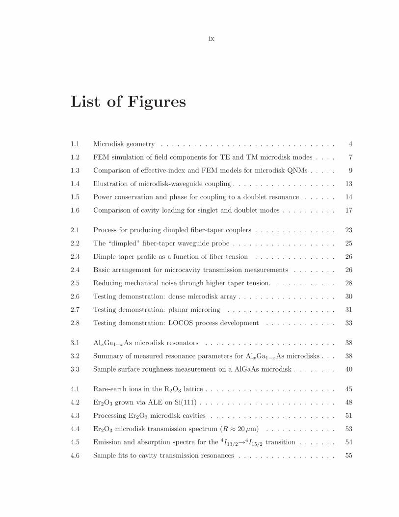
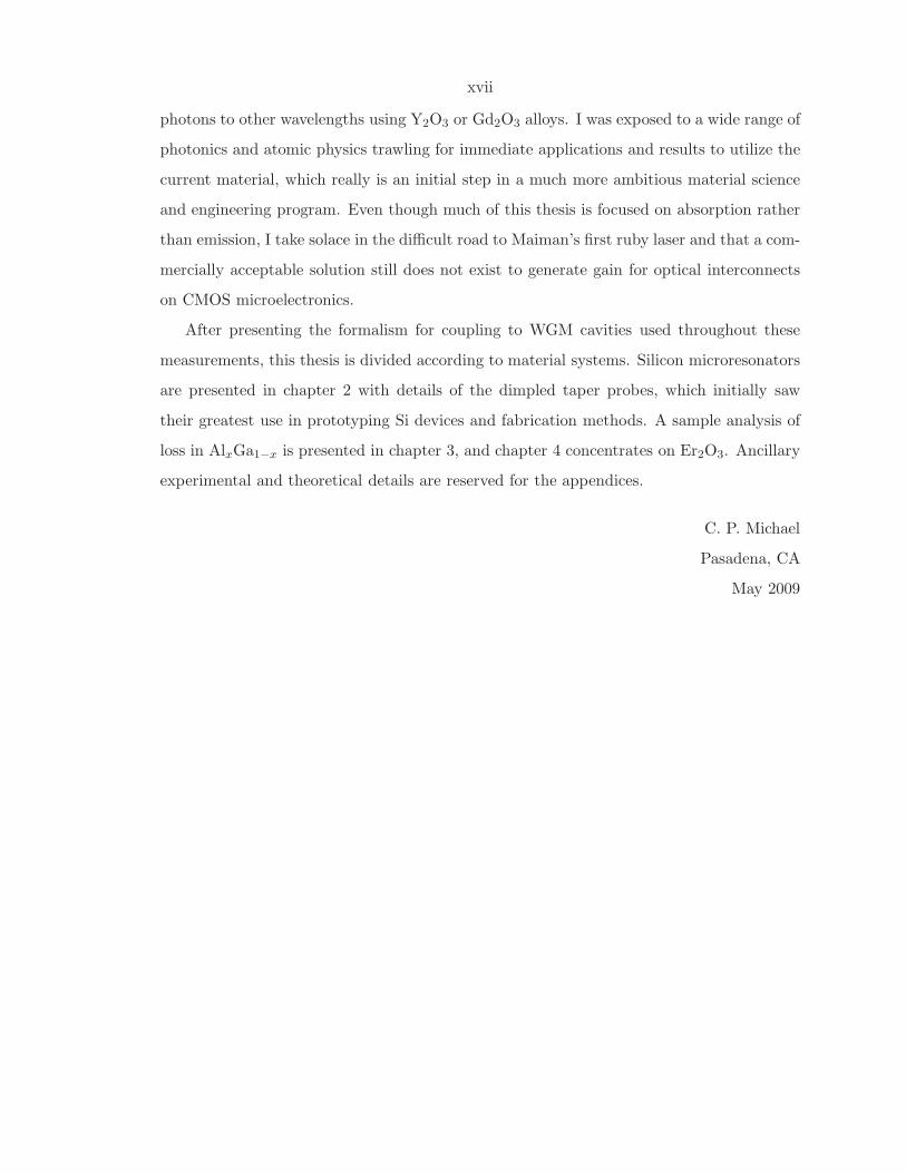
1440 1460 1480 1500 1520 1540 1560 1580 1600 1620
105
Wavelength (nm)1420
1010
1015
102
104
106
108
10101440 1460 1480 1500 1520 1540 1560 1580 1600 1620
Wavelength (nm)
TE modes: Er2O3 disk
r = 20 μm
h = 150 nm
TM modes: Si disk
r = 7.5 μm
h = 210 nm
Method Mode Radial OrderEffective Index Finite Element 1 2 3 4
(a)
(b)
ℜ(k0)
2ℑ(k0)
ℜ(k0)
2ℑ(k0)
Figure 1.3: Comparison of the eigenvalues (ko) found using effective-index and finite-elementmodels for (a) TE modes in a Er2O3 disk and (b) TM modes in a Si disk plotted againstfree-space wavelength [λo = 2π/ℜ(ko)]. The solutions for the two models giving the sameQNM are connected by grey lines.
10
the equations of motion for aj(t) to first order are
daj
dt= −i∆ωjaj + i
∑
k
κjkak, (1.9)
where |aj |2 is normalized to the energy in the jth optical mode, ∆ωj = ωj − ωℓ, and
κjk =ωℓ
2
(∫
δǫ( ~Eoj )∗ · ~Eo
kd~r∫
ǫ| ~Eoj |2d~r
)
. (1.10)
These equations are completely general, but they can easily be applied to microdisk cavities
by using the QNMs in §1.1 as the basis for the fields in and around the resonator. Additional
terms for coupling to other degrees of freedom can simply be added to Eq. (1.9) because
the modal coupling is entirely described by the κjk coefficients:
daj
dt= −i∆ωjaj −
γj,i
2aj + i
∑
k
κjkak, (1.11)
where γj,i = γrad + γss + γa + · · · is the intrinsic loss rate of the jth mode due to radia-
tion (γrad), surface scattering (γss), absorption (γa), etc.7 The nature and magnitude of
these terms can be found by considering the appropriate physics; the radiation loss is most
easily obtained from the complex eigenvalue: γrad = 2cℑ(ko). This approach has been the
basis for analyzing many static and dynamic effects in microdisks, including those due to
temperature, free carriers, four-wave mixing, laser oscillation, and coherent light-matter
interactions [59–63]. For practical testing of low-loss microdisk devices at low power (i.e.,
without nonlinear effects), mode coupling from two sources must be addressed: 1) coupling
of disk modes through coherent backscattering and 2) coupling between the resonator and
an external waveguide.
1.2.1 Coherent Backscattering
As discussed previously, the QNMs of an ideal microdisk consist of pairs of degenerate
traveling-wave WGMs that propagate clockwise and counterclockwise around the disk pe-
riphery. In real structures, etch-induced sidewall roughness lifts this degeneracy by break-
7Conventionally, coefficients for field amplitude decay or coupling are denoted with “κ” while magnitude
coefficients are denoted with “γ.” This thesis will primarily use “γ” because of its association with energyand power, but “κ” will be used when it is more common in the relevant literature. Both coefficients areangular rates (rad/s) like ωj .
11
ing the rotational symmetry and couples the counterpropagating WGMs through coherent
Rayleigh backscattering. Cursory inspection of Eq. (1.10) gives κm,−m = κ∗−m,m ≡ |κcb|eiϕo
because the two modes only differ in their angular dependence (e±imϕ); for convenience the
perturbation δǫ(~r) is real and chosen such that κm,m = 0. In addition, the integral in the
numerator of Eq. (1.10) makes |κcb| proportional to the ±2m spatial Fourier component
of the roughness:∫
δǫ(ϕ)( ~Eo−m)∗ · ~Eo
mdϕ =∫
δǫ(ϕ)ei(2mϕ)dϕ. Modes of different angular
order (m1,m2) will also be coupled through these imperfections, but the amplitude of the
±(m1 −m2) component must be large to overcome poor vertical and radial field overlap.
Without intentionally etching a grating into the resonator [64, 65], efficient backscattering
only occurs between the paired ±mWGMs, and their amplitudes are governed by Eq. (1.11):
dacw
dt= −
(
i∆ω +γi
2
)
acw + i|κcb|e−iϕoaccw, (1.12a)
daccw
dt= −
(
i∆ω +γi
2
)
accw + i|κcb|eiϕoacw, (1.12b)
where the coherent backscattering (κcb) terms do not introduce loss. Surface roughness, as
with any dielectric inhomogeneities, will also scatter light out of the cavity (i.e., couple to
radiation modes), but this loss is accounted for by the γss component of γi. The scattering-
loss rate can be estimated for real devices with a induced-current method [41, 42] rather
than explicitly coupling to the radiation modes through Eq. (1.10).
Since κcb and γss have different dependence on the roughness amplitude (which is dis-
cussed further in §3.2), resonators can enter a regime with |κcb| & γss where it is convenient
to express the cavity modes in a sine/cosine basis:
ac =1√2
(
acw + e−iϕoaccw
)
and as =1√2
(
acw − e−iϕoaccw
)
, (1.13)
corresponding to standing waves with amplitudes√
2 cos(mϕ−ϕo/2) and√
2 sin(mϕ−ϕo/2),
respectively [58, 66–69]. The phase of the backscattering parameter (ϕo) determines the
standing waves’ azimuthal orientation relative to the roughness with the higher-frequency
as mode (lower-frequency ac mode) residing more in the low (high) index regions. In this
basis, the evolution of the mode amplitudes decouple and produce a doublet resonance at
12
ω = ωo ± |κcb|:
dac
dt= −
(
i∆ω − i|κcb| +γc,i
2
)
ac, (1.14a)
das
dt= −
(
i∆ω + i|κcb| +γs,i
2
)
as. (1.14b)
While mathematically the standing waves have the same loss rate (γi) as the traveling waves,
the physical ac, as modes may decay differently γc,i, γs,i because they are π/2 out of
phase and will not have the same overlap with scattering and absorbing sites.
1.2.2 Microdisk-Waveguide Coupling
The optical modes of microphotonic devices are commonly excited by either generating
light within the structure or introducing light from an external source through a waveguide
coupler. While the first method is attractive in many cases because its collection optics
usually consist of a single objective lens with high numerical aperture, its spectral resolution
is typically limited to >1 GHz by a spectrometer grating, and it cannot be applied to passive
structures. The second method may require additional coupling elements, but it can probe
active and passive devices with a resolution typically limited to <1MHz by a tunable laser
source. Coupling to an external waveguide is also generally more efficient [70].
Following the formalism of Haus [57], evanescent coupling between the cavity and a
single traveling-wave mode in the waveguide, as in Fig. 1.4(a), can be described by
dacw
dt= −
(
i∆ω +γi + γe
2
)
acw + i|κcb|e−iϕoaccw + κes, (1.15a)
daccw
dt= −
(
i∆ω +γi + γe
2
)
accw + i|κcb|eiϕoacw, (1.15b)
where s is the amplitude of the “source” waveguide mode (with |s|2 normalized to power),
κe is the waveguide-cavity coupling coefficient, and γe is the extrinsic loss rate associated
with cavity energy leaking out through the waveguide. Using Eq. (1.13), the standing wave
amplitudes obey
dac
dt= −
(
i∆ω − i|κcb| +γc,i + γe
2
)
ac +κe√2s, (1.16a)
das
dt= −
(
i∆ω + i|κcb| +γs,i + γe
2
)
as +κe√2s. (1.16b)
13
z
φyx
acw accw
s
r t
Figure 1.4: Illustration of microdisk-waveguide coupling.
Given the linearity of the coupled mode theory presented in §1.2, κe can be calculated
using Eq. (1.10) and integrating the eigenmodes of the waveguide and cavity over a finite
3D coupling region.8 Evaluating κe is difficult because of the oscillatory integrand for the
superimposed waves propagating along ϕ and y; however, insight into efficient waveguide-
disk can be gained by examining the numerator of Eq. (1.10):∫
δǫ( ~Eod)∗ · ~Eo
wgd~r. First,
κe depends on the geometric overlap of the evanescent fields of the cavity and waveguide
modes. Hence, thinner cavities couple strongly as the WGMs are not buried deeply in the
slab; the waveguide must also be small enough to give large evanescent tails to the input
mode. For thin cavities and waveguides with small cross-sectional area, the second and more
stringent requirement for efficient coupling is phase matching between the two modes due to
the angular dependence of the integrand: (e−imϕ)∗e−iβwgy ≈ eimϕe−iβwg(R+δx)ϕ where βwg
is the propagation constant of the waveguide mode and δx is the gap between the waveguide
and disk edge. Qualitatively, the coupling to different WGMs can be quickly assessed by
comparing the effective index for propagation tangent to the disk edge for the cavity mode
(ncaveff ≈ m/Rko) and waveguide (nwg
eff = βwg/ko).
Assuming the coupling is lossless and obeys time-reversal symmetry, a scattering matrix
analysis requires κe = i√γe, and the fields transmitted (t) and reflected (r) by the coupling
8The different normalization for acw and s (to energy and power, respectively) must also be addressed.
14
−10 −8 −6 −4 −2 0 2 4 6 8 100.0
0.2
0.4
0.6
0.8
1.0
Norm
aliz
ed P
ow
er
T
R
PcPstotal
∆ω/2π (GHz)
Phase: A
rg(t)
0.0
0.1π
0.2π
−0.1π
−0.2π
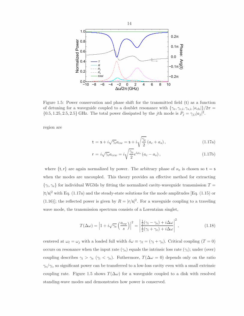
Figure 1.5: Power conservation and phase shift for the transmitted field (t) as a functionof detuning for a waveguide coupled to a doublet resonance with γe, γc,i, γs,i, |κcb|/2π =0.5, 1.25, 2.5, 2.5 GHz. The total power dissipated by the jth mode is Pj = γj,i|aj|2.
region are
t = s + i√γeacw = s + i
√
γe
2(ac + as) , (1.17a)
r = i√γeaccw = i
√
γe
2eiϕo (ac − as) , (1.17b)
where t, r are again normalized by power. The arbitrary phase of κe is chosen so t = s
when the modes are uncoupled. This theory provides an effective method for extracting
γi, γe for individual WGMs by fitting the normalized cavity-waveguide transmission T =
|t/s|2 with Eq. (1.17a) and the steady-state solutions for the mode amplitudes [Eq. (1.15) or
(1.16)]; the reflected power is given by R = |r/s|2. For a waveguide coupling to a traveling
wave mode, the transmission spectrum consists of a Lorentzian singlet,
T (∆ω) =∣
∣
∣1 + i
√γe
(acw
s
)∣
∣
∣
2=
∣
∣
∣
∣
∣
12(γi − γe) + i∆ω12(γi + γe) + i∆ω
∣
∣
∣
∣
∣
2
, (1.18)
centered at ωℓ = ωj with a loaded full width δω ≡ γℓ = (γi + γe). Critical coupling (T = 0)
occurs on resonance when the input rate (γe) equals the intrinsic loss rate (γi); under (over)
coupling describes γi > γe (γi < γe). Futhermore, T (∆ω = 0) depends only on the ratio
γe/γi, so significant power can be transferred to a low-loss cavity even with a small extrinsic
coupling rate. Figure 1.5 shows T (∆ω) for a waveguide coupled to a disk with resolved
standing-wave modes and demonstrates how power is conserved.
15
When |κcb| ≪ 12 (γi + γe), the coherent backscattering term can be ignored in the evolu-
tion of acw [Eq. (1.15a)] to first order. In this limit, the κcb dynamics become inconsequential
relative to the overall cavity decay. However, even weak backscattering will excite the accw
mode and produce a reflected field; the steady-state reflection spectrum from a mode with
weak Rayleigh scattering is
R(∆ω) =γ2e |κcb|2
∆ω2 +[
12 (γi + γe)
]22 . (1.19)
As expected the reflected power is very small, but it will be non-zero for all real WGM
resonators.
These coupled mode amplitudes accurately describe real resonators for a wide range of
γi and γe values as long as the system consists of a single waveguide mode and the paired
WGMs. The interference between two nearly degenerate cavity modes is frequently encoun-
tered when searching for high-neff TEp=1 modes with a fiber-taper. To help overcome the
phase mismatch, the taper is placed on the disk edge to increase the modal overlap. In this
position, T (∆ω) will display weak coupling to high-m low-γi modes, but it will also deeply
couple to broad high-p modes that are nearly phase matched to the waveguide resulting in a
Fano-like response [71]. These resonances require the source terms in Eqs. (1.15) and (1.16)
to account for the phase shift (Fig. 1.5) induced by other cavity modes [72, 73]. Since the
source field (s) is typically only an excitation of the waveguide’s fundamental eigenmode,
multiple waveguide modes effectively introduce a parasitic loss component (γp) in γi to
account for decay into the extra waveguide channels:
γ′i = γi + γp = γi +∑
k 6=1
γk,e, (1.20)
where γk,e is the extrinsic loss rate into the kth waveguide mode. The summation does not
include the pump mode (k = 1) because γ1,e is already explicitly included in Eq 1.15, and the
coupling coefficient for the source field remains κe = i√γe,1. Parasitic losses can significantly
broaden the transmission response of a WGM resonance for waveguides supporting higher
order transverse modes. To avoid parasitic loading, the waveguide should be small enough
to cut off all but the fundamental mode. The single-mode criteria for a tapered optical fiber
16
waveguide isrwg
λo<
2.405
2π√
n2wg − n2
o
, (1.21)
where rwg is the taper radius and nwg (no) is the refractive index of the waveguide (cladding),
which gives rwg < 0.56µm for λo = 1550 nm [49]; no similar geometric constraint exists for
partially etched ridge waveguides.9 The amount of parasitic coupling is described by the
junction’s ideality I = γe/(γe + γp) which is the ratio of the desired coupling over the
coupling to all modes of the waveguide; I ≥ 0.9997 has been observed for a fiber-taper
coupled to a microsphere cavity [75]. Parasitic loading is usually of little concern for high-
neff WGMs since the higher-order waveguide modes have lower neff than the fundamental
and worse phase mismatch with the WGMs.
Even for single-mode waveguides, a parasitic channel exists when coupling to a standing-
wave mode. Comparing Eqs. (1.15) and (1.16) after rotating to the ac, as basis, the
coefficient on the source field s is reduced (i√γe → i
√
γe/2 = i√
γ′e) as the waveguide feeds
ac and as equally, but the extrinsic loss term apparently remains the same. Because the
standing waves couple evenly to the waveguide’s forward- (+y) and backward-propagating
(–y) modes, the desired loading by the forward mode produces an extrinsic decay γ′e = γe,
and coupling to the backward mode produces parasitic decay at rate γp = γe/2. In this
case, I = 0.5, and γ′i + γ′e = γi + γe. By feeding the reflection channel, pure standing-
wave resonators (such as a Fabry-Perot cavity) can never over couple to a waveguide and
only asymptotically approach critical coupling as γ′e → ∞. For real WGM cavities, the
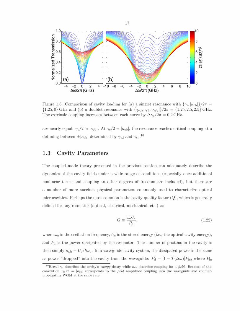
finite backscattering rate complicates the loaded transmission response (Fig. 1.6) since the
modes can contain both traveling- and standing-wave character. With |κcb| ≪ γi/2, T (∆ω)
for the traveling-wave mode follows Eq. (1.18), critically couples at ∆ω = 0 with γe =
γi, and overcouples at γe > γi when the waveguide mode becomes the cavity’s dominate
loss channel. When backscattering is significant, increased waveguide loading morphs the
doublet lineshape to a singlet as in Fig. 1.6(b). During this evolution, the waveguide
transmission resonant with the standing-wave modes (∆ω = ±|κcb|) never reaches zero, and
the resonance behaves like an overcoupled traveling-wave WGM when γe ≫ γc,i, γs,i, |κcb|.The transition between these two regimes occurs when the backscattering and extrinsic loss
9The single-mode condition generally attributed to R. A. Soref [74] for ridge waveguides in SOI onlyapplies for large cross-sectional areas and is not a cutoff condition. Higher-order transverse modes aresupported, but they leak out after propagating a short distance.
17
4
0.0
0.2
0.4
0.6
0.8
1.0
No
rma
lize
d T
ran
sm
issio
n
−10 −8 −6 −4 −2 0 2 4 6 8 10∆ω/2π (GHz)
6
0
2
8
10
γe /2
π (G
Hz)
−4 −2 0 2 4∆ω/2π (GHz)
(a) (b)
Figure 1.6: Comparison of cavity loading for (a) a singlet resonance with γi, |κcb|/2π =1.25, 0GHz and (b) a doublet resonance with γc,i, γs,i, |κcb|/2π = 1.25, 2.5, 2.5 GHz.The extrinsic coupling increases between each curve by ∆γe/2π = 0.2 GHz.
are nearly equal: γe/2 ≈ |κcb|. At γe/2 = |κcb|, the resonance reaches critical coupling at a
detuning between ±|κcb| determined by γc,i and γs,i.10
1.3 Cavity Parameters
The coupled mode theory presented in the previous section can adequately describe the
dynamics of the cavity fields under a wide range of conditions (especially once additional
nonlinear terms and coupling to other degrees of freedom are included), but there are
a number of more succinct physical parameters commonly used to characterize optical
microcavities. Perhaps the most common is the cavity quality factor (Q), which is generally
defined for any resonator (optical, electrical, mechanical, etc.) as
Q ≡ ωoUc
Pd, (1.22)
where ωo is the oscillation frequency, Uc is the stored energy (i.e., the optical cavity energy),
and Pd is the power dissipated by the resonator. The number of photons in the cavity is
then simply nph = Uc/ℏωo. In a waveguide-cavity system, the dissipated power is the same
as power “dropped” into the cavity from the waveguide: Pd = [1 − T (∆ω)]Pin, where Pin
10Recall γe describes the cavity’s energy decay while κcb describes coupling for a field. Because of thisconvention, γe/2 = |κcb| corresponds to the field amplitude coupling into the waveguide and counter-propagating WGM at the same rate.
18
is the input power in the waveguide. By simply depending on T (∆ω), the dissipated power
includes parasitic loss into the reflected channel but omits power coupled from the cavity
back into the transmitted channel—this portion is just “delayed.” Because Pd = −dUc/dt,
Eq. (1.22) can be recast as a differential equation solved by Uc(t) = Uc(0)e−ωot/Q, and the
cavity energy response in the time- and frequency-domain identify Q in terms of the cavity
photon lifetime (τph) and loaded cavity decay rate (γℓ),
Q = ωoτph =ω
γℓ, (1.23)
where τph is a “linear” time if ωo is an “angular” frequency. As before, γℓ includes all
loss mechanisms (γi + γe + γp) and is the full width at half maximum of Uc(ω). The
cavity’s intrinsic Qi is determined by the cavity’s inherent loss mechanisms independent
of the waveguide (Qi = ω/γi), whereas Eq. (1.23) is conventionally labelled the loaded
Qℓ. Because Q is a dimensionless quantity, it is often partitioned among the various loss
mechanisms rather than separating γℓ. For examples, Qss = ωo/γss would be the cavity Q
if surface scattering were entirely responsible for the decay of Uc(t). Since the loss rates are
additive, the components of Qi add reciprocally:
1
Qi=
1
Qrad+
1
Qss+
1
Qa+ . . . , (1.24)
where the summation does not include Qe or Qp, which are associated with extrinsic cou-
pling to the desired and parasitic waveguide modes, respectively.
While Q, τph, γℓ quantify how long the photons remain in the cavity, the phase and
group velocities are necessary to establish how they circulate around the resonator. Un-
fortunately, the linear propagation constant (β) is not rigorously defined because it varies
with radius—converting the angular propagation to Cartesian coordinates gives: e±imϕ ≈e±imx/r. Since the phase velocity (vp) tangent to the disk edge can vary with radius (r), it
can be found according to its usual definition
vp ≡ ω
β=ωor
m. (1.25)
More care must be taken with the linear group velocity (vg), which is the velocity of the
spatially extended optical wave packet. The group velocity is approximately constant across
19
the WGM for all but the smallest microdisks and is given by
vg ≡ ∂ω
∂β≈ ωm+1 − ωm
m+1Ravg
− mRavg
,= δωfsrRavg (1.26)
where δωfsr is the free spectral range (FSR) between two adjacent modes in the same
family and Ravg is the average radius of the mode’s energy density; the group index is then
ng ≡ c/vg = c/(δωfsrRavg). For the p = 1 WGMs studied in this work, Ravg is nearly
equal to the disk’s radius. The group velocity is particularly important when dealing with
loss (α) or gain coefficients expressed as an inverse length. The processes producing the
loss/gain occur in the time domain and are analyzed using transition rates (e.g., Fermi’s
Golden Rule). These rates are then converted to an inverse length using the group velocity
(e.g., by considering how long it takes for a pulse to traverse an absorbing region of fixed
length) rather than the phase velocity. While free-space optical studies in bulk materials
may be weakly dispersive, the guided waves in microphotonics can experience significant and
dynamic modal dispersion (e.g., Ref. [76]). For this reason, the various optical processes
will be mainly described using rates (γx as in §1.2), and they will only be converted to
inverse lengths for comparison to published sources: αx = γx/vg.
The group velocity can be used to find several other quantities. The effective interaction
length (Leff) is the mean distance a photon will travel in the cavity before it escapes and
is given by: Leff = vgτph. For a low-loss micron-scale resonator, Leff can easily be >1 cm—
demonstrating why microcavies are sensitive to small perturbations. The round-trip time
for a photon to circle the cavity is τrt = 2πRavg/vg ≈ 2π/δωfsr, and the number of round
trips a photon makes is τph/τrt ≈ δωfsr/(2πγℓ) = F/2π where F ≡ δωfsr/γℓ ≈ Q/m is the
cavity’s finesse. These relations then relate the dropped power to the power circulating in
the WGM (Pcir = FPd/2π), which can exceed 10 W when the cavity is pumped continuous
wave (CW) or pulsed (pulse width & 3τph) with 1 mW from an external waveguide.
Depending on the application, the strength (per photon) and distribution of the cavity
fields are often significant. In cavity quantum electrodynamics (cQED), the electric field
strength per photon is
| ~E| =
√
ℏω
2n2ǫoVeff, (1.27)

20
where Veff is the effective mode volume given by
Veff =
∫
n2(~r)| ~E(~r)|2dVmax
[
n2(~r)| ~E(~r)|2] . (1.28)
This mode volume can be found using the FEM and roughly corresponds to the volume
occupied optical fields. While Veff generally scales with the cavity size, this behavior can be
misleading for slotted structures [18]. Other definitions of Veff exist for nonlinear processes
that employ higher moments of the field (e.g., Refs. [62, 77]), but Eq. (1.28) will be used
throughout this thesis unless otherwise noted. In many hybrid photonic structures, the
fraction of the optical mode’s energy in a given volume (δV ) or on a surface (δA) is more
important than Veff . For example, a hybrid microcavity laser consisting of an active layer
stacked on a passive waveguide layer can exhibit significantly lower gain if the optical mode
largely contained in the passive material. The volumetric overlap factor can be calculated
with the FEM using
Γ =
∫
δV n2(~r)| ~E(~r)|2dV
∫
n2(~r)| ~E(~r)|2dV, (1.29)
and a similar areal overlap is defined as
Γ′ =
∫
δA n2(~r)| ~E(~r)|2dA
∫
n2(~r)| ~E(~r)|2dV, (1.30)
where both denominators are integrated over all space. The Γ′ factors are commonly used
when analyzing issues of surface sensitivity (sensing, absorption by surface states, etc.), and
they can be converted to a volumetric energy fraction by assuming the surface has some
effective interaction depth (d′): Γ = Γ′d′.
21
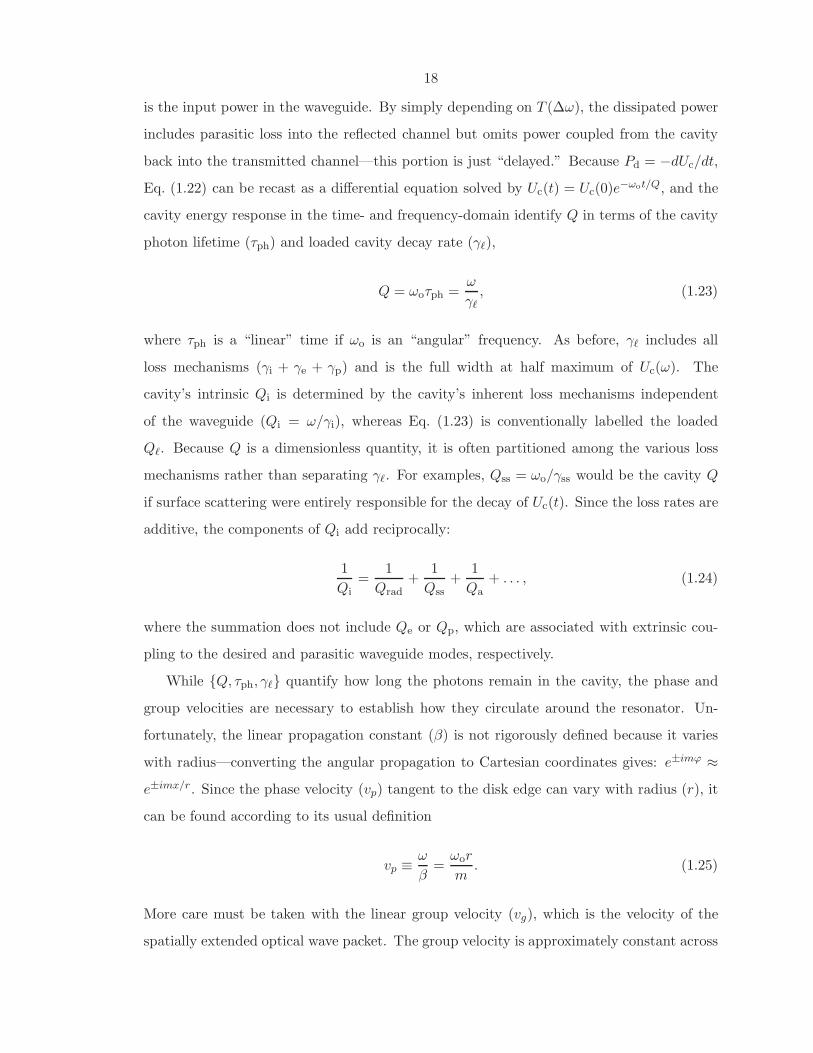
Chapter 2
“Dimpled” Fiber-Taper Probe
In microelectronics manufacturing, nondestructive parametric testing using metal probe
tips greatly increases fabrication yield through statistical process control [78]. For test-
ing of glass and semiconductor photonic lightwave circuits (PLCs), many methods exist
for the coupling of light into and out of on-chip waveguides [79]. However, no simple,
local probe exists for wafer-scale, nondestructive, optical characterization of on-chip com-
ponents. Traditional optical coupling methods include end-fire or butt coupling [80–82] and
prism-based coupling [83, 84]. End-fire coupling from free-space or optical fibers can be
made highly efficient, even to high-index contrast semiconductor waveguides, through the
use of tapered waveguide sections [80–82] or other non-adiabatic mode converters [85, 86],
but they are limited to coupling at the periphery of the chip where a cleaved facet can be
formed. Evanescent-coupling methods involving conventional prism couplers, angled-fiber
tip couplers [87], eroded-fiber couplers [88], and optical fiber-tapers [89–91] can provide
effective coupling to and from on-chip waveguides, but these probes are less suited to wafer-
scale coupling to micron-scale photonic elements due to their macroscopic extent in one
or both in-plane dimensions. Evanescent coupling techniques also rely on phase matching
to obtain highly efficient coupling [70, 75, 77, 92], which can be difficult (although not im-
possible [77, 93]) to satisfy for semiconductor-based microphotonic chips. Other methods
of coupling light onto photonic chips for characterization purposes involve dedicated on-
chip testing structures such as in-plane grating couplers [94]. These couplers typically also
involve specialized processing to achieve high coupling efficiency: blazed gratings [95], a
combination of lateral and vertical Bragg reflectors [96], or additional overlayers [97].
We present a variant of the silica optical fiber-taper evanescent-coupler that is designed
for rapid, wafer-scale diagnostic testing of on-chip photonic components such as waveguides
22
and resonant filters. Previous work involving straight fiber-tapers required devices to be
elevated by several microns above the chip surface to prevent parasitic coupling to the
surrounding substrate. Curved fiber-taper probes [92, 98–101] have been demonstrated
to reduce parasitic loss into the substrate. However, they tend to be less mechanically
stable than their tensioned straight-taper counterparts and suffer from noise induced by
fluctuations in the taper’s position. In this work we have developed a microscopic “dimpled”
fiber-taper probe which allows for low-noise local probing of individual devices on a wafer.
By increasing the tension in the taper, fluctuations in the taper-chip gap can be greatly
reduced to the levels present in straight fiber-taper measurements. To demonstrate the
utility of the dimpled taper optical probe, we describe the characterization of two types of
devices on a SOI wafer platform: a dense two-dimensional array of high-Q silicon microdisk
resonators and, second, a planar microring resonator.
2.1 Taper Pulling and Molding
The dimpled fiber-taper probe is made from a standard straight fiber-taper that is pressed
against a mold and heated (Fig. 2.1). We form “straight” fiber-tapers by simultaneously
heating and pulling standard telecommunication fiber (specifically Corning SMF-28e and
NuFern 1060-XP) using two linear motorized stages and a hydrogen torch. The fiber is
positioned at the edge of the flame so only a small portion of the fiber is heated; larger
hot zones produce long pliable tapers that are more difficult to mount. The diameter of
the taper is constantly monitored during the pull by either watching the fiber’s mechanical
deflection in the flame or by measuring the fiber’s transmission at the desired wavelength.
In the final single-mode taper coupler, the fundamental core-guided HE11 fiber mode is adi-
abatically converted by slowly thinning the fiber to the HE11 taper mode with evanescent
tails that extend significantly into the surrounding medium. However at larger diameters
while it is being drawn, the optical field in the tapering region is a superposition of the
LPmn modes [102]. As the diameter is reduced, the higher-order components are reflected
producing an oscillating signal with a frequency that increases as the pull progresses. When
the fiber approaches the diameter that cuts off all higher order modes, the transmission os-
cillations abruptly cease [Fig. 2.1(b)]. A running standard deviation of this signal (sampling
at 100 kHz and analyzing a circular buffer at 5Hz) exhibits a sharp drop that can be used
23
(c) (d)
DimpleStraight taper
Straighttaper
Pull Down
Fiber mold
Hot zone
around the moldU-Mount with adjustable tension
High tension
Low tension
Dimple is shallower with less mechanical noise
Dimple is deeper with more mechanical noise
(e)Tapered fiber pulled
Heating torch
-- On
Heating torch
-- Off
Separate to increase
tension
Heating torch
-- On
Pull
Pull
Hot zone at
edge of flame
(a) (b)
0 25 50 75 100 125 150
Time (s)
Norm
. T
rans.
1.00
0.90
0.80
0.70
Runnin
gS
td. D
ev.
(%
)
0
1
2
3
4
5
61060XP fiber
SMF28e fiber
single
mode
Figure 2.1: Process for producing dimpled fiber-taper probes. (a) Taper pulling with thefiber placed at the edge of the flame to produce a small hot zone. (b) Characteristic in situdown-sampled transmission traces for 1060-XP and SMF-28e fiber during a taper pull. Therunning standard deviation for these traces shows the onset of single-mode behavior. (c)Forming the dimple by heating taper while it is pressed against a mold fiber. (d) Detachingthe probe from the mold. (e) Schematic of a U-mount with variable tension.
24
to trigger the end of the pull.1 To produce tapers with the desired length (∼1 cm for the
region with d . 10µm) and minimum diameter (∼1µm), typical pulls continue ∼10 s after
the oscillations stop and take 120–150 s with the stages each moving at ∼1.5 cm/min, but
there is significant variability depending on how the fiber is prepared. For instance, the
single-mode jump in the running standard deviation will contain one or more discrete steps
if the fiber is subjected to undue stress while the polymer coating is being removed.
After mounting the taper in a U-bracket [104], the narrowest part of the taper is pressed
against a silica mold with the desired radius of curvature [Fig. 2.1(c)]; a bare optical fiber
with a diameter of approximately 125 µm is used as the mold in these experiments. The
taper and mold are heated with a hydrogen torch and allowed to cool. To detach the taper
from the mold, we simply pull the taper away slowly while moving it back and forth (i.e.,
we are inducing fatigue failure at the taper-mold joint). A thin layer of soot on the mold
improves the detachment yield—an appropriate layer is usually deposited when the torch
is sparked.2 After releasing the fiber from the mold, the taper retains an impression of
the mold, Fig 2.2(b), which forms a global minimum with respect to the rest of the taper.
The dimpling process introduces negligible additional loss, and the total loss of the dimpled
taper can be less than 0.5 dB relative to the unpulled optical fiber. However, tapers typically
exhibit a total loss 1–2 dB. Using a specially designed U-mount with a set screw to control
the tensioning, varying the taper’s tension changes the radius of curvature of the dimple.
Under high tension, the dimple becomes very shallow but never completely straightens.
After dimpling, the probe is mounted onto a three-axis 50-nm encoded stage and is fusion
spliced into a versatile fiber-optic setup. During testing, devices are placed in the near field
of the probe, as in Fig. 2.2(a,c); adjustments to a pair of goniometers ensure the straight
run of the taper is parallel to the sample surface.
Measurement of the non-resonant insertion loss as the waveguide is moved relative to
nearby semiconductor microstructures gives the effective interaction length and profile of
the local probe. First, we record the loss as a 1.6-µm wide GaAs cantilever is scanned along
the taper’s length (x-direction) while holding the taper at a fixed height. At tensions used in
standard testing, Fig. 2.3(a) shows only ∼20µm (full width at half maximum) of the taper
1This method was implemented by C. Chrystal. A similar procedure has been published by F. Orucevicet al. using a running Fourier transform [103].
2N.B. Do not spark H2 torches near the fiber either before or after tapering as it will significantly reducethe transmission of the final coupler.
25
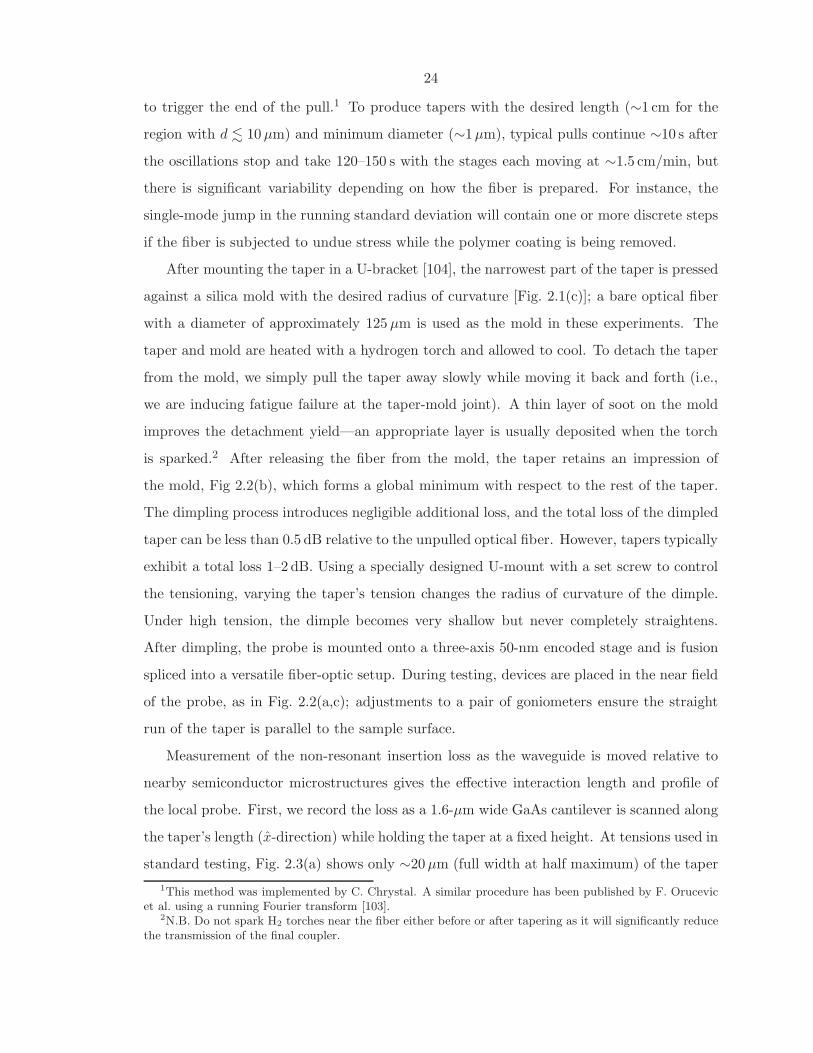
5 μm
50 μ
m
20 μm
Figure 2.2: (a) Illustration of a “dimpled” taper coupled to an undercut microdisk. (b)Optical image of the taper probe. The taper diameter at the center of the dimple is ∼1.2µm.(c) At the center of a 5×5 array, the dimpled taper probe is critically coupled to themicrodisk at the center of the array but not coupled to any of the neighboring disks.
at the bottom of the dimple is close enough to interact with the sample. Second, the loss
is measured as a function of the probe’s height (z-direction) above a 11.6-µm wide GaAs
mesa. By assuming an exponential vertical dependence for the insertion loss L ∝ e−zt(x)/zo
where zt(x) is the probe’s “near-field” profile and zo is the decay length from Fig. 2.3(b),
we convert the axial dependence of the loss [Fig. 2.3(a)] into zt(x) [Fig. 2.3(c)]—i.e., the
height of the taper relative to the lowest point of the dimple. Since only the lowest part
of the dimple interacts with the sample, this method can only determine the taper’s profile
within ∼1.25µm of the surface. Fitting the profiles determines the effective probe radius to
be 159, 228, and 498 µm at low, medium, and high tension, respectively. These radii differ
from the mold radius (∼62µm) due to tensioning of the taper and how the fiber detaches
from the mold after heating.
2.2 Microphotonic Testing with a Dimple-Taper Waveguide
To study microresonators with a dimpled probe and the general arrangement in Fig. 2.4, pre-
cision stages are used to move the waveguide into the device’s near field giving controllable
and reproducible coupling. Isolating the measurements from stray air currents is imperative,
and all testing is conducted in a continuously N2-purged enclosure. The N2 environment
also extends the probe’s lifetime since fiber-tapers are hygroscopic and can suffer significant

26
-60 -40 -20 0 20 400.0
0.2
0.4
0.6
0.8
1.0Loss (
arb
. lin
ear
units)
Axial Position: x (µm)
0 0.5 1.0 1.5
Transverse Postion: z (µm)
-60 -40 -20 0 20 40 600.0
0.5
1.0
1.5
2.0
Axial Position: x (µm)
Pro
file
: z
t(x)
(µm
)Medium TensionLow Tension
High Tension
a) b)
c)
Loss ∝ exp(-z/ zo)
zo = 0.34 µm
zx
xz
Figure 2.3: Non-resonant insertion loss (a) as a function of axial position (x) as a narrowcantilever is moved along the taper length and (b) as a function of transverse position (z)as the dimple is raised above a mesa. (c) Inferred dimple taper profile at “low,” “medium,”and “high” tension.
1420-1495 nm
Tunable Laser
1495-1565 nm
Tunable Laser
1565-1625 nm
Tunable LaserDisk
TaperPD
Trans
PDRef
10%
10 : 90splitter
N2 Purge BoxVOA FPC
10 : 90splitter
MZ I
PDNorm
VOA
10%
Figure 2.4: Basic arrangement for microcavity transmission measurements. An ancillarynormalization detector can be used to remove the oscillations produced by the residualetalon between the laser diode’s facets. A fourth laser (spanning 1480–1580 nm) is usedto study any resonances at the boundaries of the primary lasers’ sweep ranges (i.e., near1495 and 1565 nm). Abbreviations: variable optical attenuator (VOA), fiber polarizationcontroller (FPC), Mach-Zehnder interferometer (MZI), and photodiode (PD).

27
losses by absorption at the first overtone of the OH− vibrational modes [105, 106].3 The
HE11 mode of the taper is excited using fiber-coupled swept tunable-laser sources (span-
ning 963–993 nm and 1420–1625 nm, linewidth of <300 kHz over the 25-ms timescale used
to scan across a high-Q resonance) and a paddle-wheel polarization controller to selectively
couple to the cavity’s TE-like and TM-like WGMs. To accurately measure the intrinsic
quality factor, the cavities are weakly loaded by the dimpled probe to ensure the extrinsic
loading is negligible (γe ≈ 0) and avoid any parasitic coupling. Two complementary VOAs
are used to maintain a constant optical power at the photodetector (to give a constant
electronic noise level) while power at the device can be varied up to 60 dB [107]. To elimi-
nate any nonlinear effects or absorption saturation while acquiring the transmission spectra,
the lasers are usually attenuated to give ∼200 nW at the taper, of which ∼10% is coupled
into the microdisk cavity. Without any optical amplification, the signal is detected using a
high-speed InGaAs photodiode, electrically amplified using a low-noise analog preamplifier,
and then is aquired by a analog-to-digital converter. For narrow spectral features (e.g.,
Q > 106 corresponds to δλ . 1.5 pm), the linewidth measurement can be calibrated with a
fiber-optic Mach-Zehnder interferometer to an accuracy of ±0.02% (see also §A.1).
2.2.1 Noise Measurements
Because evanescent coupling to fiber-tapers is exponentially dependent on position, fiber-
taper measurements are very susceptible to any noise sources that produce physical dis-
placements of the taper. For straight tapers, increasing tension to reduce these fluctuations
is common, and the U-mount [104] naturally provides the appropriate tautness. Under
standard testing conditions at low dimple-taper tension [Fig. 2.5(a)], coupling to the mode
of a microdisk resonator [see Fig. 2.2(a) and §2.2.2] varies significantly between consecu-
tive scans. Increasing the tension makes the coupling depth much more reproducible, as in
Fig. 2.5(b). At tensions that give acceptable noise levels, the depth of the dimple is still
adequate for testing densely spaced planar devices.
To quantitatively study the noise, we measure non-resonant insertion loss as a function
of time. The dimple is placed above the etched GaAs mesa so that approximately 60%
of the incident power is coupled into the substrate [z ≈ 170 nm as in Fig. 2.3(b)]. The
3After months of use in a N2 box, enough water and dust will accumulate to significantly reduce thetaper’s transmission. Often this loss can be partially ameliorated by dipping the taper in trichloroethylene(TCE).
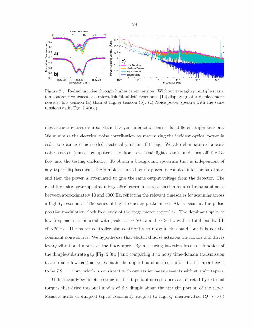
28
0.6
0.7
0.8
0.9
1562.31 1562.33 1562.35
0.7
0.8
0.9
Wavelength (nm)
Norm
aliz
ed T
ransm
issio
n
10 -1
Frequency (Hz)
Pow
er
Spectr
al D
ensity (
V2/H
z)
10 0 10
1 10 2 10
3 10 4
10 -4
10 -6
10 -8
10 -10
10 -12
10 -14
Low Tension
Medium Tension
High Tension
Background
Scan Time (ms)
0
0.6
5 10 15 20 25
a)
b)
c)
Figure 2.5: Reducing noise through higher taper tension. Without averaging multiple scans,ten consecutive traces of a microdisk “doublet” resonance [42] display greater displacementnoise at low tension (a) than at higher tension (b). (c) Noise power spectra with the sametensions as in Fig. 2.3(a,c).
mesa structure assures a constant 11.6-µm interaction length for different taper tensions.
We minimize the electrical noise contribution by maximizing the incident optical power in
order to decrease the needed electrical gain and filtering. We also eliminate extraneous
noise sources (unused computers, monitors, overhead lights, etc.) and turn off the N2
flow into the testing enclosure. To obtain a background spectrum that is independent of
any taper displacement, the dimple is raised so no power is coupled into the substrate,
and then the power is attenuated to give the same output voltage from the detector. The
resulting noise power spectra in Fig. 2.5(c) reveal increased tension reduces broadband noise
between approximately 10 and 1000 Hz, reflecting the relevant timescales for scanning across
a high-Q resonance. The series of high-frequency peaks at ∼15.8 kHz occur at the pulse-
position-modulation clock frequency of the stage motor controller. The dominant spike at
low frequencies is bimodal with peaks at ∼120 Hz and ∼130 Hz with a total bandwidth
of ∼20 Hz. The motor controller also contributes to noise in this band, but it is not the
dominant noise source. We hypothesize that electrical noise actuates the motors and drives
low-Q vibrational modes of the fiber-taper. By measuring insertion loss as a function of
the dimple-substrate gap [Fig. 2.3(b)] and comparing it to noisy time-domain transmission
traces under low tension, we estimate the upper bound on fluctuations in the taper height
to be 7.9 ± 1.4 nm, which is consistent with our earlier measurements with straight tapers.
Unlike axially symmetric straight fiber-tapers, dimpled tapers are affected by external
torques that drive torsional modes of the dimple about the straight portion of the taper.
Measurements of dimpled tapers resonantly coupled to high-Q microcavities (Q ≈ 106)
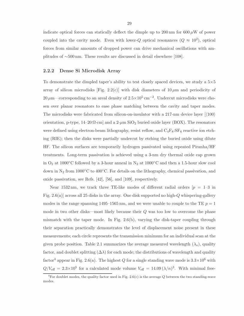
29
indicate optical forces can statically deflect the dimple up to 200 nm for 600 µW of power
coupled into the cavity mode. Even with lower-Q optical resonances (Q ≈ 102), optical
forces from similar amounts of dropped power can drive mechanical oscillations with am-
plitudes of ∼500 nm. These results are discussed in detail elsewhere [108].
2.2.2 Dense Si Microdisk Array
To demonstrate the dimpled taper’s ability to test closely spaced devices, we study a 5×5
array of silicon microdisks [Fig. 2.2(c)] with disk diameters of 10µm and periodicity of
20µm—corresponding to an areal density of 2.5×105 cm−2. Undercut microdisks were cho-
sen over planar resonators to ease phase matching between the cavity and taper modes.
The microdisks were fabricated from silicon-on-insulator with a 217-nm device layer [〈100〉orientation, p-type, 14–20 Ω·cm] and a 2-µm SiO2 buried oxide layer (BOX). The resonators
were defined using electron-beam lithography, resist reflow, and C4F8:SF6 reactive ion etch-
ing (RIE); then the disks were partially undercut by etching the buried oxide using dilute
HF. The silicon surfaces are temporarily hydrogen passivated using repeated Piranha/HF
treatments. Long-term passivation is achieved using a 3-nm dry thermal oxide cap grown
in O2 at 1000C followed by a 3-hour anneal in N2 at 1000C and then a 1.5-hour slow cool
down in N2 from 1000C to 400C. For details on the lithography, chemical passivation, and
oxide passivation, see Refs. [42], [56], and [109], respectively.
Near 1532 nm, we track three TE-like modes of different radial orders [p = 1–3 in
Fig. 2.6(a)] across all 25 disks in the array. One disk supported no high-Q whispering-gallery
modes in the range spanning 1495–1565 nm, and we were unable to couple to the TE p = 1
mode in two other disks—most likely because their Q was too low to overcome the phase
mismatch with the taper mode. In Fig. 2.6(b), varying the disk-taper coupling through
their separation practically demonstrates the level of displacement noise present in these
measurements; each circle represents the transmission minimum for an individual scan at the
given probe position. Table 2.1 summarizes the average measured wavelength (λo), quality
factor, and doublet splitting (∆λ) for each mode; the distributions of wavelength and quality
factor4 appear in Fig. 2.6(a). The highest Q for a single standing wave mode is 3.3×10⁶ with
Q/Veff = 2.3×10⁵ for a calculated mode volume Veff = 14.09 (λ/n)3. With minimal free-
4For doublet modes, the quality factor used in Fig. 2.6(c) is the average Q between the two standing-wavemodes.
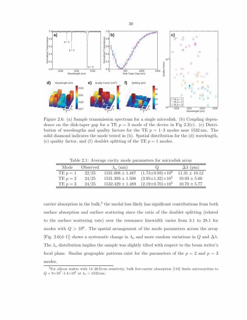
30
0
10
20
30
40
0
1
2
3
1527
1529
1531
1533
0 500 1000 15000.0
0.2
0.4
0.6
0.8
1.0
Disk-Taper Gap (nm)
Norm
aliz
ed T
ransm
issio
n
1530 1531 15320.0
0.2
0.4
0.6
0.8
1.0
Wavelength (nm)
Norm
aliz
ed T
ransm
issio
n
p = 1
p = 2
p = 3
1529 1531 1533 1535
10 6
Wavelength (nm)
Qualit
y F
acto
r
TE p = 1 TE p = 2TE p = 3
10 5
c)a) b)
d) e) f)Wavelength (nm) Quality Factor (x10
6) Splitting (pm)
yx
yx
yx
Figure 2.6: (a) Sample transmission spectrum for a single microdisk. (b) Coupling depen-dence on the disk-taper gap for a TE p = 3 mode of the device in Fig 2.2(c). (c) Distri-bution of wavelengths and quality factors for the TE p = 1–3 modes near 1532 nm. Thesolid diamond indicates the mode tested in (b). Spatial distribution for the (d) wavelength,(e) quality factor, and (f) doublet splitting of the TE p = 1 modes.
Table 2.1: Average cavity mode parameters for microdisk array
Mode Observed λo (nm) Q ∆λ (pm)
TE p = 1 22/25 1531.008 ± 1.487 (1.73±0.93)×106 11.31 ± 10.12TE p = 2 24/25 1531.393 ± 1.508 (3.95±1.32)×105 10.93 ± 5.60TE p = 3 24/25 1532.429 ± 1.489 (2.19±0.70)×105 10.70 ± 5.77
carrier absorption in the bulk,5 the modal loss likely has significant contributions from both
surface absorption and surface scattering since the ratio of the doublet splitting (related
to the surface scattering rate) over the resonance linewidth varies from 3.1 to 28.1 for
modes with Q > 106. The spatial arrangement of the mode parameters across the array
[Fig. 2.6(d–f)] shows a systematic change in λo and more random variations in Q and ∆λ.
The λo distribution implies the sample was slightly tilted with respect to the beam writer’s
focal plane. Similar geographic patterns exist for the parameters of the p = 2 and p = 3
modes.
5For silicon wafers with 14–20 Ω·cm resistivity, bulk free-carrier absorption [110] limits microcavities toQ < 9×10⁷–1.4×10⁸ at λo = 1532 nm.
31
-4 -3 -2 -1 0 1 2 3 4
0.980
0.984
0.988
0.992
0.996
1.000
Wavelength (pm)
Norm
aliz
ed T
ransm
issio
n
δλ = 0.35 pmδλ = 0.30 pma)
b)c)
Q = 4.1x10⁶
Q = 4.8x10620 μm
200 nm
Figure 2.7: SEM images of rings after the final chemical treatments and 30-nm thermaloxidation: (a) top-view of a ring with a 20-µm diameter and 2-µm width and (b) sideview showing smooth ring sidewalls and a slight BOX undercut due to the final chemicaltreatments. (c) Transmission spectrum of a high-Q mode at λo = 1428.7 nm in a ring withan 80-µm diameter and a 2-µm width.
2.2.3 Planar Si-SiO2 Microring via RIE Processing
Testing planar devices is accomplished in the same fashion. Non-undercut microring res-
onators, shown in Fig. 2.7(a), were fabricated from SOI with a 195-nm silicon device layer
and a 3-µm BOX. The same lithography, resist reflow, and RIE procedure used for the
microdisks [42] was used to define the microrings although without the final HF undercut.
Repeated Piranha oxidations and HF dips are again used to chemically passivate the sur-
faces prior to thermal oxidation [56]; these treatments also slightly undercut the resonators
[Fig. 2.7(b)]. Finally, a 30-nm dry thermal oxide was grown as a capping layer, and the
microring sample was annealed according to the same N2 schedule as the microdisks [109].
Microrings are slightly more difficult to test with fiber-tapers than undercut microdisks.
A large phase mismatch exists between the taper and microcavity because of the extra
dielectric beneath the Si-core guided modes. With the taper in contact with the ring, the
coupling depth is more than sufficient to assess the devices’ optical loss characteristics.
However, the coupling is not adequate to efficiently excite and collect emission from active
devices [70]. For applications requiring high pump/collection efficiency, photonic crystal
waveguides can be used to overcome the poor phase matching between the modes in the
taper and the modes in the on-chip device [77].
Figure 2.7(c) shows a transmission spectrum of a ring with an 80-µm diameter and 2-
µm width after the final chemical treatments and thermal oxidation. The measured quality
32
factor of 4.8×10⁶ (loss coefficient α < 0.15 dB/cm) represents the highest quality factor
for any planar microresonator to date. Reproducing Qs found previously only in relatively
thick and undercut silicon disks [42] is promising for the future development of PLCs with
high-Q silicon microresonators integrated with bus waveguides.
2.2.4 Planar Si-SiO2 Microring via LOCOS Processing
Wet chemical oxidation of ridge waveguides has been used to smooth silicon surfaces and
reduce Rayleigh scattering [111]. However, similar treatments of high-Q microdisks did not
reduce the scattering rate but rather increased the measurable loss by introducing unpas-
sivated mid-gap surface states [56]. As evident by the contradictory results for chemical
oxides, significant care must be taken in low-loss fabrication procedures. Dry reactive-
ion chemistries are generally preferred over wet chemical etchants because they are more
anisotropic, but RIE recipes must be carefully optimized for roughness and can damage
the surface (chemically and physically). Two alternatives have been to use shallow rib
waveguides, in which the modes are weakly guided and have minimal overlap with the sur-
faces [112], or to use a diffusion-limited chemical reaction to produce the cladding layer [113].
In the latter case, dry thermal oxidation of Si device layer in SOI produces a low-loss SiO2
cladding with a well-passivated interface [109] and high refractive index contrast to the
underlying Si core. This section describes initial results for the fabrication and dispersion
engineering of submicron waveguides formed by the local oxidation of silicon (LOCOS).
With the ultimate objective of achieving CW parametric oscillation in a Si microcavity,
the final devices must be high Q, have a small group velocity dispersion (GVD) with a
zero-dispersion wavelength (ZDWL) near the desired wavelength, and exhibit a low free-
carrier lifetime (τfc). Degenerate four-wave mixing can be used to generate broadband gain
in silicon microphotonics because of its large χ3 nonlinearity [114], but the modal dispersion
must be controlled to ensure phase matching. In WGM resonators, the phase matching is
trivially satisfied between consecutive modes in a single family, but the GVD must be near
zero to converse energy (i.e., the signal and idler modes must be equally spaced about the
pump mode) [115]. An additional constraint when operating with a photon energy above
half the material’s bandgap is that τfc must be short to minimize absorption by e−/h+ pairs
generated by two-photon excitation.
The primary design goals for these initial devices are 1) nwgeff ≈ 2.0 so losses can rapidly
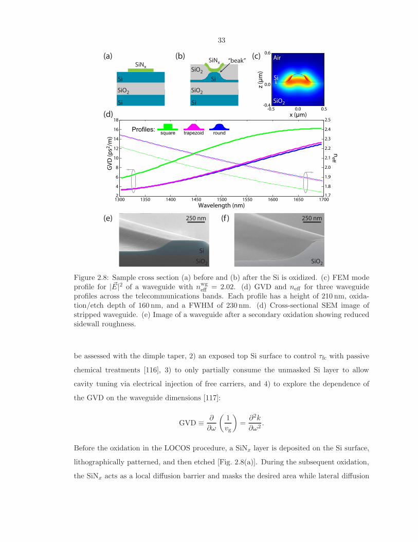
33
(a)
Si
Si
SiO2
SiNx
(b)“beak”SiNx
SiO2
Si
SiO2
Si
(e) (f )250 nm
Si
SiO2
250 nm
SiO2
0.0-0.5 0.5-0.4
0.0
0.6
x (μm)
z (μ
m)
(c)
1300 1350 1400 1450 1500 1550 1600 1650 1700
Wavelength (nm)
2
4
6
8
10
12
14
16
18
GV
D (
ps2
/m)
(d)
1.7
1.8
1.9
2.0
2.1
2.2
2.3
2.4
2.5
ne
ff
Profiles:square trapezoid round
SiO2
Si
Air
Figure 2.8: Sample cross section (a) before and (b) after the Si is oxidized. (c) FEM modeprofile for | ~E|2 of a waveguide with nwg
eff = 2.02. (d) GVD and neff for three waveguideprofiles across the telecommunications bands. Each profile has a height of 210 nm, oxida-tion/etch depth of 160 nm, and a FWHM of 230 nm. (d) Cross-sectional SEM image ofstripped waveguide. (e) Image of a waveguide after a secondary oxidation showing reducedsidewall roughness.
be assessed with the dimple taper, 2) an exposed top Si surface to control τfc with passive
chemical treatments [116], 3) to only partially consume the unmasked Si layer to allow
cavity tuning via electrical injection of free carriers, and 4) to explore the dependence of
the GVD on the waveguide dimensions [117]:
GVD ≡ ∂
∂ω
(
1
vg
)
=∂2k
∂ω2.
Before the oxidation in the LOCOS procedure, a SiNx layer is deposited on the Si surface,
lithographically patterned, and then etched [Fig. 2.8(a)]. During the subsequent oxidation,
the SiNx acts as a local diffusion barrier and masks the desired area while lateral diffusion
34
rounds the Si profile at the edges [Fig. 2.8(b)]. Since the resulting “bird beak” contour may
not be accurately captured by effective-index methods, the waveguide modes and disper-
sion are evaluated using the FEM. The effective-index requirement limits the geometries to
submicron dimensions that cut off all but the TEp=1 mode [Fig. 2.8(c)]—TM modes will
be avoided initially because of lateral leakage into the partially thinned slab [26]. Prelimi-
nary simulations show the dispersion can be flattened by modifying the waveguide profile
[Fig. 2.8(d)], but the GVD for modes with these dimensions may never reach zero in the
telecommunications windows. Smaller Si structures having greater overlap with the BOX
or a SiO2 cap will have a lower GVD because silica is anomalous in this range. To proceed,
we target a waveguide width of 230 nm, Si thickness of 210 nm, and a ridge height of 160 nm
with nwgeff = 2.02 at λo = 1550 nm. While ring resonators with these dimensions have sig-
nificant +GVD at 1550 nm, they are an acceptable starting point for process development.
Future devices may utilize the TMp=1 modes to simultaneously achieve the neff and GVD
objectives while demanding greater pattern control (i.e., waveguide width).
The process begins by using Piranha etch (3:1 concentrated H2SO4 to 30% H2O2) to
remove any residual organics on a SOI wafer (217 nm Si, 2µm BOX). After a quick HF
rinse to strip the native oxide, a 10-nm dry thermal oxide is grown at 1000C to serve as an
etch-stop layer and protect the Si surface. A 75-nm low-stress SiNx mask is then deposited
by plasma-enhanced chemical vapor deposition (PECVD). This layer must be thick enough
to provide an adequate diffusion barrier, but it must be compliant (thin) enough to not
delaminate as the SiO2 expands [Fig. 2.8(b)]. The nitride is then patterned with electron-
beam lithography, resist reflow, and RIE (C4F8:SF6). Since the selectivity between SiNx
and SiO2 is poor, the etch must be carefully timed to stop at the etch-stop layer. Following
another Piranha clean to take off any remaining resist and etch by-products, the sample is
oxidized in dry O2 (electronic grade II) at 1100C to define the waveguides. The SiO2 and
SiNx are then removed with HF leaving the Si surface bare for future surface treatments.
Initial results show reasonable smoothness for the waveguide sidewalls in Fig. 2.8(e), but
there is significant room for improvement throughout the fabrication flow. Since the exact
process conditions vary between SiNx etches (rate ≈ 1.5 nm/s), it is difficult to consistently
halt the RIE before penetrating the SiO2 layer. Rather than adjusting the etch recipe,
which should be optimized for roughness, the initial SiO2 thickness should be increased
even though this increases the duration of the LOCOS step. Second, the written waveguide
35
dimensions must be calibrated against the resulting widths to account for the resist reflow
and SiNx sidewall angle, which is not perfectly vertical. Even after correcting for lateral
diffusion that will undercut the SiNx by the same depth the sample is oxidized (e.g., oxidizing
down 160 nm to define a 230-nm waveguide requires a mask width of ∼550 nm), the final
waveguides were too large (∼500 nm) for testing with a dimple taper. Third, the long
LOCOS oxidation anneals the PECVD SiNx and increases its resistance to HF. Instead
of being etched during the final HF strip, the SiNx lifts off in one large sheet as the thin
SiO2 etch-stop is slowly undercut. Much of surface roughness on top of the waveguides is
likely due to the SiNx gradually pealing off the Si. In addition, the longer etch allows HF
to penetrate defects in the silicon/oxide layers and partially undercut the BOX layer; it is
uncertain whether these defects are process induced or are intrinsic to the Si layer in the
original SOI wafer. A thicker SiO2 etch barrier will also ameliorate these issues by expediting
the liftoff. To test ring resonators from this initial run, we partially oxidize the samples to
reduce neff—the waveguide now consist of a smaller Si core with a SiO2 cladding. These
Si-SiO2 rings have Q ≈ 1–2×10⁵ (3.6–7.2 dB/cm) and no measurable doublet splitting.
Further oxidation completely consumes the Si core, but physical inspection in Fig. 2.8(f)
shows the surface roughness is reduced similar to the chemical oxidation in Ref. [111]. These
preliminary results along with recent reports [118,119] show the potential for achieving low-
loss dispersion-engineered Si-SiO2 microrings using LOCOS processing.
2.3 Conclusions
Using a dimpled fiber-taper waveguide, we have demonstrated a localized optical probe
capable of testing dense arrays of planar devices. Proper tensioning makes the dimpled taper
more robust against fluctuations in position and decreases broadband noise. For research
and development, the dimple geometry facilitates rapid prototyping and cuts processing
time by ∼40% for cavities that are to be probed using fiber-taper waveguides. Even without
dedicated test structures to ease phase-matching constraints, the local dimpled-taper probe
enables nondestructive wafer-scale optical characterization for manufacturer-level statistical
process control. Higher yields through low-cost testing will become increasingly important
in a growing market where the burgeoning demand for bandwidth is making integrated
micro-electronic-photonic solutions more attractive [120].

36
Chapter 3
Linear Absorption in AlGaAs and
GaAs Microcavities
In recent semiconductor cavity QED experiments involving self-assembled III-V quantum
dots (QDs), Rabi splitting of the spontaneous emission line from individual QD excitonic
states has been measured for the first time [121–123]. Potential application of these devices
to quantum networks [124] and cryptography [125] over long-haul silica fibers has sparked
interest in developing QD-cavity systems with efficient light extraction operating in the
telecommunication bands at 1300 and 1550 nm [126]. The initial demonstrations of vacuum-
Rabi splitting in this system, a result of coupling a single QD to localized optical modes of
a surrounding microresonator, have been greatly aided by prior improvements to the design
and fabrication of semiconductor microcavities [23, 127, 128]. At the shorter wavelengths
involved in these Rabi splitting experiments (740–1200 nm), the optical quality factors (Q)
of the host AlGaAs microcavities were limited to Q ≈ 2×10⁴—corresponding to a loss rate
comparable with the coherent QD-cavity coupling rate. Further reduction of optical loss
would increase the relative coherence of the QD-cavity system and would allow greater
coupling efficiency to the cavity mode.
In previous measurements of wavelength-scale AlGaAs microdisk resonators, we have
demonstrated Q-factors up to 3.6×10⁵ in the 1400 nm band [129] and attributed the im-
proved performance to an optimized resist-reflow and dry-etching technique, which produces
very smooth sidewalls [42]. Subsequently, we have also measured Al0.3Ga0.7As microdisks
with similar quality factors between 1200 and 1500 nm; however, these disks exhibit a signif-
icant unexpected decrease in Q at shorter wavelengths (λo ≈ 852 nm) [130]. In related work
on silicon microdisks, methods have been developed to specifically measure and character-
37
ize losses due to material absorption and surface scattering [42,56,69]. In this chapter1 we
study the properties of GaAs and Al0.18Ga0.82As microdisks across three wavelength bands
centered at 980, 1460, and 1600 nm. After estimating and removing the surface-scattering
contribution to the cavities losses, we find the remaining absorption, composed of losses
in the bulk and on the surfaces, depends significantly on both wavelength and material
composition.
3.1 AlxGa1−xAs Samples and Processing
The samples were fabricated from high-quality heterostructures grown by molecular beam
epitaxy (MBE) on a GaAs substrate. Two different samples were grown: a “GaAs”
sample containing a 247-nm GaAs disk layer, and an “AlGaAs” sample with a 237-nm
Al0.18Ga0.82As disk layer. In both samples the disk layer was grown nominally undoped
(background doping levels np . 1015 cm−3) and was deposited on a 1.6-µm Al0.7Ga0.3As
sacrificial layer. Microdisks with a radius of ∼3.4µm were defined by electron-beam lithog-
raphy and etched in a 55 percent (by volume) HBr solution containing 3.6 g of K2Cr2O7
per litre [131]. The disks were partially undercut by etching the sacrificial layer in 8 percent
HF acid for 45 s, prior to e-beam resist removal.
The measured Qis for all observed modes are summarized in Fig. 3.2(a); each family
of modes is identified by comparing the coupling behavior and free spectral range to FEM
models [56]. Modes with Qis dominated by radiation loss, i.e., the measured Qi is near
Qrad calculated using FEM simulations, are omitted. For all the microdisk modes in these
measurements, the calculated Qrad is &106 and typically is >108. In the 1600-nm band, the
high-Q TE modes are p = 1–4 in GaAs and p = 1–3 in AlGaAs; all TM modes are radiation
limited in this band. Near 1460 nm, the TEp=1−4 and TMp=1 modes in both materials are
detectable and not radiation limited. In the 980-nm range, identifying modes becomes more
difficult: at this wavelength families through TEp=8 and TMp=7 are not radiation limited,
and significant spectral overlap between the modes causes Fano-like resonance features [71].
In addition, we are unable to couple to the lowest order modes of both polarizations (p ≈1–3) because they are poorly phase matched to the fiber-taper.
1Reprinted with permission from Appl. Phys. Lett. 90, 051108 (2007). Copyright 2007, American Insti-tute of Physics. The III-V material was grown by H. Kim and processed by K. H. Lee with K. Hennessy atUCSB.
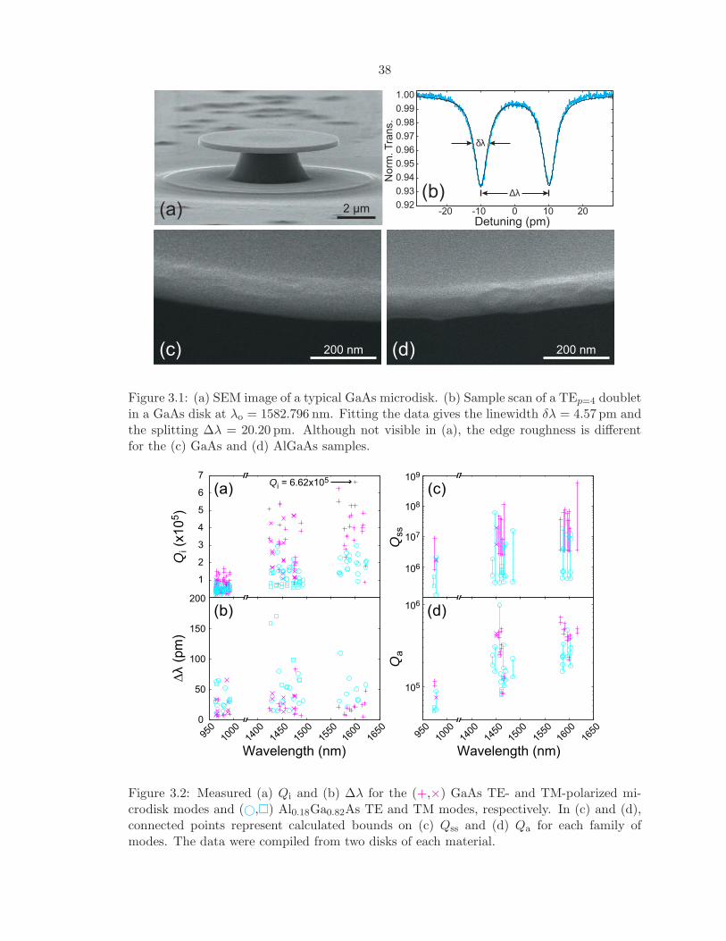
38
200 nm 200 nm
2 μmDetuning (pm)
No
rm. T
rans.
0-10-20 10 20
1.00
0.99
0.98
0.97
0.96
0.95
0.94
0.93
0.92
∆λ
δλ
(a)(b)
(c) (d)
Figure 3.1: (a) SEM image of a typical GaAs microdisk. (b) Sample scan of a TEp=4 doubletin a GaAs disk at λo = 1582.796 nm. Fitting the data gives the linewidth δλ = 4.57 pm andthe splitting ∆λ = 20.20 pm. Although not visible in (a), the edge roughness is differentfor the (c) GaAs and (d) AlGaAs samples.
1
2
3
4
5
6
7
Qi (
x10
5)
950
1000
1400
1450
1500
1550
1600
1650
0
50
100
150
Wavelength (nm)
∆λ (
pm
)
200
950
1000
1400
1450
1500
1550
1600
1650
Wavelength (nm)
105
106
106
107
108
109
Qa
Qss
Qi = 6.62x10⁵
(a)
(b)
(c)
(d)
Figure 3.2: Measured (a) Qi and (b) ∆λ for the (+,×) GaAs TE- and TM-polarized mi-crodisk modes and (©,) Al0.18Ga0.82As TE and TM modes, respectively. In (c) and (d),connected points represent calculated bounds on (c) Qss and (d) Qa for each family ofmodes. The data were compiled from two disks of each material.
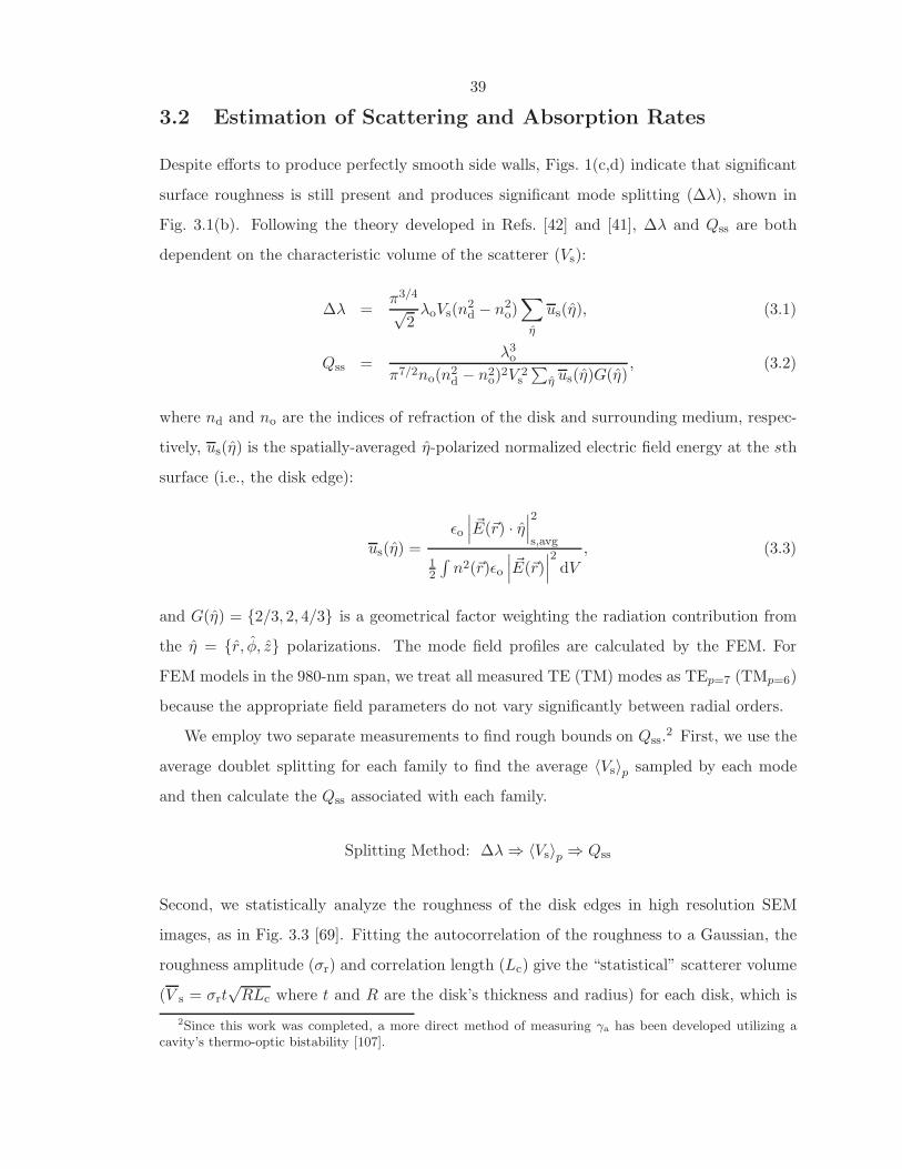
39
3.2 Estimation of Scattering and Absorption Rates
Despite efforts to produce perfectly smooth side walls, Figs. 1(c,d) indicate that significant
surface roughness is still present and produces significant mode splitting (∆λ), shown in
Fig. 3.1(b). Following the theory developed in Refs. [42] and [41], ∆λ and Qss are both
dependent on the characteristic volume of the scatterer (Vs):
∆λ =π3/4
√2λoVs(n
2d − n2
o)∑
η
us(η), (3.1)
Qss =λ3
o
π7/2no(n2d − n2
o)2V 2
s
∑
η us(η)G(η), (3.2)
where nd and no are the indices of refraction of the disk and surrounding medium, respec-
tively, us(η) is the spatially-averaged η-polarized normalized electric field energy at the sth
surface (i.e., the disk edge):
us(η) =ǫo
∣
∣
∣
~E(~r) · η∣
∣
∣
2
s,avg
12
∫
n2(~r)ǫo
∣
∣
∣
~E(~r)∣
∣
∣
2dV
, (3.3)
and G(η) = 2/3, 2, 4/3 is a geometrical factor weighting the radiation contribution from
the η = r, φ, z polarizations. The mode field profiles are calculated by the FEM. For
FEM models in the 980-nm span, we treat all measured TE (TM) modes as TEp=7 (TMp=6)
because the appropriate field parameters do not vary significantly between radial orders.
We employ two separate measurements to find rough bounds on Qss.2 First, we use the
average doublet splitting for each family to find the average 〈Vs〉p sampled by each mode
and then calculate the Qss associated with each family.
Splitting Method: ∆λ ⇒ 〈Vs〉p ⇒ Qss
Second, we statistically analyze the roughness of the disk edges in high resolution SEM
images, as in Fig. 3.3 [69]. Fitting the autocorrelation of the roughness to a Gaussian, the
roughness amplitude (σr) and correlation length (Lc) give the “statistical” scatterer volume
(V s = σrt√RLc where t and R are the disk’s thickness and radius) for each disk, which is
2Since this work was completed, a more direct method of measuring γa has been developed utilizing acavity’s thermo-optic bistability [107].
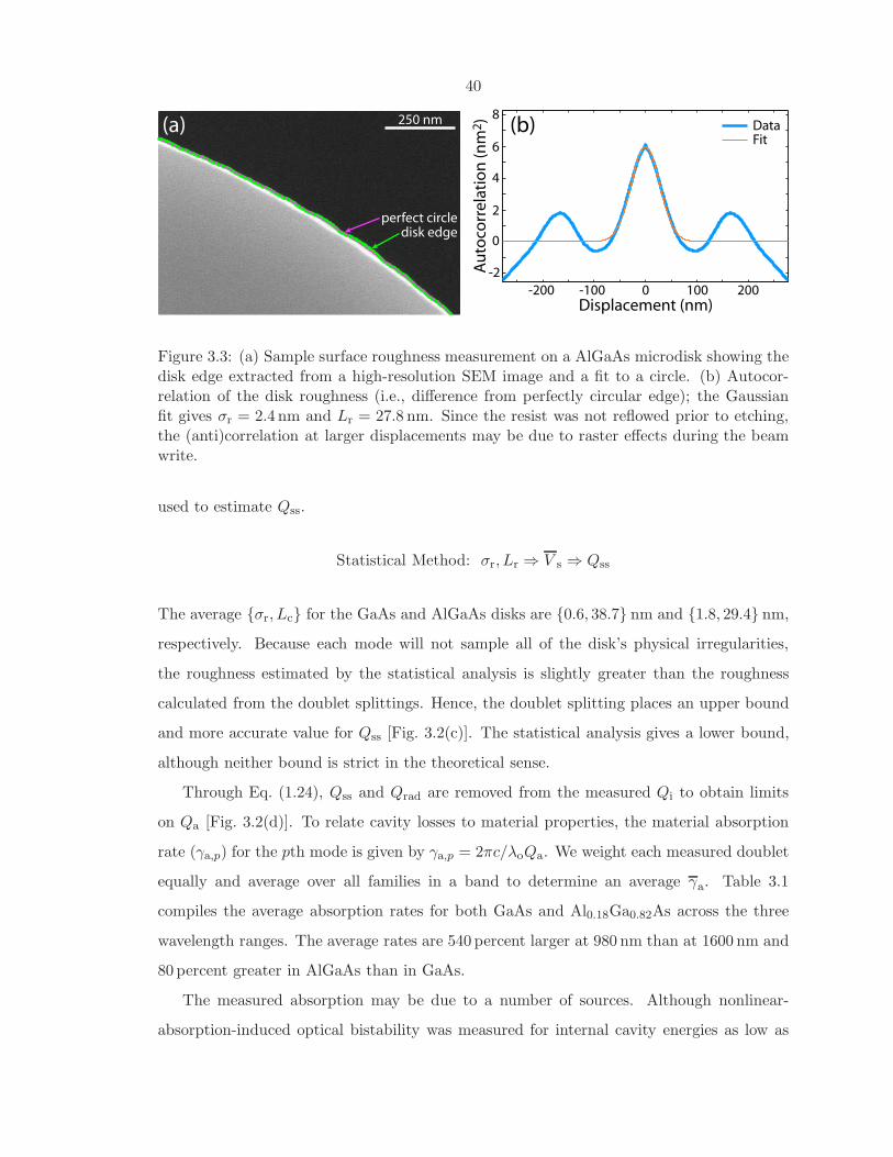
40
250 nm
disk edgeperfect circle
Displacement (nm)0-100-200 100 200
Au
toco
rre
lati
on
(n
m2)
-2
0
2
4
6
8DataFit
(a) (b)
Figure 3.3: (a) Sample surface roughness measurement on a AlGaAs microdisk showing thedisk edge extracted from a high-resolution SEM image and a fit to a circle. (b) Autocor-relation of the disk roughness (i.e., difference from perfectly circular edge); the Gaussianfit gives σr = 2.4 nm and Lr = 27.8 nm. Since the resist was not reflowed prior to etching,the (anti)correlation at larger displacements may be due to raster effects during the beamwrite.
used to estimate Qss.
Statistical Method: σr, Lr ⇒ V s ⇒ Qss
The average σr, Lc for the GaAs and AlGaAs disks are 0.6, 38.7 nm and 1.8, 29.4 nm,
respectively. Because each mode will not sample all of the disk’s physical irregularities,
the roughness estimated by the statistical analysis is slightly greater than the roughness
calculated from the doublet splittings. Hence, the doublet splitting places an upper bound
and more accurate value for Qss [Fig. 3.2(c)]. The statistical analysis gives a lower bound,
although neither bound is strict in the theoretical sense.
Through Eq. (1.24), Qss and Qrad are removed from the measured Qi to obtain limits
on Qa [Fig. 3.2(d)]. To relate cavity losses to material properties, the material absorption
rate (γa,p) for the pth mode is given by γa,p = 2πc/λoQa. We weight each measured doublet
equally and average over all families in a band to determine an average γa. Table 3.1
compiles the average absorption rates for both GaAs and Al0.18Ga0.82As across the three
wavelength ranges. The average rates are 540 percent larger at 980 nm than at 1600 nm and
80 percent greater in AlGaAs than in GaAs.
The measured absorption may be due to a number of sources. Although nonlinear-
absorption-induced optical bistability was measured for internal cavity energies as low as
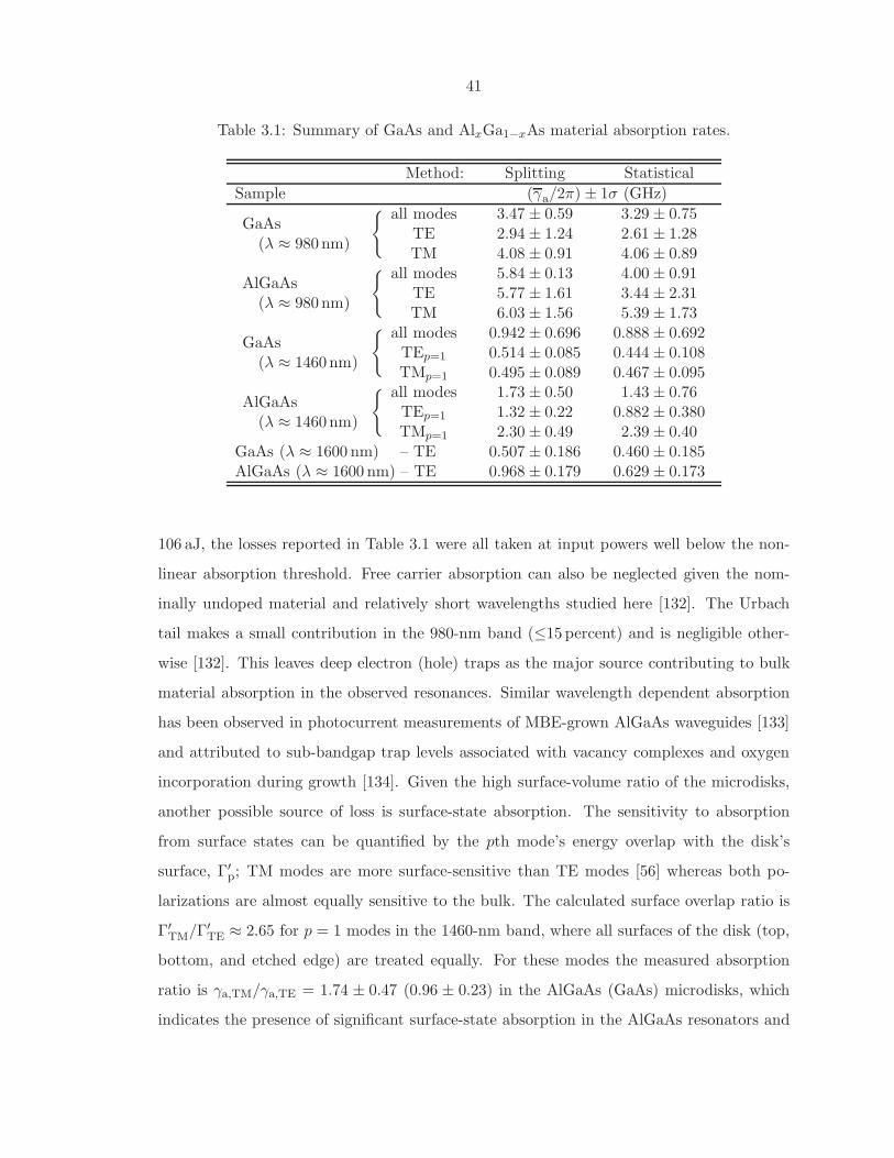
41
Table 3.1: Summary of GaAs and AlxGa1−xAs material absorption rates.
Method: Splitting Statistical
Sample (γa/2π) ± 1σ (GHz)
GaAs(λ ≈ 980 nm)
all modesTETM
3.47 ± 0.592.94 ± 1.244.08 ± 0.91
3.29 ± 0.752.61 ± 1.284.06 ± 0.89
AlGaAs(λ ≈ 980 nm)
all modesTETM
5.84 ± 0.135.77 ± 1.616.03 ± 1.56
4.00 ± 0.913.44 ± 2.315.39 ± 1.73
GaAs(λ ≈ 1460 nm)
all modesTEp=1
TMp=1
0.942 ± 0.6960.514 ± 0.0850.495 ± 0.089
0.888 ± 0.6920.444 ± 0.1080.467 ± 0.095
AlGaAs(λ ≈ 1460 nm)
all modesTEp=1
TMp=1
1.73 ± 0.501.32 ± 0.222.30 ± 0.49
1.43 ± 0.760.882 ± 0.3802.39 ± 0.40
GaAs (λ ≈ 1600 nm) – TE 0.507 ± 0.186 0.460 ± 0.185AlGaAs (λ ≈ 1600 nm) – TE 0.968 ± 0.179 0.629 ± 0.173
106 aJ, the losses reported in Table 3.1 were all taken at input powers well below the non-
linear absorption threshold. Free carrier absorption can also be neglected given the nom-
inally undoped material and relatively short wavelengths studied here [132]. The Urbach
tail makes a small contribution in the 980-nm band (≤15 percent) and is negligible other-
wise [132]. This leaves deep electron (hole) traps as the major source contributing to bulk
material absorption in the observed resonances. Similar wavelength dependent absorption
has been observed in photocurrent measurements of MBE-grown AlGaAs waveguides [133]
and attributed to sub-bandgap trap levels associated with vacancy complexes and oxygen
incorporation during growth [134]. Given the high surface-volume ratio of the microdisks,
another possible source of loss is surface-state absorption. The sensitivity to absorption
from surface states can be quantified by the pth mode’s energy overlap with the disk’s
surface, Γ′p; TM modes are more surface-sensitive than TE modes [56] whereas both po-
larizations are almost equally sensitive to the bulk. The calculated surface overlap ratio is
Γ′TM/Γ
′TE ≈ 2.65 for p = 1 modes in the 1460-nm band, where all surfaces of the disk (top,
bottom, and etched edge) are treated equally. For these modes the measured absorption
ratio is γa,TM/γa,TE = 1.74 ± 0.47 (0.96 ± 0.23) in the AlGaAs (GaAs) microdisks, which
indicates the presence of significant surface-state absorption in the AlGaAs resonators and
42
dominant bulk absorption in the GaAs disks. In the 980-nm band, the data is consistent
with bulk absorption [γa,TM/γa,TE = 1.05±0.40 (1.39±0.66) for the AlGaAs (GaAs) devices]
although the results are less conclusive due to the larger scatter in the data.
In summary, after accounting for radiation and surface scattering losses, we measure
greater sub-bandgap absorption in Al0.18Ga0.82As microdisks than in similar GaAs res-
onators, and the absorption in both materials decreases toward longer wavelengths. This
finding is at least partially reflected in recent cQED experiments with a single QD near or
in the strong-coupling regime [121–123, 135–142] that show the longest cavity photon life-
times (τph ≈ 70 ps) are achieved in devices at longer wavelengths (λo = 1294.5 nm) [138].3
From the polarization dependence of the measured optical loss, we infer that both surface
states and bulk states contribute to the residual absorption in these structures. Our results
imply that reductions in the optical loss of AlGaAs-based microphotonics, especially at the
shorter wavelengths of <1µm and in high Al content alloys, will require further study and
reduction of deep level traps, and that surface passivation techniques [143, 144] will also
likely be important.
3Longer cavity lifetimes (τph ≈ 80 ps at λo = 940.5 nm) have been demonstrated in large AlAs/GaAsmicropillars (d ≈ 5µm) with thick DBR mirrors (>32 layer pairs on each side of the defect) and loweccentricity, but Rabi splitting has only been observed in smaller pillars with higher loss (d = 3 µm withτph = 20ps) [139].
43
Chapter 4
Optical Processes in
Epitaxial c-Er2O3 on Silicon
Significant progress in the last decade has been made developing passive and active silicon
optical components; however, efficient generation of light within a Si platform remains a
technical and commercial challenge [79]. Efforts to incorporate Er3+ into the Si material
system, with erbium’s emission in the 1550-nm telecommunications band, have met with
limited success. Amorphous Er3+-doped glass waveguides on Si provide insufficient gain
(<4 dB/cm [145, 146]) for dense photonic integration, while doped silicon allotropes are
limited by other effects such as Auger recombination [147] and free-carrier absorption [148].
Here we describe the characterization of stoichiometric single-crystal Er2O3 grown on Si
by atomic layer epitaxy (ALE).1 We measure a peak resonant absorption of 364 dB/cm
at 1535 nm, negligible background absorption (<3 dB/cm), and strong cavity-polariton ef-
fects. The observed radiative efficiency from 1520 to 1650 nm is 0.09% with cooperative
upconversion producing strong green and red emission for Er3+ excitation levels as low as
2%.
Spurred by the growing power consumption of high-speed electrical interconnects for
multicore processors [149,150], optical networks have become an attractive option to achieve
Tb/s on-chip bandwidth [120,151,152]. Following the initial demonstration of silicon waveg-
uide devices [153], there has been significant development in adding optical functionality
to silicon microelectronics and, similarly, applying the efficiency and infrastructure of mod-
ern complementary metal-oxide-semiconductor (CMOS) processing to optical telecommu-
nication components. While silicon exhibits low loss across the 1300-nm and 1550-nm
1This work was done in collaboration with Translucent, Inc., where these epitaxial rare-earth oxide filmswere developed and characterized (XRD, RHEED, TEM, etc.).
44
telecommunication windows, unstrained silicon lacks any significant Pockels coefficient and
produces little emission from its 1.1 eV indirect bandgap [79]. Free-carrier dispersion and
four-wave mixing provide some inherent active functionality, such as modulation with rates
exceeding 1 GHz [154] and wavelength conversion [114], but considerable research, especially
concerning light emission and detection, has focused on integrating silicon with other optical
materials such as SiGe [155, 156] and the III-Vs [157, 158]. In this chapter we describe the
growth, processing, and optical properties of c-Er2O3 films on Si. Similar to stoichiomet-
ric polycrystalline Er3+ materials [159–164], Er2O3 allows for a 100-fold increase in Er3+
concentration over conventional Er-doped glasses [165], making it an attractive material for
on-chip emission and amplification in the 1550-nm wavelength band. Developed simulta-
neously for optoelectronic [166] and high-κ dielectric [167] applications, epitaxially grown
Er2O3 films can be incorporated into precisely controlled heterostructures and superlattices,
which may also allow for efficient electrical injection. Oxides incorporating multiple cation
species provide additional flexibility in designing the emission spectrum and dynamics as
a number of rare-earth ions may be interchangeable in the R2O3 lattice [168]. Beyond ap-
plication to chip-based optical networks, the strong cooperative upconversion within these
films may also be used for visible light generation in solid-state lighting and displays and
infrared-to-visible energy conversion in photovolatics.
4.1 Rare-Earth Ions in the R2O3 Bixbyite Lattice
The electronic configuration for elements in the lanthanide series is [Kr]4d104fx5s25p66s2
with additional electrons filling the 4f shell. Since the valence shell is constant, these atoms
are chemically similar and approximately the same size. Crystalline R2X3 compounds con-
taining trivalent rare-earth ions (e− configuration: [Kr]4d104fx−15s25p6) typically assume
two crystal structures: the hexagonal La2O3 structure and the cubic (Fe,Mn)2O3 bixbyite
structure. The hexagonal arrangement is more common among rare-earth oxysulfides and
oxyselenides while the bixbyite crystal is prevalent in sesquioxides when 0.60 . r(R)/r(O) .
0.87, where r is the ionic radius. Bixbyite’s large 16-molecule unit cell in Fig. 4.1(a) contains
32 metal ions with 24 distributed on low-symmerty sites (C2) and 8 on sites with inversion
symmetry (C3i). The bixbyite cell also contains 48 oxygen atoms arranged in an incomplete
cubic close packing [169].
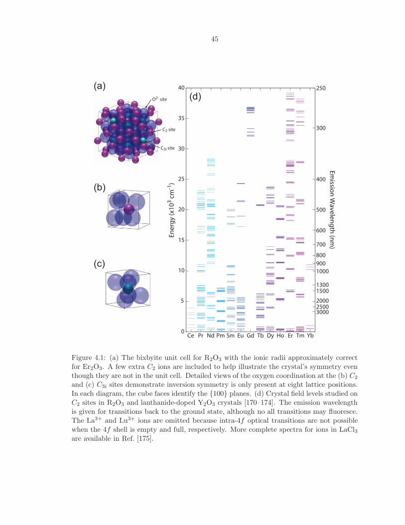
45
C2 site
O2- site
C3i site
Ce Pr Nd Pm Sm Eu Gd Tb Dy Ho Er Tm Yb0
5
10
15
20
25
30
35
40
En
erg
y (x
10
3 c
m-1
)
250
300
400
500
600
700
800
900
1000
13001500
200025003000
Em
ission
Wa
ve
len
gth
(nm
)
(a)
(b)
(c)
(d)
Figure 4.1: (a) The bixbyite unit cell for R2O3 with the ionic radii approximately correctfor Er2O3. A few extra C2 ions are included to help illustrate the crystal’s symmetry eventhough they are not in the unit cell. Detailed views of the oxygen coordination at the (b) C2
and (c) C3i sites demonstrate inversion symmetry is only present at eight lattice positions.In each diagram, the cube faces identify the 100 planes. (d) Crystal field levels studied onC2 sites in R2O3 and lanthanide-doped Y2O3 crystals [170–174]. The emission wavelengthis given for transitions back to the ground state, although no all transitions may fluoresce.The La3+ and Lu3+ ions are omitted because intra-4f optical transitions are not possiblewhen the 4f shell is empty and full, respectively. More complete spectra for ions in LaCl3are available in Ref. [175].
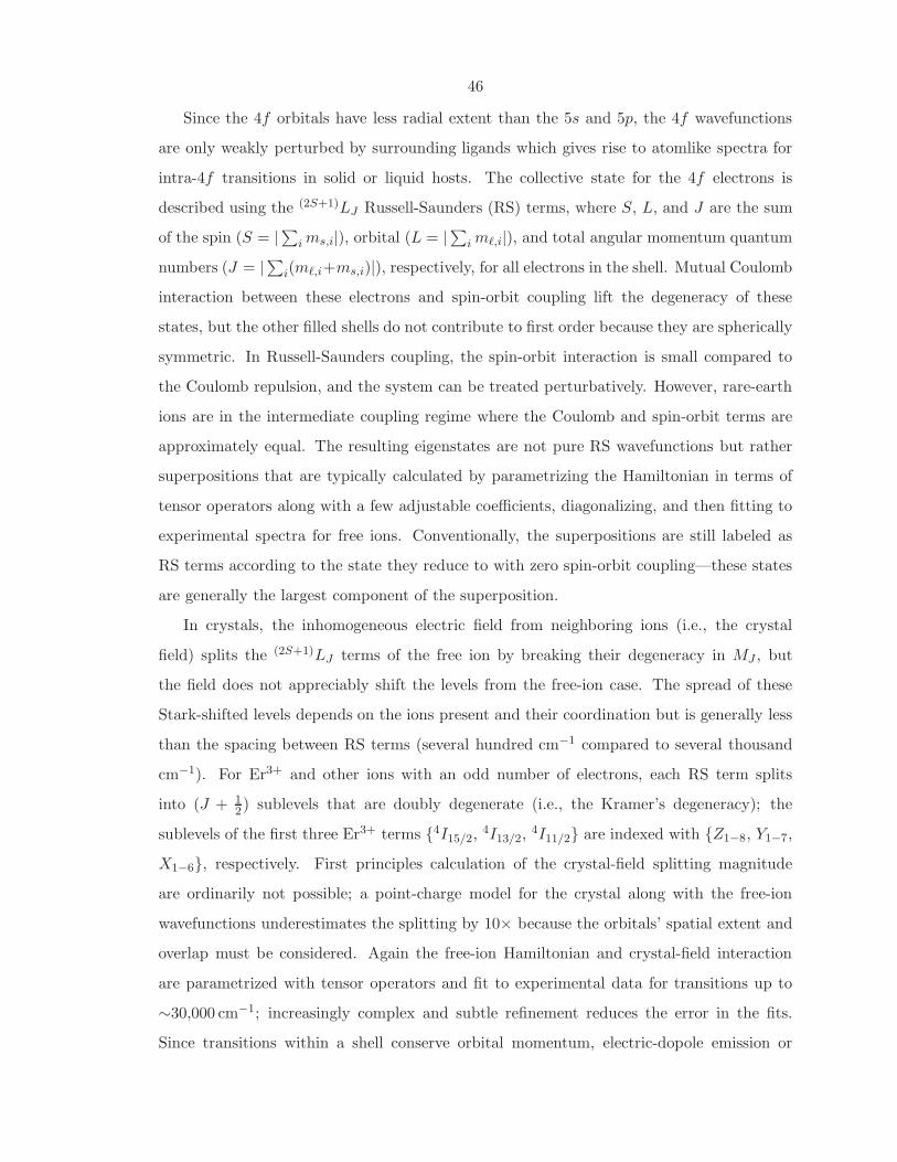
46
Since the 4f orbitals have less radial extent than the 5s and 5p, the 4f wavefunctions
are only weakly perturbed by surrounding ligands which gives rise to atomlike spectra for
intra-4f transitions in solid or liquid hosts. The collective state for the 4f electrons is
described using the (2S+1)LJ Russell-Saunders (RS) terms, where S, L, and J are the sum
of the spin (S = |∑ims,i|), orbital (L = |∑imℓ,i|), and total angular momentum quantum
numbers (J = |∑i(mℓ,i+ms,i)|), respectively, for all electrons in the shell. Mutual Coulomb
interaction between these electrons and spin-orbit coupling lift the degeneracy of these
states, but the other filled shells do not contribute to first order because they are spherically
symmetric. In Russell-Saunders coupling, the spin-orbit interaction is small compared to
the Coulomb repulsion, and the system can be treated perturbatively. However, rare-earth
ions are in the intermediate coupling regime where the Coulomb and spin-orbit terms are
approximately equal. The resulting eigenstates are not pure RS wavefunctions but rather
superpositions that are typically calculated by parametrizing the Hamiltonian in terms of
tensor operators along with a few adjustable coefficients, diagonalizing, and then fitting to
experimental spectra for free ions. Conventionally, the superpositions are still labeled as
RS terms according to the state they reduce to with zero spin-orbit coupling—these states
are generally the largest component of the superposition.
In crystals, the inhomogeneous electric field from neighboring ions (i.e., the crystal
field) splits the (2S+1)LJ terms of the free ion by breaking their degeneracy in MJ , but
the field does not appreciably shift the levels from the free-ion case. The spread of these
Stark-shifted levels depends on the ions present and their coordination but is generally less
than the spacing between RS terms (several hundred cm−1 compared to several thousand
cm−1). For Er3+ and other ions with an odd number of electrons, each RS term splits
into (J + 12) sublevels that are doubly degenerate (i.e., the Kramer’s degeneracy); the
sublevels of the first three Er3+ terms 4I15/2,4I13/2,
4I11/2 are indexed with Z1−8, Y1−7,
X1−6, respectively. First principles calculation of the crystal-field splitting magnitude
are ordinarily not possible; a point-charge model for the crystal along with the free-ion
wavefunctions underestimates the splitting by 10× because the orbitals’ spatial extent and
overlap must be considered. Again the free-ion Hamiltonian and crystal-field interaction
are parametrized with tensor operators and fit to experimental data for transitions up to
∼30,000 cm−1; increasingly complex and subtle refinement reduces the error in the fits.
Since transitions within a shell conserve orbital momentum, electric-dopole emission or
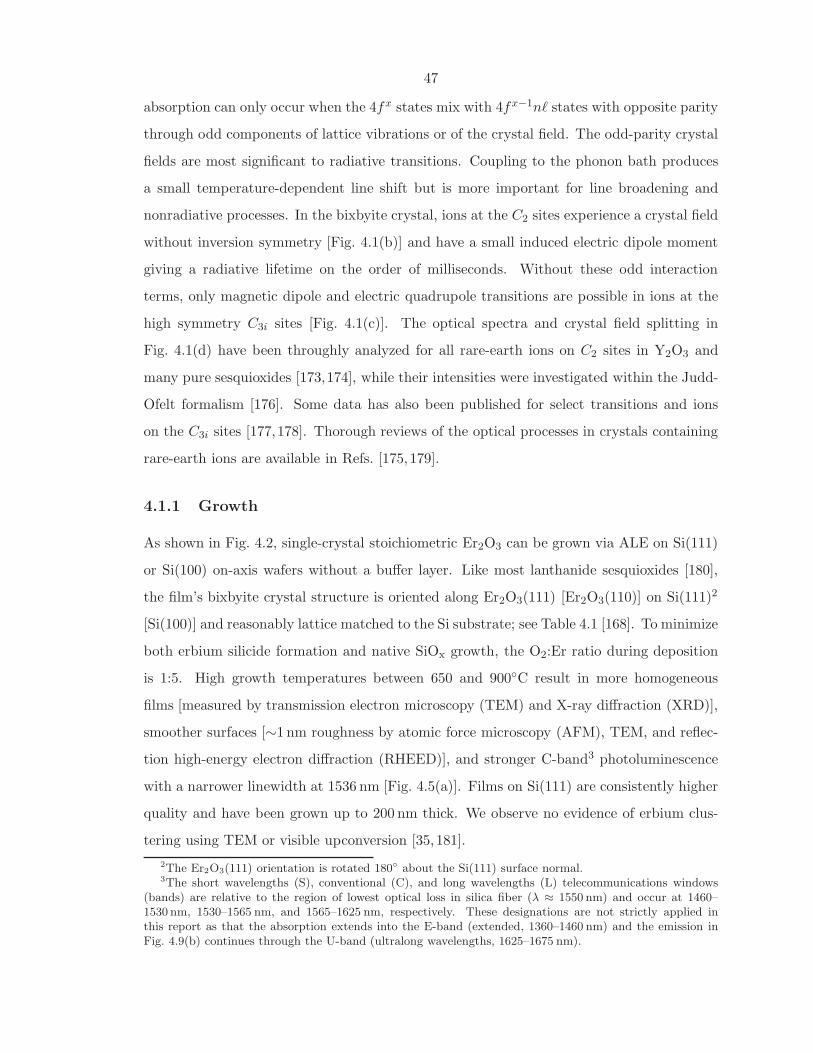
47
absorption can only occur when the 4fx states mix with 4fx−1nℓ states with opposite parity
through odd components of lattice vibrations or of the crystal field. The odd-parity crystal
fields are most significant to radiative transitions. Coupling to the phonon bath produces
a small temperature-dependent line shift but is more important for line broadening and
nonradiative processes. In the bixbyite crystal, ions at the C2 sites experience a crystal field
without inversion symmetry [Fig. 4.1(b)] and have a small induced electric dipole moment
giving a radiative lifetime on the order of milliseconds. Without these odd interaction
terms, only magnetic dipole and electric quadrupole transitions are possible in ions at the
high symmetry C3i sites [Fig. 4.1(c)]. The optical spectra and crystal field splitting in
Fig. 4.1(d) have been throughly analyzed for all rare-earth ions on C2 sites in Y2O3 and
many pure sesquioxides [173,174], while their intensities were investigated within the Judd-
Ofelt formalism [176]. Some data has also been published for select transitions and ions
on the C3i sites [177,178]. Thorough reviews of the optical processes in crystals containing
rare-earth ions are available in Refs. [175,179].
4.1.1 Growth
As shown in Fig. 4.2, single-crystal stoichiometric Er2O3 can be grown via ALE on Si(111)
or Si(100) on-axis wafers without a buffer layer. Like most lanthanide sesquioxides [180],
the film’s bixbyite crystal structure is oriented along Er2O3(111) [Er2O3(110)] on Si(111)2
[Si(100)] and reasonably lattice matched to the Si substrate; see Table 4.1 [168]. To minimize
both erbium silicide formation and native SiOx growth, the O2:Er ratio during deposition
is 1:5. High growth temperatures between 650 and 900C result in more homogeneous
films [measured by transmission electron microscopy (TEM) and X-ray diffraction (XRD)],
smoother surfaces [∼1 nm roughness by atomic force microscopy (AFM), TEM, and reflec-
tion high-energy electron diffraction (RHEED)], and stronger C-band3 photoluminescence
with a narrower linewidth at 1536 nm [Fig. 4.5(a)]. Films on Si(111) are consistently higher
quality and have been grown up to 200 nm thick. We observe no evidence of erbium clus-
tering using TEM or visible upconversion [35,181].
2The Er2O3(111) orientation is rotated 180 about the Si(111) surface normal.3The short wavelengths (S), conventional (C), and long wavelengths (L) telecommunications windows
(bands) are relative to the region of lowest optical loss in silica fiber (λ ≈ 1550 nm) and occur at 1460–1530 nm, 1530–1565 nm, and 1565–1625 nm, respectively. These designations are not strictly applied inthis report as that the absorption extends into the E-band (extended, 1360–1460 nm) and the emission inFig. 4.9(b) continues through the U-band (ultralong wavelengths, 1625–1675 nm).
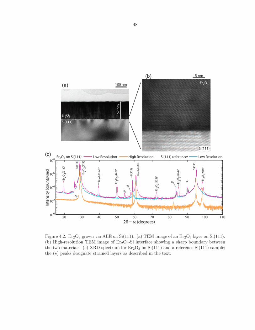
48
5 nm(b)
Er2O3
Si(111)
2θ − ω (degrees)
Inte
nsi
ty (
cou
nts
/se
c)
Er 2
O3
(42
2)*
KβW
W
Si(
11
1)
Si(
22
2) Si(
33
3)
Er 2
O3
(22
2)
Er 2
O3
(44
4)
Er 2
O3
(66
6)
Er 2
O3
(21
1)*
Er 2
O3
(44
2)*
Er 2
O3
(82
2)*
Er 2
O3
(84
4)*
20 30 40 50 60 70 80 90 100 110
102
104
106
108
(c)
Kβ
Kβ
100 nm(a)
Er2O3
Si(111)1
57
nm
100
Er2O3 on Si(111): Low Resolution High Resolution Si(111) reference: Low Resolution
Figure 4.2: Er2O3 grown via ALE on Si(111). (a) TEM image of an Er2O3 layer on Si(111).(b) High-resolution TEM image of Er2O3-Si interface showing a sharp boundary betweenthe two materials. (c) XRD spectrum for Er2O3 on Si(111) and a reference Si(111) sample;the (⋆) peaks designate strained layers as described in the text.
49
Table 4.1: Lattice constant (ao) and mismatch for R2O3 bixbyite crystals on (111)Si
Crystal ao (A) Mismatch⋆
Y2O3 10.604 –0.0238
La2O3 11.36 0.0458
Ce2O3† 11.16 0.0274
Pr2O3 11.152 0.0267
Nd2O3 11.077 0.0198
Pm2O3‡ 10.99 0.0118
Sm2O3 10.932 0.0064
Eu2O3 10.866 0.0004
Gd2O3 10.813 –0.0045
Tb2O3 10.730 –0.0122
Dy2O3 10.667 –0.0180
Ho2O3 10.607 –0.0235
Er2O3 10.547 –0.0290
Tm2O3 10.488 –0.0344
Yb2O3 10.439 –0.0389
Lu2O3 10.391 –0.0434
Si 5.431 —
⋆ The lattice mismatch is relative to twice the Si unit cell: (aROx/2aSi − 1).† Ce2O3 is readily oxidized to form CeO2 under ambient conditions.‡ Promethium is radioactive and has no isotopes with half-lives longer than 17.7 years.
In post-growth XRD analysis, the dominant peaks in Fig. 4.2(c) are due to the sub-
strate’s Si111 and film’s Er2O3111 planes. We employ two configurations for XRD
analysis using a standard Cu Kα source: (1) a low angular resolution configuration that
is sensitive to more material phases and (2) a high angular resolution configuration. The
low-resolution setup utilizes a mirror to provide a wider angular divergence and higher in-
tensity (shorter integration times) for the X-rays. With the 〈110〉 wafer flat of the Si(111)
substrate 30 misaligned from the X-ray beam, this measurement is sensitive to more sec-
ondary material phases as in Fig. 4.2(b). Lesser peaks are associated with additional lines
from the X-ray source (Kβ , W) and with diffraction from minority Er2O3 phases; there is
no XRD evidence of erbium silicates or silicides at the Er2O3-Si interface [167, 182, 183].
The 211, 442, and 822 families of peaks correspond to slightly strained volumes with
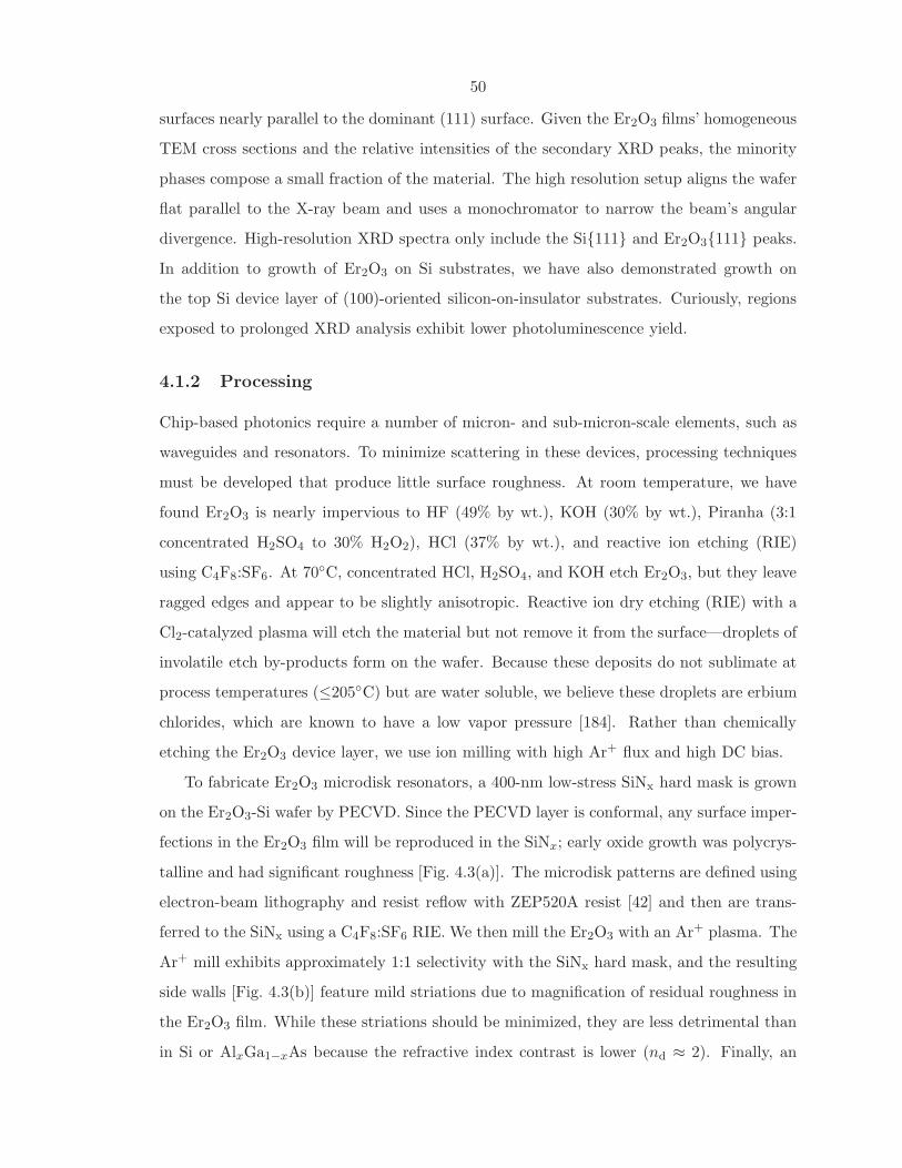
50
surfaces nearly parallel to the dominant (111) surface. Given the Er2O3 films’ homogeneous
TEM cross sections and the relative intensities of the secondary XRD peaks, the minority
phases compose a small fraction of the material. The high resolution setup aligns the wafer
flat parallel to the X-ray beam and uses a monochromator to narrow the beam’s angular
divergence. High-resolution XRD spectra only include the Si111 and Er2O3111 peaks.
In addition to growth of Er2O3 on Si substrates, we have also demonstrated growth on
the top Si device layer of (100)-oriented silicon-on-insulator substrates. Curiously, regions
exposed to prolonged XRD analysis exhibit lower photoluminescence yield.
4.1.2 Processing
Chip-based photonics require a number of micron- and sub-micron-scale elements, such as
waveguides and resonators. To minimize scattering in these devices, processing techniques
must be developed that produce little surface roughness. At room temperature, we have
found Er2O3 is nearly impervious to HF (49% by wt.), KOH (30% by wt.), Piranha (3:1
concentrated H2SO4 to 30% H2O2), HCl (37% by wt.), and reactive ion etching (RIE)
using C4F8:SF6. At 70C, concentrated HCl, H2SO4, and KOH etch Er2O3, but they leave
ragged edges and appear to be slightly anisotropic. Reactive ion dry etching (RIE) with a
Cl2-catalyzed plasma will etch the material but not remove it from the surface—droplets of
involatile etch by-products form on the wafer. Because these deposits do not sublimate at
process temperatures (≤205C) but are water soluble, we believe these droplets are erbium
chlorides, which are known to have a low vapor pressure [184]. Rather than chemically
etching the Er2O3 device layer, we use ion milling with high Ar+ flux and high DC bias.
To fabricate Er2O3 microdisk resonators, a 400-nm low-stress SiNx hard mask is grown
on the Er2O3-Si wafer by PECVD. Since the PECVD layer is conformal, any surface imper-
fections in the Er2O3 film will be reproduced in the SiNx; early oxide growth was polycrys-
talline and had significant roughness [Fig. 4.3(a)]. The microdisk patterns are defined using
electron-beam lithography and resist reflow with ZEP520A resist [42] and then are trans-
ferred to the SiNx using a C4F8:SF6 RIE. We then mill the Er2O3 with an Ar+ plasma. The
Ar+ mill exhibits approximately 1:1 selectivity with the SiNx hard mask, and the resulting
side walls [Fig. 4.3(b)] feature mild striations due to magnification of residual roughness in
the Er2O3 film. While these striations should be minimized, they are less detrimental than
in Si or AlxGa1−xAs because the refractive index contrast is lower (nd ≈ 2). Finally, an
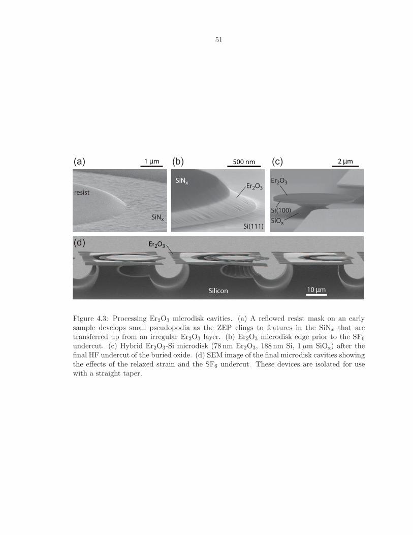
51
500 nm(b)
Si(111)
SiNxEr2O3
2 µm(c)
Si(100)
Er2O3
SiOxSiNx
resist
(a) 1 µm
10 µm
(d) Er2O3
Silicon
Figure 4.3: Processing Er2O3 microdisk cavities. (a) A reflowed resist mask on an earlysample develops small pseudopodia as the ZEP clings to features in the SiNx that aretransferred up from an irregular Er2O3 layer. (b) Er2O3 microdisk edge prior to the SF6
undercut. (c) Hybrid Er2O3-Si microdisk (78 nm Er2O3, 188 nm Si, 1µm SiOx) after thefinal HF undercut of the buried oxide. (d) SEM image of the final microdisk cavities showingthe effects of the relaxed strain and the SF6 undercut. These devices are isolated for usewith a straight taper.
52
isotropic SF6 dry etch simultaneously partially undercuts the silicon substrate and removes
the remaining SiNx mask. Once the film is released from the substrate in Fig. 4.3(d), the
cavities “flower” as the compressively strained film partially relaxes. Since residual organ-
ics cannot be removed from this material using Piranha, initial tests indicate a zero-bias
O2 plasma will clean the surface and not damage the epitaxy. Given its low reactivity,
the Er2O3 layer provides a convenient mask for subsequent processing of hybrid structures.
Processing hybrid Er2O3-Si resonators from Er2O3-SOI wafers, as in Fig. 4.3(c), employs
the same SiNx hard mask and Ar+ mill. With the Er2O3 layer acting as a mask, we etch
the silicon device layer with an anisotropic C4F8:SF6 RIE and undercut the buried oxide
with concentrated HF. Many samples are prepared to optimize the process parameters at
each step in order to minimize the microdisk side wall roughness. The measurements de-
scribed here concern ∼150 nm thick Er2O3 on Si(111) and Er2O3 microdisks with a radius
of ∼20µm.
4.2 Optical Properties
Once the SiNx is removed and the disks are undercut, the emission and absorption properties
of Er2O3 are again investigated using dimpled fiber-taper waveguides to characterize the
disks’ WGMs and excite the Er3+ optical transitions. The fiber-taper also offers high
photoluminescence collection efficiency from both the WGMs (∼10%) [70] and unpatterned
film (∼0.1%) [185]. Once fiber coupled, the pump and emission can be easily demultiplexed
for sensitive pump-probe and pulsed measurements. The cavity dimensions (R ≈ 20µm
and h = 150 nm) are chosen to give minimal bending loss across the S/C/L-bands and
well separated TE first- and second-order radial modes, as in Fig. 4.4. Conveniently, these
cavity modes and the taper waveguide are almost phase matched (ncaveff ≈ 1.17 and nwg
eff ≈1.26), which gives near critical coupling for a wide range (1450–1560 nm) when the taper
is placed in contact with the disk edge. For a fixed taper position, WGMs across the
S/C/L bands exhibit different coupling depths because of the Er3+ absorption spectrum.
On the edges of the absorption band (near 1420 and 1620 nm), γi ≪ γe, and the resonances
are significantly over coupled. In the center of the band, γi ≈ γe, and the modes are near
critical coupling. The shallower transmission features near 1535 and 1549 nm are attributed
to cavity-polariton and single-pass absorption effects.
53
1440 1460 1480 1500 1520 1540 1560 1580 1600 1620
No
rm. T
ran
s.
Wavelength (nm)
1.0
0.8
0.6
0.4
0.2
0.01420
Figure 4.4: Microdisk transmission spectrum for quasi-TE modes of a cavity with R ≈20µm; the fundamental radial-order WGMs are highlighted (gray).
4.2.1 Absorption and Emission Spectra for the 4I 13/2→4
I 15/2 Transition
To observe the crystal-field Stark splitting for the 4I13/2→4I15/2 transition in this crystalline
host, we measure both the room temperature photoluminescence (PL) and absorption spec-
tra. We obtain the emission spectrum by placing the fiber-taper in contact with an under-
cut part of the film and pumping at λ = 981.4 nm (exciting the X1 sublevel in the 4I11/2
term). The fiber-collected luminescence [Fig. 4.5(a)] displays little inhomogeneous broad-
ening of the Er3+ transitions compared to amorphous hosts, and is qualitatively similar to
the spectrum reported for polycrystalline Er2O3 deposited by pulsed-laser ablation [163].
In comparison to large crystals of Er2O3 and dilute Er3+-doped Y2O3 produced by flame
fusion [172,178], the low temperature PL spectrum of these Er2O3 films exhibit more inho-
mogeneous broadening, also shown in Fig. 4.5(a). The 8 K PL also indicates some of these
lines may be homogeneously broadened at room temperature—e.g., the linewidth for the
1549 nm peak is 56.6 GHz at 8 K and 134.7 GHz at 300 K.
The absorption spectrum [Fig. 4.5(b)] can be determined by fitting the low-power in-
trinsic loss rate of many TEp=1 WGMs. While this WGM-linewidth method gives a digital
rather than continuous spectrum, it involves measuring spectral widths rather than intensity
changes, and coupling losses are insignificant and easily calculated from cavity-waveguide
loading. Since there are several loss mechanisms that contribute to γi, radiation and sur-
face scattering losses must be accounted for when using cavity modes to determine the
absorption spectrum (similar to §3.2). By choosing appropriate cavity dimensions, the cal-
culated γrad is negligible for the fundamental modes: γrad < 82 MHz = 0.026 cm−1. Since
Rayleigh scattering increases toward longer wavelengths [41, 69], scattering losses can be
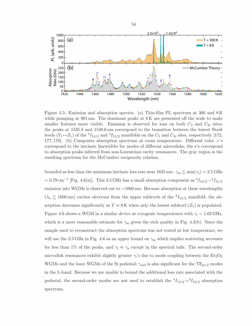
54
0
200
400
600
800
1000
PL
(a
rb. u
nit
s)
1420 1440 1460 1480 1500 1520 1540 1560 1580 1600 1620
50
100
150
200
250
A
bso
rpti
on
Ra
te (
GH
z)
Wavelength (nm)
0
T = 300 K
T = 8 K
(a)
(b)
2.3x10³ 1.3x10⁴
McCumber Theory
Figure 4.5: Emission and absorption spectra. (a) Thin-film PL spectrum at 300 and 8Kwhile pumping at 981 nm. The dominant peaks at 8K are presented off the scale to makesmaller features more visible. Emission is observed for ions on both C2 and C3i sites;the peaks at 1535.8 and 1548.6 nm correspond to the transition between the lowest Starklevels (Y1↔Z1) of the 4I13/2 and 4I15/2 manifolds on the C2 and C3i sites, respectively [172,177, 178]. (b) Composite absorption spectrum at room temperature. Different color ×’scorrespond to the intrinsic linewidths for modes of different microdisks; the ⋆’s correspondto absorption peaks inferred from non-Lorentzian cavity resonances. The gray region is theresulting spectrum for the McCumber reciprocity relation.
bounded as less than the minimum intrinsic loss rate near 1625 nm: γss . min(γi) = 2.5 GHz
= 0.79 cm−1 [Fig. 4.6(a)]. This 2.5 GHz has a small absorption component as 4I13/2→4I15/2
emission into WGMs is observed out to ∼1660 nm. Because absorption at these wavelengths
(λo & 1600 nm) excites electrons from the upper sublevels of the 4I15/2 manifold, the ab-
sorption decreases significantly at T ≈ 8 K when only the lowest sublevel (Z1) is populated.
Figure 4.6 shows a WGM in a similar device at cryogenic temperatures with γi = 1.02 GHz,
which is a more reasonable estimate for γss given the etch quality in Fig. 4.3(b). Since the
sample used to reconstruct the absorption spectrum was not tested at low temperature, we
will use the 2.5 GHz in Fig. 4.6 as an upper bound on γss which implies scattering accounts
for less than 1% of the peaks, and γi ≈ γa except in the spectral tails. The second-order
microdisk resonances exhibit slightly greater γi’s due to mode coupling between the Er2O3
WGMs and the lossy WGMs of the Si pedestal; γrad is also significant for the TEp=2 modes
in the L-band. Because we are unable to bound the additional loss rate associated with the
pedestal, the second-order modes are not used to establish the 4I15/2→4I13/2 absorption
spectrum.
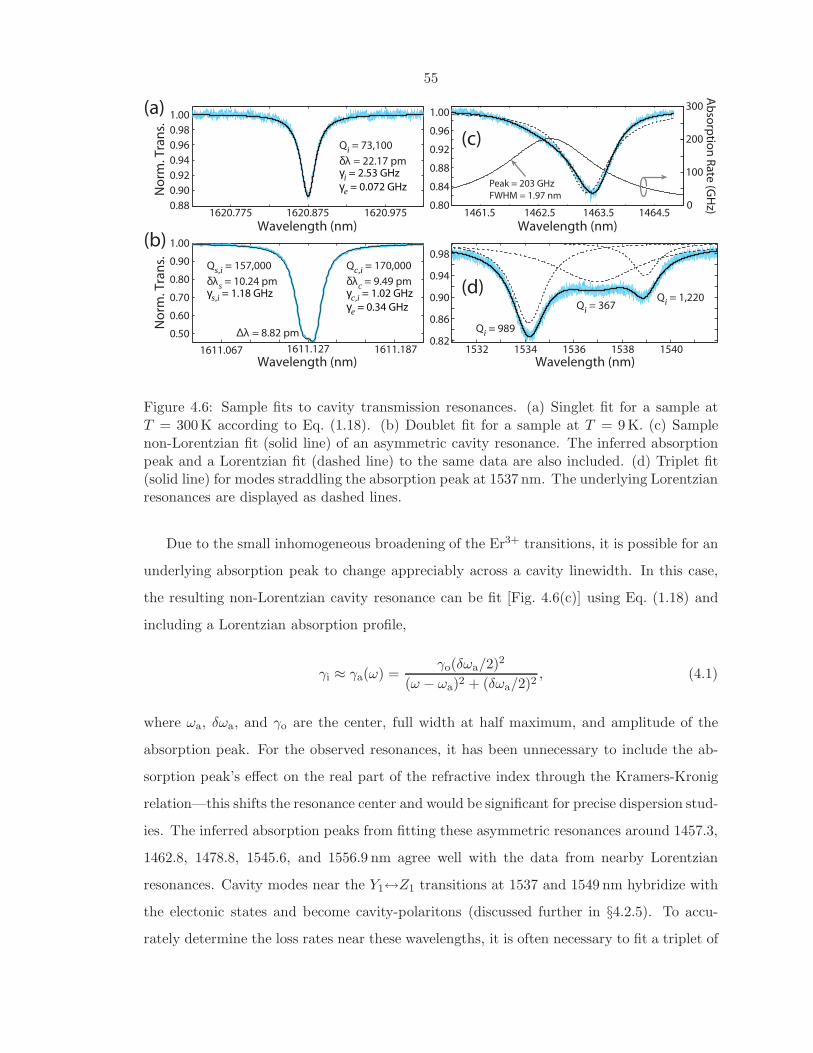
55
1620.775 1620.875 1620.9750.88
0.90
0.92
0.94
0.96
0.98
1.00
Wavelength (nm)
No
rm. T
ran
s.δλ = 22.17 pm
Qi = 73,100
γi = 2.53 GHz
γe = 0.072 GHz
1461.5 1462.5 1463.5 1464.50.80
0.84
0.88
0.92
0.96
1.00
Wavelength (nm)
0
100
200
300A
bso
rptio
n R
ate
(GH
z)
Peak = 203 GHz
FWHM = 1.97 nm
(a)
(c)N
orm
. Tra
ns.
0.50
0.60
0.70
0.80
0.90
1.00
1611.127 1611.1871611.067Wavelength (nm)
δλc = 9.49 pm
Qc,i = 170,000
γc,i = 1.02 GHz
γe = 0.34 GHz
δλs = 10.24 pm
Qs,i = 157,000
γs,i = 1.18 GHz
∆λ = 8.82 pm0.82
0.86
0.90
0.94
0.98
1532 1534 1536 1538 1540
Wavelength (nm)
Qi = 989
Qi = 367Qi = 1,220
(b)
(d)
Figure 4.6: Sample fits to cavity transmission resonances. (a) Singlet fit for a sample atT = 300 K according to Eq. (1.18). (b) Doublet fit for a sample at T = 9 K. (c) Samplenon-Lorentzian fit (solid line) of an asymmetric cavity resonance. The inferred absorptionpeak and a Lorentzian fit (dashed line) to the same data are also included. (d) Triplet fit(solid line) for modes straddling the absorption peak at 1537 nm. The underlying Lorentzianresonances are displayed as dashed lines.
Due to the small inhomogeneous broadening of the Er3+ transitions, it is possible for an
underlying absorption peak to change appreciably across a cavity linewidth. In this case,
the resulting non-Lorentzian cavity resonance can be fit [Fig. 4.6(c)] using Eq. (1.18) and
including a Lorentzian absorption profile,
γi ≈ γa(ω) =γo(δωa/2)
2
(ω − ωa)2 + (δωa/2)2, (4.1)
where ωa, δωa, and γo are the center, full width at half maximum, and amplitude of the
absorption peak. For the observed resonances, it has been unnecessary to include the ab-
sorption peak’s effect on the real part of the refractive index through the Kramers-Kronig
relation—this shifts the resonance center and would be significant for precise dispersion stud-
ies. The inferred absorption peaks from fitting these asymmetric resonances around 1457.3,
1462.8, 1478.8, 1545.6, and 1556.9 nm agree well with the data from nearby Lorentzian
resonances. Cavity modes near the Y1↔Z1 transitions at 1537 and 1549 nm hybridize with
the electonic states and become cavity-polaritons (discussed further in §4.2.5). To accu-
rately determine the loss rates near these wavelengths, it is often necessary to fit a triplet of
56
modes (two polariton modes and a neighboring broad WGM). This fit can be accomplished
by modifying Eq. (1.17a) to include two additional modes:
t(ωℓ) = s + i√γe,1acw,1(ωℓ, ω1) + i
√γe,2acw,2(ωℓ, ω2) + i
√γe,3acw,3(ωℓ, ω3). (4.2)
This approximation holds for weakly coupled WGMs as long as the phase shift of t is small.
When the modes are more deeply coupled, Eq. (4.2) does not accurately account for the
interference between the modes, and the resulting fits describe a system that does not
conserve energy. After extracting the three absorption rates from data like Fig. 4.6(d), the
rate for the p = 1 mode is identified and used in Fig. 4.5(b). When the TEp=1 mode is
resonant with the absorption peak, the cavity and electronic linewidths average, and the
linewidth for either polariton branch can be used.
The absorption spectrum can also be obtained using the McCumber reciprocity relation
between the absorption (σa) and emission (σe) cross sections [165]. Since the crystal field
splitting of a RS term is approximately equal to or greater than the thermal energy, the
occupation probabilities for the sublevels are not equal, and the relationship between the
total absorption and emission rates between two levels (arising from the Einstein A and
B coefficients) no longer holds. Within a single manifold, the electrons will thermalize
on a time scale of ∼100 ps via interactions with the phonon bath. On the millisecond
timescale for radiative transitions, the thermal distribution within the sublevels biases the
emission (absorption) toward red (blue) wavelengths. This situation is identical to phonon-
terminated lasers [186], and the cross sections are related by
σa(ω) =
(
Z2
Z1
)
σe(ω) exp
(
ℏω − E21
kBT
)
, (4.3)
where E21 is the energy difference between the two manifolds, Z2 and Z1 are the partition
functions for sublevels within the upper and lower manifolds, kB is the Boltzmann constant,
and T is the temperature. Unlike in glass, spectroscopy of the Stark levels is available for
ions in many crystals [e.g., Fig. 4.1(d)], and Eq. (4.3) can be evaluated exactly. Using
the energies for the sublevels of 4I13/2 and 4I15/2 on C2 from Ref. [172], the results from
Eq. (4.3) in Fig. 4.5(b) are in reasonable agreement with the linewidth data. The McCumber
spectrum is scaled to the maximum absorption peak at 1535 nm because the magnitude
57
of the PL data is not calibrated. The shortcoming of this approach is that it assumes
the dipoles are identical and independent. These assumptions are valid in many systems
such as lightly doped glasses, but neither are strictly true in Er2O3. Differences between
the McCumber theory and the data occur primarily at the edges of the spectrum and
may reflect different dynamics for ions on the C2 and C3i sites. As will be discussed in
the following sections, emission from the magnetic dipole transitions on the C3i sites is
disproportionately large for the observed absorption, and the excitation migration rate
(§4.2.3) may be asymmetric for transfers between the C2 and C3i sublattices.
The resulting spectrum [Fig. 4.5(b)] again reflects the weak inhomogeneous broadening
of the Er3+ transitions and qualitatively agrees with the peaks’ positions and widths in the
PL spectrum. Accounting for material and modal dispersion with scattering losses bound
at <1% of the peak values, the absorption maxima of 267.0 GHz at 1535 nm and 175.4 GHz
at 1479 nm correspond to 83.9 cm−1 (δωfsr/2π ≈ 1.59 THz) and 56.2 cm−1 (δωfsr/2π ≈1.56 THz), respectively. The narrow peaks and low losses in the tails further indicate there
is little background absorption, and all 83.9 cm−1 (364 dB/cm) can be attributed to resonant
4I15/2→4I13/2 excitation, which sets a high maximum value for potential gain.
4.2.2 Upconversion
While the 1450–1650 nm band is most useful for hybrid Er3+-silicon optical networks, up-
conversion into visible transitions is also present and has been partly investigated for poly-
crystalline Er2O3 on Si [159,162]. We determine the upconversion spectrum by transferring
a small piece (∼2µm2 × 150 nm) of Er2O3 onto the fiber-taper and pumping with <3 mW
at 1536.7 nm. The taper-collected PL is then measured in a Czerny-Turner spectrometer
with a silicon CCD camera. The visible PL contains emission from many levels with sig-
nificant emission near 550 and 670 nm and exhibits little inhomogeneous broadening, as in
Fig. 4.5(a). The relative intensities in Fig.4.7(a,b) may not reflect the actual strength of
each transition because we are unable to correct for the unknown taper collection efficiency
across the visible range; we have corrected for the grating and CCD efficiencies. Spectro-
scopic data over a large range must also be corrected for second-order diffraction from the
spectrometer—i.e., the grating equation for a given diffraction angle (θd) is simultaneously
satisfied for wavelengths (λj) in two different orders (mj): a(sin θd− sin θi) = m1λ1 = m2λ2
where a is the grating pitch and θi is the incident angle. Usually gratings are blazed to
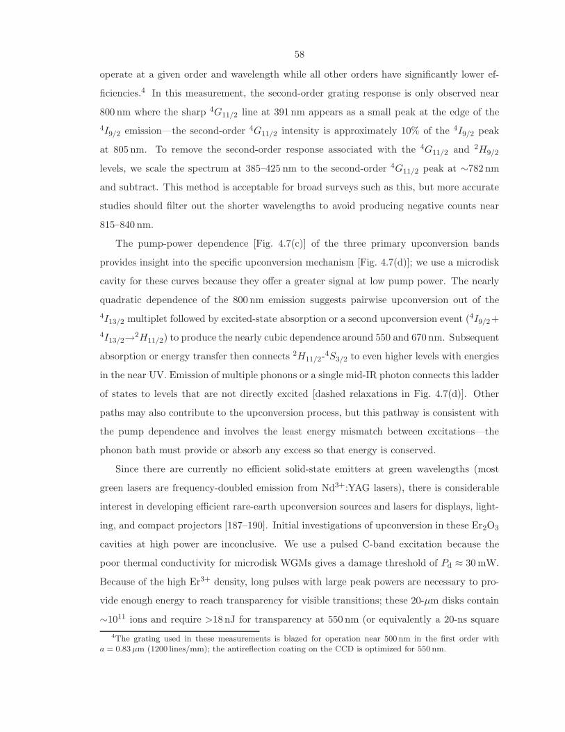
58
operate at a given order and wavelength while all other orders have significantly lower ef-
ficiencies.4 In this measurement, the second-order grating response is only observed near
800 nm where the sharp 4G11/2 line at 391 nm appears as a small peak at the edge of the
4I9/2 emission—the second-order 4G11/2 intensity is approximately 10% of the 4I9/2 peak
at 805 nm. To remove the second-order response associated with the 4G11/2 and 2H9/2
levels, we scale the spectrum at 385–425 nm to the second-order 4G11/2 peak at ∼782 nm
and subtract. This method is acceptable for broad surveys such as this, but more accurate
studies should filter out the shorter wavelengths to avoid producing negative counts near
815–840 nm.
The pump-power dependence [Fig. 4.7(c)] of the three primary upconversion bands
provides insight into the specific upconversion mechanism [Fig. 4.7(d)]; we use a microdisk
cavity for these curves because they offer a greater signal at low pump power. The nearly
quadratic dependence of the 800 nm emission suggests pairwise upconversion out of the
4I13/2 multiplet followed by excited-state absorption or a second upconversion event (4I9/2+
4I13/2→2H11/2) to produce the nearly cubic dependence around 550 and 670 nm. Subsequent
absorption or energy transfer then connects 2H11/2-4S3/2 to even higher levels with energies
in the near UV. Emission of multiple phonons or a single mid-IR photon connects this ladder
of states to levels that are not directly excited [dashed relaxations in Fig. 4.7(d)]. Other
paths may also contribute to the upconversion process, but this pathway is consistent with
the pump dependence and involves the least energy mismatch between excitations—the
phonon bath must provide or absorb any excess so that energy is conserved.
Since there are currently no efficient solid-state emitters at green wavelengths (most
green lasers are frequency-doubled emission from Nd3+:YAG lasers), there is considerable
interest in developing efficient rare-earth upconversion sources and lasers for displays, light-
ing, and compact projectors [187–190]. Initial investigations of upconversion in these Er2O3
cavities at high power are inconclusive. We use a pulsed C-band excitation because the
poor thermal conductivity for microdisk WGMs gives a damage threshold of Pd ≈ 30 mW.
Because of the high Er3+ density, long pulses with large peak powers are necessary to pro-
vide enough energy to reach transparency for visible transitions; these 20-µm disks contain
∼1011 ions and require >18 nJ for transparency at 550 nm (or equivalently a 20-ns square
4The grating used in these measurements is blazed for operation near 500 nm in the first order witha = 0.83 µm (1200 lines/mm); the antireflection coating on the CCD is optimized for 550 nm.
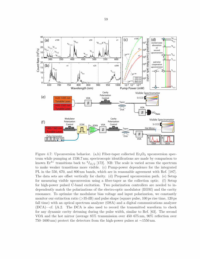
59
300 350 400 450 500 550 6000
10
20
30
650 700 750 800 850 900 950 10000
5
10
15
Wavelength (nm)
Co
un
t R
ate
(1
03
/s)
10-2
Pump Power (mW)
Inte
gra
ted
Co
un
t Ra
te (a
rb. u
nits)
550 nm670 nm800 nm
(c) (d)
pairwise
cooperative
upconversion
excited state
absorption
or
second
upconversion
4I15/2
4I13/2
4I11/2
4I9/2
4F9/2
2H11/2
4S3/2
(a)
4I11/24I
9/2
4F9/2
(b) x1 x25 x200
40
20
2H11/2
& 4S3/2
4F7/2
4F5/2
2H9/2
4G11/2
2K13/2
x100 x50 x1
2G5/2
2P1/2
4G7/22D
5/2
∝P2.62
∝P2.74
∝P1.84
x1
x1
x100
(e) 1420-1495 nm
Tunable Laser
1495-1565 nm
Tunable Laser Disk
Taper
PDTrans
VOA
Visible Spectrometer
Si CCDVOA
1495-1565 nm
Tunable Laser
VOA
Modulator
Polarization
Control
Disk
Taper
OSA
EDFA
Pulse GeneratorSYNC OUT
DCA
Cavity
Polarization
Control
Visible Spectrometer
Si CCD
VOA
EOM
Hot Mirror
(f )
Cavity
Polarization
Control
10-1 10-0
102
103
104
105
106
107
Figure 4.7: Upconversion behavior. (a,b) Fiber-taper collected Er2O3 upconversion spec-trum while pumping at 1536.7 nm; spectroscopic identifications are made by comparison toknown Er3+ transitions back to 4I15/2 [172]. NB: The scale is varied across the spectrumto make weaker transitions more visible. (c) Pump-power dependence for the integratedPL in the 550, 670, and 800 nm bands, which are in reasonable agreement with Ref. [187].The data sets are offset vertically for clarity. (d) Proposed upconversion path. (e) Setupfor measuring visible upconversion using a fiber-taper as the collection optic. (f) Setupfor high-power pulsed C-band excitation. Two polarization controllers are needed to in-dependently match the polarizations of the electro-optic modulator (EOM) and the cavityresonance. To optimize the modulator bias voltage and input polarization, we constantlymonitor our extinction ratio (>35 dB) and pulse shape (square pulse, 100 ps rise time, 120 psfall time) with an optical spectrum analyzer (OSA) and a digital communications analyzer(DCA)—cf. §A.2. The DCA is also used to record the transmitted waveform to checkfor any dynamic cavity detuning during the pulse width, similar to Ref. [63]. The secondVOA and the hot mirror (average 85% transmission over 450–675 nm, 90% reflection over750–1600 nm) protect the detectors from the high-power pulses at ∼1550 nm.

60
pulse with a peak power of 900 mW). To generate these long high-energy pulses in the C-
band, we modulate the input to an erbium-doped fiber amplifier (EDFA). Pulses with a
high-extinction ratio and low duty cycle can fully extract the energy stored in the amplifier
and produce peak powers well above the saturation output, which is usually specified for CW
operation. With 10 mW from the tunable diode laser, the arrangment in Fig. 4.7(f) can pro-
duce pulses with energy up to 300 nJ [input pulses: (–33 dB extinction, 20 ns wide, 100 kHz
repetition), output peak power: 15.8 W, EDFA saturation for CW operation: 315 mW).5
The upconversion bands around 550 and 670 nm do not saturate smoothly at high power
and exhibit a weak kink (at 46 nJ/pulse) just prior to rolling off. Unfortunately, the poor
thermal stability of the thin disks is inadequate to consistently reproduce these results and
untangle the various experimental complexities (drifting waveguide coupling, thermo-optic
shift of the pump mode, further upconversion into the blue and near UV, nonradiative
decay, spontaneous and stimulated emission, etc.).
4.2.3 Effective 4I 13/2 Lifetime
Depopulation of 4I13/2 by cooperative upconversion adds an additional complication to mea-
suring the 4I13/2 → 4I15/2 lifetime. To mitigate the upconversion effects, fluorescence decay
measurements are performed by uniformly exciting a fundamental WGM at 1473.4 nm with
10-ns square pulses and a peak absorbed power of 21.7 µW. These lifetime measurements are
typically performed by pumping an unpatterned film with a chopped laser at 980 nm (or at
shorter wavelengths), but it is difficult to determine the density and distribution of excited
ions, which is important in high Er3+-density samples. Because of the weak PL signal, we
apply a pulse-delay technique and a single photon counter to sample the C/L-band fluores-
cence decay curve [Fig. 4.8]. To reduce dark counts, InGaAs/InP avalanche photodiodes
(APDs) are only gated above their breakdown voltage for a short time (∼50 ns), which is
not suitable for decay curves with 10−6–10−2 s lifetimes. To circumvent the APD’s narrow
gate width, we use the 50-ns window to discretely sample the decay curve.6 Centering the
5NB: These high-power pulses eventually damaged the 980-nm pump diodes in the EDFA. During itsrepair, the 980/1550 demultiplexing filters were doubled to further protect the diodes during these experi-ments. An optical isolator should also be placed at the EDFA output to prevent reflections from returningto the amplifier.
6Because of poor impedance matching to the photodiode in the id Quantique id201 APD, there is signif-icant oscillation in the gate voltage (and thus in the photon detection probability and dark counts) duringthe first ∼20 ns of each detection window. To avoid these effects as in Ref. [191], the delay is set so thepulse arrives in the second half of a 100-ns window; the first 50 ns are then discarded. The lowest noise was
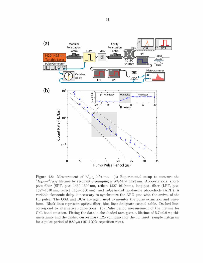
61
101
Co
un
t R
ate
(H
z/b
in)
Pump Pulse Period (µs)
100
10-1
−20 −10 0 10 20 300
4
8
Time (ns)
0 5 10 15 20 25 30 35
Nth pulse(N -1)th decay Nth decayC
ou
nt
Ra
te
OSA
1420-1495 nm
Tunable Laser
Cavity
Polarization
Control
Disk
Taper
VOA
CM
R
P
SPF
CM
R
P
LPF
CM
R
P
LPF
Modulor
Polarization
Control
10 : 90splitter
DCA10%
Histogrammer
1
0
Pulse GeneratorSYNC OUT
Variable
Delay APD
(a)
(b)
EOM
Figure 4.8: Measurement of 4I13/2 lifetime. (a) Experimental setup to measure the4I13/2→4I15/2 lifetime by resonantly pumping a WGM at 1473 nm. Abbreviations: short-pass filter (SPF, pass 1460–1500 nm, reflect 1527–1610 nm), long-pass filter (LPF, pass1527–1610 nm, reflect 1455–1500 nm), and InGaAs/InP avalanche photodiode (APD). Avariable electronic delay is necessary to synchronize the APD gate with the arrival of thePL pulse. The OSA and DCA are again used to monitor the pulse extinction and wave-form. Black lines represent optical fiber; blue lines designate coaxial cable. Dashed linescorrespond to alternative connections. (b) Pulse period measurement of the lifetime forC/L-band emission. Fitting the data in the shaded area gives a lifetime of 5.7±0.9 µs; thisuncertainty and the dashed curves mark ±2σ confidence for the fit. Inset: sample histogramfor a pulse period of 9.89 µs (101.1 kHz repetition rate).
62
arrival of a pump pulse in the detection window simultaneously acquires the PL’s rise and
initial decay due to the Nth pulse along with the decay associated with the (N−1)th pulse.
The appearance of the Nth pulse serves as a marker for sampling the (N − 1)th decay
curve at a fixed delay—i.e., the pulse period separates the (N − 1)th peak from its tail just
before the Nth pulse. Several histograms (128 ps/bin resolution) with varying delays are
used to construct the fluorescence decay in Fig. 4.8. Background histograms are taken at
each point without the pulses to remove dark counts and PL counts from when the pump
is nominally “off”—with –35 dB extinction, the CW excitation is 6.9 nW. As the pulse pe-
riod approaches the PL lifetime, the data deviates from a single exponential curve because
decay from multiple pulses contributes to the PL tail prior to the Nth pulse’s arrival. Data
at longer periods is limited by a constant noise floor linked to the small portion of pump
laser spontaneous emission that is not blocked by the filters. For τeff ≈ 10µs, probabilistic
simulation suggests that a fitting region between 10 and 20µs gives the greatest confidence
unbiased estimate of the decay lifetime. Fitting the points in this range gives an effective
lifetime of 5.7±0.9 µs for a peak excitation of 21.7 µW and ±2σ uncertainty. With the ef-
fective lifetime much lower than the measured 8±0.5 ms (7.8±2.2 ms calculated) radiative
lifetime in lightly Er3+-doped bulk Y2O3 [192], nonradiative relaxation is a major concern.
The nonradiative decay of rare-earth ions was extensively investigated during the early
development of inorganic gain crystals for solid-state lasers, and accurate phenomenologi-
cal models have been established to describe the two principal mechanisms: multiphonon
relaxation and cooperative relaxation (also known as concentration quenching) [193]. First
considering multiphonon emission, the high yield of the 4I13/2→4I15/2 transition in low Er3+-
density samples is because the 0.8 eV (6500 cm−1) energy gap is too large for fast depopula-
tion. Using parameters from Er3+ relaxation in Y2O3 at low temperature [192,194] and the
close similarity of the Er2O3 and Y2O3 vibrational spectra [195], we estimate an effective
lifetime of 4.2 s for relaxation at 300 K via emission of 12 phonons (∼550 cm−1). Coopera-
tive relaxation encompasses several decay and sensitizing mechanisms where the excitation
is nonradiatively transfered between ions through multipole or exchange interactions—we
will limit the discussion to processes involving a single ion species. Self-quenching, where a
donor ion decays to an intermediate level by exciting a low-level transition in a neighbor,
is significant for higher levels in Er3+ (e.g., 4S3/2) [196], but it is inactive for the first ex-
achieved using a 10% detection probability (lower dark counts) and a 5µs dead time (less afterpulsing).
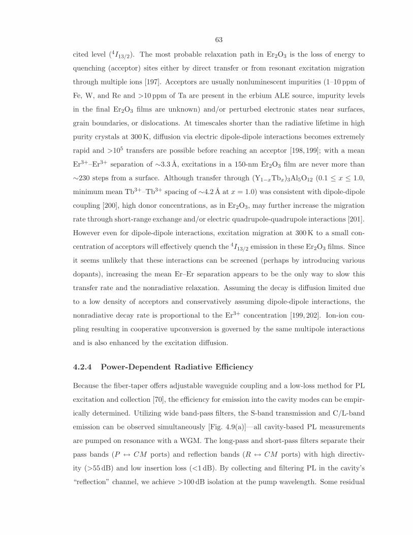
63
cited level (4I13/2). The most probable relaxation path in Er2O3 is the loss of energy to
quenching (acceptor) sites either by direct transfer or from resonant excitation migration
through multiple ions [197]. Acceptors are usually nonluminescent impurities (1–10 ppm of
Fe, W, and Re and >10 ppm of Ta are present in the erbium ALE source, impurity levels
in the final Er2O3 films are unknown) and/or perturbed electronic states near surfaces,
grain boundaries, or dislocations. At timescales shorter than the radiative lifetime in high
purity crystals at 300 K, diffusion via electric dipole-dipole interactions becomes extremely
rapid and >105 transfers are possible before reaching an acceptor [198, 199]; with a mean
Er3+–Er3+ separation of ∼3.3 A, excitations in a 150-nm Er2O3 film are never more than
∼230 steps from a surface. Although transfer through (Y1−xTbx)3Al5O12 (0.1 ≤ x ≤ 1.0,
minimum mean Tb3+–Tb3+ spacing of ∼4.2 A at x = 1.0) was consistent with dipole-dipole
coupling [200], high donor concentrations, as in Er2O3, may further increase the migration
rate through short-range exchange and/or electric quadrupole-quadrupole interactions [201].
However even for dipole-dipole interactions, excitation migration at 300 K to a small con-
centration of acceptors will effectively quench the 4I13/2 emission in these Er2O3 films. Since
it seems unlikely that these interactions can be screened (perhaps by introducing various
dopants), increasing the mean Er–Er separation appears to be the only way to slow this
transfer rate and the nonradiative relaxation. Assuming the decay is diffusion limited due
to a low density of acceptors and conservatively assuming dipole-dipole interactions, the
nonradiative decay rate is proportional to the Er3+ concentration [199, 202]. Ion-ion cou-
pling resulting in cooperative upconversion is governed by the same multipole interactions
and is also enhanced by the excitation diffusion.
4.2.4 Power-Dependent Radiative Efficiency
Because the fiber-taper offers adjustable waveguide coupling and a low-loss method for PL
excitation and collection [70], the efficiency for emission into the cavity modes can be empir-
ically determined. Utilizing wide band-pass filters, the S-band transmission and C/L-band
emission can be observed simultaneously [Fig. 4.9(a)]—all cavity-based PL measurements
are pumped on resonance with a WGM. The long-pass and short-pass filters separate their
pass bands (P ↔ CM ports) and reflection bands (R ↔ CM ports) with high directiv-
ity (>55 dB) and low insertion loss (<1 dB). By collecting and filtering PL in the cavity’s
“reflection” channel, we achieve >100 dB isolation at the pump wavelength. Some residual
64
spontaneous emission from the laser diode does bleed through the filters and produces a
∼10 pW signal at 1519 nm with our pump near maximum power. Since the radiative effi-
ciency measurements only concern WGMs at λ > 1520 nm, this peak is ignored; in other
cases it can be reduced below 1 pW by inserting an additional short-pass filter (pass 1450–
1495 nm) after the laser. We employ an optical spectrum analyzer to measure the PL at
peak powers &10 pW and a spectrometer with a liquid-N2 cooled InGaAs detector array at
lower powers (down to peak powers of ∼0.1 fW).
The cavity-coupled radiative efficiency (ηobs) is given by the ratio of the total power
emitted into the cavity modes divided by the absorbed pump power. This measurement
requires careful characterization of the pump mode along with all modes in the desired
emission band. For these c-Er2O3 microdisks, surface scattering and radiation losses are
negligible compared to the Er3+ absorption, and the absorbed power (Pa) is nearly equal
to the dropped power (Pd),
Pa =γa
γiPd ≈ Pd = (1 − Tcav)
Pin√Tt, (4.4)
where Tcav is the cavity-waveguide transmission at the pump wavelength, Tt is the end-
to-end fiber-taper transmission, and Pin is the pump power measured at the fiber-taper
input. Equation 4.4 assumes the taper’s loss is symmetric about the taper-device coupling
region. While transmission loss in fiber-tapers is usually dominated by bending loss in the
taper mount which is symmetric about the coupling region, small bits of dust on the taper
will scatter light from the fundamental mode and produce asymmetric loss. In this case,√Tt is replaced by the one-sided waveguide transmission (T1), which can be found from
Tt and the ratio of another quantity that depends on Pd (e.g., thermo-optic wavelength
shift or peak PL yield) when using either end of the waveguide as the input. For these
measurements, Tt = 0.68 with symmetric loss. Using the collected emission [P (λ)] spectrum
as in Fig. 4.9(b), the total power emitted into the cavity modes (Pcav) is given by
Pcav =2
δλrbw
√Tt
[
∑
n
(
γi,n + γe,n
γe,n
)∫
Pn(λ)
Tf(λ)dλ
]
, (4.5)
where the summation is over the cavity modes at λ > 1520 nm and δλrbw is the spectral
resolution bandwidth of the grating and detector. The factor of 2 compensates for equal
65
5x10⁻⁵
Absorbed Power (W)
Ob
serv
ed
Ca
vit
y E
ffic
ien
cy (η
ob
s)
10-5
10-9 10-8 10-7 10-6 10-5 10-4 10-3 10-2
observed ≈ 3.4×10⁻⁵
Ov
era
ll Efficie
ncy (η
scl )
2x10⁻⁴
overall ≈ 9.0×10⁻⁴
taper
Er2O3 disk edge
Si pedestal edge
10-3
10 µm
OSA
1420-1495 nm
Tunable Laser
FPC
Disk
TaperPD
Trans
VOAVOA
CM
R
P
SPF
CM
R
P
LPF
CM
R
P
LPF
IR Spectrometer
InGaAs
CCD
(a)
(c)Wavelength (nm)
Co
llect
ed
PL
(p
W)
1520 1540 1560 1580 1600 1620 1640 1660 1680 17000
80
120
160
40
200
Pump Mode:
1st order
2nd order
(b)
Figure 4.9: (a) Setup for measuring C/L-band PL and ηobs. (b) Observed cavity-coupledPL for the device in Fig. 4.4; the TEp=1 modes are highlighted in gray. (c) Power-dependentradiative efficiency of the 4I13/2→4I15/2 transition. The marker color indicates the pump-mode wavelength from blue (1460.9 nm) to dark red (1494.5 nm) while () and (+) designatefirst- and second-order radial pump modes, respectively. Black markers represent datafrom devices on another wafer processed with wet chemical etching and using first- andsecond-order pump modes (spanning 1437.6–1490.9 nm). The inset shows green upconvertedluminescence from a TEp=1 mode [35].
66
emission into the degenerate clockwise and counterclockwise traveling-wave modes of the
disk and hence into the forward- and backward-propagating modes of the waveguide. While
the C/L-band transmission [Tf(λ)] is fairly flat for the filters used to (de)multiplex the PL
and the pump beam, the transmission does slowly decrease at longer wavelengths. In the
emission band, Tt = 0.66 with symmetric loss. To establish and correct for the fraction of
the PL in the WGMs that is collected by the taper, we find the total cavity loss rate for
each cavity mode in the emission band by measuring the γi,n under weak loading and γe,n
at the fixed taper position used during PL collection. Then the fraction of Pcav coupled into
the forward propagating mode is the ratio of the loss rate into the waveguide (γe,n) over the
loss rate into all channels (γi,n + γe,n), which gives a correction factor of (γi,n + γe,n)/γe,n.
There is no evidence for significant parasitic loading (γp ≈ 0) during this measurement.
For example, the WGMs near the emission peaks at 1535 and 1549 nm are nearly critically
coupled in Fig. 4.4 (γi,n ≈ γe,n), and the waveguide collection factor for these modes is
(γi,n + γe,n)/γe,n ≈ 2. Since the ratio of the intensity of individual WGMs over the total
emitted power is constant at Pd . 4mW, the total integrated PL is proportional to the
intensity of the strongest emission line. Using this proportionality, the radiative efficiency
measurement can be extended to excitation levels low enough that the largest PL peak is
just above the noise floor.
We analyze the power dependence of ηobs for several pump modes across the S-band on
two different samples. In Fig. 4.9, ηobs decreases as upconversion becomes the dominant
path for depopulating 4I13/2. Fitting the data to
ηobs(Pa) =ηo
1 + (Pa/Pup)x(4.6)
gives x = 0.61±0.07 and Pup = 204±47 µW, at which point the efficiency has dropped by
half and there are equal rates for nonradiative relaxation and cooperative upconversion.
Expressed in terms of an effective lifetime (τeff) and the state’s lifetime at zero pump power
(τo)
τeff(Pa) = τo(
1 + (Pa/Pup)x)
, (4.7)
residual upconversion can be removed from the previous lifetime estimate of 5.7±0.9 µs at
21.7 µW to give a zero-power effective 4I13/2 lifetime of τo = 7.2±1.2 µs. Since the radiative
lifetime (τrad) in these Er2O3 films should be very similar to the 8 ms lifetime in Y2O3 [192],
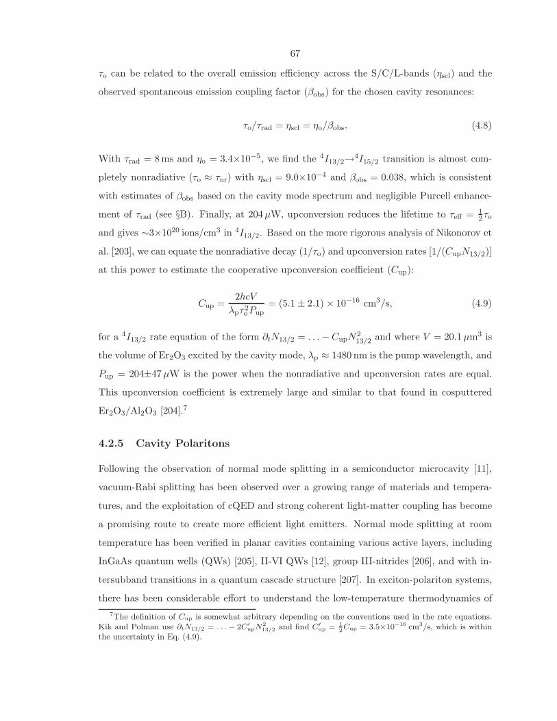
67
τo can be related to the overall emission efficiency across the S/C/L-bands (ηscl) and the
observed spontaneous emission coupling factor (βobs) for the chosen cavity resonances:
τo/τrad = ηscl = ηo/βobs. (4.8)
With τrad = 8 ms and ηo = 3.4×10⁻⁵, we find the 4I13/2→4I15/2 transition is almost com-
pletely nonradiative (τo ≈ τnr) with ηscl = 9.0×10⁻⁴ and βobs = 0.038, which is consistent
with estimates of βobs based on the cavity mode spectrum and negligible Purcell enhance-
ment of τrad (see §B). Finally, at 204µW, upconversion reduces the lifetime to τeff = 12τo
and gives ∼3×10²⁰ ions/cm3 in 4I13/2. Based on the more rigorous analysis of Nikonorov et
al. [203], we can equate the nonradiative decay (1/τo) and upconversion rates [1/(CupN13/2)]
at this power to estimate the cooperative upconversion coefficient (Cup):
Cup =2hcV
λpτ2oPup
= (5.1 ± 2.1) × 10−16 cm3/s, (4.9)
for a 4I13/2 rate equation of the form ∂tN13/2 = . . .−CupN213/2 and where V = 20.1 µm3 is
the volume of Er2O3 excited by the cavity mode, λp ≈ 1480 nm is the pump wavelength, and
Pup = 204±47 µW is the power when the nonradiative and upconversion rates are equal.
This upconversion coefficient is extremely large and similar to that found in cosputtered
Er2O3/Al2O3 [204].7
4.2.5 Cavity Polaritons
Following the observation of normal mode splitting in a semiconductor microcavity [11],
vacuum-Rabi splitting has been observed over a growing range of materials and tempera-
tures, and the exploitation of cQED and strong coherent light-matter coupling has become
a promising route to create more efficient light emitters. Normal mode splitting at room
temperature has been verified in planar cavities containing various active layers, including
InGaAs quantum wells (QWs) [205], II-VI QWs [12], group III-nitrides [206], and with in-
tersubband transitions in a quantum cascade structure [207]. In exciton-polariton systems,
there has been considerable effort to understand the low-temperature thermodynamics of
7The definition of Cup is somewhat arbitrary depending on the conventions used in the rate equations.Kik and Polman use ∂tN13/2 = . . . − 2C′
upN213/2 and find C′
up = 12Cup = 3.5×10⁻¹⁶ cm3/s, which is within
the uncertainty in Eq. (4.9).
68
the boson quasiparticles and to utilize stimulated scattering toward the lower polariton
branch [208, 209]. Optoelectronic functionalities based on efficient polariton emission from
single excitons, such as parametric gain [210] and electroluminescence (EL) [211,212], have
now also progressed above T & 200 K.
Rabi splitting and the associated cavity-polariton modes can be described as a conse-
quence of linear dispersion [213] or as non-perturbative coupling between the dipole(s) and
an optical cavity, while perturbative coupling to a single ion produces Purcell-enhanced
emission (without Rabi oscillation) [214]. Beyond quantum wells and single dipoles with
large oscillator strengths, the collective oscillation of atomic and molecular ensembles is
another viable method to obtaining light from polariton states. Due to their large dipole
moment, planar microcavities incorporating organic semiconductor emitters exhibit massive
room-temperature Rabi splitting [215] and EL [216]. While in a complementary approach
with high density (ρ = 2.7×1022 cm−3), the narrow inhomogeneous distribution of optical
transitions in stoichiometric erbium crystals can also intrinsically produce large dispersive
resonances in the refractive index and splitting of the cavity modes. Cavity polaritons have
been observed around a single Er3+ transition in polycrystalline Er2O3 produced by sput-
tering or oxidation of an erbium film [217], but the effect was quenched at T & 40 K [218].
In this section, we analyze the properties of low temperature (T ≈ 8K) and high temper-
ature (T > 361 K) cavity-polaritons formed between the microdisk WGMs and the Er3+
4I13/2↔4I15/2 transitions in epitaxial Er2O3-on-Si.8
Analyzing the polariton response involves continuously tuning a cavity mode across
the Er3+ transitions. As a mode is shifted through an optical transition, the resonances
anticross (i.e., the vacuum-Rabi splitting) and produce symmetric hybrid modes (i.e., the
cavity-polaritons), which appear in both the cavity transmission and PL. In terms of cQED,
the fundamental quantity for cavity-polaritons is the Rabi frequency that describes the
coherent coupling between the two-level system(s) and a near-resonant optical mode. For
a uniform distribution of emitters, the many-dipole Rabi frequency (gN ) is given by
|gN |2 = N |g1|2 ≈ |~µ|2ωcρΓ
2ℏn2ǫ0, (4.10)
where g1 is the mean coupling rate experienced by a single dipole, N is the number of
8Reprinted with permission from Appl. Phys. Lett. 94, 131103 (2009). Copyright 2009, American Insti-tute of Physics.
69
dipoles in the cavity, ~µ is the electric dipole moment of the optical transition, ωc (λc)
is frequency (wavelength) of the cavity resonance, n is the refractive index of the dipole
medium, ρ ≈ N/(VeffΓ) is the dipole density in Er2O3, Veff ≈ 70(λc/n)3 is the optical mode
volume from Eq. (1.28), and Γ is the optical mode’s electric-field energy overlap with the
dipole ensemble from Eq. (1.29) [6, 219]—see also §A.4. In Er2O3 resonators, a large Er3+
density overcomes the small 4I13/2→4I15/2 dipole moment to produce resolved polariton
modes.
4.2.5.1 Low-Temperature Polaritons
Measurements at cryogenic temperatures are conducted in a continuous flow 4He cryostat
with the fiber-taper waveguide and sample mounted on piezoelectric stages with a base
temperature of 8 K. At cryogenic temperatures, the homogeneous linewidths of the Er3+
transitions narrow significantly, and 99.8% of the ions reside in the Z1 sublevel of 4I15/2
(compared to 24.3% at 300 K). As in Fig. 4.5(a), the observed linewidths are due to inho-
mogeneous broadening from ions in strained volumes or near dislocations. To study the
polariton modes, the repeatable deposition and sublimation of thick N2 films (n ≈ 2) can
tune the Er2O3 cavity modes more than 25 nm. Compared to GaAs disks which only tune
up to 4 nm [220], the Er2O3 resonators are thinner with lower refractive index. The addi-
tional scattering loss due to the roughness of the N2 ice also remains negligible compared
to the resonant Er3+ absorption. Away from the Er3+ transitions, the dominant sources
of loss are surface scattering at the milled sidewalls and parasitic coupling from the fiber-
taper.9 Testing the cavity transmission over a range from 1423 to 1625 nm, we measure
nine anticrossings between 1455.5 and 1548.6 nm (Fig. 4.10). Considering Rabi splitting
within the context of linear absorption [213], we expect that polaritons will form at 8K
around transitions originating from the lowest sublevel (Z1) of 4I15/2, and we observe split-
ting about excitations from Z1 to all seven Stark sublevels (Y1−7) of 4I13/2 on the C2 lattice
sites—the inhomogeneous distributions for the Y3 and Y4 sublevels overlap around 1516 nm.
Rabi splitting also occurs about three transitions (Z ′1→Y ′
1−3) on the C3i sites. Table 4.2
summarizes the average measured Rabi splittings (δωvrs) and the transition linewidth (∆ω)
9These measurements were conducted during a period when many tapers were breaking in the cryostat.This problem was likely due to large thermal gradients when the fiber was placed in contact with thesample. One solution was to use larger, more robust tapers, but the final resolution was to wait longer forthe temperatures to equilibrate.
70
N2
Exp
osu
re T
ime
(a
rb. u
nit
s)
Wavelength (nm)
20
60
100
140
1430 1440 1450 1460 1470 1480 1490
1510 1520 1530 1540 1550
20
60
100
140
1545153515251515
1525 1530 1535 1540 1545 1550 1555
10
20
30
40
50
60 (c)
Cavity ModesEr3+ Transitions
Co
un
ts (arb
. un
its)
0.0
0.2
0.4
0.6
0.8
1.0
Tra
nsm
ission
0.0
0.2
0.4
0.6
0.8
1.0
(a)
(b)
1510 1520 1530 1540 1550 1560 1570 1580 1590
250
200
150
100
50PL
(a
rb. u
nit
s)
Y3–Z
1 (
C3
i)
Y2–Z
1 (
C2)
Y1–Z
1 (
C2)
Y2–Z
2 (
C2)
Y2–Z
1 (
C3
i) o
r Y
1–Z
2 (
C2)
Y1–Z
1 (
C3
i)
Y3–Z
3 (
C3
i)
Y1–Z
3 (
C2)
Y1–Z
4 (
C2)
Y2–Z
3 (
C3
i)
Y1–Z
5 (
C2)
Y1–Z
3? (
C3
i)
(d)
740 2,300 13,000
Figure 4.10: Cavity transmission spectra in the (a) S-band and (b) C-band at 8.6 K tunedusing N2 deposition. The shallow background ripple is residual-etalon noise from the tunablelasers or ringing from the notch filters used to filter out that noise. (c) Taper-collected PLspectrum as the cavity is tuned. Equal spaced contours (∆ = 0.002) are used to displaylow-intensity features. The Er3+ ions are excited by resonantly pumping a WGM near1480 nm. (d) Identified transitions in the bulk PL spectrum at 8.6 K.
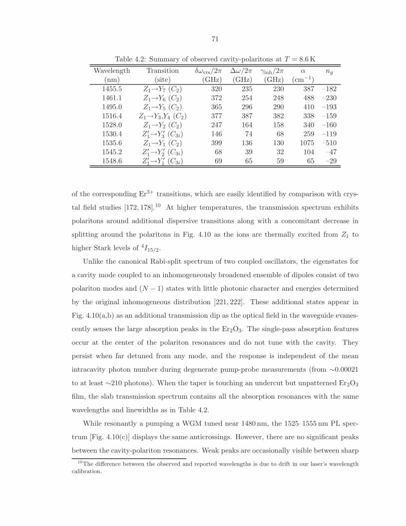
71
Table 4.2: Summary of observed cavity-polaritons at T = 8.6 K
Wavelength Transition δωvrs/2π ∆ω/2π γinh/2π α ng
(nm) (site) (GHz) (GHz) (GHz) (cm−1)
1455.5 Z1→Y7 (C2) 320 235 230 387 –1821461.1 Z1→Y6 (C2) 372 254 248 488 –2301495.0 Z1→Y5 (C2) 365 296 290 410 –1931516.4 Z1→Y3,Y4 (C2) 377 387 382 338 –1591528.0 Z1→Y2 (C2) 247 164 158 340 –1601530.4 Z ′
1→Y ′3 (C3i) 146 74 68 259 –119
1535.6 Z1→Y1 (C2) 399 136 130 1075 –5101545.2 Z ′
1→Y ′2 (C3i) 68 39 32 104 –47
1548.6 Z ′1→Y ′
1 (C3i) 69 65 59 65 –29
of the corresponding Er3+ transitions, which are easily identified by comparison with crys-
tal field studies [172, 178].10 At higher temperatures, the transmission spectrum exhibits
polaritons around additional dispersive transitions along with a concomitant decrease in
splitting around the polaritons in Fig. 4.10 as the ions are thermally excited from Z1 to
higher Stark levels of 4I15/2.
Unlike the canonical Rabi-split spectrum of two coupled oscillators, the eigenstates for
a cavity mode coupled to an inhomogeneously broadened ensemble of dipoles consist of two
polariton modes and (N − 1) states with little photonic character and energies determined
by the original inhomogeneous distribution [221, 222]. These additional states appear in
Fig. 4.10(a,b) as an additional transmission dip as the optical field in the waveguide evanes-
cently senses the large absorption peaks in the Er2O3. The single-pass absorption features
occur at the center of the polariton resonances and do not tune with the cavity. They
persist when far detuned from any mode, and the response is independent of the mean
intracavity photon number during degenerate pump-probe measurements (from ∼0.00021
to at least ∼210 photons). When the taper is touching an undercut but unpatterned Er2O3
film, the slab transmission spectrum contains all the absorption resonances with the same
wavelengths and linewidths as in Table 4.2.
While resonantly a pumping a WGM tuned near 1480 nm, the 1525–1555 nm PL spec-
trum [Fig. 4.10(c)] displays the same anticrossings. However, there are no significant peaks
between the cavity-polariton resonances. Weak peaks are occasionally visible between sharp
10The difference between the observed and reported wavelengths is due to drift in our laser’s wavelengthcalibration.
72
>10× stronger cavity-polariton lines, but these peaks are due to spontaneous emission from
a small number of excited ions that is collected by the nearby taper. The tuned PL spectra
also reveal transitions that do not terminate in the lowest sublevels. At 1553.9 nm, the
Y1→Z3 (C2 site) emission is barely detectable above the noise floor unless resonant with
a WGM. The data in Fig. 4.10 reflect the trend in Fig. 4.5 and 4.10(d) where emission
from ions on C3i sites is disproportionately large relative to the C3i absorption and the
C2 emission. To illustrate this point without rigorous calculations, the polariton splitting
[per ion, using the√N dependence in Eq. (4.10)] at the Z1→Y1 line on both sites roughly
follows the absorption cross sections (σa) calculated for erbium-doped Y2O3 [178]
δωC2vrs√NC2
= 3.3
(
δωC3ivrs√NC3i
)
and σC2a = 4.8σC3i
a ,
as expected under weak pumping. However, the Y1→Z1 emission (per ion) in Fig. 4.10(d)
at 8 K deviates significantly from the emission cross sections (σe) obtained for both sites:
PC2
NC2
= 0.02
(
PC3i
NC3i
)
and σC2e = 1.04σC3i
e .
As discussed previously, a possible explanation for the emission behavior is asymmetric exci-
tation transfer between the 4I13/2 levels on the C2 and C3i sites. The interion diffusion rate
slows at low temperature because the thermal occupancy of the Stark levels limits the paths
that can participate (any nonresonant transfers require phonons to conserve energy), but
resonant transfer through the lowest sublevels is always active. One mechanism that may
contribute to this asymmetry is the misalignment of the Y1 and Y ′1 sublevels. The different
crystal fields at the C2 and C3i sites can split identical sublevels between 3 and 240 cm−1
(mean absolute shift of 65 cm−1 = 8.1 meV) [177],11 and if the Y1 level is higher, excitations
transferred to the C3i sublattice may encounter a sizable energy barrier for returning to
the C2 ions (kBT = 0.74 meV at 8.6 K). The PL peak at 1545.1 nm in Fig. 4.10(d) com-
plicates this argument because it contains contributions from two unresolved transitions:
Y1→Z2 (C2, nominally 1544.7 nm) and Y ′2→Z ′
1 (C3i, nominally 1545.4 nm). If the Y1/Y′1
misalignment is significant, then the emission from the C2 site must dominate at this wave-
length because it has a larger emission cross section in dilute Y2O3. However, the Y1→Z2
11By the nature of the crystal field calculations, the energy levels are found relative to the ground stateand without reference to an absolute scale.
73
cross section is not large enough to account for the disparity with the Y1→Z1 (C2) peak at
1535.5 nm, which is markedly weaker and should have similar amplitude. If emission from
the C3i ions is more intense, another mechanism must be present because it is unlikely that
the Y ′2 level is also shifted significantly below Y1. Temperature-dependent lifetime measure-
ments for the individual transitions would help clarify this matter (as in Ref. [223]); further
information could also be obtained from tertiary alloys such as (Y1−xErx)2O3 similar to the
thorough studies of La1−xErxF3 [202] and (Y1−xTbx)3Al5O12 [200].
The polariton resonances provide useful spectra features for studying the optical tran-
sitions, but the homogeneous (γh) and inhomogeneous linewidths γinh must first be con-
sidered. The homogeneous linewidth (and the dephasing time T2: γh/2π = 1/(πT2)) is
extremely sensitive to the temperature, transition, and host matrix. For example with the
4F9/2→4I15/2 transition in Er3+:YLiF4 at 4.2 K, photon echos by MacFarlane et al. show T2
decreases from >4µs to 0.4 µs when the Er3+ concentration increases from 0.1% to 1% [224].
Without previous studies of dephasing in Er2O3, we conservatively use γh/2π = 10 GHz at
8 K, which is similar to erbium-doped glass [225,226], and we deconvolve γh, γinh from ∆ω
in Table 4.2 using the Voigt profile. Inhomogeneous broadening of quantum well excitons
has been shown to damp the coherent oscillations with the cavity field [227, 228] without
significantly reducing the spectral Rabi splitting [221, 222]. In the limit gN ≫ γinh > γh,
the linewidth of the polariton modes becomes 12 (γℓ + γh), where γℓ is again the loaded
linewidth of the cavity mode. However, this averaging does not occur when gN and γinh are
similar because the cavity mode experiences more absorption and broadens as it approaches
resonance with the optical transition [229]. The magnitudes of γinh, gN in these Er2O3
films is in a regime that gives δωvrs ≈ 2gN and only modest narrowing of the polariton
modes around the most dispersive transitions; we observe line narrowing of ∼20% for the
polaritons at 1535 nm.
Using the observed splitting and Eq. (4.10), we find an effective dipole moment |〈~µ〉|for each cavity polariton and estimate the absorption coefficient (α) and the group index
(ng) under weak excitation. For an ensemble of dipoles interacting with an optical field, the
electromagnetic susceptibility (χ) can be obtained from a density matrix approach by as-
suming the dipoles consist of only two levels (∆E = ℏωo) and including a phenomenological
74
dephasing rate:
χ(ω) ≡ χ′ − iχ′′ =π|~µ|2(ωo − ω)T2
ǫoℏ∆NL(ω) − i
π|~µ|2ǫoℏ
∆NL(ω), (4.11)
where ∆N is the population difference between the two states (per volume) and the ho-
mogeneously broadened lineshape L(ω) = L(ω, ωo, γh) is a Lorentzian with width γh and
normalization such that∫∞
−∞L(ω)dω = 1 [230]. Assuming that the fields are weak and
ℏωo ≫ kBT , the dipoles remain in their ground states, and the frequency- and power-
dependent ∆N equals the dipole density (ρ). Then the propagation constant (β′) for a
monochromatic plane wave ~Eei(ωt−β′z) becomes
β′ ≡ ω√
µoǫ′ ≈ β(
1 +ǫo2ǫχ(ω)
)
. . . for |χ| ≪ 1, (4.12)
where ǫ′ = ǫ + ǫoχ is the complex permittivity, ǫ is the permittivity that accounts for
nonresonant contributions to the medium’s polarization, and β = ω√µoǫ is the propagation
constant in the absence of the two level transition. The change in the refractive index (∆n)
and the intensity absorption coefficient (α) can be found found from the real and imaginary
parts of Eq. (4.12):
∆n
n=
ℜ(β′) − β
β=χ′(ω)
2n2, (4.13)
α = −2ℑ(β′) =βχ′′(ω)
n2, (4.14)
with the refractive index far from the transition is given by n =√
ǫ/ǫo. Strong transitions
with narrow linewidths will also affect the group index:
ng = n+ ω
(
dn
dω
)
≈ n+ω
2n
(
dχ′
dω
)
. . . for |χ| ≪ 1. (4.15)
Equation 4.10 can be combined with the formulas above to simply express the peak ab-
sorption coefficient and group index for a homogeneously broadened transition in terms of
polariton parameters:
α(ωo) =4n|gN |2cγhΓ
and ng(ωo) = n
(
1 − 4|gN |2γ2hΓ
)
. (4.16)
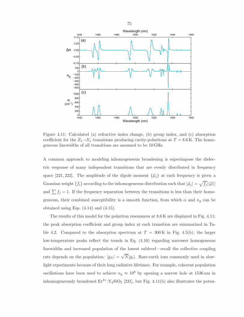
75
−0.10
−0.05
0.00
0.05
0.10
Δn
−500
−400
−300
−200
−100
0
100
1440 1460 1480 1500 1520 1540 15600
200
400
600
800
1000
Wavelength (nm)
1440 1460 1480 1500 1520 1540 1560
Wavelength (nm)
ng
α(cm-1)
(a)
(b)
(c)
Figure 4.11: Calculated (a) refractive index change, (b) group index, and (c) absorptioncoefficient for the Z1→Yx transitions producing cavity-polaritons at T = 8.6 K. The homo-geneous linewidths of all transitions are assumed to be 10 GHz.
A common approach to modeling inhomogeneous broadening is superimpose the dielec-
tric response of many independent transitions that are evenly distributed in frequency
space [221, 222]. The amplitude of the dipole moment ~µj at each frequency is given a
Gaussian weight fi according to the inhomogeneous distribution such that |~µj | =√
fj|〈~µ〉|and
∑
fj = 1. If the frequency separation between the transitions is less than their homo-
geneous, their combined susceptibility is a smooth function, from which α and ng can be
obtained using Eqs. (4.14) and (4.15).
The results of this model for the polariton resonances at 8.6 K are displayed in Fig. 4.11;
the peak absorption coefficient and group index at each transition are summarized in Ta-
ble 4.2. Compared to the absorption spectrum at T = 300 K in Fig. 4.5(b), the larger
low-temperature peaks reflect the trends in Eq. (4.16) regarding narrower homogeneous
linewidths and increased population of the lowest sublevel—recall the collective coupling
rate depends on the population: |gN | =√N |g1|. Rare-earth ions commonly used in slow-
light experiments because of their long radiative lifetimes. For example, coherent population
oscillations have been used to achieve ng ≈ 108 by opening a narrow hole at 1536 nm in
inhomogeneously broadened Er3+:Y2SiO5 [231], but Fig. 4.11(b) also illustrates the poten-
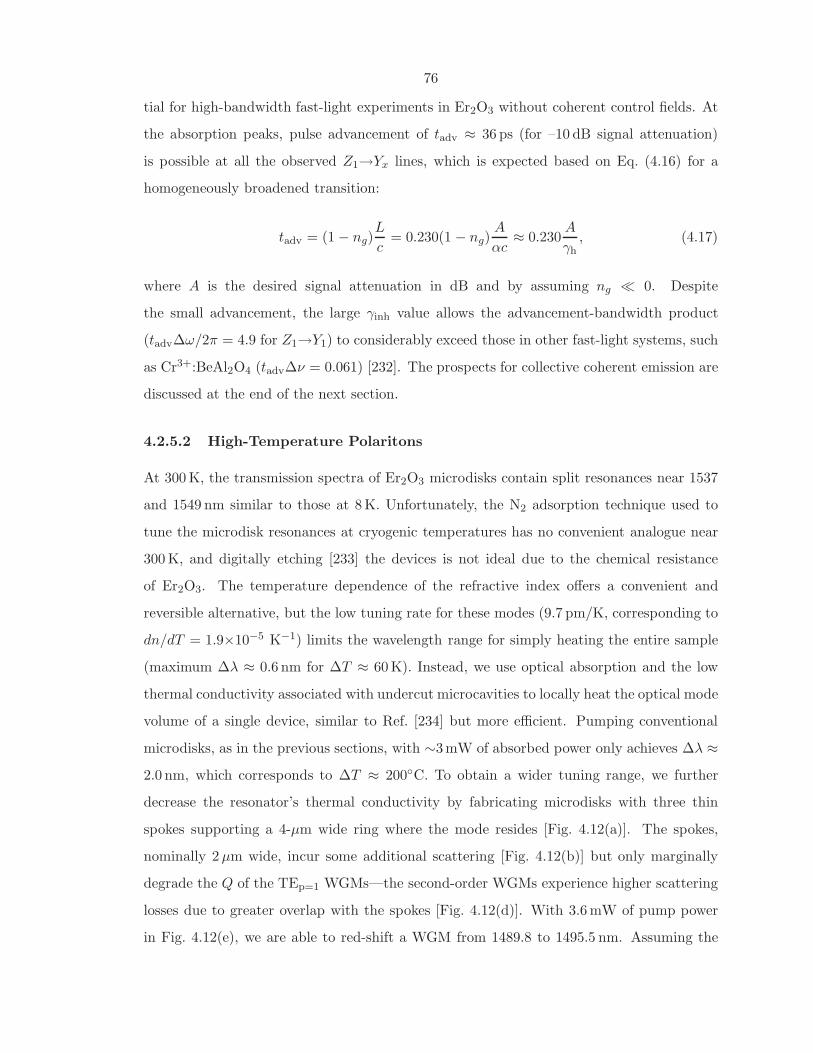
76
tial for high-bandwidth fast-light experiments in Er2O3 without coherent control fields. At
the absorption peaks, pulse advancement of tadv ≈ 36 ps (for –10 dB signal attenuation)
is possible at all the observed Z1→Yx lines, which is expected based on Eq. (4.16) for a
homogeneously broadened transition:
tadv = (1 − ng)L
c= 0.230(1 − ng)
A
αc≈ 0.230
A
γh, (4.17)
where A is the desired signal attenuation in dB and by assuming ng ≪ 0. Despite
the small advancement, the large γinh value allows the advancement-bandwidth product
(tadv∆ω/2π = 4.9 for Z1→Y1) to considerably exceed those in other fast-light systems, such
as Cr3+:BeAl2O4 (tadv∆ν = 0.061) [232]. The prospects for collective coherent emission are
discussed at the end of the next section.
4.2.5.2 High-Temperature Polaritons
At 300 K, the transmission spectra of Er2O3 microdisks contain split resonances near 1537
and 1549 nm similar to those at 8 K. Unfortunately, the N2 adsorption technique used to
tune the microdisk resonances at cryogenic temperatures has no convenient analogue near
300 K, and digitally etching [233] the devices is not ideal due to the chemical resistance
of Er2O3. The temperature dependence of the refractive index offers a convenient and
reversible alternative, but the low tuning rate for these modes (9.7 pm/K, corresponding to
dn/dT = 1.9×10⁻⁵ K−1) limits the wavelength range for simply heating the entire sample
(maximum ∆λ ≈ 0.6 nm for ∆T ≈ 60 K). Instead, we use optical absorption and the low
thermal conductivity associated with undercut microcavities to locally heat the optical mode
volume of a single device, similar to Ref. [234] but more efficient. Pumping conventional
microdisks, as in the previous sections, with ∼3mW of absorbed power only achieves ∆λ ≈2.0 nm, which corresponds to ∆T ≈ 200C. To obtain a wider tuning range, we further
decrease the resonator’s thermal conductivity by fabricating microdisks with three thin
spokes supporting a 4-µm wide ring where the mode resides [Fig. 4.12(a)]. The spokes,
nominally 2µm wide, incur some additional scattering [Fig. 4.12(b)] but only marginally
degrade the Q of the TEp=1 WGMs—the second-order WGMs experience higher scattering
losses due to greater overlap with the spokes [Fig. 4.12(d)]. With 3.6 mW of pump power
in Fig. 4.12(e), we are able to red-shift a WGM from 1489.8 to 1495.5 nm. Assuming the
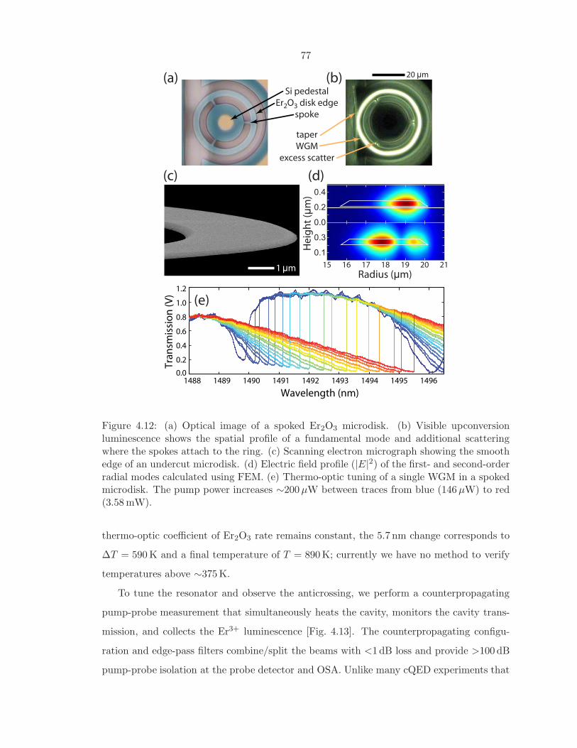
77
20 μm(a) (b)
1 μm 15 16 17 18 19 20 21
Radius (μm)
0.0
0.3
0.1
0.2
0.4
He
igh
t (μ
m)
(d)(c)
Si pedestal
Er2O3 disk edge
spoke
taper
WGM
excess scatter
1488 1489 1490 1491 1492 1493 1494 1495 14960.0
0.2
0.4
0.6
0.8
1.0
1.2
Wavelength (nm)
Tra
nsm
issi
on
(V
)
(e)
Figure 4.12: (a) Optical image of a spoked Er2O3 microdisk. (b) Visible upconversionluminescence shows the spatial profile of a fundamental mode and additional scatteringwhere the spokes attach to the ring. (c) Scanning electron micrograph showing the smoothedge of an undercut microdisk. (d) Electric field profile (|E|2) of the first- and second-orderradial modes calculated using FEM. (e) Thermo-optic tuning of a single WGM in a spokedmicrodisk. The pump power increases ∼200µW between traces from blue (146µW) to red(3.58 mW).
thermo-optic coefficient of Er2O3 rate remains constant, the 5.7 nm change corresponds to
∆T = 590 K and a final temperature of T = 890 K; currently we have no method to verify
temperatures above ∼375 K.
To tune the resonator and observe the anticrossing, we perform a counterpropagating
pump-probe measurement that simultaneously heats the cavity, monitors the cavity trans-
mission, and collects the Er3+ luminescence [Fig. 4.13]. The counterpropagating configu-
ration and edge-pass filters combine/split the beams with <1 dB loss and provide >100 dB
pump-probe isolation at the probe detector and OSA. Unlike many cQED experiments that
78
SpectrumAnalyzer
PolarizationController
1420 - 1495 nm
Pump Laser
1495 - 1565 nm
Probe Laser
VariableOptical
Attenuator
Disk
Taper
Short-Pass Filter(pass 1460-1500 nm,
reflect 1527-1610 nm)
PumpDetector
50 : 50splitter
ProbeDetector
CMR
P
CM R
P
Short-Pass Filter
Long-Pass Filter(pass 1527-1610 nm,
reflect 1455-1500 nm)
PolarizationController
CM R
P
Figure 4.13: Schematic layout for polariton pump-probe measurements.
must minimize Veff , the uniform dipole density for planar microdisks [see Eq. (4.10)] makes
gN independent of Veff so Γ and ρ become more important design parameters. For these
experiments, a microdisk radius of ∼20µm is again chosen so the quasi-TE mode spectrum
consists of evenly spaced first- and second-order radial modes—Γ = 0.67 and has a weak
dependence on radius. This radius is also chosen because the FSR between modes of a single
family is approximately equal to the separation of the polaritons (∆λ ≈ 12 nm) so the cavity
can be tuned onto resonance simultaneously with both transitions. The cavities’ radii are
also varied slightly to acquire a device with first-order WGMs slightly blue detuned from
the polariton features at 1537 and 1549 nm. With the fiber-taper input/collection waveg-
uide in contact with the disk to stabilize the coupling against mechanical noise, we pump
a fundamental WGM near 1490 nm with 0.5 to 2.5 mW in the clockwise direction to heat
the disk and drive the 4I13/2↔4I15/2 transition. While the 1490-nm pump laser is tuned
to maximize the dropped pump power, a second ∼200 nW tunable laser probes the cavity’s
transmission spectrum in the counterclockwise direction. The C-band PL is also measured
by simply blocking this probe beam.
As the cavity is heated, the split resonances clearly anticross in both transmission
[Fig. 4.14(a)] and PL [Fig. 4.14(b)] while the bare cavity modes tune as a quadratic poly-
nomial of the pump power—the nonlinearity stems from Er3+ cooperative upconversion
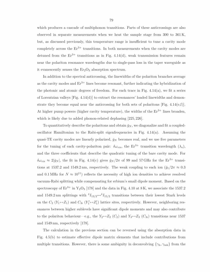
79
which produces a cascade of multiphonon transitions. Parts of these anticrossings are also
observed in separate measurements when we heat the sample stage from 300 to 361 K,
but, as discussed previously, this temperature range is insufficient to tune a cavity mode
completely across the Er3+ transitions. In both measurements when the cavity modes are
detuned from the Er3+ transitions as in Fig. 4.14(d), weak transmission features remain
near the polariton resonance wavelengths due to single-pass loss in the taper waveguide as
it evanescently senses the Er2O3 absorption spectrum.
In addition to the spectral anticrossing, the linewidths of the polariton branches average
as the cavity modes and Er3+ lines become resonant, further indicating the hybridization of
the photonic and atomic degrees of freedom. For each trace in Fig. 4.14(a), we fit a series
of Lorentzian valleys [Fig. 4.14(d)] to extract the resonances’ loaded linewidths and demon-
strate they become equal near the anticrossing for both sets of polaritons [Fig. 4.14(e,f)].
At higher pump powers (higher cavity temperature), the widths of the Er3+ lines broaden,
which is likely due to added phonon-related dephasing [225,226].
To quantitatively describe the polaritons and obtain gN , we diagonalize and fit a coupled-
oscillator Hamiltonian to the Rabi-split eigenfrequencies in Fig. 4.14(a). Assuming the
quasi-TE cavity modes are linearly polarized, gN becomes real, and we use five parameters
for the tuning of each cavity-polariton pair: δωvrs, the Er3+ transition wavelength (λo),
and the three coefficients that describe the quadratic tuning of the bare cavity mode. For
δωvrs ≈ 2|gN |, the fit in Fig. 4.14(c) gives gN/2π of 99 and 57 GHz for the Er3+ transi-
tions at 1537.2 and 1549.2 nm, respectively. The weak coupling to each ion (g1/2π ≈ 0.3
and 0.1 MHz for N ≈ 1011) reflects the necessity of high ion densities to achieve resolved
vacuum-Rabi splitting while compensating for erbium’s small dipole moment. Based on the
spectroscopy of Er3+ in Y2O3 [178] and the data in Fig. 4.10 at 8 K, we associate the 1537.2
and 1549.2 nm splittings with 4I13/2↔4I15/2 transitions between their lowest Stark levels
on the C2 (Y1↔Z1) and C3i (Y ′1↔Z ′
1) lattice sites, respectively. However, neighboring res-
onances between higher sublevels have significant dipole moments and may also contribute
to the polariton behaviour—e.g., the Y2↔Z2 (C2) and Y3↔Z3 (C3i) transitions near 1537
and 1549 nm, respectively [178].
The calculation in the previous section can be reversed using the absorption data in
Fig. 4.5(b) to estimate effective dipole matrix elements that include contributions from
multiple transitions. However, there is some ambiguity in deconvolving γh, γinh from the
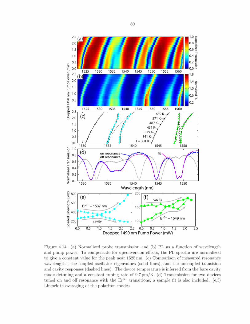
80
1525 1530 1535 1540 1545 1550 1555 15600.0
0.5
1.0
1.5
2.0
2.5
0.2
0.4
0.6
0.8
1.0
Dro
pp
ed
14
90
nm
Pu
mp
Po
we
r (m
W)
0.0
0.5
1.0
1.5
2.0
2.5
0.2
0.6
1.0
1.4
1.8
1525 1530 1535 1540 1545 1550 1555 1560
No
rma
lized
Tra
nsm
ission
No
rma
lized
PL
(a)
(b)
No
rma
lize
d T
ran
smis
sio
n
Wavelength (nm)
0.2
0.4
0.6
0.8
1.0
0.01530 1535 1540 1545 1550
(d) on resonanceoff resonance
fit
200
400
600
800
Lo
ad
ed
Lin
ew
idth
(G
Hz)
100
150
200
0.0 0.5 1.0 1.5 2.0 2.5 0.0 0.5 1.0 1.5 2.0 2.5
Dropped 1490 nm Pump Power (mW)
(e) (f )
Er3+ – 1537 nm
Er3+ – 1549 nmcavity
cavity
1530 1535 1540 1545 15500.0
0.5
1.0
1.5
2.0
2.5
(c)
T = 301 K
341 K
379 K
431 K
487 K
571 K
639 K
Figure 4.14: (a) Normalized probe transmission and (b) PL as a function of wavelengthand pump power. To compensate for upconversion effects, the PL spectra are normalizedto give a constant value for the peak near 1525 nm. (c) Comparison of measured resonancewavelengths, the coupled-oscillator eigenvalues (solid lines), and the uncoupled transitionand cavity responses (dashed lines). The device temperature is inferred from the bare cavitymode detuning and a constant tuning rate of 9.7 pm/K. (d) Transmission for two devicestuned on and off resonance with the Er3+ transitions; a sample fit is also included. (e,f)Linewidth averaging of the polariton modes.
81
Table 4.3: Summary of cavity-polariton parameters at T > 300 K
Polariton γinh/2π δωvrs/2π ∆ω/2π ∆ω data γh/2π |gN |/2π(GHz) (GHz) (GHz) source (GHz) (GHz)
1537.2 nm
130 198435.8510
Absorption
Luminescence
361475
113128
1549.2 nm
59 11494.3135
Absorption
Luminescence
57115
3139
measured high-temperature linewidths (∆ω). We use the γinh values for Y1↔Z1 and Y ′1↔Z ′
1
in Table 4.2 which assumed γh/2π = 10 GHz at 8.6 K; errors in γinh due to this assumption
(error < 6GHz) are less significant at 300 K because the total linewidths are larger. Greater
uncertainty arises if nearly resonant transitions between other Stark levels further inhomo-
geneously broaden the absorption lines. For simplicity, we assume this increase is marginal
compared to γh. Finally, the measured values for ∆ω differ in the absorption spectrum
[obtained from Fig. 4.14(e,f) when the WGMs are not resonant] and in the PL spectrum
[from the full width at half maximumin Fig. 4.5(a)]. The results for δωvrs,∆ω, γh are
summarized in Table 4.3 along with the calculated gN values for each transition.12 For
comparison, the Rabi splitting for a homogeneously broadened atomic ensemble is
δωvrs = 2
√
|gN |2 − 1
4
(
κ− γh
2
)2, (4.18)
where κ is the cavity field decay rate in the absence of the atomic transition [214]. Neglecting
the inhomogeneous broadening, the fitted splitting around 1537.2 nm and Eq. (4.18) give
|gN |/2π = 105 GHz with δωvrs, κ, γh/2π = 198, 113, 361 GHz. Given that γinh can also
slightly reduce the observed splitting, the method in the previous section predicts 113 GHz
with the absorption spectrum linewidth (which is preferred in Ref. [222]). Following the
generally observed behavior for the magnetic-dipole transitions on the C3i sites, the Rabi
splitting around Y ′1↔Z ′
1 at 1549.2 nm is larger than expected from the absorption. Treating
this polariton resonance as a single homogeneous transition shows δωvrs ≈ 2|gN | and γh is
not significant—in Eq. (4.18), |gN |/2π = 58 GHz with δωvrs, κ, γh/2π = 114, 50, 57 GHz.
We are also working to understand why high-temperature polaritons only form around
Y1↔Z1 transitions and not around transitions involving higher Stark levels with similar
12The inhomogenous linewidths obtained at T = 8K are repeated for completeness.
82
absorption peaks.
The robust collective coupling we have observed between Er3+ transitions and the optical
modes in Er2O3 resonators is an appealing route to improving the material’s efficiency
or gain through cQED effects, like cavity-enhanced superradiance [235] and the Purcell
Effect [4]. Unfortunately to achieve superradiant emission, with yield increasing as N2,
the ensemble must be first excited into a Dicke state that quickly decoheres due to fast
dephasing above cryogenic temperatures and excitation diffusion [236]. Because collective
relaxation of the polariton modes is difficult to initiate, Purcell enhanced emission from
individual Er3+ ions is a more promising direction and can be realized by decreasing Veff
to increase the coupling rate per ion [6, 214]. From the perspective of a single excited ion
in the present devices, the other (N–1) ions create a dispersive resonance in the refractive
index that generates the paired polariton modes [213]. The weak coupling between each ion
and the large WGM at rate g1 can then be treated perturbatively, which causes negligible
enhanced for these system parameters—the expected Purcell “enhanced” lifetime κ/2g21 >
150 ms [214] is much longer than the 7.2 µs (8 ms) bulk nonradiative (radiative) lifetime.
Quantum master equation models produce similar behaviour using a single Er3+ ion and a
“privileged” ion coupled to an optical cavity mode at rates of g1 and gN , respectively. By
integrating proposed ultrasmall mode volumes formed using nanoscale slots [18] with recent
low-loss photonic crystals in Si [237], a hybrid Si cavity containing a Er2O3 slot [∆n ≈ 1.5,
Veff ≈ 0.18(λ/n)3, Q ≈ 106, κ/2π ≈ 100 MHz] could exhibit an enhanced emission lifetime
of κ/2g21 ≈ 0.23 µs.
4.2.6 Rate Equation Estimates
In more conventional cavities where the Purcell Effect is negligible, the large Er2O3 upcon-
version rate at low pump power alters the population dynamics for the Er3+ levels when
compared to the quasi-two-level system present in fiber amplifiers [165]. To accurately de-
scribe an Er2O3 cavity at the pump rates used during the radiative efficiency measurement
(Fig. 4.9), a rate equation model must include the populations of several excited states
(likely all levels up through 4S3/2 and 2H11/2) and the accompanying coupling terms and
coefficients (e.g., radiative and nonradiative decay into other levels or upconversion paths).
However with only the τrad, τnr, Cup parameters for 4I13/2, we can roughly estimate the
power necessary to reach transparency in the C/L-bands by solving a simplified three-state
83
model for pumping at ∼1480 nm:
N1 = NEr −N2 −N3, (4.19)
dN2
dt= −N2
τnr− CupN
22 + sΦ(N1 − rN2), (4.20)
dN3
dt= −N3
τnr+
1
2CupN
22 . (4.21)
The populations N1,N2,N3 represent densities for ions in the 4I15/2,4I13/2,
4I9/2 states,
respectively; higher states are neglected because we lack reasonable estimates for the appro-
priate upconversion and/or excited-state absorption coefficients. The 4I11/2 level is omitted
because it quickly decays to 4I13/2 through multiphonon emission—this assumption pro-
duces a lower effective upconversion rate into 4I9/2. For simplicity, the crystal-field splitting
for all levels is ignored except that the emitted photons from 4I13/2 are red-shifted from
pump photons. The total ion density on C2 lattice sites (NEr) is 2.05×1022 cm−3, and we use
our estimated value for the cooperative upconversion coefficient Cup = 5.1×10⁻¹⁶ cm−3/s.
We assume the 4I13/2 and 4I9/2 lifetimes are approximately equal (τnr = 7.2µs) because
both transitions to the ground state are dipole forbidden and likely subject to similar exci-
tation diffusion rates. This analysis excludes spontaneous emission (low radiative efficiency)
and stimulated emission (leaky cavity at the emission wavelength). The pump photon flux
within the cavity is given by Φ, and r is the ratio of the emission and absorption cross sec-
tions at the pump wavelength. For Er3+-doped silica, r ≈ 1/3 at 1480 nm [165] and accounts
for emission stimulated by the pump beam. The adjustable parameter s = 2.5×10⁻¹² en-
compasses a number of factors including the value of the absorption cross section; it is set to
give N2 ≈ 2.7×1020 cm−3 at Pd = 204 µW—corresponding to the inferred values from the
radiative efficiency results in Fig. 4.9. This model for the Er3+ transitions is then applied
to a microdisk cavity (20 µm radius, material volume V = ΓVeff = 20.1 µm3).
Steady-state solutions to these rate equations give approximate pump powers at which
N2 ≈ N3 and at which these transitions near transparency. By Pd ≈ 0.6 mW, there are
∼5×10²⁰ ions/cm3 in both the 4I13/2 and 4I9/2 levels. These microdisks approach trans-
parency for 4I9/2→4I15/2 (λ ≈ 800 nm) and 4I13/2→4I15/2 (λ ≈ 1480 nm) with pump powers
of Pd ≈ 18 mW and Pd ≈ 130 mW, respectively. To improve the accuracy, this model should
include 4S3/2, which would encompass the minimum number of levels to account for the
green emission. Since the upconverted luminescence is most intense around λ ≈ 550 nm,
84
the combined upconversion-emission path for 4I9/2→4S3/2→4I15/2 may provide a fast route
back to the ground state. A fast green relaxation would increase the transparency thresholds
and may make the 4I9/2→4I15/2 relaxation a secondary process. Exploratory pulsed mea-
surements using a Tm3+-doped fiber amplifier at 1480 nm also suggest some of the upper
levels may be longer lived (on the order of 100µs). In summary, the upconversion processes
close to transparency are quick enough to produce substantial populations in every level up
to and including 4S3/2, and the 4I13/2 level is likely not the first level to reach transparency
when pumping at ∼1480 nm.
4.3 Conclusions
The rate-equation estimates suggest a prohibitive amount of power is required to invert
the 4I15/2 manifold in microphotonic Er2O3 cavities due to the fast excitation diffusion
to nonradiative sites and the large cooperative upconversion coefficient. Since the rapid
upconversion prevents transparency in the C-band until most of the ions are sequestered
in higher states, individual upper levels (e.g., 4S3/2) may be the first to invert relative to
the ground state making Er2O3 upconversion green lasers a possibility [187–190]. Epitaxial
Er2O3-on-Si might also be developed into an incoherent visible emitter—rough estimates
based on the camera’s sensitivity in Fig. 4.9 give a green radiative efficiency on the order
of 5% for an absorbed power density of 0.15 mW/µm3. Additionally, there is potential for
using Er2O3 to shift infrared radiation into the visible spectrum (i.e., above the bandgap of
silicon) as part of multijunction silicon solar cells.
To achieve technological maturity for the original application of Er2O3 to waveguide
amplifiers and lasers for on-chip optical networks, it is possible, but improbable, that the
performance of pure Er2O3 films can be improved by identifying and eliminating the quench-
ing impurities and finding suitable dopants to screen the ion-ion interactions. More likely,
future progress will be due to the precision and flexibility of the ALE growth. Ternary
oxides with Y and Gd, such as (Y1−xErx)2O3, would be better lattice matched to silicon,
and their lack of infrared and visible transitions would slow the upconversion and non-
radiative processes by increasing the inter-ion separation for the optically active species.
Detailed relaxation studies (as in Ref. [202]) of these alloys are necessary to characterize
the excitation diffusion and to optimize the emitter density for the desired gain. Electrolu-
85
minescence may be achieved through R2O3-Si heterostructures and superlattices [238–240],
but efficient excitation must be explored first including the alignment of the R2O3 4f levels
to the Si bands. Finally, the spectral response of rare-earth oxides can be designed for spe-
cific applications. For example, (Gd1−xPrx)2O3 may be more suitable for silicon photonics
because the 1G4→3H5 transition in Pr3+ at 1310 nm does not terminate in the ground state
(3H4) and operates at the same wavelength as SiGe electro-absorption modulators [156] and
APDs [241], and the phase space for engineering sensitization and cross-relaxation processes
increases significantly in quaternary oxides. As in III-V systems, high-quality epitaxy will
become crucial in controlling the material’s structure and optical properties while moving
toward CMOS-compatible rare-earth laser diodes and photodetectors.
86
Appendix A
Experimental Supplement
A.1 Mach-Zehnder Interferometer
The accurate determination of spectral linewidths is essential to much of this research. The
typical testing arrangement in Fig. 2.4 employs an external-cavity tunable diode laser to
sweep across the desired wavelengths and a computer to synchronize the laser’s reference
output (or start trigger) with the analog transmission/reflection signal acquired by the
photodetector. The method and accuracy of this synchronization depends on the laser
model and is particular to each unit. For example, the piezo-tuning mode for the New
Focus Velocity lasers applies a sawtooth waveform to a piezoelectric element attached to
the tuning mirror; the computer also receives this waveform and applies a set calibration to
its amplitude to determine the wavelength. Unfortunately, the wavelength span can vary
up to 10% from day to day for a given voltage, and the forward and backward scans are
hysteretic (see Ref. [60] for more information). Another common problem in older Velocity
lasers is that the position sensor on their tuning arm (used for coarse motor scans) can
begin to malfunction and produce an offset between the laser’s true wavelength and the
wavelength indicated by the laser head—this offset can be removed during post-processing
using the OSA. In general, the repeatability issues with the Velocity lasers do not impede
daily testing, but precise measurements over several days (e.g., Ref. [56]) require calibration.
In contrast, the discontinued Vidia lasers only send a single pulse at the beginning of the scan
(after their acceleration phase), and the computer simply assumes the laser is sweeping at
the set rate after that time. To date, there has been no need to repeatedly calibrate narrow
Vidia sweeps.
To calibrate a laser’s sweep range, we use a fiber-based Mach-Zehnder interferome-
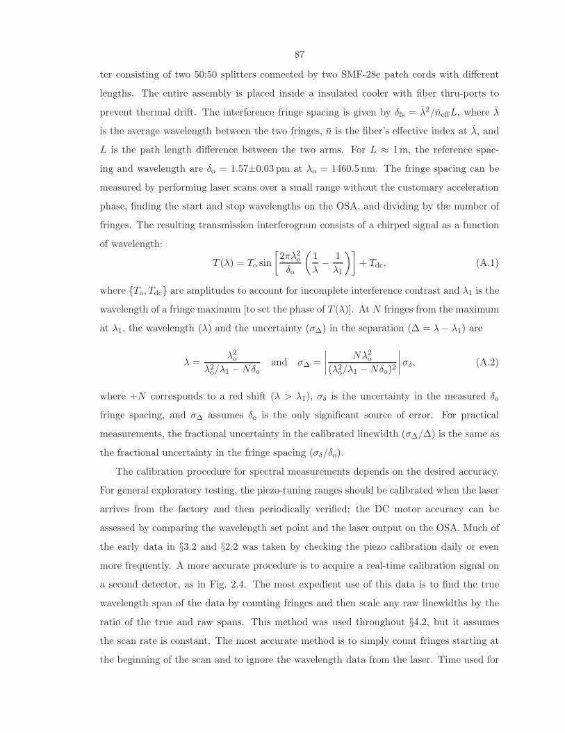
87
ter consisting of two 50:50 splitters connected by two SMF-28e patch cords with different
lengths. The entire assembly is placed inside a insulated cooler with fiber thru-ports to
prevent thermal drift. The interference fringe spacing is given by δfs = λ2/neffL, where λ
is the average wavelength between the two fringes, n is the fiber’s effective index at λ, and
L is the path length difference between the two arms. For L ≈ 1m, the reference spac-
ing and wavelength are δo = 1.57±0.03 pm at λo = 1460.5 nm. The fringe spacing can be
measured by performing laser scans over a small range without the customary acceleration
phase, finding the start and stop wavelengths on the OSA, and dividing by the number of
fringes. The resulting transmission interferogram consists of a chirped signal as a function
of wavelength:
T (λ) = To sin
[
2πλ2o
δo
(
1
λ− 1
λ1
)]
+ Tdc, (A.1)
where To, Tdc are amplitudes to account for incomplete interference contrast and λ1 is the
wavelength of a fringe maximum [to set the phase of T (λ)]. At N fringes from the maximum
at λ1, the wavelength (λ) and the uncertainty (σ∆) in the separation (∆ = λ− λ1) are
λ =λ2
o
λ2o/λ1 −Nδo
and σ∆ =
∣
∣
∣
∣
Nλ2o
(λ2o/λ1 −Nδo)2
∣
∣
∣
∣
σδ, (A.2)
where +N corresponds to a red shift (λ > λ1), σδ is the uncertainty in the measured δo
fringe spacing, and σ∆ assumes δo is the only significant source of error. For practical
measurements, the fractional uncertainty in the calibrated linewidth (σ∆/∆) is the same as
the fractional uncertainty in the fringe spacing (σδ/δo).
The calibration procedure for spectral measurements depends on the desired accuracy.
For general exploratory testing, the piezo-tuning ranges should be calibrated when the laser
arrives from the factory and then periodically verified; the DC motor accuracy can be
assessed by comparing the wavelength set point and the laser output on the OSA. Much of
the early data in §3.2 and §2.2 was taken by checking the piezo calibration daily or even
more frequently. A more accurate procedure is to acquire a real-time calibration signal on
a second detector, as in Fig. 2.4. The most expedient use of this data is to find the true
wavelength span of the data by counting fringes and then scale any raw linewidths by the
ratio of the true and raw spans. This method was used throughout §4.2, but it assumes
the scan rate is constant. The most accurate method is to simply count fringes starting at
the beginning of the scan and to ignore the wavelength data from the laser. Time used for
88
further improvements would likely be better spent building another MZI with smaller δo
and σδ.
The pure fringe counting method has been implemented to calibrate large wavelength
ranges while studying dispersion-engineered microdisks for degenerate four-wave mixing.
Designed and fabricated by Q. Lin, the disks consist of a Si core and SiO2 cladding to
control the GVD, similar to the waveguides in Ref. [117]. The disks are repeated oxidized
to tune the ZDWL for the TMp=1 modes toward 1550 nm in order to achieve momentum
and energy conservation for four-wave mixing between three consecutive modes. Because
future experiments call for a coarse wavelength division multiplexer (20 nm channel spac-
ing), the FSRs separating the signal and idler modes from the pump mode must be ap-
proximately equal to the channel spacing (2530 GHz) with mismatched comparable to the
modes’ linewidths (∼0.6 GHz). For comparing two wavelength spans, the measurement is
less sensitive to uncertainty in δo, and the uncertainty in the difference (∆1 −∆2) between
the two spans is
σ(∆1 − ∆2) =
∣
∣
∣
∣
N1λ2o
(λ2o/λ1 − δoN1)2
− N2λ2o
(λ2o/λ2 − δoN2)2
∣
∣
∣
∣
σδ. (A.3)
Using the MZI and sampling every ∼0.1 pm, Fig. A.1 shows a sample calibrated data set
for a device with signal and idler modes well matched about the pump mode at 1528.8 nm.
The difference between the calibrated and raw wavelengths is at most 0.25 nm, and the scan
rate is clearly not linear. The pump-signal and pump-idler separation is ∼2676.7 GHz with
a difference of 0.2±2.8 GHz, which is a relative error of 0.1%. To achieve the necessary ac-
curacy of .0.02%, the MZI fringe spacing must be increased to δo ≈ 7 pm if the uncertainty
in the spacing cannot be reduced (σδ = ±0.03 pm).
In the current implementation, the MZI reference signal is loaded into an (N×1) matrix
and analyzed as a function of the matrix index. First, the mean is subtracted, and a zero-
finding routine determines the “fractional” indices where the fringes cross the axis. These
positions in the matrix are separated in wavelength by half the fringe spacing, and they pro-
vide a piecewise function for interpolating the indices of the original vector onto calibrated
wavelengths. Since the reference and transmission signals are sampled simultaneously, the
same calibrated wavelength vector applies to the transmission data. The dependence of the
fringe spacing on wavelength is included by quadratically scaling δfs at each “zero” crossing
89
1510 1520 1530 1540 1550 1560 1570
0.0
0.2
0.4
0.6
0.8
1.0
1.2
1.4
1.6
1.8
2.0
Wavelength (nm)
Dete
cto
r S
ignal (V
)
Δλ = 10 pm
−0.05
0.00
0.05
0.10
0.15
0.20
0.25
1510 1520 1530 1540 1550 1560 1570
Wavelength (nm)
λcalib
- λ
data
(nm
)
(a)
(b)
2676.80 GHz 2676.60 GHz 2678.06 GHz
TM trans.
TE trans.
MZI ref.
Figure A.1: (a) Raw TE- and TM-polarized transmission spectra for a Si-SiO2 microdiskafter calibrating the wavelength. The MZI reference signal was acquired concurrently withthe TM spectrum. Nearly equal FSRs between the highlighted TMp=1 modes shows theZDWL is near 1530 nm. The inset contains a 10-pm section of the calibration signal showingmeasured data points (∗) and the interpolated “zero” crossings (). (b) Difference betweenthe calibrated and raw wavelengths for a long Vidia laser scan.
90
to δ′fs = δo(λ′/λo)
2 where the reference splitting again is δo = 1.57 pm at λo = 1460.5 nm.
It assumes the starting wavelength is accurate; the lasers’ ±0.05 nm repeatability is suffi-
cient for these purposes. This method also ignores dispersion in the optical fiber because
it introduces a correction an order of magnitude smaller than the present uncertainty in
δfs,o. For completeness, the dispersion can be calculated using parameters obtained from the
manufacturer (Corning for SMF-28e) and is presented below for 1200 nm ≤ λ ≤ 1625 nm:
D ≡ −2πc
λ2
(
∂2k
∂ω2
)
=πcSo
2
[
1
ω− ω3
ω4o
]
, (A.4a)
ng = π2c3So
[
ω2
2ω2o
+1
2ω2
]
+ C1, (A.4b)
neff = π2c3So
[
ω2
6ω4o
− 1
2ω2
]
+ C1 +C2
ω, (A.4c)
where ωo/2π = 228.3 THz (λo = 1313 nm) is the zero-dispersion frequency, the slope of
D(ω = ωo) is So = 0.086 ps/(nm2·km), C1 = 1.45647 is an integration constant to give
ng = 1.4682 at 1550 nm and 1.4676 at 1310 nm (specified by Corning), and the second
integration constant C2 = −4.6547×10¹² rad/s gives neff = 1.4462 at 1550 nm (via FEM
using 0.36% core-cladding contrast, a core diameter of 8.2 µm, and a cladding index of
refraction for pure silica n = 1.4440). With the correction to neff , the fringe spacing
at 1568 nm is 1.8128 pm, and it decreases by less than 2 fm when dispersion is neglected
(δfs = 1.8109 pm). The (λ′/λo)2 scaling has been verified to within the accuracy of the
measurements for wavelengths from 1460 to 1625 nm.
A.2 Pulse Optimization for EOSPACE Modulators
The performance specifications for the LiNbO3 electro-optic modulators from EOSPACE
are typically given for general use when the modulator is biased to give a linear response to
the signal voltage. Because many factors contribute the EOM’s operation, only a minimum
extinction ratio is specified, but this value can be exceeded by 15 dB or more by carefully
controlling the bias and polarization. To achieve square pulses with minimum insertion loss
and &35 dB extinction using the standard 10 Gb/s modulator (nominal extinction ratio of
>20 dB),

91
1) Connect the laser source and a FPC1 to the modulator, and affix the modulator
and patch cords to the optical table. Maximizing the extinction ratio requires great
stability in the polarization and source wavelength. Let the laser warm up and adjust
any fiber and electrical connections prior to this procedure.
2) Attach the modulator’s output pigtail to the table. The output does not need to be
stabilized to the same extent as the input, but movement of the output fiber should
not cause the modulator’s input to shift.
3) With the output connected to an OSA or power meter, maximize the transmission
polarization and modulator’s DC bias to calibrate the modulator’s insertion loss. This
step needs to be done only once.
4) Optimize the polarization and DC bias to minimize the transmission. The optimal
polarization should be close to that found in the previous step.
5) Wait. The modulator takes a few hours to fully settle. Periodically readjust the
polarization (should not significantly change) and DC bias to minimize transmission.
The bias must be monitored frequently at first while the transmission is changing
rapidly. At >30 dB extinction, the transmission will be very sensitive to any small
changes.
6) Once the EOM has settled, it requires small tweaks to maintain the maximum extinc-
tion.
7) Connect the EOM output to an oscilloscope. Be aware of the maximum peak power
for the high-speed detectors, and attenuate the optical pulses if needed.
8) Set the amplitude of the RF signal/pulses to obtain the desired optical waveform
and measure the peak power. Prior to acquiring data, it is prudent to examine the
optical signal produced by the modulator and a given voltage source. For example,
the trailing edge of pulses from the Avtech pulse generator (AVPP–1–C) overshoots
zero and produces a small secondary pulse. These after pulses are ∼15 dB attenuated
from the main pulse and occur ∼15 ns after the trailing edge; the exact waveform is
1The FPC may not be necessary when using polarization-maintaining (PM) fiber, but this procedureassumes the polarization of a standard single-mode fiber must be matched to the modulator’s PM inputfiber.
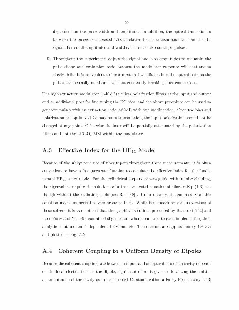
92
dependent on the pulse width and amplitude. In addition, the optical transmission
between the pulses is increased 1.2 dB relative to the transmission without the RF
signal. For small amplitudes and widths, there are also small prepulses.
9) Throughout the experiment, adjust the signal and bias amplitudes to maintain the
pulse shape and extinction ratio because the modulator response will continue to
slowly drift. It is convenient to incorporate a few splitters into the optical path so the
pulses can be easily monitored without constantly breaking fiber connections.
The high extinction modulator (>40 dB) utilizes polarization filters at the input and output
and an additional port for fine tuning the DC bias, and the above procedure can be used to
generate pulses with an extinction ratio >62 dB with one modification. Once the bias and
polarization are optimized for maximum transmission, the input polarization should not be
changed at any point. Otherwise the laser will be partially attenuated by the polarization
filters and not the LiNbO3 MZI within the modulator.
A.3 Effective Index for the HE11 Mode
Because of the ubiquitous use of fiber-tapers throughout these measurements, it is often
convenient to have a fast ,accurate function to calculate the effective index for the funda-
mental HE11 taper mode. For the cylindrical step-index waveguide with infinite cladding,
the eigenvalues require the solutions of a transcendental equation similar to Eq. (1.6), al-
though without the radiating fields (see Ref. [49]). Unfortunately, the complexity of this
equation makes numerical solvers prone to bugs. While benchmarking various versions of
these solvers, it is was noticed that the graphical solutions presented by Barnoski [242] and
later Yariv and Yeh [49] contained slight errors when compared to code implementing their
analytic solutions and independent FEM models. These errors are approximately 1%–3%
and plotted in Fig. A.2.
A.4 Coherent Coupling to a Uniform Density of Dipoles
Because the coherent coupling rate between a dipole and an optical mode in a cavity depends
on the local electric field at the dipole, significant effort is given to localizing the emitter
at an antinode of the cavity as in laser-cooled Cs atoms within a Fabry-Perot cavity [243]
93
0 1 2 3 4 5 6 7
1.0
1.1
1.2
1.3
1.4
1.5
neff
for HE11 modes...
Barnoski (1976) Fig. A.4
Yariv and Yeh (2007) Fig. B.6
Analytic solver
FEM results
V = R(n1-n2)1/222
single mode cut off:
λo = 1550 nm, R = 0.56 μm
2λo
Figure A.2: Comparison of neff values for the HE11 mode of a fiber-taper or step-indexoptical fiber with n1 = 1.45 (silica) and n2 = 1.0 (air). Data points for the published curvesby Barnoski [242] and Yariv and Yeh [49] were scanned and digitally extracted from theoriginal sources. The analytic solver was implemented by P. Barclay. The FEM modelcalculated neff at a fixed wavelength (1550 nm) while varying the core radius from 0.2 to1.5µm.
and precisely aligning photonic crystal cavities to buried quantum dots [244]. For many-
body systems, the collective interaction must account for the field seen at every dipole.
Cooperative interactions delocalize the excitations in Er2O3 and highly doped solids, and
the dipoles can be treated approximately as a gas. Following Ref. [219], the collective
coupling rate (gN ) is proportional to the mean rate experienced by each dipole (g1):
|gN |2 = N |g1|2 =
∫
ρ(~r)|g1(~r)|2dV, (A.5)
where ρ(~r) and N are the distribution and number of dipoles, respectively. The coupling
rate for a single emitter within the cavity mode is
g1(~r) =
√
|~µ|2ωc
2ℏǫ(~r)VeffU(~r), (A.6)
where U(~r) describes the cavity field and is normalized so∫
|U(~r)|2dV = Veff [6]. If the
dipole density (ρo) within the solid is uniform, Eq. (A.5) simplifies to
gN =|~µ|2ωcρo
2ℏn2ǫoVeff
∫
δV|U(~r)|2dV, (A.7)
94
where n is the refractive index of the dipole medium. The integral is taken over the vol-
ume containing the dipoles (δV ) where ρ(~r) 6= 0. By inspecting Eqs. (1.28) and (1.29),∫
δV|U(~r)|2dV = ΓVeff , and the collective coupling rate is independent of the cavity size,
|gN |2 = N |g1|2 ≈ |~µ|2ωcρΓ
2ℏn2ǫ0, (A.8)
which is consistent with the classical approach of treating many-atom Rabi splitting as a
consequence of absorption [213].
95
Appendix B
Calculation of the β-Factor for
Er2O3 Microdisks
In laser physics, the β-factor is the ratio near the lasing threshold of the spontaneous
emission into the lasing mode over the emission into all modes, and it can range from 10−6
to 10−5 for large gas lasers to nearly 100 for few quantum-dot microcavity lasers [245]. In
this work, we modify this definition so β is the ratio of emitted power into a chosen subset of
modes (P ′c,T ) over the total power emitted into free-space (Pfs,T ) and cavity modes (Pc,T ):
β =P ′
c,T
Pfs,T + Pc,T. (B.1)
From Fermi’s Golden rule, the total emitted power (PT ) in a given spectral range is approx-
imately
PT =2π
ℏ
∫
ρf
∣
∣〈ψf |Hint|ψi〉∣
∣
2NErℏωidωi, (B.2)
where ρf is the density of final states andNEr is the number of excited Er3+ ions. We express
the final density of states as a product of the density of electronic states (ρe) per energy
per ion and the density of emission modes (ρm) per unit frequency. Using a semiclassical
electric-dipole interaction Hint = −q ~E · ~r and averaging over all polarizations and wave
vectors for a fixed dipole orientation, PT can be expressed as
PT =2π
3ℏ
∫
ρf
∣
∣〈 ~E(ωi)〉∣
∣
2∣∣~µ(ωi)
∣
∣
2NErℏωidωi, (B.3)
where 〈 ~E(ωi)〉 is the time-averaged electric-field strength per emitted photon and the
|ψi〉→|ψf 〉 transition’s dipole moment is ~µ(ωi) = −q〈ψf |~x|ψi〉. For emission into free-space
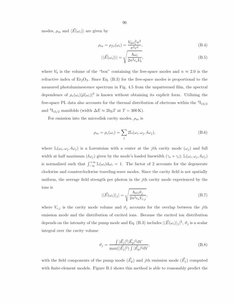
96
modes, ρm and 〈 ~E(ωi)〉 are given by
ρm = ρfs(ωi) =Vbω
2i n
3
π2c3, (B.4)
|〈 ~E(ωi)〉| =
√
ℏωi
2n2ǫoVb, (B.5)
where Vb is the volume of the “box” containing the free-space modes and n ≈ 2.0 is the
refractive index of Er2O3. Since Eq. (B.3) for the free-space modes is proportional to the
measured photoluminescence spectrum in Fig. 4.5 from the unpatterned film, the spectral
dependence of ρe(ωi)|~µ(ωi)|2 is known without obtaining its explicit form. Utilizing the
free-space PL data also accounts for the thermal distribution of electrons within the 4I13/2
and 4I15/2 manifolds (width ∆E ≈ 2kBT at T = 300 K).
For emission into the microdisk cavity modes, ρm is
ρm = ρc(ωi) =∑
j
2L(ωi, ωj , δωj), (B.6)
where L(ωi, ωj, δωj) is a Lorentzian with a center at the jth cavity mode (ωj) and full
width at half maximum (δωj) given by the mode’s loaded linewidth (γe + γi); L(ωi, ωj, δωj)
is normalized such that∫ +∞
−∞L(ωi)dωi = 1. The factor of 2 accounts for the degenerate
clockwise and counterclockwise traveling-wave modes. Since the cavity field is not spatially
uniform, the average field strength per photon in the jth cavity mode experienced by the
ions is
|〈 ~E(ωi)〉j | =
√
ℏωiϑj
2n2ǫoVc,j, (B.7)
where Vc,j is the cavity mode volume and ϑj accounts for the overlap between the jth
emission mode and the distribution of excited ions. Because the excited ion distribution
depends on the intensity of the pump mode and Eq. (B.3) includes |〈 ~E(ωi)〉j |2, ϑj is a scalar
integral over the cavity volume
ϑj =
∫
| ~Ej |2| ~Ep|2dVmax(| ~Ej |2)
∫
| ~Ep|2dV, (B.8)
with the field components of the pump mode ( ~Ep) and jth emission mode ( ~Ej) computed
with finite-element models. Figure B.1 shows this method is able to reasonably predict the
97
Measured
Theory (p = 1)
Theory (p = 2)
PL Spectrum
Colle
cte
d P
L (p
W)
1520 1540 1560 1580 1600 1620 1640 1660 1680 1700
1.0
Wavelength (nm)
0.8
0.6
0.4
0.2
0.0 0
40
80
120
160
200
Pc,j
max(Pc,j)
Figure B.1: Comparison of calculated and measured spontaneous emission into Er2O3
WGMs. The PL intensity is calculated using Eqs. (B.3,6–8), and the measured powerinto each mode is integrated and corrected for collection losses according to Eq. (4.5). Sincethe exact values for ρe(ωi)|~µ(ωi)|2 and the absolute collection efficiency are unknown, thetheoretical and empirical values for Pc,j are normalized to their maxima—i.e., this graphcompares the PL intensity in each mode relative to modes near the emission peak. The PLspectrum was excited by pumping a TEp=1 mode at 1493.3 nm [repeated from Fig. 4.9(b)];the TEp=1 emission modes are again highlighted in gray. Beyond our lasers’ ranges, thefractional PL in the observed peaks at λ > 1620 nm is overestimated because the WGMsare extremely over coupled and we can only approximate γi, γe.
fractional emission into each WGM.
Using the thin film PL data and the cavity mode parameters, the β-factor can be calcu-
lated for any individual or collection of modes. While Pc,T in Eq. (B.1) includes a summation
over all cavity modes (both observed and unobserved1), the ϑj/Vc,j factor heavily weights
the contribution of the modes with low radial order. In this analysis we include the quasi-TE
modes of the first 8 radial families; the quasi-TM modes are poorly confined and have little
overlap with the Er3+ ions. For first and second radial-order emission modes at λ > 1520 nm
as in the radiative efficiency measurement, we estimate βobs = 0.091 which is in reasonable
agreement with the experimental value of 0.038. Increasing the sum to include all observed
modes across the S/C/L-bands (Fig. 4.4) gives β12 = 0.127. By including all the cavity
modes in P ′c,T , βT = 0.227 is the fraction of the total 4I13/2→4I15/2 photoluminescence that
is emitted into the microdisk WGMs.
1The higher-order quasi-TE modes have large bending losses (Q < 100) and are poorly phase matchedto the taper waveguide. Since they cannot be observed in transmission or taper-collected PL, all necessaryparameters are obtained through finite-element simulations.

98
Bibliography
[1] R. K. Chang and A. J. Campillo, eds., Optical Processes in Microcavities (World Scientific,
Singapore, 1996).
[2] K. Vahala, ed., Optical Microcavities (World Scientific, Singapore, 2004).
[3] Y. Yamamoto and R. E. Slusher, “Optical Processes in Microcavities,” Phys. Today 46(6),
66–73 (1993).
[4] E. M. Purcell, “Spontaneous emission probabilities at radio frequencies,” Phys. Rev. 69, 681
(1946).
[5] S. Haroche and D. Kleppner, “Cavity Quantum Electrodynamics,” Phys. Today 42(1), 24–30
(1989).
[6] H. J. Kimble, “Strong interactions of single atoms and photons in cavity QED,” Physica
Scripta T76, 127–137 (1998).
[7] J. Bravo-Abad, A. Rodriguez, P. Bermel, S. G. Johnson, J. D. Joannopoulos, and M. Soljacic,
“Enhanced nonlinear optics in photonic-crystal microcavities,” Opt. Express 15(24), 16161–
16176 (2007).
[8] M. Notomi, T. Tanabe, A. Shinya, E. Kuramochi, H. Taniyama, S. Mitsugi, and M. Morita,
“Nonlinear and adiabatic control of high-Qphotonic crystal nanocavities,” Opt. Express
15(26), 17458–17481 (2007).
[9] R. W. Boyd and J. E. Heebner, “Sensitive Disk Resonator Photonic Biosensor,” Appl. Opt.
40(31), 5742–5747 (2001).
[10] T. J. Kippenberg and K. J. Vahala, “Cavity Opto-Mechanics,” Opt. Express 15(25), 17172–
17205 (2007).
[11] C. Weisbuch, M. Nishioka, A. Ishikawa, and Y. Arakawa, “Observation of the coupled exciton-
photon mode splitting in a semiconductor quantum microcavity,” Phys. Rev. Lett. 69(23),
3314–3317 (1992).
99
[12] P. Kelkar, V. Kozlov, H. Jeon, A. V. Nurmikko, C.-C. Chu, D. C. Grillo, J. Han, C. G. Hua,
and R. L. Gunshor, “Excitons in a II-VI semiconductor microcavity in the strong-coupling
regime,” Phys. Rev. B 52(8), R5491–R5494 (1995).
[13] D. G. Lidzey, D. D. C. Bradley, T. Virgili, A. Armitage, M. S. Skolnick, and S. Walker,
“Room Temperature Polariton Emission from Strongly Coupled Organic Semiconductor Mi-
crocavities,” Phys. Rev. Lett. 82(16), 3316–3319 (1999).
[14] M. Pelton, C. Santori, J. Vucovic, B. Zhang, G. S. Solomon, J. Plant, and Y. Yamamoto,
“Efficient source of single photons: A single quantum dot in a micropost microcavity,” Phys.
Rev. Lett. 89, 233602 (2002).
[15] E. Yablonovitch, “Inhibited Spontaneous Emission in Solid-State Physics and Electronics,”
Phys. Rev. Lett. 58(20), 2059–2062 (1987).
[16] J. D. Joannopoulos, S. G. Johnson, J. N. Winn, and R. D. Meade, Photonic Crystals: Molding
the Flow of Light, 2nd ed. (Princeton University Press, Princeton, 2008).
[17] B.-S. Song, S. Noda, T. Asano, and Y. Akahane, “Ultra-high-Q photonic double-
heterostructure nanocavity,” Nature Mater. 4, 207–210 (2005).
[18] J. T. Robinson, C. Manolatou, L. Chen, and M. Lipson, “Ultrasmall Mode Volumes in Dielec-
tric Optical Microcavities,” Phys. Rev. Lett. 95(14), 143901 (2005).
[19] C. G. B. Garrett, W. Kaiser, and W. L. Bond, “Stimulated Emission into Optical Whispering
Modes of Spheres,” Phys. Rev. 124(6), 1807–1809 (1961).
[20] S. L. McCall, A. F. J. Levi, R. E. Slusher, S. J. Pearton, and R. A. Logan, “Whispering-gallery
mode microdisk lasers,” Appl. Phys. Lett. 60, 289–291 (1992).
[21] D. K. Armani, T. J. Kippenberg, S. M. Spillane, and K. J. Vahala, “Ultra-high-Q toroid
microcavity on a chip,” Nature 421, 925–928 (2003).
[22] K. Srinivasan and O. Painter, “Momentum space design of high-Q photonic crystal optical
cavities,” Opt. Express 10(15), 670–684 (2002).
[23] D. Englund and J. Vuckovic, “A direct analysis of photonic nanostructures,” Opt. Express 14,
3472–3483 (2006).
[24] J. Vuckovic, M. Pelton, A. Scherer, and Y. Yamamoto, “Optimization of three-dimensional
micropost microcavities for cavity quantum electrodynamics,” Phys. Rev. A 66(2), 023808
(2002).
[25] S. Reitzenstein, N. Gregersen, C. Kistner, M. Strauss, C. Schneider, L. Pan, T. R. Nielsen,
S. Hofling, J. M. rk, and A. Forchel, “Oscillatory variations in the Q factors of high quality
micropillar cavities,” Appl. Phys. Lett. 94(6), 061108 (2009).
100
[26] M. A. Webster, R. M. Pafchek, A. Mitchell, and T. L. Koch, “Width Dependence of Inherent
TM-Mode Lateral Leakage Loss in Silicon-On-Insulator Ridge Waveguides,” IEEE Photon.
Technol. Lett. 19(6), 429–431 (2007).
[27] P. E. Barclay, K. Srinivasan, O. Painter, B. Lev, and H. Mabuchi, “Integration of fiber-coupled
high-Q SiNx microdisks with atom chips,” Appl. Phys. Lett. 89, 131108 (2006).
[28] H. Rokhsari, S. M. Spillane, and K. J. Vahala, “Loss characterization in microcavities using
the thermal bistability effect,” Appl. Phys. Lett. 85(15), 3029–3031 (2004).
[29] A. M. Armani and K. J. Vahala, “Heavy water detection using ultra-high-Q microcavities,”
Opt. Lett. 31, 1896 (2006).
[30] A. M. Armani, R. P. Kulkarni, S. E. Fraser, R. C. Flagan, and K. J. Vahala, “Label-Free,
Single-Molecule Detection with Optical Microcavities,” Science 317(5839), 783–787 (2007).
[31] L. Yang, T. Carmon, B. Min, S. M. Spillane, and K. J. Vahala, “Erbium-doped and Raman
microlasers on a silicon chip fabricated by the sol–gel process,” Appl. Phys. Lett. 86(9), 091114
(2005).
[32] E. P. Ostby, L. Yang, and K. J. Vahala, “Ultralow-threshold Yb3+:SiO2 glass laser fabricated
by the solgel process,” Opt. Lett. 32(18), 2650–2652 (2007).
[33] A. Polman, B. Min, J. Kalkman, T. J. Kippenberg, and K. J. Vahala, “Ultralow-threshold
erbium-implanted toroidal microlaser on silicon,” Appl. Phys. Lett. 84(7), 1037–1039 (2004).
[34] J. Kalkman, A. Tchebotareva, A. Polman, T. J. Kippenberg, B. Min, and K. J. Vahala,
“Fabrication and characterization of erbium-doped toroidal microcavity lasers,” J. Appl. Phys.
99(8), 083103 (2006).
[35] L. Yang and K. J. Vahala, “Gain functionalization of silica microresonators,” Opt. Lett. 28(8),
592–594 (2003).
[36] B. Min, E. Ostby, V. Sorger, E. Ulin-Avila, L. Yang, X. Zhang, and K. Vahala, “High-Q
surface-plasmon-polariton whispering-gallery microcavity,” Nature 457, 455–458 (2009).
[37] A. L. Martin, D. K. Armani, L. Yang, and K. J. Vahala, “Replica-molded high-Q polymer
microresonators,” Opt. Lett. 29(6), 533–535 (2004).
[38] J. Yao, D. Leuenberger, M.-C. M. Lee, and M. C. Wu, “Silicon microtoroidial resonators with
integrated MEMS tunable coupler,” IEEE J. Sel. Top. Quan. Elec. 13(2), 202–208 (2007).
[39] E. S. C. Ching, P. T. Leung, and K. Young, Optical Processes in Microcavities, chap. The Role
of Quasinormal Modes (World Scientific, Singapore, 1996).
101
[40] H. J. Carmichael, Statistical Methods in Quantum Optics 1: Master Equations and Fokker-
Planck Equations (Springer-Verlag, Berlin, 1999).
[41] B. E. Little and S. T. Chu, “Estimating surface-roughness loss and output coupling in mi-
crodisk resonators,” Opt. Lett. 21, 1390–1392 (1996).
[42] M. Borselli, T. J. Johnson, and O. Painter, “Beyond the Rayleigh scattering limit in high-Q
silicon microdisks: theory and experiment,” Opt. Express 13, 1515 (2005).
[43] J. E. Heebner, T. C. Bond, and J. S. Kallman, “Generalized formulation for performance
degradations due to bending and edge scattering loss in microdisk resonators,” Opt. Express
15, 4452–4473 (2007).
[44] M. Heiblum and J. Harris, “Analysis of curved optical waveguides by conformal transforma-
tion,” IEEE J. Quantum Electron. 11(2), 75–83 (1975).
[45] W. Berglund and A. Gopinath, “WKB analysis of bend losses in optical waveguides,” IEEE
J. Lightwave Tech. 18(8), 1161–1166 (2000).
[46] E. D. Palik, ed., Handbook of Optical Constants of Solids (Academic Press, San Diego, 1985).
[47] S. Adachi, “GaAs, AlAs, and AlxGa1−xAs: Material parameters for use in research and device
applications,” J. Appl. Phys. 58, R1–R29 (1985).
[48] D. K. Sardar, D. M. Dee, K. L. Nash, R. M. Yow, and J. B. Gruber, “Optical absorption inten-
sity analysis and emission cross sections for the intermanifold and the inter-Stark transitions
of Nd3+(4f3) in polycrystalline ceramic Y2O3,” J. Appl. Phys. 100(12), 123106 (2006).
[49] A. Yariv and P. Yeh, Photonics: Optical Electronics in Modern Communications, sixth ed.
(Oxford University Press, New York, 2007).
[50] S. M. Spillane, T. J. Kippenberg, K. J. Vahala, K. W. Goh, E. Wilcut, and H. J. Kimble,
“Ultrahigh-Q torodial microresonators for cavity quantum electrodynamics,” Phys. Rev. A
71, 013817 (2005).
[51] S. M. Spillane, “Fiber-coupled ultra-high-Q microresonators for nonlinear and quantum op-
tics,” Ph.D. thesis, California Institute of Technology (2004).
[52] M. Oxborrow, “Traceable 2-D Finite-Element Simulation of the Whispering-Gallery Modes
of Axisymmetric Electromagnetic Resonators,” IEEE Trans. Microwave Theory Tech. 55(6),
1209–1218 (2007).
[53] J. Jin, The Finite Element Method in Electromagnetics (John Wiley & Sons, Inc., New York,
2002).
102
[54] K. Srinivasan, M. Borselli, O. Painter, A. Stintz, and S. Krishna, “Cavity Q, mode volume,
and lasing threshold in small diameter AlGaAs microdisks with embedded quantum dots,”
Opt. Express 14, 1094–1105 (2006).
[55] T. J. Kippenberg, J. Kalkman, A. Polman, and K. J. Vahala, “Demonstration of an erbium-
doped microdisk laser on a silicon chip,” Phys. Rev. A 74, 051802R (2006).
[56] M. Borselli, T. J. Johnson, and O. Painter, “Measuring the role of surface chemistry in silicon
microphotonics,” Appl. Phys. Lett. 88, 131114 (2006).
[57] H. A. Haus, Waves and Fields in Optoelectronics (Prentice-Hall, Inc., Englewood Cliffs, New
Jersey, 1984).
[58] M. L. Gorodetsky, A. D. Pryamikov, and V. S. Ilchenko, “Rayleigh scattering in high-Q
microspheres,” J. Opt. Soc. Am. B 17, 1051–1057 (2000).
[59] T. J. Johnson, M. Borselli, and O. Painter, “Self-induced optical modulation of transmission
through a high-Q silicon microdisk resonator,” Opt. Express 14, 817–831 (2006).
[60] M. Borselli, “High-Q microresonators as lasing elements for silicon photonics,” Ph.D. thesis,
California Institute of Technology (2006).
[61] K. Srinivasan and O. Painter, “Mode coupling and cavity-quantum-dot interactions in a fiber-
coupled microdisk cavity,” Phys. Rev. A 75, 023814 (2007).
[62] Q. Lin, T. J. Johnson, R. Perahia, C. P. Michael, and O. J. Painter, “A proposal for highly tun-
able optical parametric oscillation in silicon micro-resonators,” Opt. Express 16(14), 10596–
10610 (2008).
[63] Q. Lin, T. J. Johnson, C. P. Michael, and O. Painter, “Adiabatic self-tuning in a silicon
microdisk optical resonator,” Opt. Express 16(19), 14801–14811 (2008).
[64] M. Fujita and T. Baba, “Microgear laser,” Appl. Phys. Lett. 80(12), 2051–2053 (2002).
[65] K. P. Huy, A. Morand, D. Amans, and P. Benech, “Analytical study of the whispering-gallery
mode in two-dimensional microgear cavity using coupled-mode theory,” J. Opt. Soc. Am. B
22(8), 1793–1803 (2005).
[66] D. S. Weiss, V. Sandoghdar, J. Hare, V. Lefevre-Seguin, J.-M. Raimond, and S. Haroche,
“Splitting of high-Q Mie modes induced by light backscattering in silica microspheres,” Opt.
Lett. 20(18), 1835–1837 (1995).
[67] B. E. Little, J.-P. Laine, and S. T. Chu, “Surface-roughness-induced contradirectional coupling
in ring and disk resonators,” Opt. Lett. 22(1), 4–6 (1997).
103
[68] T. J. Kippenberg, S. M. Spillane, and K. J. Vahala, “Modal coupling in traveling-wave res-
onators,” Opt. Lett. 27(19), 1669–1671 (2002).
[69] M. Borselli, K. Srinivasan, P. E. Barclay, and O. Painter, “Rayleigh scattering, mode coupling,
and optical loss in silicon microdisks,” Appl. Phys. Lett. 85, 3693 (2004).
[70] K. Srinivasan, A. Stintz, S. Krishna, and O. Painter, “Photoluminescence measurements of
quantum-dot-containing semiconductor microdisk resonators using optical fiber taper waveg-
uides,” Phys. Rev. B 72, 205318 (2005).
[71] U. Fano, “Effects of configuration interaction on intensities and phase shifts,” Phys. Rev. 124,
1866–1878 (1961).
[72] S. Fan, “Sharp asymmetric line shapes in side-coupled waveguide-cavity systems,” Appl. Phys.
Lett. 80(6), 908–910 (2002).
[73] M. Galli, S. L. Portalupi, M. Belotti, L. C. Andreani, L. O’Faolain, and T. F. Krauss, “Light
scattering and Fano resonances in high-Q photonic crystal nanocavities,” Appl. Phys. Lett.
94(7), 071101 (2009).
[74] R. Soref, J. Schmidtchen, and K. Petermann, “Large single-mode rib waveguides in GeSi-Si
and Si-on-SiO2,” IEEE J. Quantum Electron. 27(8), 1971–1974 (1991).
[75] S. M. Spillane, T. J. Kippenberg, O. J. Painter, and K. J. Vahala, “Ideality in a fiber-taper-
coupled microresonator system for application to cavity quantum electrodynamics,” Phys.
Rev. Lett. 91, 043902 (2003).
[76] Y. A. Vlasov, M. O’Boyle, H. F. Hamann, and S. J. McNab, “Active control of slow light on
a chip with photonic crystal waveguides,” Nature 438, 65–69 (2005).
[77] P. E. Barclay, K. Srinivasan, and O. Painter, “Nonlinear response of silicon photonic crystal
microresonators excited via an integrated waveguide and fiber taper,” Opt. Express 13, 801
(2005).
[78] D. C. Montgomery, Introduction to Statistical Quality Control (John Wiley & Sons, Inc., New
York, 1991).
[79] L. Pavesi and D. J. Lockwood, eds., Silicon Photonics, Vol. 94 of Topics in Applied Physics
(Springer-Verlag, Berlin, 2004).
[80] V. R. Almeida, R. R. Panepucci, and M. Lipson, “Nanotaper for compact mode conversion,”
Opt. Lett. 28, 1302–1304 (2003).
[81] I. Day, I. Evans, A. Knights, F. Hopper, S. Roberts, J. Johnston, S. Day, J. Luff, H. Tsang,
and M. Asghari, “Tapered silicon waveguides for low insertion loss highly-efficient high-speed
electronic variable optical attenuators,” in IEEE OFC 2003, Vol. 1, pp. 249–251 (IEEE, 2003).
104
[82] A. Sure, T. Dillon, J. Murakowski, C. Lin, D. Pustai, and D. Prather, “Fabrication and
characterization of three-dimensional silicon tapers,” Opt. Express 11, 3555–3561 (2003).
[83] M. L. Gorodetsky and V. S. Ilchenko, “High-Q optical whispering-gallery microresonators:
precession approach for spherical mode analysis and emission patterns with prism couplers,”
Opt. Commun. 113, 133–143 (1994).
[84] H. Ishikawa, H. Tamaru, and K. Miyano, “Microsphere resonators strongly coupled to a plane
dielectric substrate: coupling via the optical near field,” J. Opt. Soc. Am. A 17(4), 802–813
(2000).
[85] J. Leuthold, J. Eckner, E. Gamper, P. A. Besse, and H. Melchior, “Multimode interference
couplers for the conversion and combining of zero- and first-order modes,” IEEE J. Lightwave
Technol. 16(7), 1228–1239 (1998).
[86] M. M. Spuhler, B. J. Offrein, G.-L. Bona, R. Germann, I. Massarek, and D. Erni, “A very
short planar silica spot-size converter using a nonperiodic segmented waveguide,” IEEE J.
Lightwave Technol. 16(9), 1680–1685 (1998).
[87] V. S. Ilchenko, X. S. Yao, and L. Maleki, “Pigtailing the high-Q cavity: a simple fiber coupler
for optical whispering-gallery modes,” Opt. Lett. 24, 723–725 (1999).
[88] N. Dubreuil, J. C. Knight, D. K. Leventhal, V. Sandoghdar, J. Hare, and V. Lefevre, “Eroded
monomode optical fiber for whispering-gallery mode excitation in fused-silica microspheres,”
Opt. Lett. 20, 813–815 (1995).
[89] J. C. Knight, G. Cheung, F. Jacques, and T. A. Birks, “Phase-matched excitation of
whispering-gallery-mode resonances by a fiber taper,” Opt. Lett. 22, 1129–1131 (1997).
[90] M. Cai, G. Hunziker, and K. Vahala, “Fiber-optic add-drop device based on a silica
microsphere-whispering gallery mode system,” IEEE Photon. Technol. Lett. 11(6), 686–687
(1999).
[91] M. Cai and K. Vahala, “Highly efficient optical power transfer to whispering-gallery modes by
use of a symmetrical dual-coupling configuration,” Opt. Lett. 25, 260–262 (2000).
[92] C. Grillet, C. Smith, D. Freeman, S. Madden, B. Luther-Davies, E. C. Magi, D. J. Moss, and
B. J. Eggleton, “Efficient coupling to chalcognide glass photonic crystal waveguides via silica
optical fiber nanowires,” Opt. Express 14, 1070–1078 (2006).
[93] P. E. Barclay, K. Srinivasan, and O. Painter, “Design of photonic crystal waveguides for
evanescent coupling to optical fiber tapers and integration with high-Q cavities,” J. Opt. Soc.
Am. B 20(11), 2274–2284 (2003).
105
[94] P. J. Paddon, M. K. Jackson, J. F. Young, and S. Lam, “Photonic input/output port,” U.S.
Patent 7031562 (Apr. 18, 2006).
[95] T. W. Ang, G. T. Reed, A. Vonsovici, A. G. R. Evans, P. R. Routley, and M. R. Josey,
“Highly efficient unibond silicon-on-insulator blazed grating couplers,” Appl. Phys. Lett. 77,
4214 (2000).
[96] D. Taillaert, W. Bogaerts, P. Bienstman, T. F. Krauss, P. V. Daele, I. Moerman, S. Verstuyft,
K. D. Mesel, and R. Baets, “An out-of-plane grating coupler for efficient butt-coupling between
compact planar waveguides and single-mode fibers,” IEEE J. Quantum Electron. 38, 949–955
(2002).
[97] G. Roelkens, D. V. Thourhout, and R. Baets, “High efficiency silicon-on-insulator grating
coupler based on a poly-silicon overlay,” Opt. Express 14, 11622–11630 (2006).
[98] I.-K. Hwang, S.-K. Kim, J.-K. Yang, S.-H. Kim, S. H. Lee, and Y.-H. Lee, “Curved-microfiber
photon coupling for photonic crystal light emitter,” Appl. Phys. Lett. 87, 131107 (2005).
[99] I.-K. Hwang, G.-H. Kim, and Y.-H. Lee, “Optimization of coupling between photonic crystal
resonator and curved microfiber,” IEEE J. Quantum Electron. 42(2), 131–136 (2006).
[100] C. Grillet, C. Monat, C. L. Smith, B. J. Eggleton, D. J. Moss, S. Frederick, D. Dalacu, P. J.
Poole, J. Lapointe, G. Aers, and R. L. Williams, “Nanowire coupling to photonic crystal
nanocavities for single photon sources,” Opt. Express 15, 1267–1276 (2007).
[101] M. W. Lee, C. Grillet, C. L. C. Smith, D. J. Moss, B. J. Eggleton, D. Freeman, B. Luther-
Davies, S. Madden, A. Rode, Y. Ruan, and Y. Lee, “Photosensitive post tuning of chalcogenide
photonic crystal waveguides,” Opt. Express 15, 1277–1285 (2007).
[102] A. J. Fielding, K. Edinger, and C. C. Davis, “Experimental observation of mode evolution in
single-mode tapered optical fibers,” J. Lightwave Technol. 17(9), 1649 (1999).
[103] F. Orucevic, V. Lefevre-Seguin, and J. Hare, “Transmittance and near-field characterization
of sub-wavelength tapered optical fibers,” Opt. Express 15, 13624–13629 (2007).
[104] P. E. Barclay, K. Srinivasan, M. Borselli, and O. Painter, “Efficient input and output fiber
coupling to a photonic crystal waveguide,” Opt. Lett. 29, 697–699 (2004).
[105] J. Stone and G. E. Walrafen, “Overtone vibrations of OH groups in fused silica optical fibers,”
J. Chem. Phys. 76(4), 1712–1722 (1982).
[106] W. Shin, U. Ryu, and K. Oh, “OH absorption-induced loss in tapered singlernode optical
fibre,” IEE Elec. Lett. 38(5), 214–215 (2002).
106
[107] M. Borselli, T. J. Johnson, and O. Painter, “Accurate measurement of scattering and absorp-
tion loss in microphotonic devices,” Opt. Lett. 32, 2954–2956 (2007).
[108] M. Eichenfield, C. P. Michael, R. Perahia, and O. Painter, “Measurement of optical forces
within a high-Q microcavity-waveguide system,” Nature Photon. 1, 416–422 (2007).
[109] M. Borselli, T. J. Johnson, C. P. Michael, M. D. Henry, and O. Painter, “Surface encapsulation
for low-loss silicon photonics,” Appl. Phys. Lett. 91, 131117 (2007).
[110] R. A. Soref and B. R. Bennett, “Electrooptical effects in silicon,” IEEE J. Quantum Electron.
23(1), 123–129 (1987).
[111] D. K. Sparacin, S. J. Spector, and L. C. Kimerling, “Silicon waveguide sidewall smoothing by
wet chemical oxidation,” IEEE J. Lightwave Technol. 23(8), 2455–2461 (2005).
[112] M. A. Webster, R. M. Pafchek, G. Sukumaran, and T. L. Koch, “Low-loss quasi-planar ridge
waveguides formed on thin silicon-on-insulator,” Appl. Phys. Lett. 87(23), 231108 (2005).
[113] L. Rowe, M. Elsey, N. Tarr, A. Knights, and E. Post, “CMOS-compatible optical rib waveg-
uides defined by local oxidation of silicon,” IEE Elec. Lett. 43(7), 392–393 (2007).
[114] M. A. Foster, A. C. Turner, J. E. Sharping, B. S. Schmidt, M. Lipson, and A. L. Gaeta,
“Broad-band optical parametric gain on a silicon photonic chip,” Nature 441, 960–963 (2006).
[115] T. J. Kippenberg, S. M. Spillane, and K. J. Vahala, “Kerr-Nonlinearity Optical Parametric
Oscillation in an Ultrahigh-Q Toroid Microcavity,” Phys. Rev. Lett. 93(8), 083904 (2004).
[116] T. Johnson, “Silicon Microdisk Resonators for Nonlinear Optics and Dynamics,” Ph.D. thesis,
California Institute of Technology (2009).
[117] A. C. Turner, C. Manolatou, B. S. Schmidt, M. Lipson, M. A. Foster, J. E. Sharping, and
A. L. Gaeta, “Tailored anomalous group-velocity dispersion in silicon channel waveguides,”
Opt. Express 14(10), 4357–4362 (2006).
[118] R. Pafchek, R. Tummidi, J. Li, M. A. Webster, E. Chen, and T. L. Koch, “Low-loss silicon-on-
insulator shallow-ridge TE and TM waveguides formed using thermal oxidation,” Appl. Opt.
48(5), 958–963 (2009).
[119] J. Cardenas, C. B. Poitras, J. T. Robinson, K. Preston, L. Chen, and M. Lipson, “Low loss
etchless silicon photonic waveguides,” Opt. Express 17(6), 4752–4757 (2009).
[120] M. J. Kobrinsky, B. A. Block, J.-F. Zheng, B. C. Barnett, E. Mohammed, M. Reshotko,
F. Roberton, S. List, I. Young, and K. Cadien, “On-chip optical interconnects,” Intel Tech.
Jour. 8, 129–141 (2004).
107
[121] J. P. Reithmaier, G. Sek, A. Loffler, C. Hofmann, S. Kuhn, S. Reitzenstein, L. V. Keldysh,
V. D. Kulakovskii, T. L. Reinecke, and A. Forchel, “Strong coupling in a single quantum
dot-semiconductor microcavity system,” Nature 432, 197 (2004).
[122] T. Yoshie, A. Scherer, J. Hendrickson, G. Khitrova, H. M. Gibbs, G. Rupper, C. Ell, O. B.
Shchekin, and D. G. Deppe, “Vacuum Rabi splitting with a single quantum dot in a photonic
crystal nanocavity,” Nature 432, 200 (2004).
[123] E. Peter, P. Senellart, D. Martrou, A. Lemaıtre, J. Hours, J. M. Gerard, and J. Bloch,
“Exciton-Photon strong-coupling regime for a single quantum dot embedded in a microcavity,”
Phys. Rev. Lett. 95, 067401 (2005).
[124] J. I. Cirac, P. Zoller, H. J. Kimble, and H. Mabuchi, “Quantum state transfer and entanglement
distribution among distant nodes in a quantum network,” Phys. Rev. Lett. 78, 3221–3224
(1997).
[125] E. Waks, K. Inoue, C. Santori, D. Fattal, J. Vucovic, G. S. Solomon, and Y. Yamamoto,
“Quantum cryptography with a photon turnstile,” Nature 420, 762 (2002).
[126] T. Miyazawa, K. Takemoto, Y. Sakuma, S. Hirose, T. Usuki, N. Yokoyama, M. Takatsu,
and Y. Arakawa, “Single-photon generation in the 1.55-µ optical-fiber and from an InAs/InP
quantum dot,” Jpn. J. Appl. Phys. 44, L620–L622 (2005).
[127] Y. Akahane, T. Asano, B.-S. Song, and S. Noda, “High-Q photonic nanocavity in a two-
dimensional photonic crystal,” Nature 425, 944–947 (2003).
[128] A. Loffler, J. P. Reithmaier, G. Sek, C. Hofmann, S. Reitzenstein, M. Kamp, and A. Forchel,
“Semiconductor quantum dot microcavity pillars with high-quality factors and enlarged dot
dimensions,” Appl. Phys. Lett. 86, 111105 (2005).
[129] K. Srinivasan, M. Borselli, T. J. Johnson, P. E. Barclay, and O. Painter, “Optical loss and lasing
characteristics of high-quality-factor AlGaAs microdisk resonators with embedded quantum
dots,” Appl. Phys. Lett. 86, 151106 (2005).
[130] K. Srinivasan, P. E. Barclay, O. Painter, A. Stintz, and S. Krishna, “High-quality-factor Al-
GaAs microcavities for atomic Cs and semiconductor quantum dot cavity QED experiments,”
in Quantum Electronics and Laser Science Conference (QELS), pp. QME5–59 (Optical Society
of America, Baltimore, MD, 2005).
[131] B. Gayral, J. M. Gerard, A. Lemaıtre, C. Dupuis, L. Manin, and J. L. Pelouard, “High-Q wet-
etched GaAs microdisks containing InAs quantum boxes,” Appl. Phys. Lett. 75, 1908–1910
(1999).
108
[132] W. G. Spitzer and J. M. Whelan, “Infrared absorption and electron effective mass in n-type
Gallium Arsenide,” Phys. Rev. 114, 59–63 (1959).
[133] M. M. Karkhanehchi, D. A. Barrow, A. C. Bryce, C. J. Hamilton, and J. H. Marsh, “The
influence of single-photon absorption on the performance of the two-photon waveguide auto-
correlator,” IEEE J. Quantum Electron. 33, 933–937 (1997).
[134] K. Yamanaka, S. Naritsuka, K. Kanamoto, M. Mihara, and M. Ishii, “Electron traps in AlGaAs
grown by molecular-beam epitaxy,” J. Appl. Phys. 61, 5062–5069 (1987).
[135] K. Hennessy, A. Baldolato, M. Winger, D. Gerace, M. Atature, S. Gulde, S. Falt, E. L. Hu,
and A. Imamoglu, “Quantum nature of a strongly coupled single quantum dot-cavity system,”
Nature 445, 896–899 (2007).
[136] D. Press, S. Gotzinger, S. Reitzenstein, C. Hofmann, A. Loffler, M. Kamp, A. Forchel, and
Y. Yamamoto, “Photon Antibunching from a Single Quantum-Dot-Microcavity System in the
Strong Coupling Regime,” Phys. Rev. Lett. 98(11), 117402 (2007).
[137] D. Englund, A. Faraon, I. Fushman, N. Stoltz, P. Petroff, and J. Vuckovic, “Controlling cavity
reflectivity with a single quantum dot,” Nature 450, 857–861 (2007).
[138] K. Srinivasan and O. Painter, “Linear and nonlinear optical spectroscopy of a strongly coupled
microdisk-quantum dot system,” Nature 450, 862–865 (2007).
[139] S. Reitzenstein, C. Hofmann, A. Gorbunov, M. Strauß, S. H. Kwon, C. Schneider, A. Loffler,
S. Hofling, M. Kamp, and A. Forchel, “AlAs/GaAs micropillar cavities with quality factors
exceeding 150.000,” Appl. Phys. Lett. 90(25), 251109 (2007).
[140] M. Winger, A. Badolato, K. J. Hennessy, E. L. Hu, and A. Imamoglu, “Quantum Dot Spec-
troscopy Using Cavity Quantum Electrodynamics,” Phys. Rev. Lett. 101(22), 226808 (2008).
[141] S. M. Thon, M. T. Rakher, H. Kim, J. Gudat, W. T. M. Irvine, P. M. Petroff, and
D. Bouwmeester, “Strong coupling through optical positioning of a quantum dot in a pho-
tonic crystal cavity,” Appl. Phys. Lett. 94(11), 111115 (2009).
[142] A. Dousse, J. Suffczynski, R. Braive, A. Miard, A. Lemaıtre, I. Sagnes, L. Lanco, J. Bloch,
P. Voisin, and P. Senellart, “Scalable implementation of strongly coupled cavity-quantum dot
devices,” Appl. Phys. Lett. 94(12), 121102 (2009).
[143] U. Mohideen, W. S. Hobson, S. J. Pearton, F. Ren, and R. E. Slusher, “GaAs/AlGaAs mi-
crodisk lasers,” Appl. Phys. Lett. 64, 1911–1913 (1994).
[144] W. S. Hobson, F. Ren, U. Mohideen, R. E. Slusher, M. L. Schnoes, and S. J. Pearton, “Silicon
nitride encapsulation of sulfide passivated GaAs/AlGaAs microdisk lasers,” J. Vac. Sci. Tech.
A 13(3), 642–645 (1995).
109
[145] J. V. Gates, A. J. Bruce, J. Shmulovich, Y. H. Wong, G. Nykolak, M. R. X. Barros, and R. N.
Ghosh, “Fabrication of Er doped glass films as used in planar optical waveguides,” Mater. Res.
Soc. Symp. Proc. 392, 209–216 (1995).
[146] Y. C. Yan, A. J. Faber, H. de Waal, P. G. Kik, and A. Polman, “Erbium-doped phosphate glass
waveguide on silicon with 4.1 dB/cm gain at 1.535µm,” Appl. Phys. Lett. 71(20), 2922–2924
(1997).
[147] P. G. Kik, M. J. A. de Dood, K. Kikoin, and A. Polman, “Excitation and deexcitation of Er3+
in crystalline silicon,” Appl. Phys. Lett. 70(13), 1721–1723 (1997).
[148] R. D. Kekatpure, A. R. Guichard, and M. L. Brongersma, “Free-Carrier Absorption in
Si Nanocrystals Probed by Microcavity Photoluminescence,” in Conference on Lasers and
Electro-Optics/Quantum Electronics and Laser Science Conference and Photonic Applications
Systems Technologies, p. CTuJ3 (Optical Society of America, San Jose, CA, 2008).
[149] A. Cangellaris, “The interconnect bottleneck in multi-GHz processors; new opportunities for
hybrid electrical/optical solutions,” in Fifth International Conference on Massively Parallel
Processing: Proceedings, pp. 96–103 (1998).
[150] J. D. Meindl, J. A. Davis, P. Zarkesh-Ha, C. S. Patel, K. P. Martin, and P. A. Kohl, “In-
terconnect opportunities for gigascale integration,” IBM J. Res. & Dev. 46(2/3), 245–263
(2002).
[151] L. Pavesi and G. Guillot, eds., Optical Interconnects: The Silicon Approach (Springer-Verlag,
Berlin, 2006).
[152] A. Shacham, K. Bergman, and L. Carloni, “Photonic Networks-on-Chip for Future Generations
of Chip Multiprocessors,” IEEE T. Comput. 57(9), 1246–1260 (2008).
[153] R. Soref and J. Larenzo, “All-silicon active and passive guided-wave components for λ = 1.3
and 1.6 µm,” IEEE J. Quantum Electron. 22(6), 873–879 (1986).
[154] A. Liu, R. Jones, L. Liao, D. Samara-Rubio, D. Rubin, O. Cohen, R. Nicolaescu, and M. Panic-
cia, “A high-speed silicon optical modulator based on a metal-oxide-semiconductor capacitor,”
Nature 427, 615–618 (2004).
[155] L. Colace, G. Masini, F. Galluzzi, G. Assanto, G. Capellini, L. D. Gaspare, E. Palange, and
F. Evangelisti, “Metal–semiconductor–metal near-infrared light detector based on epitaxial
Ge/Si,” Appl. Phys. Lett. 72(24), 3175–3177 (1998).
[156] Y.-H. Kuo, Y. K. Lee, Y. Ge, S. Ren, J. E. Roth, T. I. Kamins, D. A. B. Miller, and J. S. Harris,
“Strong quantum-confined Stark effect in germanium quantum-well structures on silicon,”
Nature 437, 1334–1336 (2005).
110
[157] A. W. Fang, H. Park, O. Cohen, R. Jones, M. J. Paniccia, and J. E. Bowers, “Electrically
pumped hybrid AlGaInAs-silicon evanescent laser,” Opt. Express 14, 9203–9210 (2006).
[158] H. Park, A. W. Fang, R. Jones, O. Cohen, O. Raday, M. N. Sysak, M. J. Paniccia, and J. E.
Bowers, “A hybrid AlGaInAs-silicon evanescent waveguide photodetector,” Opt. Express 15,
6044–6052 (2007).
[159] A. Kasuya and M. Suezawa, “Resonant excitation of visible photoluminescence form an erbium-
oxide overlayer on Si,” Appl. Phys. Lett. 71(19), 2728–2730 (1997).
[160] H. Isshiki, M. J. A. de Dood, A. Polman, and T. Kimura, “Self-assembled infrared-luminescent
Er–Si–O crystallites on silicon,” Appl. Phys. Lett. 85(19), 4343–4345 (2004).
[161] K. Masaki, H. Isshiki, and T. Kimura, “Erbium-Silicon-Oxide crystalline films prepared by
MOMBE,” Opt. Mater. 27, 876–879 (2004).
[162] S. Saini, K. Chen, X. Duan, J. Michel, L. C. Kimerling, and M. Lipson, “Er2O3 for high-gain
waveguide amplifiers,” J. Electron. Mater. 33(7), 809–814 (2004).
[163] A. M. Grishin, E. V. Vanin, O. V. Tarasenko, S. I. Khartsev, and P. Johansson, “Strong broad
C-band room-temperature photoluminescence in amorphous Er2O3 film,” Appl. Phys. Lett.
89, 021114 (2006).
[164] K. Suh, J. H. Shin, S.-J. Seo, and B.-S. Bae, “Large-scale fabrication of single-phase Er2SiO5
nanocrystal aggregates using Si nanowires,” Appl. Phys. Lett. 89, 223102 (2006).
[165] E. Desurvire, Erbium-doped Fiber Amplifiers: Principles and Applications (John Wiley &
Sons, Inc., New York, 2002).
[166] P. B. Atanackovic, “Rare earth-oxides, rare earth-nitrides, rare earth-phosphides, and ternary
alloys with silicon,” U.S. Patent 7199015 (Dec. 28, 2004).
[167] R. Xu, Y. Y. Zhu, S. Chen, F. Xue, Y. L. Fan, X. J. Yang, and Z. M. Jiang, “Epitaxial growth
of Er2O3 films on Si(001),” J. Cryst. Growth 277, 496–501 (2005).
[168] G.-y. Adachi and N. Imanaka, “The Binary Rare Earth Oxides,” Chem. Rev. 98(4), 1479–1514
(1998).
[169] R. W. G. Wyckoff, Crystal Structures, Vol. II (Interscience Publishers, New York, 1964).
[170] J. B. Gruber, W. F. Krupke, and J. M. Poindexter, “Crystal-Field Splitting of Trivalent
Thulium and Erbium J Levels in Yttrium Oxide,” J. Chem. Phys. 41(11), 3363–3377 (1964).
[171] N. C. Chang, “Energy Levels and Crystal-Field Splittings of Nd3+ in Yttrium Oxide,” J.
Chem. Phys. 44(10), 4044–4050 (1966).
111
[172] J. B. Gruber, J. R. Henderson, M. Muramoto, K. Rajnak, and J. G. Conway, “Energy levels
of single-crystal erbium oxide,” J. Chem. Phys. 45(2), 477–482 (1966).
[173] N. C. Chang, J. B. Gruber, R. P. Leavitt, and C. A. Morrison, “Optical spectra, energy levels,
and crystal-field analysis of tripositive rare earth ions in Y2O3. I. Kramers ions in C2 sites,”
J. Chem. Phys. 76(8), 3877–3889 (1982).
[174] R. P. Leavitt, J. B. Gruber, N. C. Chang, and C. A. Morrison, “Optical spectra, energy levels,
and crystal-field analysis of tripositive rare-earth ions in Y2O3. II. Non-Kramers ions in C2
sites,” J. Chem. Phys. 76(10), 4775–4788 (1982).
[175] G. H. Dieke, Spectra and Energy Levels of Rare Earth Ions in Crystals (John Wiley & Sons,
Inc., New York, 1968).
[176] C. A. Morrison, R. P. Leavitt, J. B. Gruber, and N. C. Chang, “Optical spectra, energy levels,
and crystal-field analysis of tripositive rare-earth ions in Y2O3. III. Intensities and g values
for C2 sites,” J. Chem. Phys. 79(10), 4758–4763 (1983).
[177] J. B. Gruber, R. P. Leavitt, C. A. Morrison, and N. C. Chang, “Optical spectra, energy levels,
and crystal-field analysis of tripositive rare-earth ions in Y2O3. IV. C3i sites,” J. Chem. Phys.
82(12), 5373–5378 (1985).
[178] J. B. Gruber, K. L. Nash, D. K. Sardar, U. V. Valiev, N. Ter-Gabrielyan, and L. D. Merkle,
“Modeling optical transitions of Er3+(4f11) in C2 and C3i sites in polycrystalline Y2O3,” J.
Appl. Phys. 104(2), 023101 (2008).
[179] S. Hufner, Optical Spectra of Transparent Rare Earth Compounds (Academic Press, New York,
1978).
[180] H. J. Osten, E. Bugiel, M. Czernohorsky, Z. Elassar, O. Kirfel, and A. Fissel, Rare Earth
Oxide Thin Films, Vol. 106 of Topics in Applied Physics, chap. Molecular Beam Epitaxy of
Rare-Earth Oxides (Springer-Verlag, Berlin, 2007).
[181] H. Isshiki, T. Ushiyama, and T. Kimura, “Demonstration of ErSiO superlattice crystal waveg-
uide toward optical amplifiers and emitters,” Phys. Stat. Sol. A 205, 52–55 (2008).
[182] H. Ono and T. Katsumata, “Interfacial reactions between thin rare-earth-metal oxide films
and Si substrates,” Appl. Phys. Lett. 78(13), 1832–1834 (2001).
[183] International Centre for Diffraction Data, Newton Square, PA, USA, PDF-4+ (2006).
[184] B. J. Ainslie, “A Review of the fabrication and properties of Erbium-doped fibers for optical
amplifiers,” IEEE J. Lightwave Technol. 9, 220–227 (1991).
112
[185] K. Srinivasan, O. Painter, A. Stintz, and S. Krishna, “Single quantum dot spectroscopy using
a fiber taper waveguide near-field optic,” Appl. Phys. Lett. 91, 091102 (2007).
[186] D. E. McCumber, “Theory of Phonon-Terminated Optical Masers,” Phys. Rev. 134(2A),
A299–A306 (1964).
[187] S. A. Pollack, D. B. Chang, and N. L. Moise, “Upconversion-pumped infrared erbium laser,”
J. Appl. Phys. 60, 4077–4086 (1986).
[188] P. Xie and S. C. Rand, “Continuous-wave, pair-pumped laser,” Opt. Lett. 15(15), 848–850
(1990).
[189] P. Xie and S. C. Rand, “Visible cooperative upconversion laser in Er:LiYF4,” Opt. Lett.
17(17), 1198–1200 (1992).
[190] T. Lu, L. Yang, R. V. A. van Loon, A. Polman, and K. J. Vahala, “On-chip green silica
upconversion microlaser,” Opt. Lett. 34(4), 482–484 (2009).
[191] C. Zinoni, B. Alloing, C. Monat, V. Zwiller, L. H. Li, A. Fiore, L. Lunghi, A. Gerardino,
H. de Riedmatten, H. Zbinden, and N. Gisin, “Time-resolved and antibunching experiments
on single quantum dots at 1300 nm,” Appl. Phys. Lett. 88, 131102 (2006).
[192] M. J. Weber, “Radiative and multiphonon relaxation of rare-earth ions in Y2O3,” Phys. Rev.
171(2), 283–291 (1968).
[193] L. A. Riseberg and M. J. Weber, Progress in Optics, Vol. XIV, chap. Relaxation phenomena
in rare-earth luminescence, pp. 91–159 (North-Holland, Amsterdam, 1976).
[194] L. A. Riseberg and H. W. Moos, “Multiphonon orbit-lattice relaxation of excited states of
rare-earth ions in crystals,” Phys. Rev. 174(2), 429–438 (1968).
[195] G. Schaack and J. A. Koningstein, “Phonon and electronic Raman spectra of cubic rare-earth
oxides and isomorphous yttrium oxide,” J. Opt. Soc. Am. 60(8), 1110–1115 (1970).
[196] L. G. V. Uitert and L. F. Johnson, “Energy transfer between rare-earth ions,” J. Chem. Phys.
44(9), 3514–3522 (1966).
[197] D. L. Dexter and J. H. Schulman, “Theory of concentration quenching in inorganic phosphors,”
J. Chem. Phys. 22(6), 1063–1070 (1954).
[198] W. B. Gandrud and H. W. Moos, “Rare-earth infrared lifetimes and exciton migration rates
in trichloride crystals,” J. Chem. Phys. 49(5), 2170–2182 (1968).
[199] M. J. Weber, “Luminescence decay by energy migration and transfer: Observation of diffusion-
limited relaxation,” Phys. Rev. B 4(9), 2932–2939 (1971).
113
[200] J. P. van der Ziel, L. Kopf, and L. G. Van Uitert, “Quenching of Tb3+ luminescence by direct
transfer and migration in aluminum garnets,” Phys. Rev. B 6(2), 615–623 (1972).
[201] R. J. Birgeneau, “Mechanisms of energy transport between rare-earth ions,” Appl. Phys. Lett.
13(5), 193–195 (1968).
[202] E. Okamoto, M. Sekita, and H. Masui, “Energy transfer between Er3+ ions in LaF3,” Phys.
Rev. B 11(12), 5103–5111 (1975).
[203] N. Nikonorov, A. Przhevuskii, M. Prassas, and D. Jacob, “Experimental determination of the
upconversion rate in erbium-doped silicate glasses,” Appl. Opt. 38, 6284–6291 (1999).
[204] P. G. Kik and A. Polman, “Cooperative upconversion as the gain-limiting factor in Er doped
miniature Al2O3 optical waveguide amplifiers,” J. Appl. Phys. 93(9), 5008–5012 (2003).
[205] R. Houdre, R. P. Stanley, U. Oesterle, M. Ilegems, and C. Weisbuch, “Room-temperature
cavity polaritons in a semiconductor microcavity,” Phys. Rev. B 49(23), 16761–16764 (1994).
[206] T. Tawara, H. Gotoh, T. Akasaka, N. Kobayashi, and T. Saitoh, “Cavity Polaritons in InGaN
Microcavities at Room Temperature,” Phys. Rev. Lett. 92(25), 256402 (2004).
[207] D. Dini, R. Kohler, A. Tredicucci, G. Biasiol, and L. Sorba, “Microcavity Polariton Splitting
of Intersubband Transitions,” Phys. Rev. Lett. 90(11), 116401 (2003).
[208] A. Imamoglu, R. J. Ram, S. Pau, and Y. Yamamoto, “Nonequilibrium condensates and lasers
without inversion: Exciton-polariton lasers,” Phys. Rev. A 53(6), 4250–4253 (1996).
[209] D. Bajoni, P. Senellart, E. Wertz, I. Sagnes, A. Miard, A. Lemaıtre, and J. Bloch, “Polari-
ton Laser Using Single Micropillar GaAs-GaAlAs Semiconductor Cavities,” Phys. Rev. Lett.
100(4), 047401 (2008).
[210] M. Saba, C. Ciuti, J. Bloch, V. Thierry-Mieg, R. Andre, L. S. Dang, S. Kundermann, A. Mura,
G. Bongiovanni, J. L. Staehli, and B. Deveaud, “High-temperature ultrafast polariton para-
maetric amplification in semiconductor microcavities,” Nature 414, 731–735 (2001).
[211] S. I. Tsintzos, N. T. Pelekanos, G. Konstantinidis, Z. Hatzopoulos, and P. G. Savvidis, “A
GaAs polariton light-emitting diode operating near room temperature,” Nature 453, 372–375
(2008).
[212] L. Sapienza, A. Vasanelli, R. Colombelli, C. Ciuti, Y. Chassagneux, C. Manquest, U. Gennser,
and C. Sirtori, “Electrically Injected Cavity Polaritons,” Phys. Rev. Lett. 100(13), 136806
(2008).
[213] Y. Zhu, D. J. Gauthier, S. E. Morin, Q. Wu, H. J. Carmichael, and T. W. Mossberg, “Vacuum
Rabi splitting as a feature of linear-dispersion theory: Analysis and experimental observa-
tions,” Phys. Rev. Lett. 64(21), 2499–2502 (1990).
114
[214] H. J. Carmichael, Statistical Methods in Quantum Optics 2: Non-Classical Fields (Springer-
Verlag, Berlin, 2007).
[215] D. G. Lidzey, D. D. C. Bradley, M. S. Skolnick, T. Virgili, S. Walker, and D. M. Whittaker,
“Strong exciton-photon coupling in an organic semiconductor microcavity,” Nature 395, 53–55
(1998).
[216] J. R. Tischler, M. S. Bradley, V. Bulovic, J. H. Song, and A. Nurmikko, “Strong coupling in
a microcavity LED,” Phys. Rev. Lett. 95, 036401 (2005).
[217] M. Lipson and L. C. Kimerling, “Er3+ in strong light-confining microcavity,” Appl. Phys. Lett.
77, 1150–1152 (2000).
[218] M. Lipson and L. C. Kimerling, “Strong Er3+-photon interaction,” Opt. Mater. 16, 47–52
(2001).
[219] Y. Colombe, T. Steinmetz, G. Dubois, F. Linke, D. Hunger, and J. Reichel, “Strong atom-field
coupling for Bose-Einstein condensates in an optical cavity on a chip,” Nature 450, 272–276
(2007).
[220] K. Srinivasan and O. Painter, “Optical fiber taper coupling and high-resolution wavelength
tuning of microdisk resonators at cryogenic temperatures,” Appl. Phys. Lett. 90, 031114
(2007).
[221] S. Pau, G. Bjork, H. Cao, E. Hanamura, and Y. Yamamoto, “Theory of inhomogeneous
microcavity polariton splitting,” Solid State Commun. 98(9), 781–784 (1996).
[222] R. Houdre, R. P. Stanley, and M. Ilegems, “Vacuum-field Rabi splitting in the presence of
inhomogeneous broadening: Resolution of a homogeneous linewidth in an inhomogeneously
broadened system,” Phys. Rev. A 53(4), 2711–2715 (1996).
[223] R. T. Brundage and W. M. Yen, “Energy transfer among Yb3+ ions in a silicate glass,” Phys.
Rev. B 34(12), 8810–8814 (1986).
[224] R. M. Macfarlane, R. Wannemacher, D. Boye, Y. P. Wang, and R. S. Meltzer, “Nonexponential
photon echo decay of Er3+ in fluorides,” J. Lumin. 48-49, 313–317 (1991).
[225] E. Desurvire, J. L. Zyskind, and J. R. Simpson, “Spectral gain hole-burning at 1.53µm in
erbium-doped fiber amplifiers,” IEEE Photon. Technol. Lett. 2(4), 246–248 (1990).
[226] J. L. Zyskind, E. Desurvire, J. W. Sulhoff, and D. J. D. Giovanni, “Determination of ho-
mogeneous linewidth by spectral gain hole-burning in an erbium-doped fiber amplifier with
GeO2:SiO2 core,” IEEE Photon. Technol. Lett. 2(12), 869–871 (1990).

115
[227] G. Bongiovanni, A. Mura, F. Quochi, S. Gurtler, J. L. Staehli, F. Tassone, R. P. Stanley,
U. Oesterle, and R. Houdre, “Coherent exciton-photon dynamics in semiconductor microcav-
ities: The influence of inhomogeneous broadening,” Phys. Rev. B 55(11), 7084–7090 (1997).
[228] H. Wang, Y. Chough, S. E. Palmer, and H. Carmichael, “Normal mode oscillation in the
presence of inhomogeneous broadening,” Opt. Express 1(12), 370–375 (1997).
[229] C. Ell, J. Prineas, T. R. Nelson, S. Park, H. M. Gibbs, G. Khitrova, S. W. Koch, and R. Houdre,
“Influence of Structural Disorder and Light Coupling on the Excitonic Response of Semicon-
ductor Microcavities,” Phys. Rev. Lett. 80(21), 4795–4798 (1998).
[230] A. Yariv, Quantum Electronics, 3rd ed. (John Wiley & Sons, Inc., New York, 1989).
[231] E. Baldit, K. Bencheikh, P. Monnier, J. A. Levenson, and V. Rouget, “Ultraslow Light Prop-
agation in an Inhomogeneously Broadened Rare-Earth Ion-Doped Crystal,” Physical Review
Letters 95(14), 143601 (2005).
[232] M. S. Bigelow, N. N. Lepeshkin, and R. W. Boyd, “Superluminal and Slow Light Propagation
in a Room-Temperature Solid,” Science 301, 200–202 (2003).
[233] K. Hennessy, A. Badolato, A. Tamboli, P. M. Petroff, E. Hu, M. Atature, J. Dreiser, and
A. Imamoglu, “Tuning photonic crystal nanocavity modes by wet chemical digital etching,”
Appl. Phys. Lett. 87(2), 021108 (2005).
[234] A. Faraon, D. Englund, I. Fushman, J. Vuckovic, N. Stoltz, and P. Petroff, “Local quantum
dot tuning on photonic crystal chips,” Appl. Phys. Lett. 90(21), 213110 (2007).
[235] M. Gross, P. Goy, C. Fabre, S. Haroche, and J. M. Raimond, “Maser Oscillation and Microwave
Superradiance in Small Systems of Rydberg Atoms,” Phys. Rev. Lett. 43(5), 343–346 (1979).
[236] C. Greiner, B. Boggs, and T. W. Mossberg, “Superradiant Emission Dynamics of an Optically
Thin Material Sample in a Short-Decay-Time Optical Cavity,” Phys. Rev. Lett. 85(18), 3793–
3796 (2000).
[237] Y. Takahashi, H. Hagino, Y. Tanaka, B.-S. Song, T. Asano, and S. Noda, “High-Q nanocavity
with a 2-ns photon lifetime,” Opt. Express 15(25), 17206–17213 (2007).
[238] H. Ennen, G. Pomrenke, A. Axmann, K. Eisele, W. Haydl, and J. Schneider, “1.54-mu m
electroluminescence of erbium-doped silicon grown by molecular beam epitaxy,” Appl. Phys.
Lett. 46(4), 381–383 (1985).
[239] Y. Chen, G. Z. Ran, L. Dai, B. R. Zhang, G. G. Qin, Z. C. Ma, and W. H. Zong, “Room-
temperature 1.54-µm electroluminescence from the Au/nanometer (SiO2:Er/Si/SiO2:Er)/n+-
Si structure,” Appl. Phys. Lett. 80(14), 2496–2498 (2002).

116
[240] A. J. Kenyon, “Erbium in silicon,” Semicond. Sci. Tech. 20(12), R65–R84 (2005).
[241] Y. Kang, H.-D. Liu, M. Morse, M. J. Paniccia, M. Zadka, S. Litski, G. Sarid, A. Pauchard,
Y.-H. Kuo, H.-W. Chen, W. S. Zaoui, J. E. Bowers, A. Beling, D. C. McIntosh, X. Zheng, and
J. C. Campbell, “Monolithic germanium/silicon avalanche photodiodes with 340GHz gain-
bandwidth product,” Nature Photon. 3, 59–63 (2008).
[242] M. K. Barnoski, ed., Fundamentals in Optical Fiber Communications (Academic Press, New
York, 1976).
[243] A. Boca, R. Miller, K. M. Birnbaum, A. D. Boozer, J. McKeever, and H. J. Kimble, “Ob-
servation of the vacuum Rabi spectrum for one trapped atom,” Phys. Rev. Lett. 93, 233603
(2004).
[244] A. Badolato, K. Hennessy, M. Atature, J. Dreiser, E. Hu, P. Petroff, and A. Imamoglu,
“Determinstic coupling of single quantum dots to single nanocavity modes,” Science 308,
1158 (2005).
[245] S. Strauf, K. Hennessy, M. T. Rakher, Y.-S. Choi, A. Badolato, L. C. Andreani, E. L. Hu,
P. M. Petroff, and D. Bouwmeester, “Self-tuned quantum dot gain in photonic crystal lasers,”
Phys. Rev. Lett. 96, 127404 (2006).