Embed Size (px)
Citation preview

Optical packet switching with distributed control for highperformance data center networksDi Lucente, S.
DOI:10.6100/IR762204
Published: 01/01/2013
Document VersionPublisher’s PDF, also known as Version of Record (includes final page, issue and volume numbers)
Please check the document version of this publication:
• A submitted manuscript is the author's version of the article upon submission and before peer-review. There can be important differencesbetween the submitted version and the official published version of record. People interested in the research are advised to contact theauthor for the final version of the publication, or visit the DOI to the publisher's website.• The final author version and the galley proof are versions of the publication after peer review.• The final published version features the final layout of the paper including the volume, issue and page numbers.
Link to publication
Citation for published version (APA):Di Lucente, S. (2013). Optical packet switching with distributed control for high performance data centernetworks Eindhoven: Technische Universiteit Eindhoven DOI: 10.6100/IR762204
General rightsCopyright and moral rights for the publications made accessible in the public portal are retained by the authors and/or other copyright ownersand it is a condition of accessing publications that users recognise and abide by the legal requirements associated with these rights.
• Users may download and print one copy of any publication from the public portal for the purpose of private study or research. • You may not further distribute the material or use it for any profit-making activity or commercial gain • You may freely distribute the URL identifying the publication in the public portal ?
Take down policyIf you believe that this document breaches copyright please contact us providing details, and we will remove access to the work immediatelyand investigate your claim.
Download date: 29. May. 2018
Optical packet switching with distributed controlfor high performance data center networks
PROEFSCHRIFT
ter verkrijging van de graad van doctor aan deTechnische Universiteit Eindhoven, op gezag van de
rector magnificus, prof.dr.ir. C.J. van Duijn, voor eencommissie aangewezen door het College voor
Promoties in het openbaar te verdedigenop woensdag 18 december 2013 om 16.00 uur
door
Stefano Di Lucente
geboren te Rome, Italie

Dit proefschrift is goedgekeurd door de promotoren en de samenstelling vande promotiecommissie is als volgt:
voorzitter: prof.dr.ir. A.C.P.M. Backx
1e promotor: prof.dr. H.J.S. Dorren
copromotor: dr. N. Calabretta
leden: prof. D. Simeonidou PhD (University of Bristol)
prof.dr. G. Cincotti (Roma Tre University)
prof.dr.ir. O.J. Boxma
prof.dr.ir. P. Demeester (Universiteit Gent)
prof.dr. K.A. Williams
A catalogue record is available from the Eindhoven University of Techno-logy Library.
Optical packet switching with distributed control for high performance datacenter networks
Author: Stefano Di LucenteEindhoven University of Technology, 2013.ISBN: 978-90-386-3523-1NUR: 959
Keywords: Optical packet switching / data center / distributed control/ large port-count
The work described in this thesis was performed in the Faculty of ElectricalEngineering of the Eindhoven University of Technology and was financiallysupported by the Netherlands Organization of Scientific research (NWO)and the Netherlands Technology Foundation (STW) through the VI andNRC Photonics programs.
Copyright c© 2013 by Stefano Di Lucente
All rights reserved. No part of this publication may be reproduced, storedin a retrieval system, or transmitted in any form or by any means withoutthe prior written consent of the author.
Printed by: Proefschriftmaken.nl || Uitgeverij BOXPress
Typeset using LATEX

...to my niece Sara and my nephew Marco...
Summary
Optical Packet Switching with Distributed Controlfor High Performance Data Center Networks
Data Centers (DCs) are facing the rapid growth of data traffic due to theincreasing demand of emerging bandwidth-hungry internet services. Typi-cally, the intra-DC network is based on a fat-tree architecture. This networktopology is easy scalable and failure tolerant due to the redundant inter-connections between the tree layers. However, it is affected by communi-cation bottlenecks in the server interaction process caused by the band-width subscription between each layer and the upper one. Moreover, in acommon DC the employment of optical technology is limited to point-to-point links. Small-factor pluggable transceivers (SFPs) are employed forserver-to-switch and switch-to-switch interconnections, while the switch-ing process is performed by electronic packet switches. As a consequence,optical-electrical-optical (O-E-O) conversions and the intense use of elec-tronic buffers are unavoidable and limit the power efficiency and the mini-mum latency within these systems. Each packet travelling in the DC net-work experiences multiple queueing delays due to the store-and-forwardprocessing required at each switching node.
The employment of photonic technology in the switching process of aDC environment is attractive for solving these issues. An easy controllable,scalable, large port-count optical packet switch (OPS) would allow flatten-ing the intra data center topology. It would improve the DCs performancein terms of end-to-end latencies and power consumption, allowing largerbandwidths, more efficient resources sharing among the servers and avoid-ing the costly and power-hungry O-E-O conversions. Despite the intense

vi
research on this topic, an OPS capable of handling high data-rate, scalingto a large number of ports, while being easily controllable and adding negli-gible latency to the system does not exist. The main work presented in thisthesis aims at investigating and implementing an optical packet switchingsystem suitable for high performance data center networks.
Scaling OPSs to a large number of input/output ports while providinghigh bandwidths and low latency is an open question. Besides technologyimpairments such as splitting losses, that limit the number of possible inter-connections or the lack of practical photonic buffers, that makes the storeand forward process impossible in the optical domain, controlling a largenumber of ports while providing low configuration times is not trivial. Infact, the commonly employed OPS architectures, like Benes or Banyan, re-quire a centralized controller. As a consequence, the switch configurationtime scales at least linearly with the number of ports. Therefore, buildingan OPS with a large port-count based on these architectures will not meetthe system end-to-end latency requirements. A simple analytic model thatallows computing end-to-end latency and throughput as function of theemployed OPS architectures is presented. It is shown that optical inter-connects that employ a centralized controller cannot scale over thousandsof ports while providing the sub-microsecond end-to-end latencies requiredin some DC applications, due to their high reconfiguration time. As aconsequence, a novel modular WDM OPS architecture is presented. Itis a strictly non-blocking architecture with contention resolution based onwavelength conversion. WDM is employed to scale the number of logicalinterconnections of the architecture that results to be equal to the numberof input fibers multiplied by the number of WDM channels carried by eachfiber. The OPS operates transparently in the optical domain. However,electronic buffering is required at the edges of the switching matrix. Highlydistributed control is enabled by the modular structure of the proposedarchitecture and by the optical in-band packet labeling and parallel labelprocessing techniques employed. As a consequence, the switch reconfigura-tion time is port-count independent. This results in nanosecond scale switchreconfiguration time, that aims at reducing the total end-to-end latenciesin a DC environment.
The employment of the architecture in a computer communication net-work is first investigated by means of simulations. System performance interms of latency, packet loss and throughput are reported. It is shown that
vii
sub-microsecond latencies, low packet loss and high throughputs are achiev-able under various traffic patterns in both synchronous and asynchronousoperations and considering fixed and variable packet sizes. The effects ofthe electronic buffer capacity on the system performance are studied. Theresults reveal that the use of larger buffers does not improve the systemperformance under heavy traffic load conditions. The simulations resultsin terms of throughput are in agreement with the results obtained employ-ing the analytic model, while some discrepancies are visible in the latencyresults. The difference in latency is caused by the fact that the model doesnot consider the buffer capacity, a factor that strongly affects the latencyof the system.
The implementation of a single photonic module of the OPS architecturein combination with the packet labeling process, the label processor and theswitch controller is then investigated in an experimental set-up. A 1 × 8optical switch based on discrete optical components is employed as mainbuilding block of the OPS module. Label processor and switch controllerare implemented programming an FPGA board. Error free operation isshown for 8 WDM channels at 40 Gb/s with 1.6 dB penalty, while only25 ns are required for the overall switching process. Subsequently, an InPintegrated 1×4 optical cross-connect is employed to investigate the possibleintegration of the OPS. Error free operation is shown for 4 WDM channelsat 40 Gb/s with 4 dB penalty.
Two distinct flow control implementations are reported. This function-ality, required in the case that packet contentions cannot be solved bywavelength conversion, enables the packet retransmission. An FPGA-basedflow control implementation is successfully tested in an experimental set-up. Packet flow control and packet retransmission are experimentally in-vestigated showing that a limited input (electronic) buffer capacity ensurespacket loss lower than 10−5 for loads up to 0.5. However, this method re-quires a dedicated electrical network for being implemented. To avoid theissue related to the need of an extra interconnection network in a large-scalesystem such as a DC, an all-optical solution is presented. The all-opticalflow control implementation is based on the re-utilization of a portion ofthe optical power of the extracted in-band label to generate an acknowledgemessage. The optical acknowledgement, after being modulated by a semi-conductor optical amplifier (SOA) driven by the switch controller, is sentback to the transmitting node on the same optical link used for the packet
viii
transmission. Error free operation is shown with only 0.5 dB penalty. Theall-optical solution is robust to possible power fluctuations.
Further integration of the OPS architecture is shown by the employ-ment of a Silicon-on-Insulator (SOI) integrated label extractor and by theemployment of a SOI integrated WDM channels demultiplexer and labelextractor. The first device is based on cascade microring resonators. Errorfree operation with 1 dB penalty is achieved after the extraction of threein-band optical labels from a 160 Gb/s packet payload. Extracted labelsare successfully recovered, processed by the FPGA-based controller thatcorrectly drives the OPS module. The SOI integrated WDM channels de-multiplexer and label extractor features a 1 × 32 array waveguide grating(AWG) and a microring resonator at its input. Three WDM channels at 40Gb/s are successfully demultiplexed and error free operation with 0.5 dBpenalty is shown for both packet payload and label.
The simulations results reported in this thesis reveal that the novel OPSarchitecture could provide promising results in terms of latency, throughputand packet loss if employed in a DC environment. According to the simu-lations, sub-microsecond latency can be achieved in the simulated systemsunder relatively high traffic conditions. This is possible due to the modularstructure of the architecture, that enables high distributed control.
Nanosecond switch configuration time is shown in the experiments car-ried out in this work. The 1 × 4 subsystem and the 1 × 8 subsystem,which correspond to a 16 × 16 and to a 64 × 64 OPS based on the novelarchitecture, require the same configuration time, confirming the switcharchitecture allows port-count independent configuration time.
The integrated 1 × 4 cross-connect, the SOI integrated label extractorand the integrated channel demultiplexer and label extractor employed inthis work partially demonstrate the possible integration of the architecture.The scalability and the total integration of the novel OPS architecture arediscussed in this thesis.
Further research is required to realize a prototype that can be tested ina real DC scenario. Nonetheless, the results provided in this dissertationare promising for the realization of an integrated WDM OPS that can besuccessfully employed in an intra-DC network.
Contents
Summary v
1 Introduction 11.1 Datacenters . . . . . . . . . . . . . . . . . . . . . . . . . . . 1
1.1.1 Datacenter architecture . . . . . . . . . . . . . . . . 21.1.2 A future scenario . . . . . . . . . . . . . . . . . . . . 31.1.3 Costs of a datacenter . . . . . . . . . . . . . . . . . . 5
1.2 Optics in datacenters . . . . . . . . . . . . . . . . . . . . . . 61.3 Optical datacenter: requirements and challenges . . . . . . 7
1.3.1 Datacenter traffic features . . . . . . . . . . . . . . . 81.3.2 Lack of optical memories . . . . . . . . . . . . . . . 91.3.3 Latency . . . . . . . . . . . . . . . . . . . . . . . . . 101.3.4 Photonic integration . . . . . . . . . . . . . . . . . . 11
1.4 Optical packet switches: state of the art . . . . . . . . . . . 121.5 Preview of the thesis . . . . . . . . . . . . . . . . . . . . . . 131.6 Novel contributions . . . . . . . . . . . . . . . . . . . . . . . 16
2 Novel OPS architecture 192.1 System under investigation . . . . . . . . . . . . . . . . . . 19
2.1.1 Architectures control issue . . . . . . . . . . . . . . . 202.2 Single-chain model . . . . . . . . . . . . . . . . . . . . . . . 23
2.2.1 Throughput . . . . . . . . . . . . . . . . . . . . . . . 262.2.2 Latency . . . . . . . . . . . . . . . . . . . . . . . . . 28
2.3 Novel architecture . . . . . . . . . . . . . . . . . . . . . . . 292.3.1 Ideal CRB implementation . . . . . . . . . . . . . . 312.3.2 Practical CRB implementation . . . . . . . . . . . . 322.3.3 Packet loss performance in a buffer-less system . . . 34
x CONTENTS
2.4 Summary . . . . . . . . . . . . . . . . . . . . . . . . . . . . 38
3 Performance investigation 393.1 Simulation environment . . . . . . . . . . . . . . . . . . . . 393.2 Synchronous operation . . . . . . . . . . . . . . . . . . . . . 43
3.2.1 Simulations vs Model . . . . . . . . . . . . . . . . . 473.2.2 Buffer sizing . . . . . . . . . . . . . . . . . . . . . . 47
3.3 Asynchronous operation . . . . . . . . . . . . . . . . . . . . 493.3.1 Self-similar traffic . . . . . . . . . . . . . . . . . . . . 493.3.2 Latency, throughput and packet loss . . . . . . . . . 523.3.3 Buffer sizing . . . . . . . . . . . . . . . . . . . . . . 53
3.4 Discussion . . . . . . . . . . . . . . . . . . . . . . . . . . . . 553.5 Summary . . . . . . . . . . . . . . . . . . . . . . . . . . . . 57
4 Dynamic switching 594.1 Labeling technique . . . . . . . . . . . . . . . . . . . . . . . 604.2 8-port optical module subsystem . . . . . . . . . . . . . . . 62
4.2.1 Experimental results . . . . . . . . . . . . . . . . . . 644.3 Integrated 4-port optical module subsystem . . . . . . . . . 67
4.3.1 Integrated optical module . . . . . . . . . . . . . . . 684.3.2 Experimental results . . . . . . . . . . . . . . . . . . 69
4.4 Discussion . . . . . . . . . . . . . . . . . . . . . . . . . . . . 734.5 Summary . . . . . . . . . . . . . . . . . . . . . . . . . . . . 76
5 Flow control implementation 775.1 FPGA-based flow control . . . . . . . . . . . . . . . . . . . 78
5.1.1 Experimental results . . . . . . . . . . . . . . . . . . 805.2 All-optical flow control . . . . . . . . . . . . . . . . . . . . . 84
5.2.1 Experimental results . . . . . . . . . . . . . . . . . . 855.3 Discussion . . . . . . . . . . . . . . . . . . . . . . . . . . . . 895.4 Summary . . . . . . . . . . . . . . . . . . . . . . . . . . . . 90
6 Towards the total OPS integration 936.1 Introduction . . . . . . . . . . . . . . . . . . . . . . . . . . . 946.2 Integrated optical switch . . . . . . . . . . . . . . . . . . . . 956.3 Integrated label extractor . . . . . . . . . . . . . . . . . . . 96
6.3.1 Dynamic label extraction . . . . . . . . . . . . . . . 976.3.2 Experimental results . . . . . . . . . . . . . . . . . . 99

CONTENTS xi
6.4 Integrated demultiplexer and label extractor . . . . . . . . . 1026.4.1 Dynamic demultiplexing and label extraction . . . . 1036.4.2 Experimental results . . . . . . . . . . . . . . . . . . 104
6.5 Discussion . . . . . . . . . . . . . . . . . . . . . . . . . . . . 1066.5.1 Label detection . . . . . . . . . . . . . . . . . . . . . 1076.5.2 Label processor and switch controller . . . . . . . . . 1076.5.3 Fixed wavelength converter . . . . . . . . . . . . . . 1086.5.4 Conclusions . . . . . . . . . . . . . . . . . . . . . . . 108
6.6 Summary . . . . . . . . . . . . . . . . . . . . . . . . . . . . 109
7 Conclusions 111
Bibliography 119
Acronyms 131
List of Publications 135
Acknowledgments 139
Curriculum Vitæ 141

Chapter 1
Introduction
1.1 Datacenters
Over the last few years, emerging services like high-definition video stream-ing [1], social networking [2, 3] and cloud computing [4] in combination withthe large diffusion of mobile devices such as smart phones and tablets [5]have contributed to the rapid growth of the Internet traffic.
On the one hand, optical technology, capable of providing large commu-nication bandwidth, is deeply employed in nowadays global communicationsystem to face the continuously increasing data exchange. The entire worldis connected by optical cables across oceans and continents and optical linkswith aggregate capacities up to 1 Tb/s represent the backbone of the In-ternet network. Moreover, the increasing deployment of fiber-to-the-home(FTTH) technology [6] in the access network, replacing the existing coppercables, extends the access data-rate up to 1 Gb/s, answering to the usershigh-speed connection demand.
On the other hand, optical technology plays a marginal role in the sys-tems that make the emerging services available to the constantly growinguser population: the datacenters.
A datacenter (DC) physically houses miscellaneous equipment, such asservers (web servers, application servers and database servers), switchesand data storage devices, interconnected by a complex wired network. Theenormous hardware and software resources available in this facility allowsproviding numerous services. In general, it can be said that DCs store,
2 Datacenters
manage, process and exchange digital data and information.
The huge volumes of packetized data travelling to and from the DCs,generated to satisfy users requests, represent only a small fraction of thetotal traffic handled by these systems. Cisco Global Cloud Index study [7]reveals that more than 75% of the traffic handled by a DC is internal traffic.Huge amount of flows are generated to spread the workload among theservers for parallel processing and to read/write, replicate and back up datato and from the storage facilities. The DC-to-users traffic contributes onlyfor 7% of the total data exchange. This results in a growing factor of 1000every 10 years in the DCs bandwidth requirements [8]. As a consequence,DCs built by the major service providers, have reached massive proportionsto sustain the users service demand.
1.1.1 Datacenter architecture
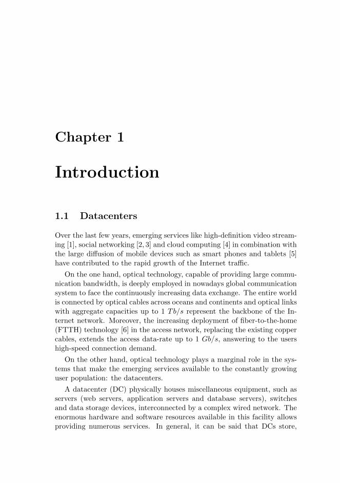
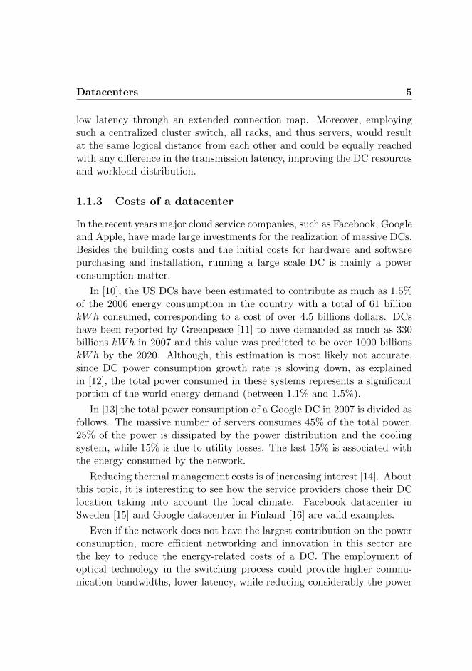
A large-scale DC, addressed also as a warehouse-scale computer (WSC) [9],hosts over 100000 servers. The typical intra-DC network is a canonicalfat-tree architecture, as depicted in Figure 1.1.
Figure 1.1: Typical DC fat-tree topology network
Servers are arranged in racks and several racks are grouped together intoclusters. Servers of the same rack are interconnected by so-called top-of-the-rack (TOR) switches, while inter-racks and inter-clusters communications
Datacenters 3
are handled by cluster switches at the second hierarchical level of the DCarchitecture. Depending on the size of the DC, an extra aggregation layer,which employs high data-rates switches, may be present on top of the clusterlevel.
This architecture has two main advantages: it can be easily scaled and itis fault tolerant (a TOR switch is usually connected to two or more clusterswitches). However, this network topology presents also some drawbacks.A high number of interconnection links is required. Moreover, the switchingprocess is performed by electronic packet switches, while server-to-switchand switch-to-switch links rely on optical technology. This translates inhigh power consumption of the TOR and cluster switches, mainly caused bythe optical-to-electrical (O-E) and electrical-to-optical (E-O) transceiversand by the power consumed by the electronic switch fabrics like crossbarswitches, buffers and high speed serializer/deserializer (SerDes). For thesame reason, the system is affected by high latency. Servers placed in dif-ferent racks are affected by communications lags. Packets travelling acrossthe DC network experience multiple O-E and E-O conversions and the la-tency is affected by the implicit queueing time due to the store-and-forwardprocessing at each switching node. Moreover, there is a communicationbottleneck between the different levels of the DCs fat-tree architecture.Typically, a rack hosts up to 40 servers (in the form of blades), while acommonly employed TOR switch features 48 ports. It is clear that onlya portion of the TOR switches bandwidth is available for inter-rack com-munications (the typical subscription ratio is 1/5), limiting the possibilityof communication bandwidth between different racks or clusters. A similarlimitation exists between the cluster and the aggregation layers. This issueis more evident during the communications between servers placed at theedges of the bottom layer of the current DC topology since the transmittedpackets have to climb up and down the fat-tree architecture to reach theirdestination.
1.1.2 A future scenario
As the DCs continue to increase to sustain the emerging services, whichrequire intense interactions among the servers and increasing computationalpower, more efficient interconnections are required.
Theoretically, flattening the intra-DC network, providing full bidirec-
4 Datacenters
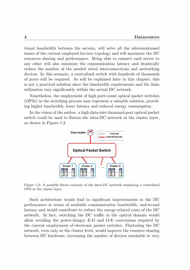
tional bandwidth between the servers, will solve all the aforementionedissues of the current employed fat-tree topology and will maximize the DCresources sharing and performance. Being able to connect each server toany other will also minimize the communication latency and drasticallyreduce the number of the needed wired interconnections and networkingdevices. In this scenario, a centralized switch with hundreds of thousandsof ports will be required. As will be explained later in this chapter, thisis not a practical solution since the bandwidth requirements and the linksutilization vary significantly within the actual DC network.
Nonetheless, the employment of high port-count optical packet switches(OPSs) in the switching process may represent a valuable solution, provid-ing higher bandwidth, lower latency and reduced energy consumption.
In the vision of the author, a high data-rate thousand-port optical packetswitch could be used to flatten the intra-DC network at the cluster layer,as shown in Figure 1.2.
Figure 1.2: A possible future scenario of the intra-DC network employing a centralizedOPS at the cluster layer.
Such architecture would lead to significant improvements in the DCperformance in terms of available communication bandwidth, end-to-endlatency and would contribute to reduce the energy-related costs of the DCnetwork. In fact, switching the DC traffic in the optical domain wouldallow avoiding the power-hungry E-O and O-E conversions required bythe current employment of electronic packet switches. Flattening the DCnetwork, even only at the cluster level, would improve the resource sharingbetween DC hardware, increasing the number of devices reachable in very
Datacenters 5
low latency through an extended connection map. Moreover, employingsuch a centralized cluster switch, all racks, and thus servers, would resultat the same logical distance from each other and could be equally reachedwith any difference in the transmission latency, improving the DC resourcesand workload distribution.
1.1.3 Costs of a datacenter
In the recent years major cloud service companies, such as Facebook, Googleand Apple, have made large investments for the realization of massive DCs.Besides the building costs and the initial costs for hardware and softwarepurchasing and installation, running a large scale DC is mainly a powerconsumption matter.
In [10], the US DCs have been estimated to contribute as much as 1.5%of the 2006 energy consumption in the country with a total of 61 billionkWh consumed, corresponding to a cost of over 4.5 billions dollars. DCshave been reported by Greenpeace [11] to have demanded as much as 330billions kWh in 2007 and this value was predicted to be over 1000 billionskWh by the 2020. Although, this estimation is most likely not accurate,since DC power consumption growth rate is slowing down, as explainedin [12], the total power consumed in these systems represents a significantportion of the world energy demand (between 1.1% and 1.5%).
In [13] the total power consumption of a Google DC in 2007 is divided asfollows. The massive number of servers consumes 45% of the total power.25% of the power is dissipated by the power distribution and the coolingsystem, while 15% is due to utility losses. The last 15% is associated withthe energy consumed by the network.
Reducing thermal management costs is of increasing interest [14]. Aboutthis topic, it is interesting to see how the service providers chose their DClocation taking into account the local climate. Facebook datacenter inSweden [15] and Google datacenter in Finland [16] are valid examples.
Even if the network does not have the largest contribution on the powerconsumption, more efficient networking and innovation in this sector arethe key to reduce the energy-related costs of a DC. The employment ofoptical technology in the switching process could provide higher commu-nication bandwidths, lower latency, while reducing considerably the power
6 Optics in datacenters
consumptions [17–20]. According to the study in [21], the employment ofoptical interconnects within a DC would provide, over a period of 10 years,energy savings for over 150 million dollars.
A clear requirement for the employment of optical switches in a DCnetwork is that such devices should provide limited power consumption,limiting the networking costs.
1.2 Optics in datacenters
In current DCs, optical technology is employed only for point-to-point inter-connections between servers and TOR switches and between TOR switchesand cluster switches. In particular, short optical links are based on cost-effective multi-mode fibers (MMFs). Servers and TOR switches are inter-connected by Small Form-factor Pluggable transceivers (SFPs) at 1 Gb/s,while TOR-cluster switches communications relies on SFPs+ at 10 Gb/s.Due to the short-reach distances required, low-power and inexpensive ver-tical cavity surface emitting lasers (VCSELs) at 850 nm are employed.Higher bandwidth transceivers are already available, such as 4 × 10 Gb/sQSFPs (Quad-SFPs). Due to modal dispersion, VCSEL-based transceivershave limited reach-bandwidth product. The maximum reach at 10 Gb/s isaround 300 m. The maximum reach decreases if higher data-rate is con-sidered. The choice on the employed optical technology is mainly drivenby the low costs and power consumption of the devices, due to the largenumber of transceivers required. In a DC, distances beyond 300 m at 10Gb/s are covered by more expensive and higher-power transceivers based ondistributed feedback (DFB) lasers, in combination with single-mode fibers(SMF). DFB-based transceivers can be employed to increase interconnec-tion bandwidth and reach at the expense of higher power and costs.
As the DC bandwidth requirements continue to increase, the employ-ment of wavelength division multiplexing (WDM) represents a valid ap-proach to sustain the DC traffic volumes, in particular for long links asthe ones at the clusters layer [22]. WDM is widely employed in metroand long-haul transmissions. In a WDM system, multiple high data-ratewavelength channels co-propagate within the same optical SMF. Experi-mental results achieved transmission of over 100 Tb/s in a single SMF [23].Basically, a WDM transceiver operates with multiple transmitter-receiver
Optical datacenter: requirements and challenges 7
pairs on different WDM channels contained in the same optical fiber. In aDC environment this will result in an enormous advantage in scaling thebandwidth of the network. Once the SMF is deployed, as the number ofwavelength channels or the data-rate per channel is increased the networkbandwidth is greatly enhanced. To increase the network bandwidth in aMMF-based system, more parallel fibers have to be rolled out, increasingthe number of interconnections and the installation costs.
WDM is considered too costly for the data-rate currently in use in DCs.However, it may represent the only possible solution when scaling furtherthe bandwidth (e.g. 400 Gb/s) in particular for the aggregated traffic atthe clusters layer, and for distances beyond 300 m to be bridged in largerDCs.
It may be expected that the intra-DC network follows the same evo-lution of the telecommunication networks. Long-haul networks and metroarea networks (MAN’s) have evolved from traditional opaque networks intoall-optical networks. This evolution was driven by the issues caused by therapid growth of those networks. In an opaque network, the optical sig-nals undergo optical-to-electrical-to-optical (O-E-O) conversions at eachrouting node. This translates, for continuously increasing bandwidths anddistances, in higher costs, heat dissipation, power consumption and highoperation and maintenance costs. On the contrary, all-optical networks,in which optical cross-connects and reconfigurable optical add/drop multi-plexers (ROADM) are employed, provide higher bandwidth, reduced powerconsumption and reduced operation costs [24].
1.3 Optical datacenter: requirements and chal-lenges
To realize a more efficient intra-DC network (in terms of bandwidth, powerconsumption, latency and interconnection capabilities between the DC re-sources) optical packet switches (OPSs) have captured the attention ofmany research groups.
The advantage of using a transparent optical network and the issuescaused by the currently employed fat-tree architecture have already beendiscussed. Flattening the DC architecture employing an OPS capable ofoptically interconnecting the massive number of servers of a WSC would
8 Optical datacenter: requirements and challenges
solve the fat-tree architecture issues and provide the benefits of a transpar-ent optical network.
In principle, an all-to-all interconnection network between the servers ofa DC is the best solution to maximize the resources sharing and minimizethe latency of the systems. Interconnecting all the servers of a DC willrequire a centralized OPS with hundreds of thousands of ports. However,this is not a practical solution. In fact, the bandwidth requirements ofthe actual DC architecture differ as function of the considered hierarchicallevel. A clear understanding of DC traffic characteristics is a crucial pointfor designing an efficient and cost-effective intra-DC network.
1.3.1 Datacenter traffic features
DCs offer a large variety of services and in general three distinct classes ofDC can be identified: private DCs, university campus DCs and cloud com-puting DCs. Traffic within all these systems shows some common features(average packet size, for example), while other characteristics (as applica-tions or traffic flows) are quite different as function of the environment.
There are few publications available on this topic based on measurementsof real DCs [25–27]. The most interesting findings for the network designare the following. A traffic flow is defined as an established connectionbetween two servers.
- Traffic flow locality: describes the direction of the traffic. Packetsgenerated by a server may be directed to servers of the same rack(intra-rack flow) or to servers placed in a different rack (inter-rack orinter-cluster flow). This traffic feature is environment-dependent. Ineducational DCs intra-rack traffic ranges between 10% to 40% of thetotal traffic, while it’s up to 80% in cloud computing DCs. However,inter-rack and inter-cluster traffic (also known as east-west traffic) iscontinuously growing [28]. In WSCs, it is at the cluster level wherethe most traffic is confined [9]. In case of high inter-rack traffic, highbandwidth is required between racks while cost-effective commodityswitches can be employed for intra-rack communications.
- Link utilization: in all DC classes, the link utilization inside the rackand between racks is quite low. For 95% of the operations the band-width utilization is below 10% and it is below 30% for 99% of the
Optical datacenter: requirements and challenges 9
time. It sounds reasonable that the 1 Gb/s links employed to inter-connect the servers of the same rack would be able to sustain alsothe future traffic demand. Thus, intra-rack communications are notthe main issue in a DC environment. On the contrary, the utilizationof inter-cluster links and at the aggregation layer is high and higherbandwidth is a near requirement.
- Traffic flow size and duration: the majority of the traffic flows aresmall (≤ 10 kB) and last for few hundreds of milliseconds. This trafficfeature affects the choice of the network architecture and the choiceof the switch fabric. If most of the traffic has a long duration (secondsor tens of seconds), then an optical device with high reconfigurationtime could be employed in the switching process. This is not the casefor a DC environment.
- Packet size: DC traffic shows a bimodal distribution around the min-imum and the maximum Ethernet frame size (40 and 1500 bytes).This phenomenon is due to the fact the packets are generally smallcontrol packets or portions of large files that are exchanged betweenthe DC storage facilities.
These empirical results reveal that it is not necessary to interconnectall the servers of a DC in a flat network. However, even interconnectingonly the clusters of a WSC by means of an OPS, a large number of switchinput/output ports is required. In addition, the traffic characteristics makethe employment of a fast reconfigurable OPS a necessity. Those are notthe only challenges in implementing an optical DC network.
1.3.2 Lack of optical memories
The employment of an OPS that transparently switches packets in theoptical domain avoiding O-E-O conversion is very challenging. Electronicpacket switches employ input and output buffering to perform the store-and-forward processing needed at each switching node. This is impossibleto implement in the optical domain, for the simple reason that an opticalrandom access memory (RAM) does not exist.
Two approaches are commonly used to overcome the lack of opticalRAM. Several studies [29, 30] rely on the employment of fiber delay linebased buffers to store signals in the optical domain. Basically, in case of
10 Optical datacenter: requirements and challenges
contention at the switch, one of the packet contending the output port isswitched to a fiber delay line (FDL). After a fixed time delay, dependenton the length of the used FDL, the packet is fed again at the input of theswitch. However, this approach increases significantly the complexity ofthe switch architecture and its control. As a consequence, extra-latency isintroduced in the system. Moreover, this method affects the signal powerand the fact that the packet can be delayed only for fixed delay times doesnot solve the problem completely.
The second approach consists in confining the buffering process at theedges of the switching network [31]. In this case the buffering is performedin the electrical domain by employing commonly used electronic buffers,while the switching process is kept transparent in the optical domain. Theemployment of an OPS with fast reconfiguration times becomes importantto reduce the needed buffer capacity. Moreover, this method can be ap-plied only in systems that feature short host-switch distances. In case ofcontentions, in fact, the packets stored at the edge of the switch need to beretransmitted. This process affects the system latency, that is basically de-pendent on the number of contentions and on the link length. Fortunately,intra-DC networks feature links that range from few to hundreds meters.
The employment of WDM technology would benefit the DC network alsoin this context. In fact, it would enable the opportunity to reduce the packetcontentions exploiting the optical domain. Wavelength converters (WCs)could be used to solve contentions “on-the-fly” in the optical domain. Inother words, since many wavelength channels can co-propagate in a singleoptical fiber, converting the contended packet to a different and availablewavelength would reduce the number of contentions and increase the systemthroughput. High data-rate WCs have already been demonstrated [32].
1.3.3 Latency
The actual DC network is affected by high latency due to the store-and-forward processing needed at each routing node of the network. Thesedelays are dependent on the physical position of the packets destinationtarget. Inter-rack communications delays can be in the 100 µs order whilefew more hundreds µs have to be added for inter-cluster communicationdelays [9].
Besides the intrinsic advantage in speed provided by the use of optical
Optical datacenter: requirements and challenges 11
signals over electronics, the choice of the switch architecture and technologyplays an important role in this context. For example, switching fabricsthat features high configuration times, as optical micro electro-mechanicalsystems (MEMS) based switch, are not suited for optical packet switchingin DC networks.
Summarizing the previous considerations, the desired optical packetswitch has not only to handle a large number of high data-rate input/outputports, but needs to add negligible latency to the intra-DC communicationnetwork.
1.3.4 Photonic integration
Limited power consumption is one of the requirements to employ an OPSin a intra-DC network. Reducing the optical switch footprint will result indiminished power consumption and reduced operation and fabrication costs.The only approach to reach this goal is by means of photonic integration.
Photonic integration technology enables the opportunity to incorporatemultiple photonic functions on a single chip. The main advantages of fab-ricating photonic integrated circuits (PICs) over the use of discrete opticalcomponents are: reduced system footprint, reduced power consumption,reduced fiber coupling losses and reduced packaging costs, since many com-ponents can be co-fabricated on a single device.
Despite the multi-decennial research in this field, few market-orientedPICs are available. The reason of this low diffusion can be found in thelack of a fabrication standard [33]. To overcome this issue, fabricationplatforms, that employ a small set of standardized technologies, have beendeveloped [34, 35].
Unlike electronic integrated circuits, where silicon is the dominant ma-terial, PICs are being fabricated employing heterogeneous materials. III-Vsemiconductors and in particular Indium Phosphide (InP) [36], silica on sil-icon, namely photonic lightwave circuit (PLC) [37] and silicon on insulator(SOI) [38] are the most used material systems.
Each material can provide different advantages and limitations depend-ing on the desired photonic functionality to integrate. Low losses and lowthermal sensitivity make PLC suitable for the integration of passive pho-tonic circuits. For instance, PLC has been widely employed for the fabrica-
12 Optical packet switches: state of the art
tion of integrated array waveguide gratings (AWGs) [39, 40]. However, thisplatform does not allow the small footprint achievable by the other mate-rials. InP is perhaps the most versatile material platform since it allowsthe integration of both passive and active functionalities on the same chip.Waveguides, light sources, modulators and amplifiers can be co-integratedon the same device allowing the fabrication of high-complexity PICs [41, 42].SOI chips are promising for their limited footprint size and the CMOS com-patibility of their fabrication process [43], while active functionalities on thismaterial are still an open challenge.
To exploit the advantages and overcome the limitations of the differentmaterial platforms, hybrid solutions have been considered [44–48].
The requirements and the challenges described in this section repre-sent the motivations of this thesis. This work aims to investigate, studyand implement an OPS architecture for intra-DC networks. The scenariodepicted in Figure 1.2 has to be considered as the starting point of thisresearch. The desired OPS has not only to be capable of handling a largenumber (≥ 1000) of high data-rate input/output ports but it has to addextremely low latency to the system (≤ 1µs) and its integration should befeasible.
1.4 Optical packet switches: state of the art
In the last decade, many research groups have focused on the implementa-tion of multi-port optical switches. In this work, the interest is not only onthe switch port-count, but it is also on the switching speed. Switches basedon optical MEMS [49] or thermo-optic [50], although capable of switchinghigh data-rates and of scaling to relatively high port-count, are not takeninto account in this section due to their limited switching speed.
The most important attempt to realize a large port-count OPS is perhapsthe OSMOSIS project [51]. A broadcast and select switching architecturefor high performance computing (HPC) applications was implemented byusing optical switches based on semiconductor optical amplifiers (SOAs).While the optical switches used in the system could be switched betweenthe on and off state in few nanoseconds, the overall response time wasmuch slower due to the controller complexity. Moreover, the costs of theswitch implementation were too high due to the high number of components
Preview of the thesis 13
required.
Several integrated multi-port switches have been presented. In [52] amonolithically integrated 16 × 16 InP switch is presented. The switch re-lies on a Benes architecture based on SOAs and can provide a maximumthroughput of 640 Gb/s. The MOTOR device [53] is an 8 × 8 InP mono-lithically integrated optical switch based on tunable wavelength converters.In [54, 55] an InP integrated 1 × 16 optical switch has been presented. Itcan simultaneously handle both on off keying (OOK) and differential phaseshift keying (DPSK) modulated data packets. In [56], this concept is scaledto a 1 × 100 optical switch. The IRIS project [57] demonstrated a multi-stage architecture based on a combination of space switches and wavelengthrouting switches that utilize fast wavelength converters and 40 × 40 arraywaveguide gratings (AWGs). Another interesting approach to switching isthe one adopted in the vortex switch [58]. Multi-wavelength packets aredelivered to the destination through concentric loops of optical nodes. Inthe SPINet network [59] packets are routed through an Omega architecturebased on 2 × 2 switching nodes. In [60] a qualitative categorization andcomparison of optical interconnects for DC applications is reported.
Although the referred works show a great progress in technology devel-opment in this field, these devices still feature a relatively low number ofports. Moreover, many of them have not yet been demonstrated in a systemenvironment.
1.5 Preview of the thesis
The goal of this work is to identify, study and implement an optical packetswitch architecture for high performance data center networks. Large port-count, high data-rate per port and low reconfiguration time are the mainrequirements taken into account to reach this goal. Such a switch willallow flattening the data center network enhancing the resources sharingcapabilities within these systems, providing higher bandwidth and reducingthe system latency and costs.
In Chapter 2, a novel architecture is presented. The choice on the archi-tecture is motivated by the study of the effects of switch architectures onthe intra-DC network performances. A novel single-chain analytic modelis used as a tool to compute system latency and throughput as function of
14 Preview of the thesis
the employed switch architecture and as function of the switch port-count.An ideal and a practical implementation of the proposed OPS architectureare presented in this chapter.
The novel architecture is based on a strictly non-blocking architecture.The switch operates transparently in the optical domain while being elec-tronically controlled. The lack of optical random access memory is over-come by confining the buffering process at the edges of the switching ma-trix, where it can be performed electronically. The proposed architecturefeatures a modular structure. The modules operate in parallel and au-tonomously by each other. Wavelength division multiplexing is employedto scale the architecture to a large port-count, thus the number of effec-tive interconnections is given by the number of input fiber F multiplied bythe number of wavelength channels carried by each fiber M . Wavelengthconversion is employed to avoid contentions between packets coming fromdifferent input fibers and directed to the same output port, enabling theautonomous and parallel operations of the modules.
Each module requires several functional blocks:
• Channel demultiplexer: to demultiplex the M channels carried byeach input fiber.
• Label extractor: to extract the packet label of each WDM channel.
• Label processor: to identify the packet destination.
• 1 × F optical switch: to forward the packet payload of each WDMchannel to the appropriate output port.
• Switch controller: to drive the optical switch according to the packetdestination, to solve contentions and to generate acknowledge messagefor the transmitting nodes.
• M × 1 wavelength selector: to select one out of a maximum of Mpackets in case multiple packets coming from the same input fiber(and thus handled by the same module) have the same destination.Controlled by the switch controller.
• Fixed wavelength converter: to convert the packets to a fixed wave-length in order to avoid contentions between different modules.
Flow control enables packet retransmission of packets dropped by thewavelength selector. The modular structure of the architecture allows em-ploying highly distributed control. Each module can be autonomously con-
Preview of the thesis 15
trolled. This, in combination with in-band parallel labelling and label pro-cessing techniques, results in nanosecond reconfiguration time, minimizingthe buffering needed at the edges of the switch and reducing the added la-tency associated with the packet retransmissions. Also, the modular struc-ture allows investigating the architecture performances studying a singlemodule subsystem.
In Chapter 3, the performances of the novel architecture, in terms of la-tency, packet loss and throughput are investigated by means of simulationsof the OPS in an intra-DC environment. Systems employing switches withdifferent port-count are considered as well as synchronous and asynchronousoperations. The effects of the buffer capacity on the network performancesare also investigated in this chapter.
In Chapter 4, the first implementation of the proposed OPS architec-ture (without the flow control functionality) and its controller is presented.The dynamic switching performances are investigated employing two dis-tinct experimental set-up. In the first experiment, a single 1× 8 switchingmodule is implemented by employing discrete optical components. In thesecond experiment, an integrated 1× 4 optical cross-connect is used to in-vestigate the possible integration of the OPS. In both cases, an in-bandlabeling technique, which allows “on-the-fly” parallel packet labels detec-tion is employed. The in-band packets labels, after being extracted from thepayload, are O-E converted and detected by a dedicated electronic circuitryand finally processed by the switch controller. The switch controller is real-ized by programming a field-programmable gate array (FPGA) board, thatis employed to solve possible contentions and to drive the OPS module.
In Chapter 5, two distinct flow control implementations are presented.The OPS switch architecture with a FPGA-based flow control performancesare investigated in an experimental set-up. This implementation requiresa dedicated electronic network to enable the flow control functionality. Toovercome the impairments due to the employment of a distinct network forthe flow control process in a large scale system as a DC, the implementationof an all-optical flow control is studied with promising results. This imple-mentation relies on the re-utilization of part of the extracted label power togenerate an optical acknowledge message by appropriately driving a SOA.The acknowledgement is sent back to the transmitting node on the sameoptical link employed for the packet transmission. Thus, using this method,there is no need of a dedicated network for the flow control process.
16 Novel contributions
In Chapter 6, further steps towards the total integration of the OPSarchitecture are taken. The employment of a microring resonators arrayas in-band label extractor for the proposed architecture is investigated.The employed device is able to successfully extract multiple in-band labelwavelengths with limited penalty on the packet payload. Moreover, the em-ployment of a channel demultiplexer and a microring-based label extractorintegrated on a single device is exploited. Also, the integration of the otherfunctional blocks required by each architecture module is discussed in thischapter.
Finally, Chapter 7 presents the conclusions of this work. The main re-sults are summarized. Considerations about port-count scalability, latency,data-rate, throughput, integration and power consumption of the proposedswitch architecture are given in this chapter. Also, alternative approachesand recommendations regarding future research related to the work pre-sented in this thesis are reported.
1.6 Novel contributions
1. A simple analytic model that allows computing the latency and thethroughput of a system as function of the employed switch architec-ture is presented. The model is used as a tool to identify a suitableOPS architecture for intra-DC networks.
2. A novel WDM optical packet switch architecture for intra-DC net-works is presented. The main advantage of the selected architectureis its modular structure that enables the employment of a highlydistributed control system. The optical switching modules operatein parallel and independently, due to the employment of wavelengthconverters that avoid inter-module contentions. This allows to re-duce the overall switch reconfiguration time to the time to configurea single module.
3. The proposed architecture performances in a DC environment areinvestigated for the first time by means of simulations. Promisingperformances are provided under all traffic conditions simulated. Sys-tems with port-count ranging from 4 to 1024 ports are simulated toinvestigate the scalability of the proposed architecture. Interestingresults on the effects of the buffer capacity on the performances are
Novel contributions 17
reported.
4. The feasibility of a 64 × 64 OPS based on the proposed architectureemploying discrete optical components is demonstrated. Althoughnot full-functional (the flow control mechanism is not implemented),the 1 × 8 switching module and its controller are tested successfullyin a experimental set-up injecting in the module 8 × 40 Gb/s WDMchannels.
5. The feasibility of a 16 × 16 OPS based on 1 × 4 optical integratedcross-connect modules is demonstrated by injecting in the photonicchip 4×40 Gb/s WDM channels. Dynamic switching capabilities anderror free operation are shown.
6. Two possible implementations of the controller flow control function-ality are presented. An FPGA-based and an all-optical solution forthe flow control system are tested in experimental set-up with promis-ing results.
7. Further steps towards the total integration of the OPS architectureare taken investigating the employment of a integrated label extractorand an integrated WDM channels demultiplexer and label extractorsuitable for the studied OPS architecture.

Chapter 2
Novel OPS architecture
In this chapter1, a novel optical packet switch (OPS) architecture suit-able for intra-DC network is presented. Motivations on the choice of theproposed OPS architecture are presented in combination with an analyticstudy of the effects of the switch architectures on the intra-DC networkperformances.
2.1 System under investigation
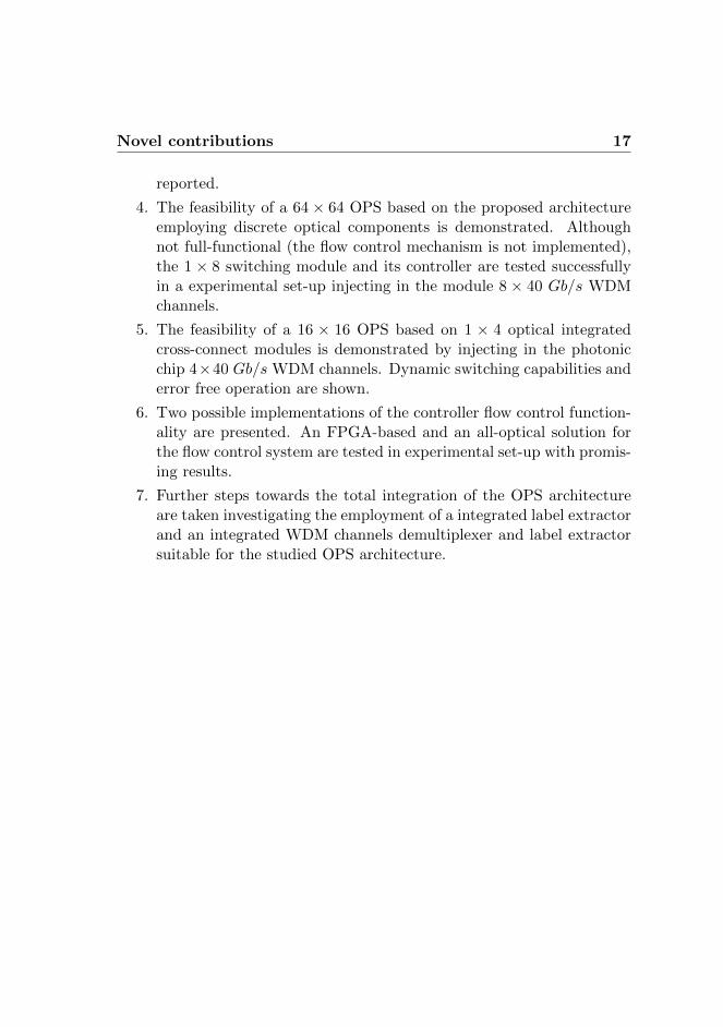
This chapter aims at identifying an OPS architecture that is capable ofoptically interconnecting over thousand ports while being controllable innanosecond time scales. The scenario described in Section 1.1.2 representsthe starting point of this research. The future intra-DC network is assumedto feature a centralized thousand-port OPS which is employed to flatten theDC cluster layer. In this scenario, intra-rack and intra-cluster communica-tions are managed by the pre-existing reliable and cost-efficient electronicswitches, while inter-cluster communications are handled by the OPS. Thesystem under investigation is depicted in Figure 2.1.
The OPS interconnects a number of ingress clusters with a number ofegress clusters by means of high bit-rate input/output ports. The switch
1based on the research and the results published in: S. Di Lucente, N. Calabretta,J.A.C. Resing, and H.J.S Dorren, “Scaling low-latency optical packet switches to a thou-sand ports”, IEEE/OSA Journal of Optical Communication and Networking, vol. 4, no.9, pp. A17-A28, 2012. [61]
20 System under investigation
Figure 2.1: Schematic system under investigation; OPS placed at cluster level of a DC.
is assumed to operate transparently in the optical domain, thus no optical-to-electrical (O-E) and electrical-to-optical (E-O) conversions at the inputsand outputs of the switch are required. The buffering is confined at theedges of the switching matrix, where it is electronically performed.
2.1.1 Architectures control issue
Many architectures can be used to implement an OPS. Despite many re-search groups are focusing on this topic since many years, scaling an OPSarchitecture to a large port-count is an open challenge, as discussed inChapter 1. Many technological impairments can limit the number of portsof such architectures. However, what is often overlooked is the impact ofthe adopted switch architecture on the switch control time. In this respect,this section focus on the effects of the employed switch architecture on theswitch reconfiguration time.
Realizing an optical packet switch that takes too long to be reconfiguredwill limit the system performance, requiring large buffers at the edges of theswitching network and affecting the system operations in terms of latencyand throughput. The following considerations are valid for the studiedswitch architectures regardless the technologies used for their implementa-tions.
To facilitate the discussion, the focus is on synchronous switching opera-
System under investigation 21
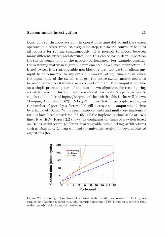
tions. In a synchronous system, the operation is time slotted and the systemoperates in discrete time. At every time step, the switch controller handlesall requests for routing simultaneously. It is possible to choose betweenmany different switch architectures, and this choice has a deep impact onthe switch control and on the network performance. For example, considerthe switching matrix in Figure 2.1 implemented as a Benes architecture. ABenes switch is a rearrangeable non-blocking architecture that allows anyinput to be connected to any output. However, at any time slot in whichthe input state of the switch changes, the entire switch matrix needs tobe reconfigured to establish a new connection map. The computation timeon a single processing core of the best-known algorithm for reconfiguringa switch based on this architecture scales at least with N log2N , where Nequals the number of inputs/outputs of the switch (this is the well-known“Looping Algorithm”, [62]). N log2N implies that, in principle, scaling upthe number of ports by a factor 1000 will increase the computational timeby a factor of 10,000. While small improvements and multi-core implemen-tations have been considered [63–65], all the implementations scale at leastlinearly with N . Figure 2.2 shows the configuration times of a switch basedon Benes architecture (different rearrangeable non-blocking architecturessuch as Banyan or Omega will lead to equivalent results) for several controlalgorithms [66].
Figure 2.2: Reconfiguration time of a Benes switch matrix expressed in clock cyclesemploying a looping algorithm, a trial partition machine (TPM), and an algorithm thatscales linearly with the switch port-count.
22 System under investigation
The horizontal axis shows the number of inputs and outputs of theswitching matrix, while the vertical axis shows the number of clock cy-cles needed to set the connection map. Assuming that a single clock cycletakes 1 ns, Figure 2.2 indicates that a 1024-port Benes switch architecturewith a scheduler employing the looping algorithm requires more than 10µs to be configured. During the configuration time, the switch is unable tohandle data; thus incoming packets are either lost or need to be stored inelectronic buffers, increasing the link latency and limiting the throughputof the system. Assuming that some services in a DC environment allowa maximum latency of 1 µs, it can be concluded that, if the number ofswitch ports exceeds a critical threshold, the switch is no longer capableof handling the incoming switching requests within the maximum latencyallowed in the system.
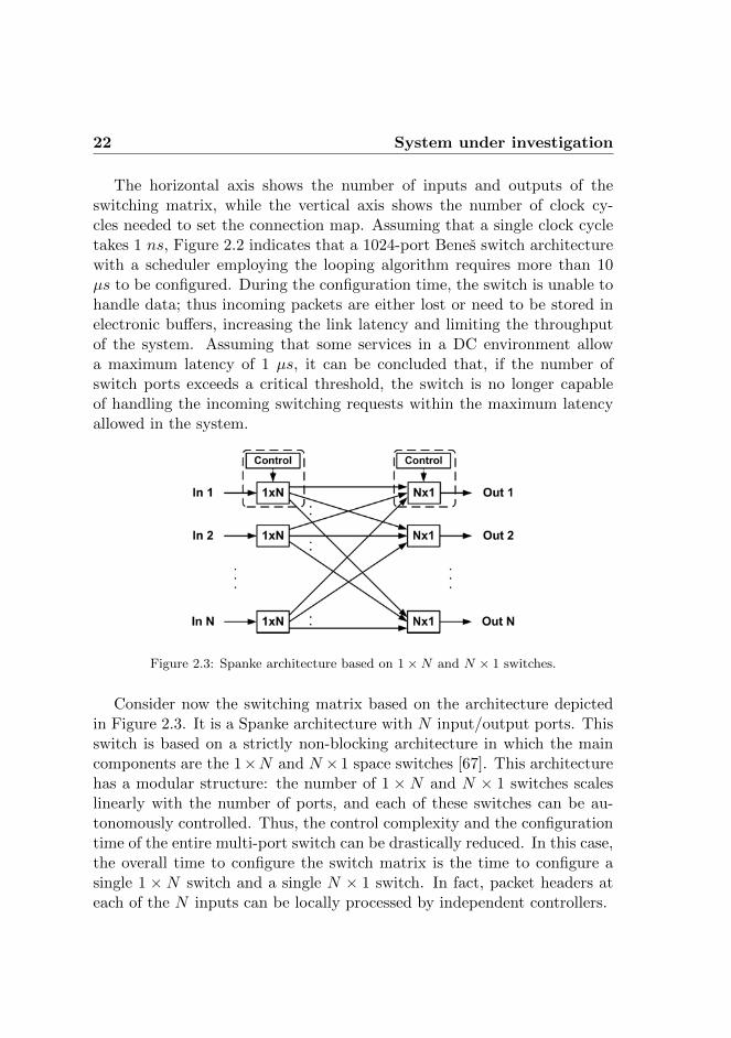
Figure 2.3: Spanke architecture based on 1 ×N and N × 1 switches.
Consider now the switching matrix based on the architecture depictedin Figure 2.3. It is a Spanke architecture with N input/output ports. Thisswitch is based on a strictly non-blocking architecture in which the maincomponents are the 1×N and N ×1 space switches [67]. This architecturehas a modular structure: the number of 1 × N and N × 1 switches scaleslinearly with the number of ports, and each of these switches can be au-tonomously controlled. Thus, the control complexity and the configurationtime of the entire multi-port switch can be drastically reduced. In this case,the overall time to configure the switch matrix is the time to configure asingle 1 × N switch and a single N × 1 switch. In fact, packet headers ateach of the N inputs can be locally processed by independent controllers.
Single-chain model 23
2.2 Single-chain model
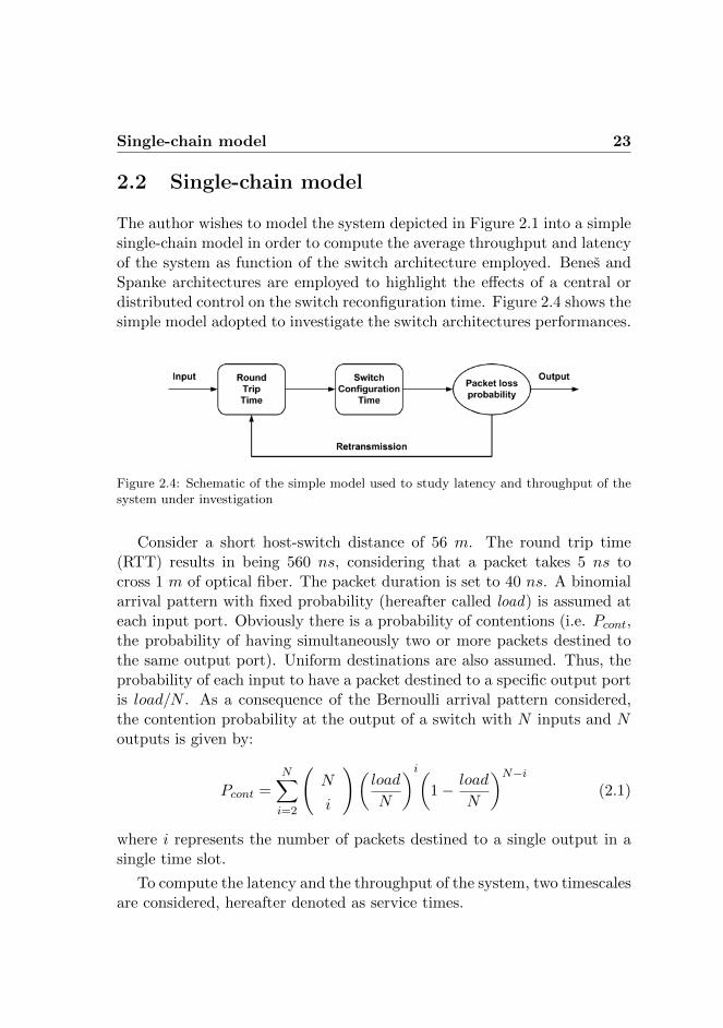
The author wishes to model the system depicted in Figure 2.1 into a simplesingle-chain model in order to compute the average throughput and latencyof the system as function of the switch architecture employed. Benes andSpanke architectures are employed to highlight the effects of a central ordistributed control on the switch reconfiguration time. Figure 2.4 shows thesimple model adopted to investigate the switch architectures performances.
Figure 2.4: Schematic of the simple model used to study latency and throughput of thesystem under investigation
Consider a short host-switch distance of 56 m. The round trip time(RTT) results in being 560 ns, considering that a packet takes 5 ns tocross 1 m of optical fiber. The packet duration is set to 40 ns. A binomialarrival pattern with fixed probability (hereafter called load) is assumed ateach input port. Obviously there is a probability of contentions (i.e. Pcont,the probability of having simultaneously two or more packets destined tothe same output port). Uniform destinations are also assumed. Thus, theprobability of each input to have a packet destined to a specific output portis load/N . As a consequence of the Bernoulli arrival pattern considered,the contention probability at the output of a switch with N inputs and Noutputs is given by:
Pcont =
N∑i=2
(N
i
)(load
N
)i(1− load
N
)N−i
(2.1)
where i represents the number of packets destined to a single output in asingle time slot.
To compute the latency and the throughput of the system, two timescalesare considered, hereafter denoted as service times.
24 Single-chain model
- The round trip time (RTT): this is the minimum time that a singlepacket spends in the system. The packet takes RTT/2 to reach theoutput, but it can be considered successfully delivered only after anacknowledgment message is received back by the input (taking againRTT/2).
- The configuration time of the switch (tswitch): this time delay dependson the architecture employed to realize the switch.
In addition, it has to be considered that the packets in the chain couldcontend the output port with the other N − 1 inputs. Consider a packetcoming from input 1 and destined to output N of the switch of Figure 2.1.There is a contention whenever a packet is present at input 1 and thereis at least one packet coming from the other N − 1 inputs addressed tothe same output port. When the packet experiences a contention and it isdropped (for output contentions in the Benes architecture and in case ofcontentions in the N × 1 switches for the Spanke architecture), it has to beretransmitted.
The packet takes RTT/2 to reach the output, and when it is successfullyreceived an acknowledge message is generated and sent back to appropriatesender, again taking RTT/2. If the sender does not receive the acknowledg-ment after RTT , the packet is automatically retransmitted. Retransmittingimplies serving the packet again; the packet is thus delayed by the servicetimes associated with RTT and tswitch. The retransmission probabilitydepends on the specific arrival pattern considered. The probability of con-tention for a given packet (Pcont gp) at one of the N inputs of the system,considering a Bernoulli arrival pattern and uniform destinations, can beexpressed as follows:
Pcont gp =
N−1∑k=1
(N − 1
k
)(load
N
)k(1− load
N
)N−1−k
(2.2)
where k represents the number of packets coming from the others N − 1inputs and destined to the same output port. Note that when k = 0 thereis no contention. When there are k packets arriving from the other N − 1inputs, our given packet loses the contention with a probability k/(k + 1).Equal priority is assumed for the packets here, so each packet has thesame probability of being the contention winner. Thus, the probability ofretransmission (PRetr), i.e. the probability that a packet is present at one
Single-chain model 25
input, experiences a contention, and loses it is given by:
PRetr = load ·N−1∑k=1
(N − 1
k
)(load
N
)k(1− load
N
)N−1−k k
k + 1(2.3)
where load represents the probability of having a packet at the consideredinput.
The probability of retransmission expressed in Equation 2.3 affects loadat each of the input ports. After each RTT , the probability of having apacket at the input of the system is increased by PRetr, as expressed inEquation 2.4. After a RTT , the input load is increased by the packetsthat lost the contention at the output. This effect is taken into accountby the definition of real load (loadR). It is important to know that this isan approximation. In fact, once again uniform destinations for the packetsthat lose contentions are considered. In other words, load represents thetraffic injected in the system, while loadR represents the real traffic in thesystem, considering also the retransmitted packets.
loadR(i) = load+ PRetr(i− 1) (2.4)
This increment on the probability of having a packet at the input portaffects in turn the probability of retransmission, which becomes:
PRetr(i) = loadR(i) ·N−1∑k=1
(N − 1
k
)(loadR(i)
N
)k
·(
1− loadR(i)
N
)N−1−k k
k + 1
(2.5)
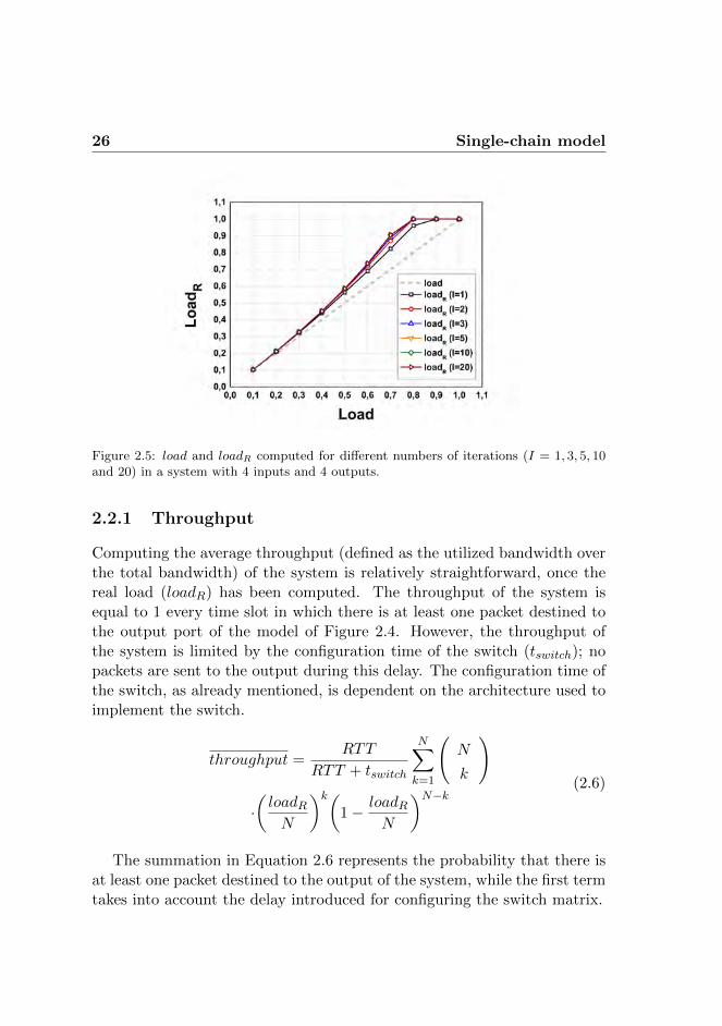
loadR can be recursively computed by using Equation 2.5 in Equation 2.4with the conditions (i) loadR(0) = load and (ii) 0 ≤ loadR(i) ≤ 1. Figure2.5 shows the behavior of loadR as function of load, considering differentnumber of iterations (I) in Equation 2.4 for a system with four input/outputports.
It is visible that, for a number of iterations larger than three, the changesare negligible. Figure 2.5 shows also that loadR is equal to 1, due to con-dition (ii), for load values around 0.8. Under these traffic conditions, thebuffers of a real system will be rapidly filled up and buffer overflowing willbecome unavoidable. However, it is important to note that the model doesnot take into account the buffer size, which is supposed to be infinite.
26 Single-chain model
Figure 2.5: load and loadR computed for different numbers of iterations (I = 1, 3, 5, 10and 20) in a system with 4 inputs and 4 outputs.
2.2.1 Throughput
Computing the average throughput (defined as the utilized bandwidth overthe total bandwidth) of the system is relatively straightforward, once thereal load (loadR) has been computed. The throughput of the system isequal to 1 every time slot in which there is at least one packet destined tothe output port of the model of Figure 2.4. However, the throughput ofthe system is limited by the configuration time of the switch (tswitch); nopackets are sent to the output during this delay. The configuration time ofthe switch, as already mentioned, is dependent on the architecture used toimplement the switch.
throughput =RTT
RTT + tswitch
N∑k=1
(N
k
)
·(loadRN
)k(1− loadR
N
)N−k(2.6)
The summation in Equation 2.6 represents the probability that there isat least one packet destined to the output of the system, while the first termtakes into account the delay introduced for configuring the switch matrix.
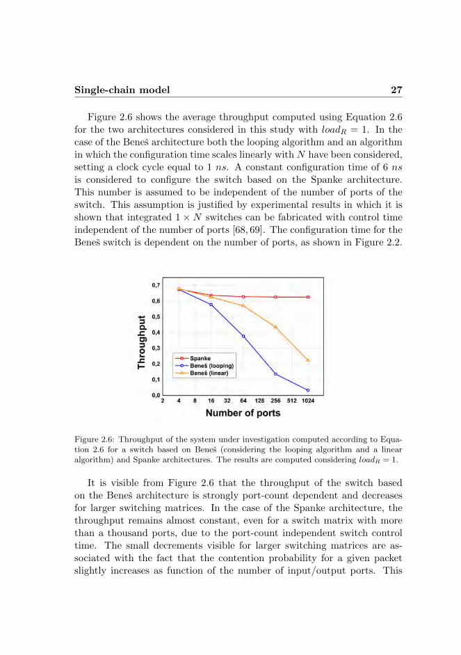
Single-chain model 27
Figure 2.6 shows the average throughput computed using Equation 2.6for the two architectures considered in this study with loadR = 1. In thecase of the Benes architecture both the looping algorithm and an algorithmin which the configuration time scales linearly with N have been considered,setting a clock cycle equal to 1 ns. A constant configuration time of 6 nsis considered to configure the switch based on the Spanke architecture.This number is assumed to be independent of the number of ports of theswitch. This assumption is justified by experimental results in which it isshown that integrated 1 ×N switches can be fabricated with control timeindependent of the number of ports [68, 69]. The configuration time for theBenes switch is dependent on the number of ports, as shown in Figure 2.2.
Figure 2.6: Throughput of the system under investigation computed according to Equa-tion 2.6 for a switch based on Benes (considering the looping algorithm and a linearalgorithm) and Spanke architectures. The results are computed considering loadR = 1.
It is visible from Figure 2.6 that the throughput of the switch basedon the Benes architecture is strongly port-count dependent and decreasesfor larger switching matrices. In the case of the Spanke architecture, thethroughput remains almost constant, even for a switch matrix with morethan a thousand ports, due to the port-count independent switch controltime. The small decrements visible for larger switching matrices are as-sociated with the fact that the contention probability for a given packetslightly increases as function of the number of input/output ports. This
28 Single-chain model
can be explained by plotting the contention probability for a given packetas function of the port-count N , as described by Equation 2.2.
2.2.2 Latency
Computing the latency is more complicated. This is due to the fact thatthe analytic model described in this section does not consider the size ofthe input buffer of the system, while the latency of the system stronglydepends on the buffer capacity. However, the aim of the model presented inthis section is to provide a simple and fast tool to compute the latency andthroughput of the studied system in order to obtain a general understandingof the node performance as function of the different architectures employedto realize the OPS.
The probability of retransmission is maximized (PRetrMax), consideringload = 1 in the summation of Equation 2.3 to compute the upper boundof the average system latency (latencyUB). Hence, the mean laencyUB canbe computed considering that:
latencyUB = RTT + tswitch + PRetrMaxlatencyUB (2.7)
or
latencyUB =RTT + tswitch
1− PRetrMax(2.8)
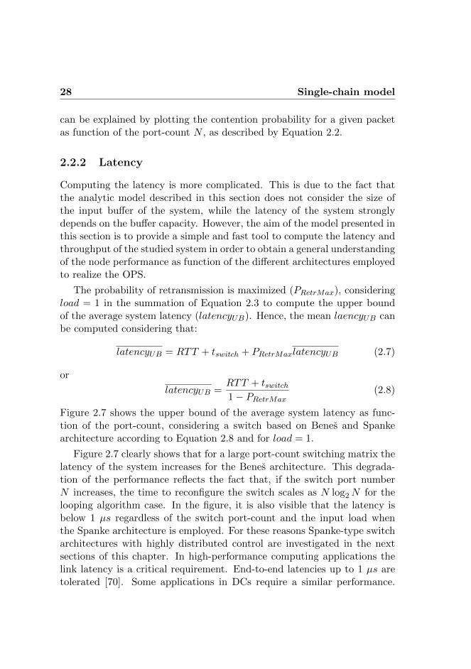
Figure 2.7 shows the upper bound of the average system latency as func-tion of the port-count, considering a switch based on Benes and Spankearchitecture according to Equation 2.8 and for load = 1.
Figure 2.7 clearly shows that for a large port-count switching matrix thelatency of the system increases for the Benes architecture. This degrada-tion of the performance reflects the fact that, if the switch port numberN increases, the time to reconfigure the switch scales as N log2N for thelooping algorithm case. In the figure, it is also visible that the latency isbelow 1 µs regardless of the switch port-count and the input load whenthe Spanke architecture is employed. For these reasons Spanke-type switcharchitectures with highly distributed control are investigated in the nextsections of this chapter. In high-performance computing applications thelink latency is a critical requirement. End-to-end latencies up to 1 µs aretolerated [70]. Some applications in DCs require a similar performance.
Novel architecture 29
Figure 2.7: Latency as a function of the port-count for a switching matrix based onBenes architecture employing the looping algorithm, and with configuration time thatscales linearly with the port-count, and for a switching matrix based on the Spankearchitecture as function of the number of ports. The results are computed consideringload = 1.
Thus, 1 µs will be considered as the maximum allowed latency in the sys-tem under investigation. Figure 2.7 shows also that, at full load, a Benesarchitecture cannot meet these requirements for port-count larger than 16,regardless of the switching speed. It is the switch control that limits theperformance of the system. Even if one is able to improve the control timeof the switch by making it scale linearly with the port-count, it is still notpossible to scale these switches to more than 64 ports while meeting thelatency requirements. For this reason, it is important to investigate switcharchitectures that have a configuration time port-count independent.
2.3 Novel architecture
The goal of this section is to individuate a switch architecture capable ofoptically interconnecting thousands of input and output ports and able toprovide very small end-to-end link latency. The strategy is to find a scalableswitch architecture with a control time that is port-count independent. Theform of distributed control that will be described allows for fast (few ns)
30 Novel architecture
reconfiguration of the switch matrix and on timescales that are indepen-dent of the number of ports. This approach will allow realizing switchingmatrices that can meet the latency requirements for DC applications.
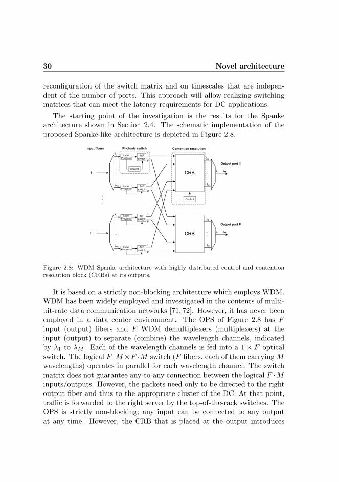
The starting point of the investigation is the results for the Spankearchitecture shown in Section 2.4. The schematic implementation of theproposed Spanke-like architecture is depicted in Figure 2.8.
Figure 2.8: WDM Spanke architecture with highly distributed control and contentionresolution block (CRBs) at its outputs.
It is based on a strictly non-blocking architecture which employs WDM.WDM has been widely employed and investigated in the contents of multi-bit-rate data communication networks [71, 72]. However, it has never beenemployed in a data center environment. The OPS of Figure 2.8 has Finput (output) fibers and F WDM demultiplexers (multiplexers) at theinput (output) to separate (combine) the wavelength channels, indicatedby λ1 to λM . Each of the wavelength channels is fed into a 1 × F opticalswitch. The logical F ·M×F ·M switch (F fibers, each of them carrying Mwavelengths) operates in parallel for each wavelength channel. The switchmatrix does not guarantee any-to-any connection between the logical F ·Minputs/outputs. However, the packets need only to be directed to the rightoutput fiber and thus to the appropriate cluster of the DC. At that point,traffic is forwarded to the right server by the top-of-the-rack switches. TheOPS is strictly non-blocking; any input can be connected to any outputat any time. However, the CRB that is placed at the output introduces
Novel architecture 31
connectivity, and thus a contention probability, between different channels.The CRB implementation is discussed later in this section.
It is important to mention that monolithically integrated 1 × 16 and1× 100 optical space switches that potentially support such schematic ar-chitecture have already been presented and tested [54, 56]. The 1 × 16(1 × 100) switch has been shown to operate almost penalty free for dif-ferent data formats at bit-rate up to 160 (10) Gb/s per channel, whereasthe time to configure the switch (∼ 5 ns) is independent of the number ofoutput ports. The results reported indicate that, for example, a 256× 256(F = 16,M = 16) OPS, implemented by using 1 × 16 switches as theone in [54] and considering 16 WDM channels at 160 Gb/s, could have anaggregate throughput which is larger than 40 Tb/s (16× 16× 160 Gb/s).
Introducing the employment of wavelength division multiplexing in theOPS architecture is a necessity. Consider for example to realize a 1024-portoptical switch based on a single-wavelength architecture. This will requirethe employment of 1024 1 × 1024 optical switches, which is not feasiblewith current technologies. Alternatively, a 1024-port optical switched basedon 32 wavelength channels architecture will similarly require 1024 1 × Fswitches, but now with F equal to 32. It has been already mentioned that1× F optical switches where F is larger than 32 have been presented [56].
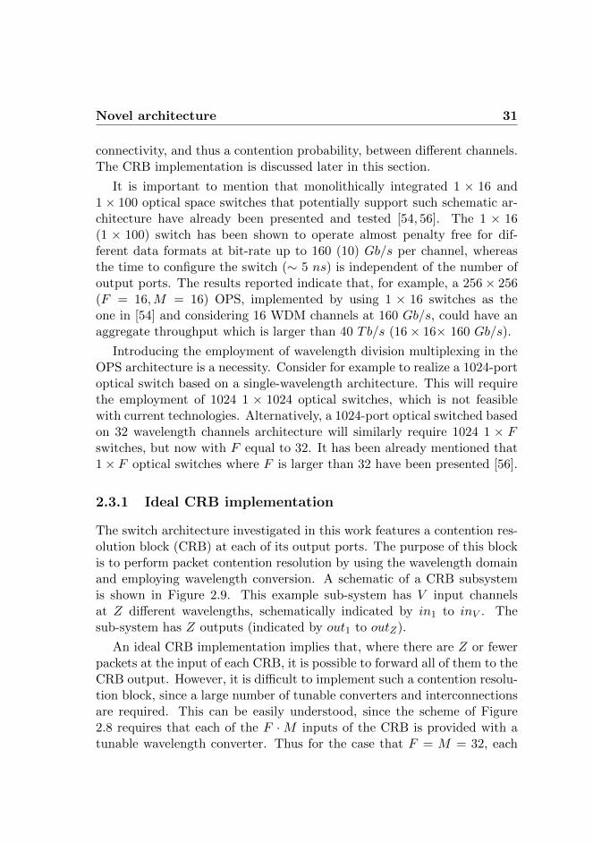
2.3.1 Ideal CRB implementation
The switch architecture investigated in this work features a contention res-olution block (CRB) at each of its output ports. The purpose of this blockis to perform packet contention resolution by using the wavelength domainand employing wavelength conversion. A schematic of a CRB subsystemis shown in Figure 2.9. This example sub-system has V input channelsat Z different wavelengths, schematically indicated by in1 to inV . Thesub-system has Z outputs (indicated by out1 to outZ).
An ideal CRB implementation implies that, where there are Z or fewerpackets at the input of each CRB, it is possible to forward all of them to theCRB output. However, it is difficult to implement such a contention resolu-tion block, since a large number of tunable converters and interconnectionsare required. This can be easily understood, since the scheme of Figure2.8 requires that each of the F ·M inputs of the CRB is provided with atunable wavelength converter. Thus for the case that F = M = 32, each
32 Novel architecture
Figure 2.9: Schematic of a CRB that can solve contentions by employing wavelengthconversion. It is assumed that there is a tunable converter at each input line.
output needs over 1000 tunable wavelength converters, requiring a largefootprint and large costs. Moreover, all the 1024 inputs of a CRB have tobe controlled at the same time and this will lead to the same control issuediscussed in Section 2.1.1.
2.3.2 Practical CRB implementation
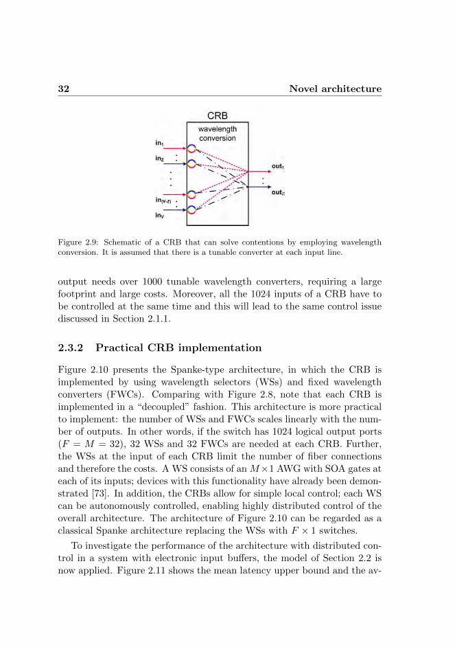
Figure 2.10 presents the Spanke-type architecture, in which the CRB isimplemented by using wavelength selectors (WSs) and fixed wavelengthconverters (FWCs). Comparing with Figure 2.8, note that each CRB isimplemented in a “decoupled” fashion. This architecture is more practicalto implement: the number of WSs and FWCs scales linearly with the num-ber of outputs. In other words, if the switch has 1024 logical output ports(F = M = 32), 32 WSs and 32 FWCs are needed at each CRB. Further,the WSs at the input of each CRB limit the number of fiber connectionsand therefore the costs. A WS consists of an M×1 AWG with SOA gates ateach of its inputs; devices with this functionality have already been demon-strated [73]. In addition, the CRBs allow for simple local control; each WScan be autonomously controlled, enabling highly distributed control of theoverall architecture. The architecture of Figure 2.10 can be regarded as aclassical Spanke architecture replacing the WSs with F × 1 switches.
To investigate the performance of the architecture with distributed con-trol in a system with electronic input buffers, the model of Section 2.2 isnow applied. Figure 2.11 shows the mean latency upper bound and the av-
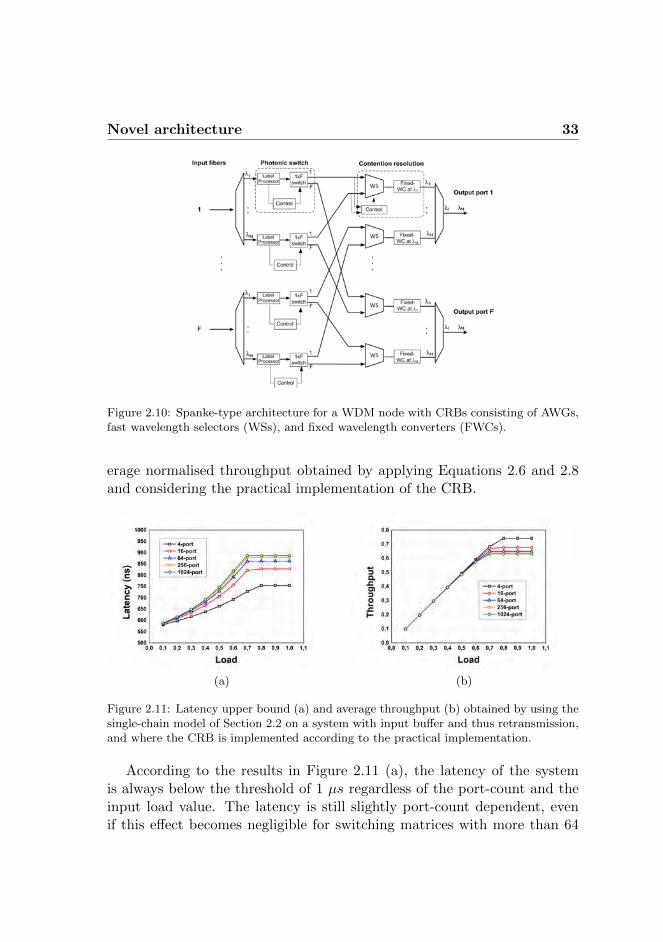
Novel architecture 33
Figure 2.10: Spanke-type architecture for a WDM node with CRBs consisting of AWGs,fast wavelength selectors (WSs), and fixed wavelength converters (FWCs).
erage normalised throughput obtained by applying Equations 2.6 and 2.8and considering the practical implementation of the CRB.
(a) (b)
Figure 2.11: Latency upper bound (a) and average throughput (b) obtained by using thesingle-chain model of Section 2.2 on a system with input buffer and thus retransmission,and where the CRB is implemented according to the practical implementation.
According to the results in Figure 2.11 (a), the latency of the systemis always below the threshold of 1 µs regardless of the port-count and theinput load value. The latency is still slightly port-count dependent, evenif this effect becomes negligible for switching matrices with more than 64
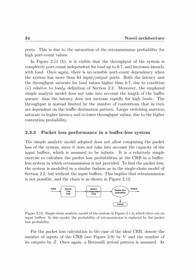
34 Novel architecture
ports. This is due to the saturation of the retransmission probability forhigh port-count values.
In Figure 2.11 (b), it is visible that the throughput of the system iscompletely port-count independent for load up to 0.7, and increases linearlywith load. Once again, there is no sensible port-count dependency whenthe system has more than 64 input/output ports. Both the latency andthe throughput saturate for load values higher than 0.7, due to condition(ii) relative to loadR definition of Section 2.2. Moreover, the employedsimple analytic model does not take into account the length of the bufferqueues: thus the latency does not increase rapidly for high loads. Thethroughput is instead limited by the number of contentions that in turnare dependent on the traffic destination pattern. Larger switching matricessaturate to higher latency and to lower throughput values, due to the highercontention probability.
2.3.3 Packet loss performance in a buffer-less system
The simple analytic model adopted does not allow computing the packetloss of the system, since it does not take into account the capacity of theinput buffers, which is assumed to be infinite. It is a relatively simpleexercise to calculate the packet loss probabilities at the CRB in a buffer-less system in which retransmission is not provided. To find the packet loss,the system is modelled in a similar fashion as in the single-chain model ofSection 2.2, but without the input buffers. This implies that retransmissionis not possible, and the chain is as shown in Figure 2.12.
Figure 2.12: Single-chain analytic model of the system in Figure 2.1 in which there are noinput buffers. In this model, the probability of retransmission is replaced by the packetloss probability.
For the packet loss calculation in the case of the ideal CRB, denote thenumber of inputs of the CRB (see Figure 2.9) by V and the number ofits outputs by Z. Once again, a Bernoulli arrival pattern is assumed. At
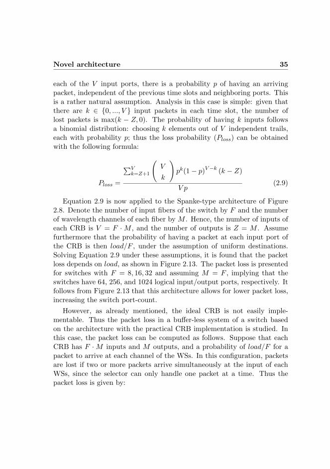
Novel architecture 35
each of the V input ports, there is a probability p of having an arrivingpacket, independent of the previous time slots and neighboring ports. Thisis a rather natural assumption. Analysis in this case is simple: given thatthere are k ∈ {0, ..., V } input packets in each time slot, the number oflost packets is max(k − Z, 0). The probability of having k inputs followsa binomial distribution: choosing k elements out of V independent trails,each with probability p; thus the loss probability (Ploss) can be obtainedwith the following formula:
Ploss =
∑Vk=Z+1
(V
k
)pk(1− p)V−k (k − Z)
V p(2.9)
Equation 2.9 is now applied to the Spanke-type architecture of Figure2.8. Denote the number of input fibers of the switch by F and the numberof wavelength channels of each fiber by M . Hence, the number of inputs ofeach CRB is V = F ·M , and the number of outputs is Z = M . Assumefurthermore that the probability of having a packet at each input port ofthe CRB is then load/F , under the assumption of uniform destinations.Solving Equation 2.9 under these assumptions, it is found that the packetloss depends on load, as shown in Figure 2.13. The packet loss is presentedfor switches with F = 8, 16, 32 and assuming M = F , implying that theswitches have 64, 256, and 1024 logical input/output ports, respectively. Itfollows from Figure 2.13 that this architecture allows for lower packet loss,increasing the switch port-count.
However, as already mentioned, the ideal CRB is not easily imple-mentable. Thus the packet loss in a buffer-less system of a switch basedon the architecture with the practical CRB implementation is studied. Inthis case, the packet loss can be computed as follows. Suppose that eachCRB has F ·M inputs and M outputs, and a probability of load/F for apacket to arrive at each channel of the WSs. In this configuration, packetsare lost if two or more packets arrive simultaneously at the input of eachWSs, since the selector can only handle one packet at a time. Thus thepacket loss is given by:
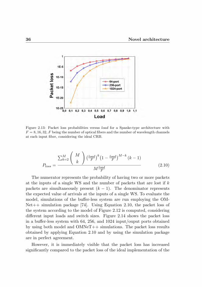
36 Novel architecture
Figure 2.13: Packet loss probabilities versus load for a Spanke-type architecture withF = 8, 16, 32, F being the number of optical fibers and the number of wavelength channelsat each input fiber, considering the ideal CRB.
Ploss =
∑Mk=2
(M
k
)(loadF
)k(1− load
F
)M−k(k − 1)
M loadF
(2.10)
The numerator represents the probability of having two or more packetsat the inputs of a single WS and the number of packets that are lost if kpackets are simultaneously present (k − 1). The denominator representsthe expected value of arrivals at the inputs of a single WS. To evaluate themodel, simulations of the buffer-less system are run employing the OM-Net++ simulation package [74]. Using Equation 2.10, the packet loss ofthe system according to the model of Figure 2.12 is computed, consideringdifferent input loads and switch sizes. Figure 2.14 shows the packet lossin a buffer-less system with 64, 256, and 1024 input/ouput ports obtainedby using both model and OMNeT++ simulations. The packet loss resultsobtained by applying Equation 2.10 and by using the simulation packageare in perfect agreement.
However, it is immediately visible that the packet loss has increasedsignificantly compared to the packet loss of the ideal implementation of the
Novel architecture 37
Figure 2.14: Packet loss probabilities versus load for a Spanke-type architecture withF = 8, 16, 32, F being the number of optical fibers and the number of wavelength channelsat each input fiber, considering the practical CRB.
CRB shown in Figure 2.13. This degradation of the performance is theprice paid for the simplicity of the CRB implementation of Figure 2.10.Note also that there is a small increment in the packet loss if the numberof ports increases.
The packet loss expressed in Equation 2.10 may be used as a rough mea-sure of the packet loss for the purpose of system and network design. In thisrespect, the architecture of Figure 2.10 can be considered as “worst case”architecture in terms of packet loss. This is sensible, since it is very thriftyin component usage and control requirements. Adding more componentsin a smart manner should only improve on Equation 2.10.
Figure 2.13 and 2.14 show the best-case scenario and worst-case scenariofor a packet loss in a WDM Spanke-type architecture with a CRB basedon wavelength conversion in a buffer-less system.
However, to understand the performance of such architecture in a real-istic environment, the system has to be simulated considering buffers witha finite capacity. This is done in the next chapter of this thesis.
38 Summary
2.4 Summary
The challenges that have to be faced in the realization of an OPS archi-tecture that could provide high port-count (> 1000), high communicationbandwidth and extremely low latency (< 1 µs) are presented.
A simple single-chain model that allows computing latency and through-put of a system as function of the particular architecture employed is in-troduced. The model is employed as a tool to show to the reader that OPSarchitectures that employ a centralized control are not suited to realize alarge port-count OPS, due to the high latency introduced by the switchreconfiguration time.
As a consequence of the results obtained using the model, a novel WDMmodular OPS architecture is presented. The proposed OPS is based on aSpanke-like architecture which employs WDM and wavelength conversionfor contention resolution purposes. The architecture is based on indepen-dent optical modules that allow highly distributed and local control. Idealand practical implementations of the contention resolution functionality arereported in combination with their performance, in terms of packet loss, ina buffer-less system. On the one hand, the ideal implementation allows forextremely low packet loss, while the practical implementation performancesdo not look promising. On the other hand, the realization of the ideal imple-mentation is cumbersome due to the high number of components requiredand to the control complexity of its contention resolution stage, while thepractical implementation is easier to realize. In this case the number ofcomponents scales linearly with the port-count and the contention resolu-tion functionality is realized in a “decoupled” manner, allowing distributedcontrol also at this stage.
To evaluate the capabilities of the OPS architecture which employs thepractical implementation of the contention resolution functionality, inputbuffers with finite capacity have to be considered.
Chapter 3
Performance investigation
In this chapter1, the performances of the proposed optical packet switch(OPS) architecture are investigated by means of simulations. Results oflatency, throughput and packet loss are presented as function of systemload in a simulated intra-DC environment. Synchronous and asynchronousoperations are taken into account as well as different traffic patterns. Buffersizing is studied in systems with fixed and variable packet lengths.
3.1 Simulation environment
The performance of the OPS architecture described in the previous chapteris studied by means of node simulations. OMNeT++ simulation package[74] is the software employed to simulate the studied DC environment.
OMNeT++ is a discrete event simulation environment commonly used
1Based on the results published in: S. Di Lucente, N. Calabretta, J.A.C. Resing,and H.J.S Dorren, “Scaling low-latency optical packet switches to a thousand ports”,IEEE/OSA Journal of Optical Communication and Networking, vol. 4, no. 9, pp. A17-A28, 2012. [61]; S. Di Lucente, R. Pueyo Centelles, H.J.S Dorren, and N. Calabretta,“Study of the performance of an optical packet switch architecture with highly distributedcontrol in a data center environment”, in Proc. of the 16th International Conference onOptical Network Design and Modeling (ONDM), Colchester, UK, 17-20, April, 2012,Page 1-6. [75]; N. Calabretta, R. Pueyo Centelles, S. Di Lucente, and H.J.S Dorren, “Onthe Performance of a Large-Scale Optical Packet Switch Under Realistic Data CenterTraffic”, IEEE/OSA Journal of Optical Communication and Networking, vol. 5, no. 6,pp. 565-573, 2013. [76]
40 Simulation environment
to simulate communication networks. This software tool provides C++ de-fined components and models. Components and models are then assembledinto larger components and models using high-level language.
The schematic of the simulated system is shown in Figure 3.1. It isan inter-cluster communication network in which the total number of in-put/output ports is F ·M . F represents the number of input optical fibersof the OPS, and thus a cluster, while M represents the number of wave-length channels carried by each fiber (λ1 to λM ). Each cluster groups Mtop-of-the-rack (TOR) switches. Each of the M TOR switches has a de-dicated queue (Queue1 to QueueM) in the F electronic input buffers asshown in the figure. Each cluster is connected to the OPS architecture byoptical fibers. Thus packets present in each queue are electrical to opticalconverted by using commercial WDM optical transceivers. A host-switchdistance of 50 meters is considered in the simulations. Longer or shorterdistances would not affect the OPS performance, but the distance betweenswitch and clusters can be regarded as a latency offset introduced in theOPS operation. The system is set to operate at a data rate of 40Gb/s, in ac-cordance with the future DC inter-cluster communication requirements [8].The OPS processes in parallel the F ·M inputs ports by using parallel 1×Fswitches, each of them autonomously controlled. The contention resolutionblock consists of M × 1 wavelength selectors (WSs), also locally controlled,and fixed wavelength converters (FWCs).
It is important to notice that possible contentions between packets com-ing from different clusters are avoided by the FWCs at the outputs of theWSs as described in Section 2.3. The FWCs convert the packet selectedby the WSs to a fixed wavelength and solve these contentions. For thisreason, only M inputs/outputs relative to a single input buffer are consid-ered, without compromising the results of the simulations. The subsystemconsidered is highlighted in Figure 3.1. Contentions occur only betweenpackets at the M inputs of each M × 1 WS.
The optical packets consist of a payload, which carries the real dataand an optical label that provides the packet destination port. In the OPSlabels are separated from the payload and processed by label processors.The label processors then control the 1×F optical switches to forward thepackets to the appropriate contention resolution block (CRB). At each CRBcontentions are avoided by the local control that selects only one packet outof the possible M incoming packets. The selected packet is forwarded to the
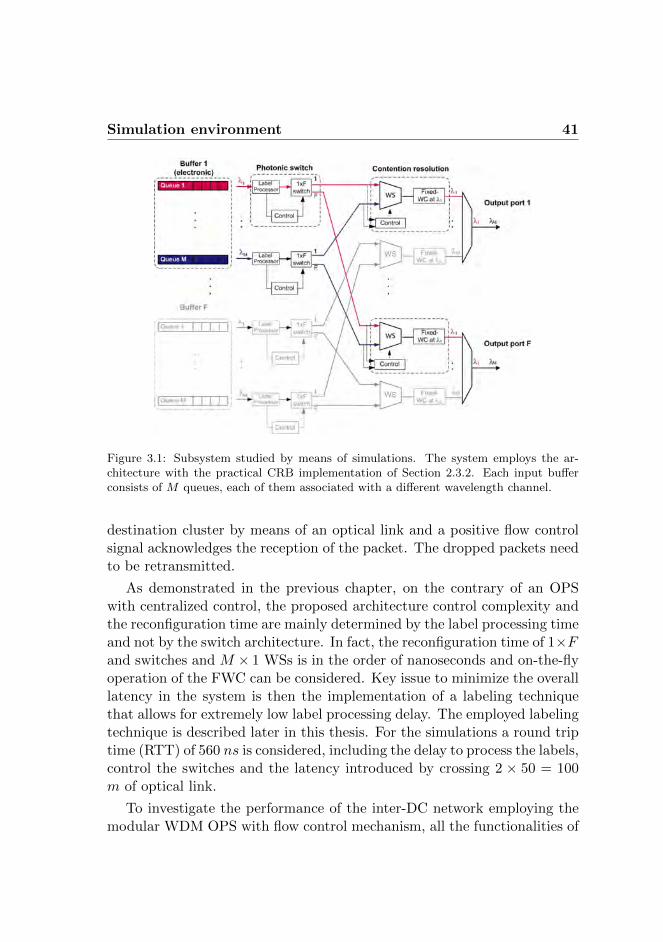
Simulation environment 41
Figure 3.1: Subsystem studied by means of simulations. The system employs the ar-chitecture with the practical CRB implementation of Section 2.3.2. Each input bufferconsists of M queues, each of them associated with a different wavelength channel.
destination cluster by means of an optical link and a positive flow controlsignal acknowledges the reception of the packet. The dropped packets needto be retransmitted.
As demonstrated in the previous chapter, on the contrary of an OPSwith centralized control, the proposed architecture control complexity andthe reconfiguration time are mainly determined by the label processing timeand not by the switch architecture. In fact, the reconfiguration time of 1×Fand switches and M × 1 WSs is in the order of nanoseconds and on-the-flyoperation of the FWC can be considered. Key issue to minimize the overalllatency in the system is then the implementation of a labeling techniquethat allows for extremely low label processing delay. The employed labelingtechnique is described later in this thesis. For the simulations a round triptime (RTT) of 560 ns is considered, including the delay to process the labels,control the switches and the latency introduced by crossing 2 × 50 = 100m of optical link.
To investigate the performance of the inter-DC network employing themodular WDM OPS with flow control mechanism, all the functionalities of
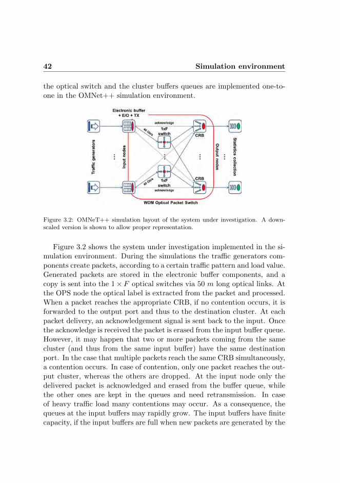
42 Simulation environment
the optical switch and the cluster buffers queues are implemented one-to-one in the OMNet++ simulation environment.
Figure 3.2: OMNeT++ simulation layout of the system under investigation. A down-scaled version is shown to allow proper representation.
Figure 3.2 shows the system under investigation implemented in the si-mulation environment. During the simulations the traffic generators com-ponents create packets, according to a certain traffic pattern and load value.Generated packets are stored in the electronic buffer components, and acopy is sent into the 1× F optical switches via 50 m long optical links. Atthe OPS node the optical label is extracted from the packet and processed.When a packet reaches the appropriate CRB, if no contention occurs, it isforwarded to the output port and thus to the destination cluster. At eachpacket delivery, an acknowledgement signal is sent back to the input. Oncethe acknowledge is received the packet is erased from the input buffer queue.However, it may happen that two or more packets coming from the samecluster (and thus from the same input buffer) have the same destinationport. In the case that multiple packets reach the same CRB simultaneously,a contention occurs. In case of contention, only one packet reaches the out-put cluster, whereas the others are dropped. At the input node only thedelivered packet is acknowledged and erased from the buffer queue, whilethe other ones are kept in the queues and need retransmission. In caseof heavy traffic load many contentions may occur. As a consequence, thequeues at the input buffers may rapidly grow. The input buffers have finitecapacity, if the input buffers are full when new packets are generated by the
Synchronous operation 43
traffic generators, they are considered lost and used to calculate the packetloss ratio.
3.2 Synchronous operation
At the first stage of the OPS architecture performance evaluation, the OM-NeT++ implementation of the subsystem highlighted in Figure 3.1 is setto operate in discrete time. During the simulation runs the operations aretime slotted and the system operates as follows.
At each time slot, each traffic generator creates packets according toa binomial distribution with fixed priority (hereafter called load). Thus,there is probability load of having a new packet at each queue of the inputbuffer considered. All traffic generators are programmed to operate inde-pendently, but with the same load. As a consequence, the load set at thebeginning of the simulation represents the mean load value in the system,while the current load may vary from 0 to 1 in each time slot studied dur-ing the simulation run. Packets destinations are chosen randomly betweenall possible outputs according to a uniform distribution. Packet durationis set to be of 40 ns (200 bytes, considering that the system operates ata data rate of 40 Gb/s). A copy of the first packets in each of the bufferqueues is sent to the 1×F switches. At this stage, after RTT/2, the packetslabels are read and the packets payloads are forwarded to the appropriateCRB. After RTT, a positive or negative acknowledgement message for eachpacket is received back at the transmitting inputs. In case of positive ac-knowledgment, the corresponding packet is erased from the buffer queue. Incase of negative acknowledgment, another copy of the corresponding packetis transmitted to the OPS. In order to have uniform queues at the inputbuffers, in case of output contentions, the CRB are programmed to employa round robin algorithm to select the contention winner. Thus packet prior-ity is a priori determined, uniformly distributed between the packets of thedifferent queues and no extra latency is added to the system. Input bufferqueues have a capacity of 14 packets, according to the rule of thumb thatsays that the amount of required buffering B is B = RTT × PacketRate(B = 560 [ns]× 1/40 [packets/ns] = 14 [packets]). Depending on the traf-fic load considered and the number of contentions, it may happen that abuffer queue is already full when a new packet is generated by the traffic
44 Synchronous operation
generators. In this scenario, the new packet is immediately dropped andlost, due to buffer overflowing.
The simulations are run under different values of mean load and fordifferent switch sizes. To facilitate the discussion, the number of input fiberF is set equal to the number of wavelength channels carried by each fiberM . Similar results, not reported, can be obtained for M > F , consideringthat each WS could select more WDM channels at the same time in thiscase. With M < F , the architecture implementation requires an extra stageof WSs at each CRB. In this case, the number of M × 1 WSs in each CRBis equal to the number of input fibers F . F is also the number of outputsdirected to the FWCs, but only M < F wavelength channels are availableat each output fiber of the OPS. An extra stage of WSs is needed to reducethe number of outputs directed to the FWCs down to M . However, thiscase is negligible since hundreds of WDM channels can be transported by asingle fiber, increasing the system spectral efficiency. The acknowledgementmessages are not considered in the system traffic and the lost packets arenot considered in the calculation of the average latency that the packetsexperience in the system. At the output of the system the transmittedpackets are collected to calculate the average latency they experience inthe system and to compute the system throughput. As already mentioned,lost packets are considered to compute the packet loss ratio.
Figures 3.3 (a), (b) and (c) show the average latency, the packet lossand the throughput of the system, respectively. The simulations are runfor 1010 time slots. The performances of switches with 4, 16, 64, 256 and1024 input/output ports are investigated, assuming F = M = 2, 4, 8, 16and 32.
In Figure 3.3 (a), it is visible that the system latency increases with thenumber of ports. However, the increment becomes smaller and smaller andan asymptotic curve is rapidly reached. In the same figure is also visiblethat the latency increases linearly with the load until load values around0.7. After this threshold the latency rapidly increases. This behavior canbe explained as follows: on the one hand higher load leads to the pres-ence of more packets in the system and thus higher number of contentions.Having more contentions implies higher probability for a packet to be re-transmitted and thus increased latency. On the other hand over the 0.7threshold of the load, buffer overflowing is unavoidable. In this scenario,many packets are dropped and others have to be re-transmitted several
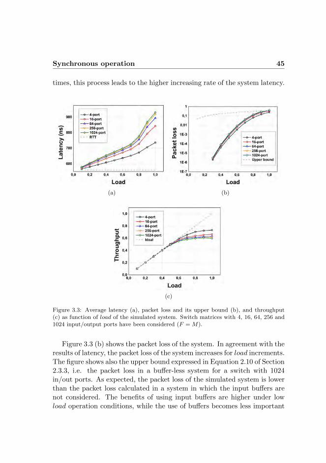
Synchronous operation 45
times, this process leads to the higher increasing rate of the system latency.
(a) (b)
(c)
Figure 3.3: Average latency (a), packet loss and its upper bound (b), and throughput(c) as function of load of the simulated system. Switch matrices with 4, 16, 64, 256 and1024 input/output ports have been considered (F = M).
Figure 3.3 (b) shows the packet loss of the system. In agreement with theresults of latency, the packet loss of the system increases for load increments.The figure shows also the upper bound expressed in Equation 2.10 of Section2.3.3, i.e. the packet loss in a buffer-less system for a switch with 1024in/out ports. As expected, the packet loss of the simulated system is lowerthan the packet loss calculated in a system in which the input buffers arenot considered. The benefits of using input buffers are higher under lowload operation conditions, while the use of buffers becomes less important
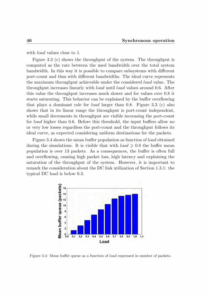
46 Synchronous operation
with load values close to 1.
Figure 3.3 (c) shows the throughput of the system. The throughput iscomputed as the rate between the used bandwidth over the total systembandwidth. In this way it is possible to compare subsystems with differentport-count and thus with different bandwidths. The ideal curve representsthe maximum throughput achievable under the considered load value. Thethroughput increases linearly with load until load values around 0.6. Afterthis value the throughput increases much slower and for values over 0.8 itstarts saturating. This behavior can be explained by the buffer overflowingthat plays a dominant role for load larger than 0.8. Figure 3.3 (c) alsoshows that in its linear range the throughput is port-count independent,while small decrements in throughput are visible increasing the port-countfor load higher than 0.6. Before this threshold, the input buffers allow noor very low losses regardless the port-count and the throughput follows itsideal curve, as expected considering uniform destinations for the packets.
Figure 3.4 shows the mean buffer population as function of load obtainedduring the simulations. It is visible that with load > 0.8 the buffer meanpopulation is over 13 packets. As a consequences, the buffer is often fulland overflowing, causing high packet loss, high latency and explaining thesaturation of the throughput of the system. However, it is important toremark the consideration about the DC link utilization of Section 1.3.1: thetypical DC load is below 0.3.
Figure 3.4: Mean buffer queue as a function of load expressed in number of packets.
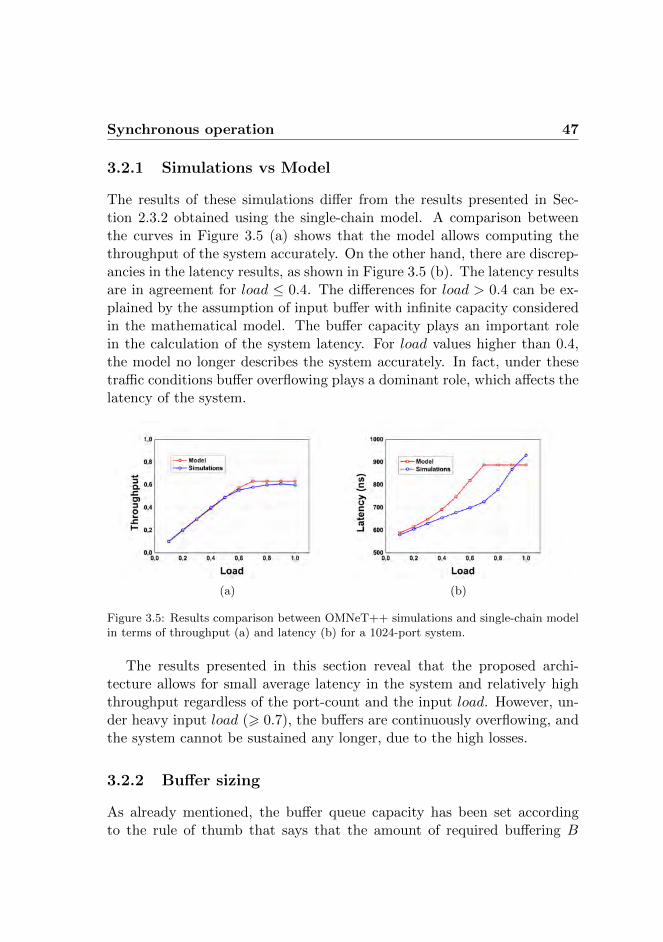
Synchronous operation 47
3.2.1 Simulations vs Model
The results of these simulations differ from the results presented in Sec-tion 2.3.2 obtained using the single-chain model. A comparison betweenthe curves in Figure 3.5 (a) shows that the model allows computing thethroughput of the system accurately. On the other hand, there are discrep-ancies in the latency results, as shown in Figure 3.5 (b). The latency resultsare in agreement for load ≤ 0.4. The differences for load > 0.4 can be ex-plained by the assumption of input buffer with infinite capacity consideredin the mathematical model. The buffer capacity plays an important rolein the calculation of the system latency. For load values higher than 0.4,the model no longer describes the system accurately. In fact, under thesetraffic conditions buffer overflowing plays a dominant role, which affects thelatency of the system.
(a) (b)
Figure 3.5: Results comparison between OMNeT++ simulations and single-chain modelin terms of throughput (a) and latency (b) for a 1024-port system.
The results presented in this section reveal that the proposed archi-tecture allows for small average latency in the system and relatively highthroughput regardless of the port-count and the input load. However, un-der heavy input load (> 0.7), the buffers are continuously overflowing, andthe system cannot be sustained any longer, due to the high losses.
3.2.2 Buffer sizing
As already mentioned, the buffer queue capacity has been set accordingto the rule of thumb that says that the amount of required buffering B
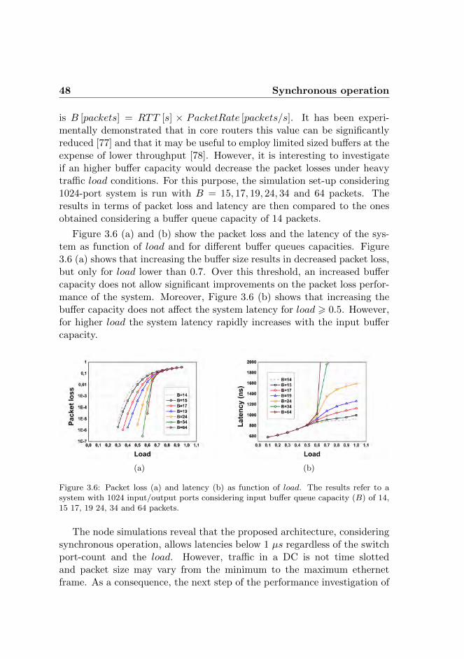
48 Synchronous operation
is B [packets] = RTT [s] × PacketRate [packets/s]. It has been experi-mentally demonstrated that in core routers this value can be significantlyreduced [77] and that it may be useful to employ limited sized buffers at theexpense of lower throughput [78]. However, it is interesting to investigateif an higher buffer capacity would decrease the packet losses under heavytraffic load conditions. For this purpose, the simulation set-up considering1024-port system is run with B = 15, 17, 19, 24, 34 and 64 packets. Theresults in terms of packet loss and latency are then compared to the onesobtained considering a buffer queue capacity of 14 packets.
Figure 3.6 (a) and (b) show the packet loss and the latency of the sys-tem as function of load and for different buffer queues capacities. Figure3.6 (a) shows that increasing the buffer size results in decreased packet loss,but only for load lower than 0.7. Over this threshold, an increased buffercapacity does not allow significant improvements on the packet loss perfor-mance of the system. Moreover, Figure 3.6 (b) shows that increasing thebuffer capacity does not affect the system latency for load > 0.5. However,for higher load the system latency rapidly increases with the input buffercapacity.
(a) (b)
Figure 3.6: Packet loss (a) and latency (b) as function of load. The results refer to asystem with 1024 input/output ports considering input buffer queue capacity (B) of 14,15 17, 19 24, 34 and 64 packets.
The node simulations reveal that the proposed architecture, consideringsynchronous operation, allows latencies below 1 µs regardless of the switchport-count and the load. However, traffic in a DC is not time slottedand packet size may vary from the minimum to the maximum ethernetframe. As a consequence, the next step of the performance investigation of
Asynchronous operation 49
the OPS architecture studied is to simulate a system considering a trafficpattern that realistically represents DC traffic. This is done in the nextsection of this chapter.
3.3 Asynchronous operation
To evaluate the performance of the OPS architecture under investigation, adata center-like traffic pattern is considered. The simulation set-up remainsthe same of Figure 3.1. However, the functionalities of traffic generator andCRB OMNeT++ components are modified.
3.3.1 Self-similar traffic
During these simulations, the traffic generators are programmed to createpackets with any arbitrary length, and send them to the 1 × F switchesaccording to specific inter-arrival time parameters. Each of these compo-nents emulates the aggregated traffic of a TOR switch. Each of the Minputs of a single cluster receives the input traffic generated by 200 simu-lated servers. The amount of input load is normalized and is scaled from0 to 1. The generation of DC traffic is based on referred publications re-garding this topic [25, 26]. Moreover, data from more general studies aboutInternet traffic are also taken into account [79, 80]. According to thesepublications, packet length in a realistic DC scenario shows a bimodal dis-tribution around 40 and 1500 bytes. These values match the minimum andthe maximum Ethernet frame length, respectively. Figure 3.7 (a) and (b)show the cumulative distribution function (CDF) and the histogram of thepacket length generated by the traffic generators during the simulations.
Packet inter-arrival time is modelled matching ON/OFF periods (withand without packet retransmission). The length of these ON/OFF periodsis characterized by heavy-tailed self-similar distributions. In the simula-tion set-up studied, a Pareto distribution has been employed to model thelength of the ON/OFF periods. Figure 3.8 (a) and (b) show the ON andOFF period length CDFs. ON periods follow the same length distributionregardless of the chosen traffic load value. However, the time between them(i.e. the OFF period) is inversely proportional to load. When a higher loadis selected they become shorter and vice versa. As a consequence, the traf-

50 Asynchronous operation
(a)
(b)
Figure 3.7: Cumulative distribution function (CDF) (a) and histogram (b) of the gener-ated packets length.
fic complexity remains constant regardless the chosen load, while it is thetraffic density that varies in simulations with different load values.
Flattening the DC network architecture at cluster level allows to assumethat the communication performances in the system do not depend on thedistance or hierarchical position of the destination nodes. In addition, itis assumed that the traffic in the system is equally spread through all theresources. This is a natural assumption considering the aggregated trafficof hundreds of servers at cluster level instead of the traffic at server level. Inother words, during the simulation, all packets in every transmission (ONperiods) are randomly sent with uniform distribution to one of the possibledestinations.
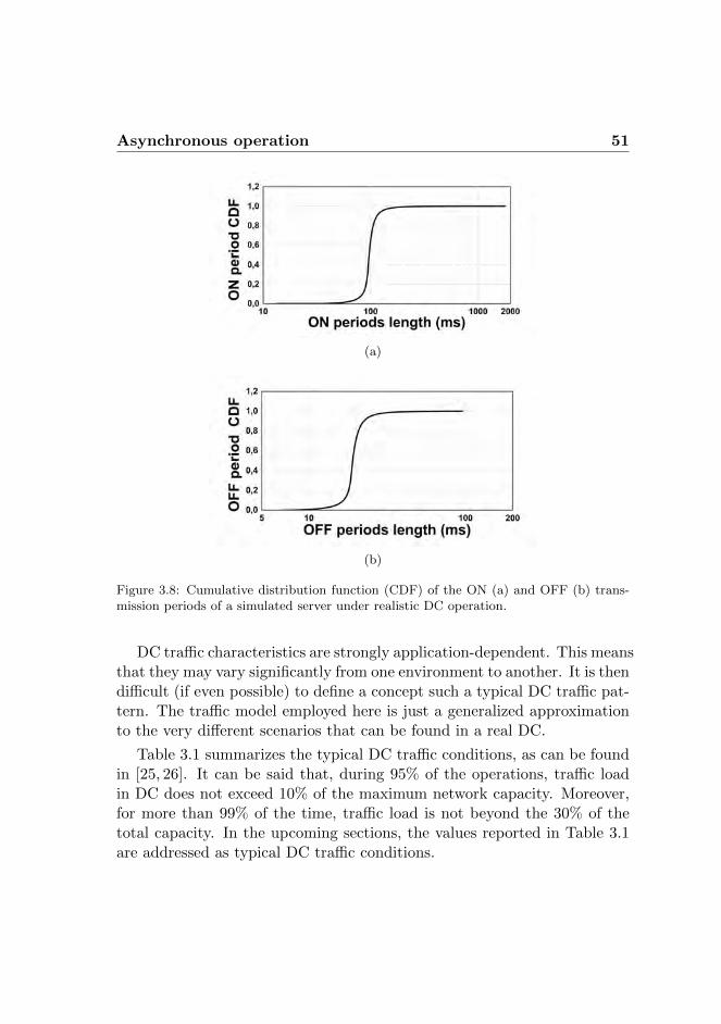
Asynchronous operation 51
(a)
(b)
Figure 3.8: Cumulative distribution function (CDF) of the ON (a) and OFF (b) trans-mission periods of a simulated server under realistic DC operation.
DC traffic characteristics are strongly application-dependent. This meansthat they may vary significantly from one environment to another. It is thendifficult (if even possible) to define a concept such a typical DC traffic pat-tern. The traffic model employed here is just a generalized approximationto the very different scenarios that can be found in a real DC.
Table 3.1 summarizes the typical DC traffic conditions, as can be foundin [25, 26]. It can be said that, during 95% of the operations, traffic loadin DC does not exceed 10% of the maximum network capacity. Moreover,for more than 99% of the time, traffic load is not beyond the 30% of thetotal capacity. In the upcoming sections, the values reported in Table 3.1are addressed as typical DC traffic conditions.
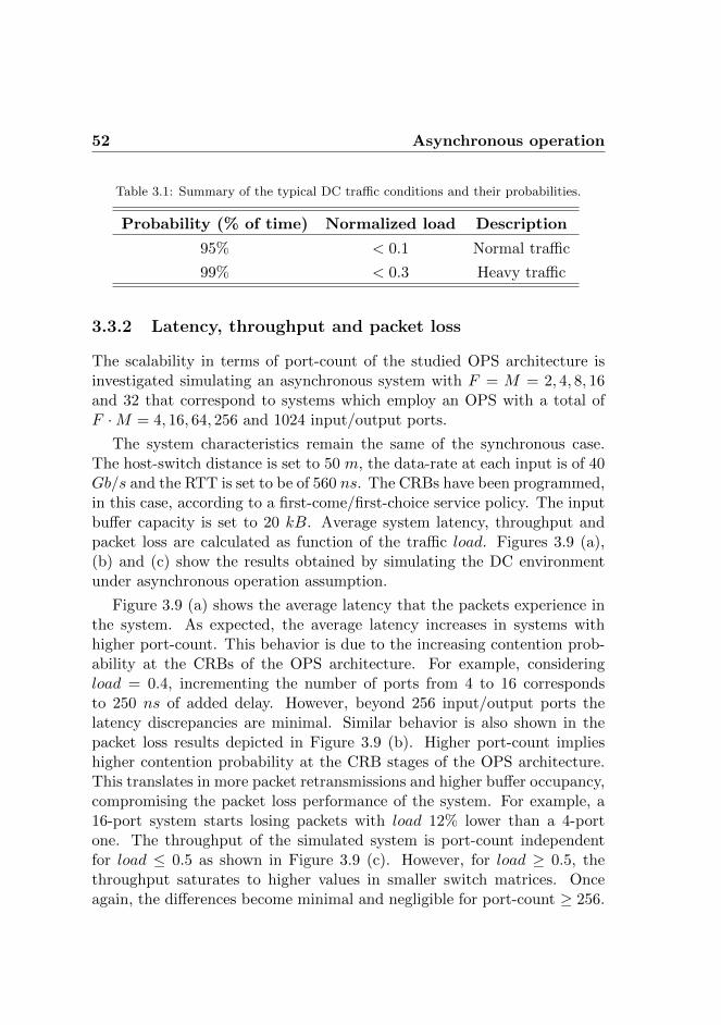
52 Asynchronous operation
Table 3.1: Summary of the typical DC traffic conditions and their probabilities.
Probability (% of time) Normalized load Description
95% < 0.1 Normal traffic
99% < 0.3 Heavy traffic
3.3.2 Latency, throughput and packet loss
The scalability in terms of port-count of the studied OPS architecture isinvestigated simulating an asynchronous system with F = M = 2, 4, 8, 16and 32 that correspond to systems which employ an OPS with a total ofF ·M = 4, 16, 64, 256 and 1024 input/output ports.
The system characteristics remain the same of the synchronous case.The host-switch distance is set to 50 m, the data-rate at each input is of 40Gb/s and the RTT is set to be of 560 ns. The CRBs have been programmed,in this case, according to a first-come/first-choice service policy. The inputbuffer capacity is set to 20 kB. Average system latency, throughput andpacket loss are calculated as function of the traffic load. Figures 3.9 (a),(b) and (c) show the results obtained by simulating the DC environmentunder asynchronous operation assumption.
Figure 3.9 (a) shows the average latency that the packets experience inthe system. As expected, the average latency increases in systems withhigher port-count. This behavior is due to the increasing contention prob-ability at the CRBs of the OPS architecture. For example, consideringload = 0.4, incrementing the number of ports from 4 to 16 correspondsto 250 ns of added delay. However, beyond 256 input/output ports thelatency discrepancies are minimal. Similar behavior is also shown in thepacket loss results depicted in Figure 3.9 (b). Higher port-count implieshigher contention probability at the CRB stages of the OPS architecture.This translates in more packet retransmissions and higher buffer occupancy,compromising the packet loss performance of the system. For example, a16-port system starts losing packets with load 12% lower than a 4-portone. The throughput of the simulated system is port-count independentfor load ≤ 0.5 as shown in Figure 3.9 (c). However, for load ≥ 0.5, thethroughput saturates to higher values in smaller switch matrices. Onceagain, the differences become minimal and negligible for port-count ≥ 256.
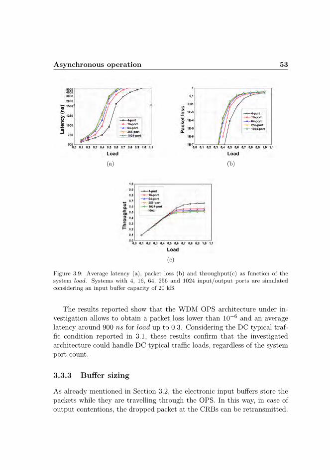
Asynchronous operation 53
(a) (b)
(c)
Figure 3.9: Average latency (a), packet loss (b) and throughput(c) as function of thesystem load. Systems with 4, 16, 64, 256 and 1024 input/output ports are simulatedconsidering an input buffer capacity of 20 kB.
The results reported show that the WDM OPS architecture under in-vestigation allows to obtain a packet loss lower than 10−6 and an averagelatency around 900 ns for load up to 0.3. Considering the DC typical traf-fic condition reported in 3.1, these results confirm that the investigatedarchitecture could handle DC typical traffic loads, regardless of the systemport-count.
3.3.3 Buffer sizing
As already mentioned in Section 3.2, the electronic input buffers store thepackets while they are travelling through the OPS. In this way, in case ofoutput contentions, the dropped packet at the CRBs can be retransmitted.
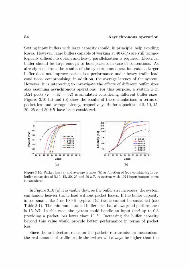
54 Asynchronous operation
Setting input buffers with large capacity should, in principle, help avoidinglosses. However, large buffers capable of working at 40 Gb/s are still techno-logically difficult to obtain and heavy parallelization is required. Electricalbuffer should be large enough to hold packets in case of contentions. Asalready seen from the results of the synchronous operation case, a largerbuffer does not improve packet loss performance under heavy traffic loadconditions, compromising, in addition, the average latency of the system.However, it is interesting to investigate the effects of different buffer sizesalso assuming asynchronous operations. For this purpose, a system with1024 ports (F = M = 32) is simulated considering different buffer sizes.Figures 3.10 (a) and (b) show the results of these simulations in terms ofpacket loss and average latency, respectively. Buffer capacities of 5, 10, 15,20, 25 and 50 kB have been considered.
(a) (b)
Figure 3.10: Packet loss (a) and average latency (b) as function of load considering inputbuffer capacities of 5,10, 15, 20, 25 and 50 kB. A system with 1024 input/output portsis considered.
In Figure 3.10 (a) it is visible that, as the buffer size increases, the systemcan handle heavier traffic load without packet losses. If the buffer capacityis too small, like 5 or 10 kB, typical DC traffic cannot be sustained (seeTable 3.1). The minimum studied buffer size that allows good performanceis 15 kB. In this case, the system could handle an input load up to 0.3providing a packet loss lower than 10−6. Increasing the buffer capacitybeyond this value would provide better performance in terms of packetloss.
Since the architecture relies on the packets retransmission mechanism,the real amount of traffic inside the switch will always be higher than the
Discussion 55
input traffic. For this reason, even a very large size buffer, would not achievelossless operation considering load ≥ 0.7. Beyond this load value packetloss is buffer capacity independent.
The buffer capacity affects also the average system latency: if more pack-ets can be held in the queues, they will end up waiting a longer time beforebeing transmitted. Figure 3.10 (b) shows the effect of having different buffercapacity on the average system latency. According to those results, a bufferof 20 kB should be enough to assure a packet loss below 10−6 for typicalDC traffic and up to load = 0.35 providing sub-microsecond latencies ( ∼900 ns ). This is the reason why 20 kB has been intentionally used in theprevious section to investigate the performance of different sized systems.Higher buffer capacity could be considered to extend lossless operation tohigher load. For example, with 50 kB buffer per port, the system couldhandle load ≤ 0.45. However, the trade-off between packet loss and latencyimplies that the packets would suffer on average a latency higher than 2µs. In a real environment, an optimal buffer capacity should be chosendepending on the application requirements.
3.4 Discussion
The performances of the proposed optical packet switch architecture imple-mentation in terms of latency, throughput and packet loss are investigatedby means of OMNeT++ simulations. Two different traffic pattern andsystem operations are considered. In the time slotted case, fixed size pack-ets are generated according to a binomial distribution. In the asynchronouscase, packets with a variable length are generated according to a self-similardistribution with inter arrival time based on the Pareto distribution. Inboth cases, uniform distributed destinations are considered.
Synchronous vs Asynchronous simulations
As expected, the performance results in terms of latency and throughputobtained assuming asynchronous operation of the system are worse thanthe synchronous case. This is due to the fact that the probability of con-tention is higher in a system in which the packets can be transmitted atany arbitrary time and in which the packet length may considerably vary.
56 Discussion
In the latency results, that strongly depends on the number of packet con-tentions, this phenomenon is evident. In the synchronous simulations, thesystem latency is below 1 µs regardless the switch port-count and the loadvalue considered. In the asynchronous case, the latency increases rapidlywith the input load and is higher than 1 µs for load around 0.4 for all theswitch port-count considered.
The throughput results show a similar behavior in both the operationmethods considered. However, the performance slightly worsen in the asyn-chronous operation, again for the higher contention probability of the asyn-chronous system.
It is difficult to compare the packet loss results. These results are slightlydependent on the port-count of the considered system, but strongly depen-dent on the buffer capacity. The two considered cases (synchronous andasynchronous) differ for packet size, fixed and set to 200 bytes in the firstcase and variable between 40 bytes and 1500 bytes in the second case. As aconsequence, different buffer capacities have been considered, compromis-ing a possible comparison in terms of packet loss between the two systems.However, in both cases, no losses are shown for load < 0.3.
Buffer sizing
The effects of the buffer capacity on the system latency and packet loss areinvestigated for both the synchronous and asynchronous case. The resultsare very interesting. In both cases, increasing the buffer capacity does notcorrespond to a decrement of the packet loss under heavy traffic conditions(load > 0.7). An higher buffer capacity improves the system performanceonly for load values lower than this threshold. Moreover, the latency resultsreveal that the latency of the system is strongly dependent on the buffercapacity. The latency is higher in systems with larger buffers. This is dueto the longer queueing times that the packets experience in buffers with alarger capacity.
In general, buffer sizing leads to a trade-off between packet loss and sys-tem latency. In this context, the system requirements in a DC environmentare strongly application dependent. However, in all simulated operationsthe investigated OPS architecture allows providing promising results. Nopacket loss, high throughput and sub-microsecond latency can be achievedunder relatively high traffic loads (< 0.4) and employing limited input
Summary 57
buffer capacities.
3.5 Summary
The performance of the modular WDM OPS with highly distributed controlare investigated by means of node simulations. Two sets of simulations areconsidered. First, the DC inter-cluster network is assumed to operate indiscrete time. The results in terms of average latency, throughput andpacket loss, assuming synchronous operation, reveal that the investigatedOPS architecture allows for sub-microsecond latencies, while providing lowpacket loss and high throughput, regardless the system port-count.
Second, asynchronous operation and variable packets lengths are con-sidered during the simulations. The traffic pattern is modelled to describethe typical DC traffic conditions. Also in this case, results of average la-tency, throughput and packet loss as function of input load are reported.A degradation of the system performance is visible comparing these resultswith the ones obtained by considering synchronous operation. However,the OPS would be able to handle DC-like traffic providing an average la-tency around 900 ns, a packet loss lower than 10−6 and relatively highthroughput.
In both synchronous and asynchronous cases, the effects of the buffer ca-pacity on the system performance are investigated. The results are similarfor both of the simulation sets considered. On the one hand, a limited buffersize (14 packets for the synchronous case and 20 kB for the asynchronouscase) is able to guarantee lossless operation for typical DC traffic load.On the other hand, increasing buffer capacity does not help improving thepacket loss performance of the system under heavy traffic load conditions(load ≥ 0.7), compromising also the average packet latency.

Chapter 4
Dynamic switching
In this chapter1, all functionalities of the studied optical packet switch(OPS) architecture, with the only exception of the flow control mechanism,are implemented and experimentally evaluated. Labeling technique, labelprocessor, 1×F optical switch, switch controller and CRB implementationsare described in this chapter. The dynamic switching capabilities, consider-ing synchronous operation, are first investigated injecting 8 WDM channelsat 40 Gb/s into a single 1× 8 optical module. In this case, discrete switch-ing components are used to implement the 1 × 8 optical module. Resultsof the dynamic operations and bit-error-rate measurements are reported.The experiment reveals that it is feasible to realize a 64 × 64 OPS basedon the proposed architecture. The possible integration of a 16 × 16 OPSbased on the studied architecture is then investigated injecting 4 WDMoptical channels at 40 Gb/s into a 1 × 4 integrated optical cross-connect.
1Based on the results published in: J. Luo, S. Di Lucente, J. Ramirez, H.J.S. Dor-ren, and N. Calabretta, “Low Latency and Large Port Count Optical Packet Switchwith Highly Distributed Control”, in Proc. of Optical Fiber Communication/NationalFiber Optic Engineers Conference (OFC/NFOC), Los Angeles, USA, 4-8, March, 2012,Paper OW3J.2. [81]; S. Di Lucente, J. Luo, A. Rohit, S. Zou, K.A. Williams, H.J.S Dor-ren, and N. Calabretta, “FPGA Controlled Integrated Optical Cross-Connect Modulefor High Port-Density Optical Packet Switch”, in Proc. European Conference on Op-tical Communication (ECOC), Amsterdam, The Netherlands, 16-20, Sep. 2012, PaperTu.3.A.3. [82]; S. Di Lucente, R. Pueyo Centelles, J. Luo, A. Rohit, S. Zou, K.A. Wil-liams, H.J.S Dorren, and N. Calabretta, “Numerical and experimental study of a highport-density WDM optical packet switch architecture for data centers”, Optics express,vol. 21, no. 1, pp. 263-269, 2013. [83]
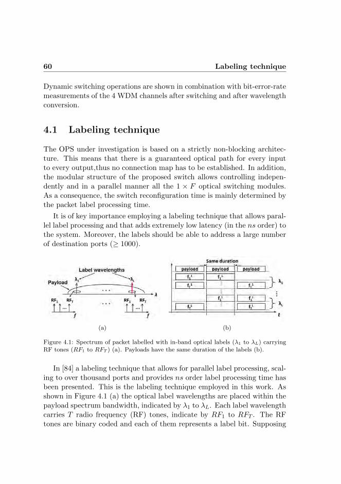
60 Labeling technique
Dynamic switching operations are shown in combination with bit-error-ratemeasurements of the 4 WDM channels after switching and after wavelengthconversion.
4.1 Labeling technique
The OPS under investigation is based on a strictly non-blocking architec-ture. This means that there is a guaranteed optical path for every inputto every output,thus no connection map has to be established. In addition,the modular structure of the proposed switch allows controlling indepen-dently and in a parallel manner all the 1 × F optical switching modules.As a consequence, the switch reconfiguration time is mainly determined bythe packet label processing time.
It is of key importance employing a labeling technique that allows paral-lel label processing and that adds extremely low latency (in the ns order) tothe system. Moreover, the labels should be able to address a large numberof destination ports (≥ 1000).
(a) (b)
Figure 4.1: Spectrum of packet labelled with in-band optical labels (λ1 to λL) carryingRF tones (RF1 to RFT ) (a). Payloads have the same duration of the labels (b).
In [84] a labeling technique that allows for parallel label processing, scal-ing to over thousand ports and provides ns order label processing time hasbeen presented. This is the labeling technique employed in this work. Asshown in Figure 4.1 (a) the optical label wavelengths are placed within thepayload spectrum bandwidth, indicated by λ1 to λL. Each label wavelengthcarries T radio frequency (RF) tones, indicate by RF1 to RFT . The RFtones are binary coded and each of them represents a label bit. Supposing
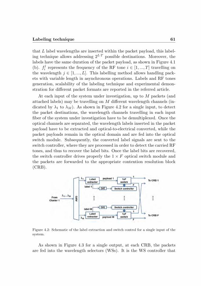
Labeling technique 61
that L label wavelengths are inserted within the packet payload, this label-ing technique allows addressing 2L·T possible destinations. Moreover, thelabels have the same duration of the packet payload, as shown in Figure 4.1(b). f ji represents the frequency of the RF tone i ∈ [1, ..., T ] travelling onthe wavelength j ∈ [1, ..., L]. This labelling method allows handling pack-ets with variable length in asynchronous operations. Labels and RF tonesgeneration, scalability of the labeling technique and experimental demon-stration for different packet formats are reported in the referred article.
At each input of the system under investigation, up to M packets (andattached labels) may be travelling on M different wavelength channels (in-dicated by λ1 to λM ). As shown in Figure 4.2 for a single input, to detectthe packet destinations, the wavelength channels travelling in each inputfiber of the system under investigation have to be demultiplexed. Once theoptical channels are separated, the wavelength labels inserted in the packetpayload have to be extracted and optical-to-electrical converted, while thepacket payloads remain in the optical domain and are fed into the opticalswitch module. Subsequently, the converted label signals are sent to theswitch controller, where they are processed in order to detect the carried RFtones, and thus to recover the label bits. Once the label bits are recovered,the switch controller drives properly the 1 × F optical switch module andthe packets are forwarded to the appropriate contention resolution block(CRB).
Figure 4.2: Schematic of the label extraction and switch control for a single input of thesystem.
As shown in Figure 4.3 for a single output, at each CRB, the packetsare fed into the wavelength selectors (WSs). It is the WS controller that
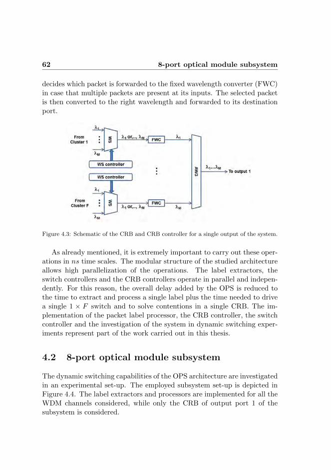
62 8-port optical module subsystem
decides which packet is forwarded to the fixed wavelength converter (FWC)in case that multiple packets are present at its inputs. The selected packetis then converted to the right wavelength and forwarded to its destinationport.
Figure 4.3: Schematic of the CRB and CRB controller for a single output of the system.
As already mentioned, it is extremely important to carry out these oper-ations in ns time scales. The modular structure of the studied architectureallows high parallelization of the operations. The label extractors, theswitch controllers and the CRB controllers operate in parallel and indepen-dently. For this reason, the overall delay added by the OPS is reduced tothe time to extract and process a single label plus the time needed to drivea single 1 × F switch and to solve contentions in a single CRB. The im-plementation of the packet label processor, the CRB controller, the switchcontroller and the investigation of the system in dynamic switching exper-iments represent part of the work carried out in this thesis.
4.2 8-port optical module subsystem
The dynamic switching capabilities of the OPS architecture are investigatedin an experimental set-up. The employed subsystem set-up is depicted inFigure 4.4. The label extractors and processors are implemented for all theWDM channels considered, while only the CRB of output port 1 of thesubsystem is considered.
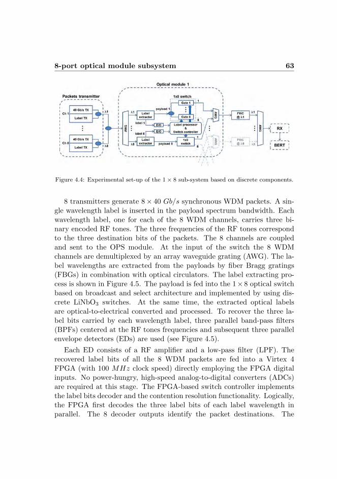
8-port optical module subsystem 63
Figure 4.4: Experimental set-up of the 1 × 8 sub-system based on discrete components.
8 transmitters generate 8× 40 Gb/s synchronous WDM packets. A sin-gle wavelength label is inserted in the payload spectrum bandwidth. Eachwavelength label, one for each of the 8 WDM channels, carries three bi-nary encoded RF tones. The three frequencies of the RF tones correspondto the three destination bits of the packets. The 8 channels are coupledand sent to the OPS module. At the input of the switch the 8 WDMchannels are demultiplexed by an array waveguide grating (AWG). The la-bel wavelengths are extracted from the payloads by fiber Bragg gratings(FBGs) in combination with optical circulators. The label extracting pro-cess is shown in Figure 4.5. The payload is fed into the 1× 8 optical switchbased on broadcast and select architecture and implemented by using dis-crete LiNbO3 switches. At the same time, the extracted optical labelsare optical-to-electrical converted and processed. To recover the three la-bel bits carried by each wavelength label, three parallel band-pass filters(BPFs) centered at the RF tones frequencies and subsequent three parallelenvelope detectors (EDs) are used (see Figure 4.5).
Each ED consists of a RF amplifier and a low-pass filter (LPF). Therecovered label bits of all the 8 WDM packets are fed into a Virtex 4FPGA (with 100 MHz clock speed) directly employing the FPGA digitalinputs. No power-hungry, high-speed analog-to-digital converters (ADCs)are required at this stage. The FPGA-based switch controller implementsthe label bits decoder and the contention resolution functionality. Logically,the FPGA first decodes the three label bits of each label wavelength inparallel. The 8 decoder outputs identify the packet destinations. The
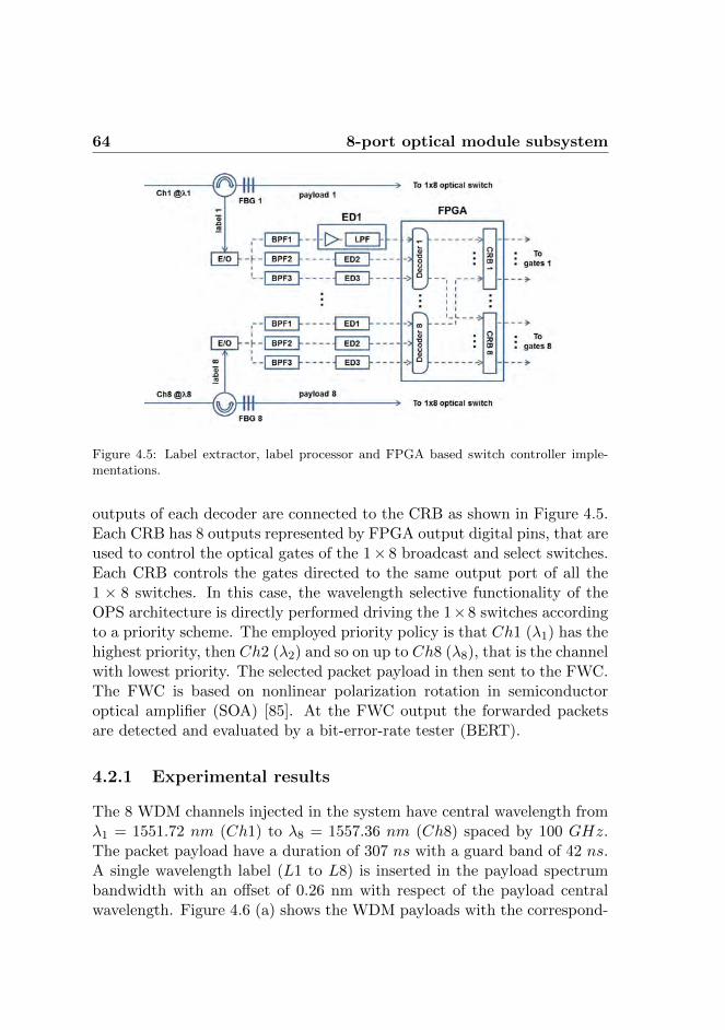
64 8-port optical module subsystem
Figure 4.5: Label extractor, label processor and FPGA based switch controller imple-mentations.
outputs of each decoder are connected to the CRB as shown in Figure 4.5.Each CRB has 8 outputs represented by FPGA output digital pins, that areused to control the optical gates of the 1× 8 broadcast and select switches.Each CRB controls the gates directed to the same output port of all the1 × 8 switches. In this case, the wavelength selective functionality of theOPS architecture is directly performed driving the 1×8 switches accordingto a priority scheme. The employed priority policy is that Ch1 (λ1) has thehighest priority, then Ch2 (λ2) and so on up to Ch8 (λ8), that is the channelwith lowest priority. The selected packet payload in then sent to the FWC.The FWC is based on nonlinear polarization rotation in semiconductoroptical amplifier (SOA) [85]. At the FWC output the forwarded packetsare detected and evaluated by a bit-error-rate tester (BERT).
4.2.1 Experimental results
The 8 WDM channels injected in the system have central wavelength fromλ1 = 1551.72 nm (Ch1) to λ8 = 1557.36 nm (Ch8) spaced by 100 GHz.The packet payload have a duration of 307 ns with a guard band of 42 ns.A single wavelength label (L1 to L8) is inserted in the payload spectrumbandwidth with an offset of 0.26 nm with respect of the payload centralwavelength. Figure 4.6 (a) shows the WDM payloads with the correspond-
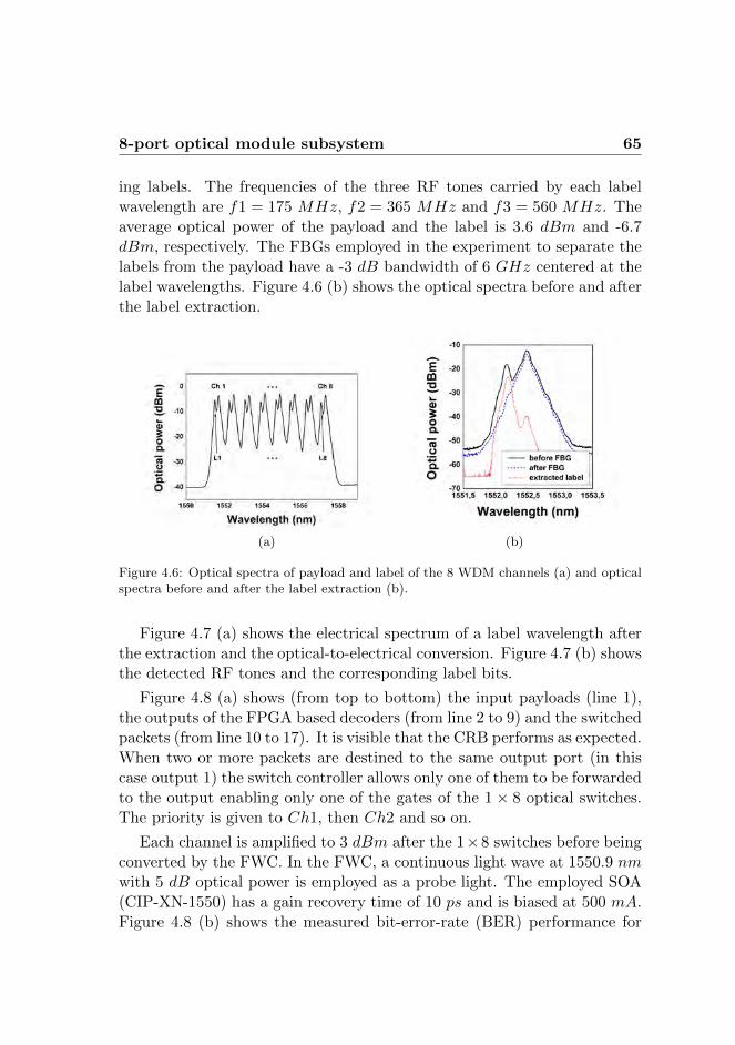
8-port optical module subsystem 65
ing labels. The frequencies of the three RF tones carried by each labelwavelength are f1 = 175 MHz, f2 = 365 MHz and f3 = 560 MHz. Theaverage optical power of the payload and the label is 3.6 dBm and -6.7dBm, respectively. The FBGs employed in the experiment to separate thelabels from the payload have a -3 dB bandwidth of 6 GHz centered at thelabel wavelengths. Figure 4.6 (b) shows the optical spectra before and afterthe label extraction.
(a) (b)
Figure 4.6: Optical spectra of payload and label of the 8 WDM channels (a) and opticalspectra before and after the label extraction (b).
Figure 4.7 (a) shows the electrical spectrum of a label wavelength afterthe extraction and the optical-to-electrical conversion. Figure 4.7 (b) showsthe detected RF tones and the corresponding label bits.
Figure 4.8 (a) shows (from top to bottom) the input payloads (line 1),the outputs of the FPGA based decoders (from line 2 to 9) and the switchedpackets (from line 10 to 17). It is visible that the CRB performs as expected.When two or more packets are destined to the same output port (in thiscase output 1) the switch controller allows only one of them to be forwardedto the output enabling only one of the gates of the 1 × 8 optical switches.The priority is given to Ch1, then Ch2 and so on.
Each channel is amplified to 3 dBm after the 1×8 switches before beingconverted by the FWC. In the FWC, a continuous light wave at 1550.9 nmwith 5 dB optical power is employed as a probe light. The employed SOA(CIP-XN-1550) has a gain recovery time of 10 ps and is biased at 500 mA.Figure 4.8 (b) shows the measured bit-error-rate (BER) performance for
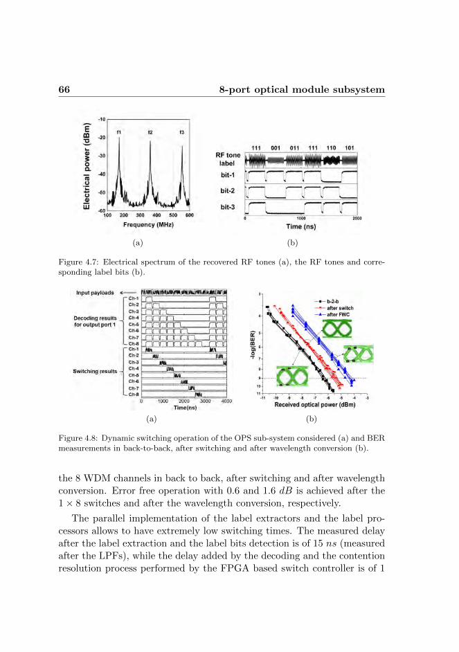
66 8-port optical module subsystem
(a) (b)
Figure 4.7: Electrical spectrum of the recovered RF tones (a), the RF tones and corre-sponding label bits (b).
(a) (b)
Figure 4.8: Dynamic switching operation of the OPS sub-system considered (a) and BERmeasurements in back-to-back, after switching and after wavelength conversion (b).
the 8 WDM channels in back to back, after switching and after wavelengthconversion. Error free operation with 0.6 and 1.6 dB is achieved after the1× 8 switches and after the wavelength conversion, respectively.
The parallel implementation of the label extractors and the label pro-cessors allows to have extremely low switching times. The measured delayafter the label extraction and the label bits detection is of 15 ns (measuredafter the LPFs), while the delay added by the decoding and the contentionresolution process performed by the FPGA based switch controller is of 1
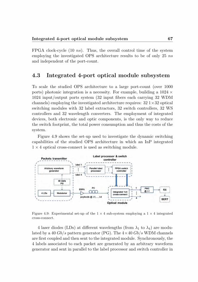
Integrated 4-port optical module subsystem 67
FPGA clock-cycle (10 ns). Thus, the overall control time of the systememploying the investigated OPS architecture results to be of only 25 nsand independent of the port-count.
4.3 Integrated 4-port optical module subsystem
To scale the studied OPS architecture to a large port-count (over 1000ports) photonic integration is a necessity. For example, building a 1024 ×1024 input/output ports system (32 input fibers each carrying 32 WDMchannels) employing the investigated architecture requires: 32 1×32 opticalswitching modules with 32 label extractors, 32 switch controllers, 32 WScontrollers and 32 wavelength converters. The employment of integrateddevices, both electronic and optic components, is the only way to reducethe switch footprint, the total power consumption and thus the costs of thesystem.
Figure 4.9 shows the set-up used to investigate the dynamic switchingcapabilities of the studied OPS architecture in which an InP integrated1× 4 optical cross-connect is used as switching module.
Figure 4.9: Experimental set-up of the 1 × 4 sub-system employing a 1 × 4 integratedcross-connect.
4 laser diodes (LDs) at different wavelengths (from λ1 to λ4) are modu-lated by a 40 Gb/s pattern generator (PG). The 4×40 Gb/s WDM channelsare first coupled and then sent to the integrated module. Synchronously, the4 labels associated to each packet are generated by an arbitrary waveformgenerator and sent in parallel to the label processor and switch controller in

68 Integrated 4-port optical module subsystem
the electrical domain. Optical labeling and optical label extraction are notstudied in this experiment. The FPGA based switch controller decodes therecovered label bits and drives the integrated device according to the pack-ets destinations. At the 4 outputs of the optical cross-connect, the trans-mitted packets (after that the contention resolution has been performed)are wavelength converted by the same FWC employed in the experiment ofthe previous section. At the output of the FWC, the packets are detectedand analyzed by a BERT.
4.3.1 Integrated optical module
The integrated device employed in the set-up as optical switching moduleis shown in Figure 4.10 (a). It is a InP monolithically integrated 4 × 4optical WDM cross-connect [86]. However, only one input of the device isused during the experiment, exploiting its 1×4 functionalities. Figure 4.10(b) shows the paths utilized during the experiment.
(a) (b)
Figure 4.10: Photograph of the 4×4 integrated optical cross-connect [86] (a) and pictureof the paths utilized during the experiment (b).
The chip has a total footprint of 4.2 mm ×3.6 mm. The cross-connectconsists of a broadcast stage (BS) and four parallel wavelength selectivestages (WSSs). The BS is realized with two cascaded 1 × 2 multi-modeinterference (MMI) splitters. At each of the four outputs of the BS a 750µm long SOA is placed to compensate the splitting losses. The BS outputsare fed into the inputs of the WSSs. Each WSS consists of a 1 × 4 cyclicAWG with a channel spacing of 3.2 nm (400 GHz) and four 140 µm long
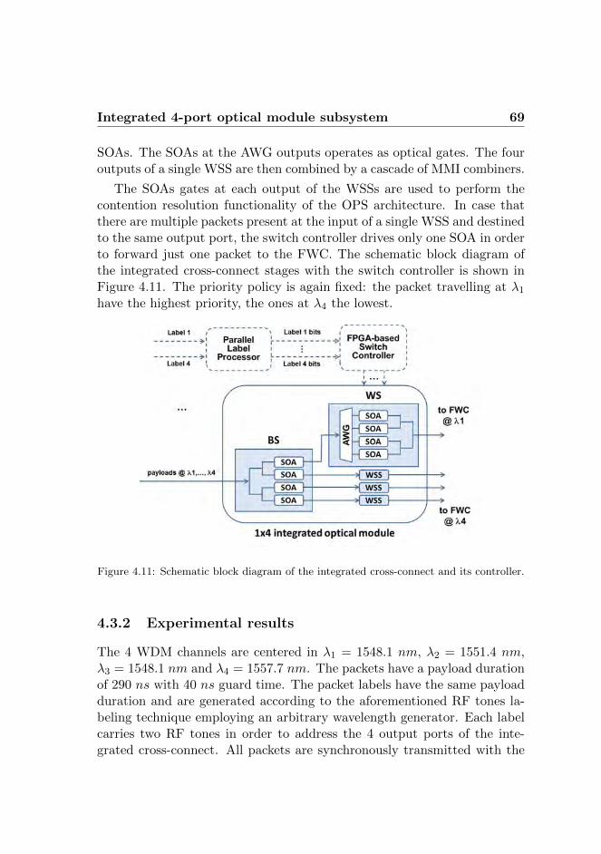
Integrated 4-port optical module subsystem 69
SOAs. The SOAs at the AWG outputs operates as optical gates. The fouroutputs of a single WSS are then combined by a cascade of MMI combiners.
The SOAs gates at each output of the WSSs are used to perform thecontention resolution functionality of the OPS architecture. In case thatthere are multiple packets present at the input of a single WSS and destinedto the same output port, the switch controller drives only one SOA in orderto forward just one packet to the FWC. The schematic block diagram ofthe integrated cross-connect stages with the switch controller is shown inFigure 4.11. The priority policy is again fixed: the packet travelling at λ1have the highest priority, the ones at λ4 the lowest.
Figure 4.11: Schematic block diagram of the integrated cross-connect and its controller.
4.3.2 Experimental results
The 4 WDM channels are centered in λ1 = 1548.1 nm, λ2 = 1551.4 nm,λ3 = 1548.1 nm and λ4 = 1557.7 nm. The packets have a payload durationof 290 ns with 40 ns guard time. The packet labels have the same payloadduration and are generated according to the aforementioned RF tones la-beling technique employing an arbitrary wavelength generator. Each labelcarries two RF tones in order to address the 4 output ports of the inte-grated cross-connect. All packets are synchronously transmitted with the
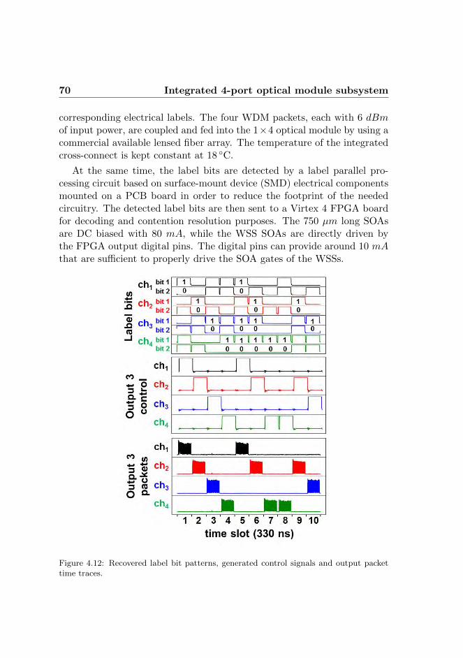
70 Integrated 4-port optical module subsystem
corresponding electrical labels. The four WDM packets, each with 6 dBmof input power, are coupled and fed into the 1×4 optical module by using acommercial available lensed fiber array. The temperature of the integratedcross-connect is kept constant at 18 ◦C.
At the same time, the label bits are detected by a label parallel pro-cessing circuit based on surface-mount device (SMD) electrical componentsmounted on a PCB board in order to reduce the footprint of the neededcircuitry. The detected label bits are then sent to a Virtex 4 FPGA boardfor decoding and contention resolution purposes. The 750 µm long SOAsare DC biased with 80 mA, while the WSS SOAs are directly driven bythe FPGA output digital pins. The digital pins can provide around 10 mAthat are sufficient to properly drive the SOA gates of the WSSs.
Figure 4.12: Recovered label bit patterns, generated control signals and output packettime traces.
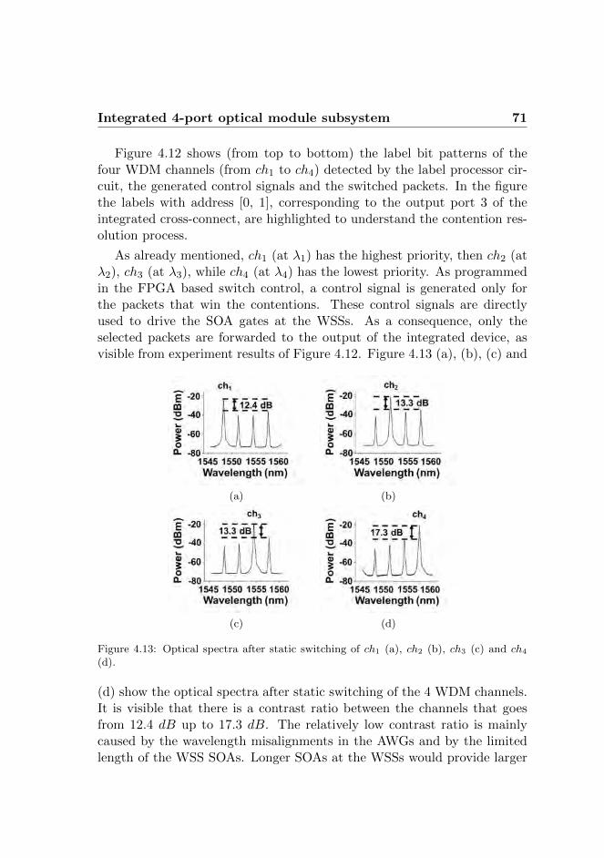
Integrated 4-port optical module subsystem 71
Figure 4.12 shows (from top to bottom) the label bit patterns of thefour WDM channels (from ch1 to ch4) detected by the label processor cir-cuit, the generated control signals and the switched packets. In the figurethe labels with address [0, 1], corresponding to the output port 3 of theintegrated cross-connect, are highlighted to understand the contention res-olution process.
As already mentioned, ch1 (at λ1) has the highest priority, then ch2 (atλ2), ch3 (at λ3), while ch4 (at λ4) has the lowest priority. As programmedin the FPGA based switch control, a control signal is generated only forthe packets that win the contentions. These control signals are directlyused to drive the SOA gates at the WSSs. As a consequence, only theselected packets are forwarded to the output of the integrated device, asvisible from experiment results of Figure 4.12. Figure 4.13 (a), (b), (c) and
(a) (b)
(c) (d)
Figure 4.13: Optical spectra after static switching of ch1 (a), ch2 (b), ch3 (c) and ch4
(d).
(d) show the optical spectra after static switching of the 4 WDM channels.It is visible that there is a contrast ratio between the channels that goesfrom 12.4 dB up to 17.3 dB. The relatively low contrast ratio is mainlycaused by the wavelength misalignments in the AWGs and by the limitedlength of the WSS SOAs. Longer SOAs at the WSSs would provide larger
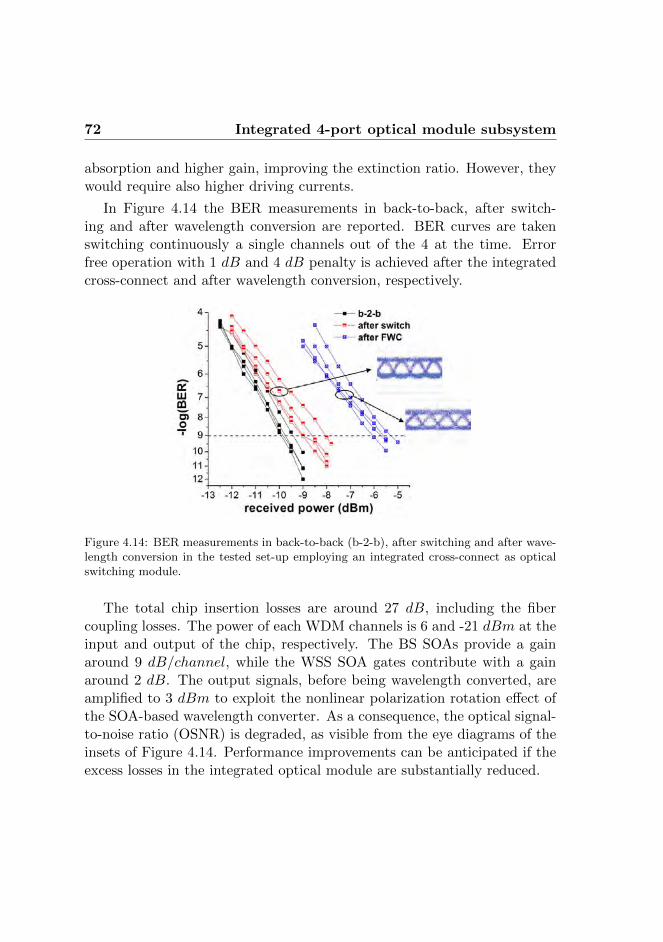
72 Integrated 4-port optical module subsystem
absorption and higher gain, improving the extinction ratio. However, theywould require also higher driving currents.
In Figure 4.14 the BER measurements in back-to-back, after switch-ing and after wavelength conversion are reported. BER curves are takenswitching continuously a single channels out of the 4 at the time. Errorfree operation with 1 dB and 4 dB penalty is achieved after the integratedcross-connect and after wavelength conversion, respectively.
Figure 4.14: BER measurements in back-to-back (b-2-b), after switching and after wave-length conversion in the tested set-up employing an integrated cross-connect as opticalswitching module.
The total chip insertion losses are around 27 dB, including the fibercoupling losses. The power of each WDM channels is 6 and -21 dBm at theinput and output of the chip, respectively. The BS SOAs provide a gainaround 9 dB/channel, while the WSS SOA gates contribute with a gainaround 2 dB. The output signals, before being wavelength converted, areamplified to 3 dBm to exploit the nonlinear polarization rotation effect ofthe SOA-based wavelength converter. As a consequence, the optical signal-to-noise ratio (OSNR) is degraded, as visible from the eye diagrams of theinsets of Figure 4.14. Performance improvements can be anticipated if theexcess losses in the integrated optical module are substantially reduced.
Discussion 73
4.4 Discussion
For the first time, a subsystem of the studied modular OPS architecture isimplemented and tested in two different experimental set-up. The subsys-tem allows to investigate the dynamic switching performances of the overallarchitecture since each module (and the corresponding controllers) operatesindependently.
Labeling technique
It is important to mention the RF tones in-band labeling technique em-ployed in this work. The technique relies on in-band (with the packet pay-load) label wavelengths each of them carrying binary-coded RF carriers.Using this method it is possible to address a large number of destinationports. Besides the spectral efficiency of the used labeling technique, the RFtones in-band labels allow for fast and parallel label detection and process-ing, performed by a label bits detection circuitry and by a FPGA basedlabel processor and switch controller in the experiments. The overall time todetect the label bits, decode the packet destinations, solve the contentionsand generate the control signals to drive the optical packet switch module isin the nanosecond scale (25 ns) and independent of the module port-count.Since all the modules can operate in parallel and autonomously, this is alsothe time to configure the overall switching matrix.
Experimental results
In the first experiment, the switching performances of a 1×8 broadcast andselect optical module subsystem build up with discrete optical componentsare investigated. Label detection, label processing, 1× 8 switch controllingand dynamic switching of 8 WDM channels at 40 Gb/s are demonstratedto operate correctly. Error free operation is achieved with 0.6 dB and 1.6dB penalty after switching and after wavelength conversion, respectively.This experiment is a proof of concept of the feasibility of the proposednovel OPS architecture and its control system. To scale the architectureto a large port-count, reducing the optical module footprint and energyconsumption, and thus to reduce the system costs, photonic integration isa crucial necessity.
74 Discussion
For this reason, the implementation of the novel OPS architecture em-ploying an integrated 1 × 4 optical cross-connect is studied in a secondexperiment. In this case, the full functional module subsystem is shown tooperate with 4 WDM channels at 40 Gb/s. Error free operation is achievedwith 1 dB and 4 dB penalty after switching (at the integrated optical cross-connect outputs) and after wavelength conversion, respectively. Comparingthese results with the ones obtained in the previous experiment, it is visiblethat around 2.5 dB of extra penalty are obtained employing the integratedcross-connect. This is due to the low power at the output of the chip andthe subsequential OSNR signal degradation due to high signal amplifica-tion. Reducing the input/output coupling losses, will reduce the perfor-mance differences between the two studied systems. SOA-based switchesare preferable over other technologies (such us Mach-Zehnder switches) dueto the high number of switching elements required by the broadcast andselect switch architecture considered. Moreover, SOA are easily integrable,can provide gain to compensate the splitting losses and can be driven innanosecond time scales between the on and off state with limited drivingcurrents. The broadcast and select architecture of the switching module isrequired to enable multicast and broadcast operations (not investigated inthis work although feasible).
Scalability
Semiconductor optical amplifiers (SOAs) are commonly employed as basicswitching elements for building larger switching matrices. They can provideoptical gain in the ON state, large absorption in the OFF state and nsswitching times [87]. Moreover, SOA based switches can be integrated.Different switch architectures have been employed to realize SOA basedswitches, like tree or Clos architectures [88, 89]. However, scaling theseswitches to large port-count is still an open challenge. Many considerationscan be made about the possibility of scaling these architectures to a highnumber of ports, like split/combine losses at the input and output, largenumber of SOA gates required or large number of cascaded SOAs in eachstage with subsequent signal distortions. The employed switch architectureplays a dominant role in this context.
The proposed OPS architecture relies on the employment of 1×F WDMoptical switching modules. Each optical switching module is based on two
Discussion 75
cascaded stages: a broadcast stage (BS) and F parallel wavelength selectivestages (WSSs). The scalability of such modules is mainly limited by thesplitting losses of the BS. These losses are proportional with the port-countof the system. Consider, for example, the integrated 1 × 4 optical cross-connect of Section 4.3.1. The BS contributes with a minimum of 6 dBon the total on-chip losses due to the two cascaded 1 × 2 MMI splitters.Increasing the number of ports would imply adding more cascaded MMIsplitters and thus more losses. The losses of the BS scale as 3 log2 (F )(dB). In the employed integrated cross-connect, SOAs are employed tocompensate the splitting losses of the BS. Longer SOAs could be employedin the design of a larger port-count switching module.
At the outputs of the employed chip, the WDM channels are combinedby means of cascaded 2× 1 MMI couplers. According to the OPS moduleoperations, the MMI couplers of the WSS outputs couple WDM channelstravelling on different wavelengths (see Figure 4.5). It is possible then toreduce the losses at this stage by replacing the couplers with an AWG. Usingan AWG, the losses at the WSSs can be reduced to 3-4 dB independently ofthe number of wavelength channels that have to be multiplexed. However,also in this case, there are technological and fabrication impairments toconsider. In fact, AWGs with high extinction ratio and low inter-channelcrosstalk are required.
However, employing WDM in the OPS module operation helps reducingthe number of ports required by each optical switching module. For ex-ample, scaling the proposed OPS architecture to 1024 input/output portsrequires the employment of 1024 optical switching modules. Considering,for example, that each input carries 32 distinct wavelength channels thenumber of output ports of each 1 × F optical switch is reduced to 32. Ingeneral, considering the number of input fibers F equal to the number ofwavelength channels M carried by each fiber (F = M = N), the opticalswitching module port-count scales as
√N . A 1×32 optical switch module
translates in 15 dB losses in the broadcast stage, and in the need of 32-channel 100 GHz spaced AWGs with flat low loss operation and over 1000SOAs integrated on the chip. Also, the SOAs employed to compensate thesplitting losses should not introduce non-linear effects. In addition, opticalsignal-to-noise ratio (OSNR) degradation and chip-coupling losses have tobe considered.
However, the implementation of the proposed architecture set a promis-
76 Summary
ing breakthrough to the realization of a large port-count integrated OPSthat could be employed in a DC environment.
4.5 Summary
The dynamic switching capabilities of the studied OPS architecture areinvestigated for the first time in two different experimental set-up. Allthe functionalities of the novel architecture, with the exception of the flowcontrol mechanism, are implemented.
The results of two experiments are presented. In the first experiment,a 1× 8 switching subsystem is investigated employing LiNbO3 switches asswitching modules. 8×40 Gb/s WDM packets with RF tones in-band opti-cal label are injected into the studied system. Labels extraction (based onFBGs and optical circulators), labels processing, switch control and con-tention resolution are shown to operate in only 25 ns. Error free operationis achieved with 0.6 and 1.6 dB penalty after switching and after wave-length conversion, respectively. The results indicates that it is feasible torealize a 64 × 64 (8 input fibers each of them carrying 8 WDM channels)OPS employing the tested 1× 8 switching sub-system.
In the second experiment, the feasibility of a 16 × 16 (4 input fiberseach of them carrying 4 WDM channels) OPS which employs integratedoptical switching modules is demonstrated. 4 × 40 Gb/s WDM packetsare injected into an 1 × 4 InP integrated optical cross-connect. Error freeoperation is shown with 1 and 4 dB penalty after the switch and after thewavelength conversion, respectively. The extra penalty obtained testingthe 1× 4 subsystem which employs the integrated cross-connect is mainlycaused by the high on-chip losses.
Chapter 5
Flow control implementation
In this chapter1, the implementation of the flow control functionality is in-vestigated. Two experiments are presented. In the first set-up, the flowcontrol functionality is implemented in the electronic domain by bufferingthe packet labels. Real-time operation of a random packet generator withvariable load, FIFO queue packet storing, buffer management for packetretransmission, contention resolution and fast switch configuration controlare implemented by using an FPGA. The optical packet payloads are im-plemented with pseudo-random bit sequences from a pulse pattern genera-tor. The flow control mechanism is successfully tested with periodic inputpacket sequences of 4 WDM channels at 40 Gb/s employing a fixed priorityalgorithm. Packet loss rate and buffer occupancy in a system with 4 and8 input channels are then investigated under random traffic conditions andemploying a round robin algorithm as priority policy. In the second set-up,an all-optical, low latency and spectral efficient flow control is implementedand tested. 2 × 40 Gb/s WDM packets with RF tones in-band optical la-bels are sent into a bidirectional system. The optical power of the extracted
1Based on the results published in: S. Di Lucente, J. Luo, A. Rohit, K.A. Williams,H.J.S. Dorren, and N. Calabretta, “Optical Packet Switch Node with Packet Flow Con-trol for Flat Inter-Cluster Data Center Network”, in Proc. of Optical Fiber Communica-tion/National Fiber Optic Engineers Conference (OFC/NFOC), Anaheim, USA., 17-21,March, 2013, Paper OW3H.4. [90], W. Miao, S. Di Lucente, J. Luo, H.J.S. Dorren, andN. Calabretta,“Low Latency and Efficient Optical Flow Control for Intra Data CenterNetworks”, European Conference and Exhibition on Optical Communication, London,UK, 2013. [91]
78 FPGA-based flow control
wavelength labels is split in two parts. The first part is sent to the labelprocessor, while the second one is re-modulated by an SOA driven by theacknowledgement message generated by the switch controller. The switchcontroller employs a fixed priority scheme in this case. The robustness ofthe flow control implementation is investigated and the packet payloads areevaluated by a BERT after the label extraction.
5.1 FPGA-based flow control
Flow controlled optical packet switch operations are investigated in theexperimental set-up shown in Figure 5.1.
A time slotted system is considered. The set-up can be split in twolayers. The upper layer, where the traffic generation, the packet buffering,the switch control, the contention resolution and the flow control mech-anism are implemented in the electronic domain by using an FPGA. Inthe bottom layer, the packet payload generation and the optical switchingmodule are fully implemented in the optical domain. At each time step,the packet payload generators create optical packets at 4 distinct WDMchannels (indicated as ch1, ch2, ch3 and ch4). Synchronously, four inde-pendent traffic generators, implemented on the FPGA, generate four labels(one for each WDM channel) with uniform distributed destinations andvariable input load. The input load represents the probability of the packettime slot occupancy. For example, an input load of 0.5 indicates that thereis a probability of 50% of having a new packet at each time slot. Eachlabel is stored in a FIFO queue. The queues have a limited capacity. As aconsequence, if the queues are full and a new label is generated, the labeland the associated packet payload are lost. The buffer managers trans-mit the stored labels and simultaneously provide gate signals to the opticalgates of the corresponding channel. At the OPS node, the electrical la-bels, which determine the packet destination, are processed by the labelprocessors in the FPGA, while the gated packet payloads are forwardedto the destination ports on the set-up optical layer. If multiple packetscontend at the same time slot the same destination port, the contentionsolver selects, using a priority policy, only one packet while the others aredropped. Dropped packets need to be retransmitted. The contention solvergenerates the control signals that configure the optical module. The mod-
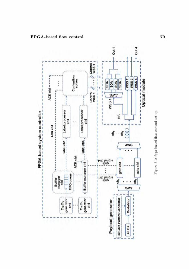
FPGA-based flow control 79
Fig
ure
5.1
:fp
ga
base
dflow
contr
ol
set-
up.
80 FPGA-based flow control
ule consists of a broadcast and select 1× 4 optical switch. The contentionsolver also generates and sends to the appropriate buffer manager a positiveacknowledgement message (ACK) for each packet that is successfully de-livered. Each buffer manager removes the label from the queue in responseto ACK. If no ACK is received the label and the payload are retransmittedafter re-signalling the input optical gates, emulating packet retransmission.
5.1.1 Experimental results
The 4×40Gb/sOOK NRZ WDM optical payloads have central wavelengthsat ch1 = 1548.1 nm, ch2 = 1551.4 nm, ch3 = 1554.5 nm and ch4 =1557.7 nm. Each payload consists of 1500 bytes (300 ns) with 30 ns ofguard band generated by modulating four LDs with a 40 Gb/s patterngenerator. The corresponding packet labels are generated in the FPGAaccording to the RF tones labeling technique described in Section 4.1. Eachlabel consists of two bits encoding the four OPS module outputs. Theemployed broadcast and select switch is the integrated 1 × 4 integratedcross-connect already described in Section 4.3.1 and operating under thesame conditions of Section 4.3.2.
To evaluate the performance of the implemented flow control mechanism,the traffic generators are programmed to create a periodic label sequenceunder specific system conditions. The traffic generator associated with ch1operates at load = 1, thus in every time slot there is a new incoming packeton this channel. The traffic generators associated with ch2, ch3 and ch4 areprogrammed to operate at load = 0.3. All traffic generators are set to in-dependently assign the labels according to a 14 time slots periodic pattern.Thus, every 14 time slots the 4 different label patterns are repeated. Thisis done to record the packet labels using an oscilloscope. The employedinput label pattern associated with ch1 and the input packet patterns of allthe channels are shown in Figure 5.2 (from top to bottom). The numbersinserted in the packet time traces indicate the packets destination ports.
The contention resolution algorithm employed in the contention solveris based on a fixed priority policy. Packets travelling on ch1 have the high-est priority, afterwards packets on ch2 and so on. The contention solvergenerates the control and the acknowledgement signals after 3 FPGA clockcycles (30 ns). Injecting the initial packet sequence in the system a periodicoutput sequence is achieved and recorded. Figure 5.3 shows, from top to
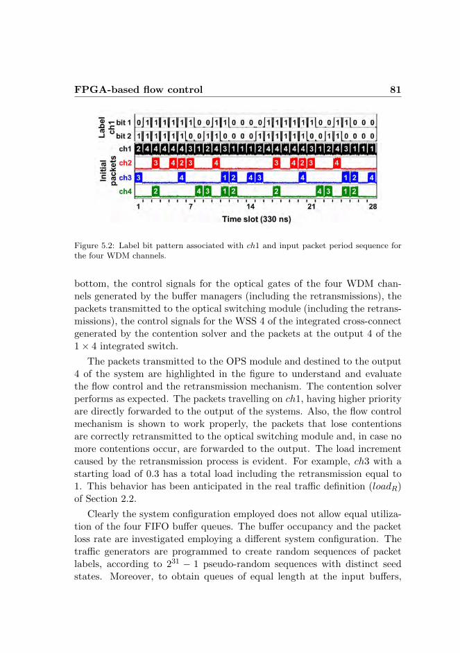
FPGA-based flow control 81
Figure 5.2: Label bit pattern associated with ch1 and input packet period sequence forthe four WDM channels.
bottom, the control signals for the optical gates of the four WDM chan-nels generated by the buffer managers (including the retransmissions), thepackets transmitted to the optical switching module (including the retrans-missions), the control signals for the WSS 4 of the integrated cross-connectgenerated by the contention solver and the packets at the output 4 of the1× 4 integrated switch.
The packets transmitted to the OPS module and destined to the output4 of the system are highlighted in the figure to understand and evaluatethe flow control and the retransmission mechanism. The contention solverperforms as expected. The packets travelling on ch1, having higher priorityare directly forwarded to the output of the systems. Also, the flow controlmechanism is shown to work properly, the packets that lose contentionsare correctly retransmitted to the optical switching module and, in case nomore contentions occur, are forwarded to the output. The load incrementcaused by the retransmission process is evident. For example, ch3 with astarting load of 0.3 has a total load including the retransmission equal to1. This behavior has been anticipated in the real traffic definition (loadR)of Section 2.2.
Clearly the system configuration employed does not allow equal utiliza-tion of the four FIFO buffer queues. The buffer occupancy and the packetloss rate are investigated employing a different system configuration. Thetraffic generators are programmed to create random sequences of packetlabels, according to 231 − 1 pseudo-random sequences with distinct seedstates. Moreover, to obtain queues of equal length at the input buffers,
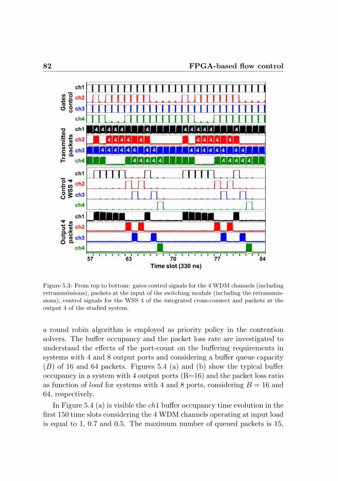
82 FPGA-based flow control
Figure 5.3: From top to bottom: gates control signals for the 4 WDM channels (includingretransmissions), packets at the input of the switching module (including the retransmis-sions), control signals for the WSS 4 of the integrated cross-connect and packets at theoutput 4 of the studied system.
a round robin algorithm is employed as priority policy in the contentionsolvers. The buffer occupancy and the packet loss rate are investigated tounderstand the effects of the port-count on the buffering requirements insystems with 4 and 8 output ports and considering a buffer queue capacity(B) of 16 and 64 packets. Figures 5.4 (a) and (b) show the typical bufferoccupancy in a system with 4 output ports (B=16) and the packet loss ratioas function of load for systems with 4 and 8 ports, considering B = 16 and64, respectively.
In Figure 5.4 (a) is visible the ch1 buffer occupancy time evolution in thefirst 150 time slots considering the 4 WDM channels operating at input loadis equal to 1, 0.7 and 0.5. The maximum number of queued packets is 15,
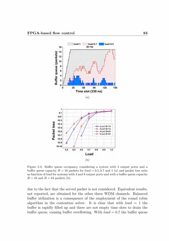
FPGA-based flow control 83
(a)
(b)
Figure 5.4: Buffer queue occupancy considering a system with 4 output ports and abuffer queue capacity B = 16 packets for load = 0.5, 0.7 and 1 (a) and packet loss ratioas function of load for systems with 4 and 8 output ports and with a buffer queue capacityB = 16 and B = 64 packets (b).
due to the fact that the served packet is not considered. Equivalent results,not reported, are obtained for the other three WDM channels. Balancedbuffer utilization is a consequence of the employment of the round robinalgorithm in the contention solver. It is clear that with load = 1 thebuffer is rapidly filled up and there are not empty time slots to drain thebuffer queue, causing buffer overflowing. With load = 0.7 the buffer queue
84 All-optical flow control
increases as function of the contentions. The buffer queue decreases whenthere are empty time slots that can be used to successfully retransmit thedropped packets. With load = 0.5, the buffer is never full during thestudied time slots, suggesting that a buffer queue capacity of 16 packets isenough to avoid packet losses in the system under this traffic load.
Figure 5.4 (b) shows the packet loss performance of the system consider-ing 1012 time slots. Once again, the Figure refers to ch1 and the equivalentresults for the other channels are omitted. The curves are obtained consid-ering an OPS switching module with 4 and 8 output ports and considering abuffer capacity of 16 and 64 packets. The results reveal that, for load ≥ 0.8,the packet loss is port-count and buffer capacity independent. Consideringlower load, the packet loss performance of the system improves increasingthe buffer capacity and degrades increasing the number of ports. For ex-ample, with laod ' 0.6 a buffer capacity of 16 packets allows a packet lossaround 10−2 for both the 4-port and the 8-port cases. At the same loadvalue a buffer capacity of 64 packets ensures a packet loss around 10−7
for a 4-port system and a packet loss around 10−5 for a 64-port system.This behavior is in agreement with the results of the simulated systems ofChapter 3.
5.2 All-optical flow control
Although having separated electrical paths that enable the flow controlfunctionality of the studied OPS architecture is a valid solution, an efficientall-optical flow control implementation is preferable to reduce the numberof wired interconnections in a large scale system.
The idea is to use the same wavelength utilized to transmit the packetlabel to send back to the transmitting node the optical acknowledgementmessage in order to limit the number of required interconnections. Thisis investigated employing the bidirectional system depicted in Figure 5.5.2×40 Gb/s WDM channels, indicated with ch1 (at λ1) and ch2 (at λ2) withRF tones in-band optical labels are sent into the OPS packet switch sys-tem under investigation after being multiplexed by an AWG. At the OPSinput the WDM channels are demultiplexed. The label of each channel isextracted from the payload by employing an optical circulator and a FBGwith central wavelength at the label wavelength. The packet payloads re-
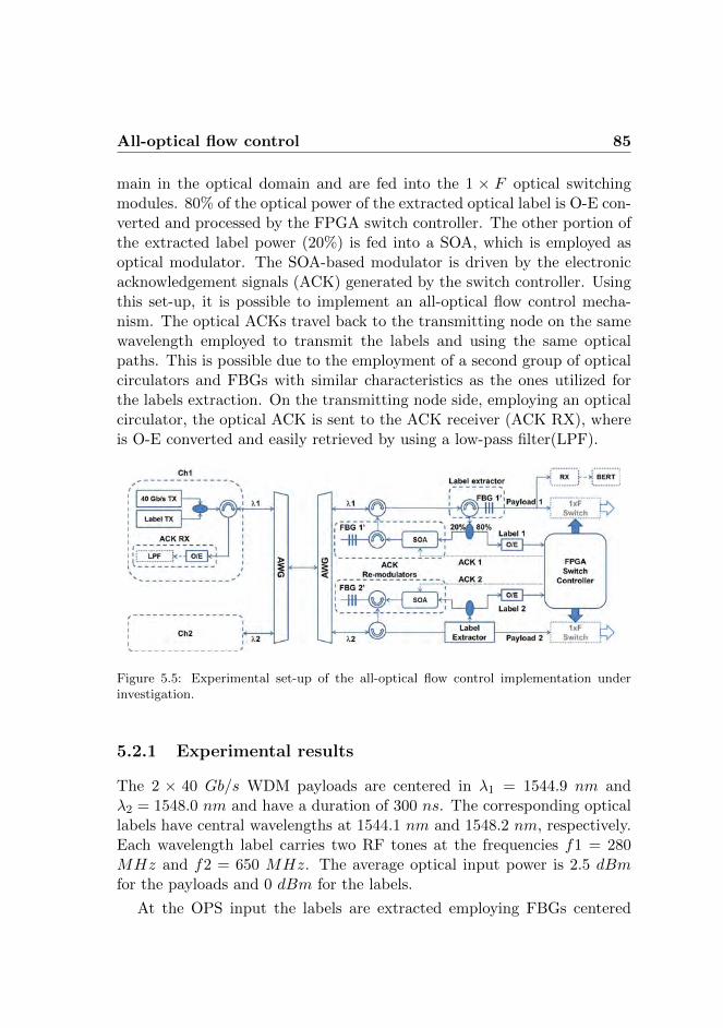
All-optical flow control 85
main in the optical domain and are fed into the 1 × F optical switchingmodules. 80% of the optical power of the extracted optical label is O-E con-verted and processed by the FPGA switch controller. The other portion ofthe extracted label power (20%) is fed into a SOA, which is employed asoptical modulator. The SOA-based modulator is driven by the electronicacknowledgement signals (ACK) generated by the switch controller. Usingthis set-up, it is possible to implement an all-optical flow control mecha-nism. The optical ACKs travel back to the transmitting node on the samewavelength employed to transmit the labels and using the same opticalpaths. This is possible due to the employment of a second group of opticalcirculators and FBGs with similar characteristics as the ones utilized forthe labels extraction. On the transmitting node side, employing an opticalcirculator, the optical ACK is sent to the ACK receiver (ACK RX), whereis O-E converted and easily retrieved by using a low-pass filter(LPF).
Figure 5.5: Experimental set-up of the all-optical flow control implementation underinvestigation.
5.2.1 Experimental results
The 2 × 40 Gb/s WDM payloads are centered in λ1 = 1544.9 nm andλ2 = 1548.0 nm and have a duration of 300 ns. The corresponding opticallabels have central wavelengths at 1544.1 nm and 1548.2 nm, respectively.Each wavelength label carries two RF tones at the frequencies f1 = 280MHz and f2 = 650 MHz. The average optical input power is 2.5 dBmfor the payloads and 0 dBm for the labels.
At the OPS input the labels are extracted employing FBGs centered
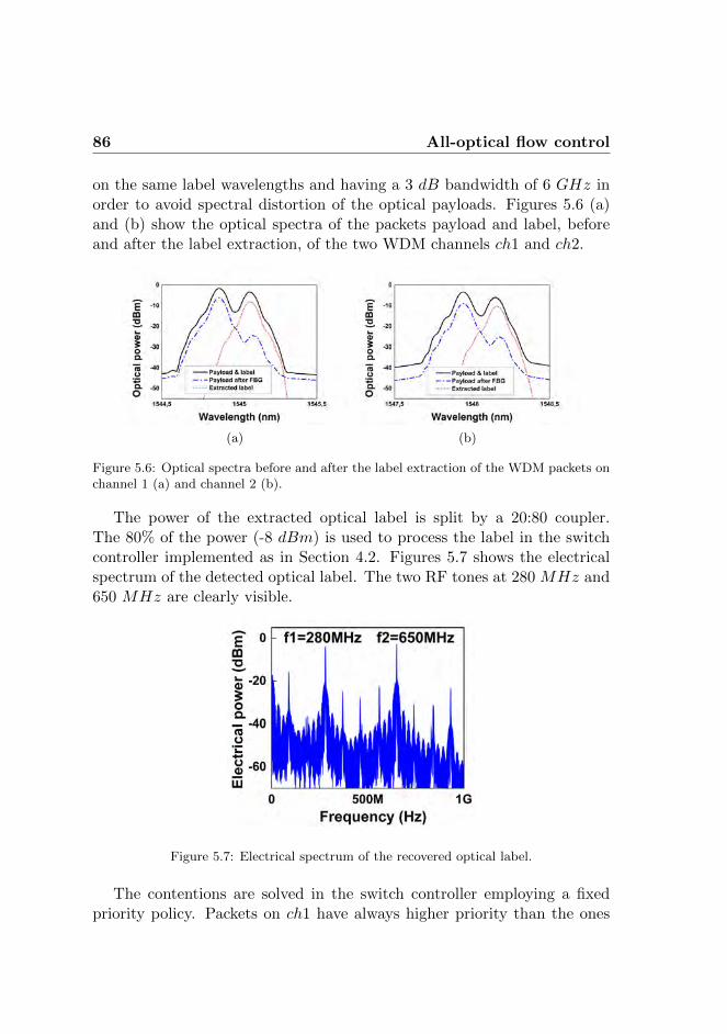
86 All-optical flow control
on the same label wavelengths and having a 3 dB bandwidth of 6 GHz inorder to avoid spectral distortion of the optical payloads. Figures 5.6 (a)and (b) show the optical spectra of the packets payload and label, beforeand after the label extraction, of the two WDM channels ch1 and ch2.
(a) (b)
Figure 5.6: Optical spectra before and after the label extraction of the WDM packets onchannel 1 (a) and channel 2 (b).
The power of the extracted optical label is split by a 20:80 coupler.The 80% of the power (-8 dBm) is used to process the label in the switchcontroller implemented as in Section 4.2. Figures 5.7 shows the electricalspectrum of the detected optical label. The two RF tones at 280 MHz and650 MHz are clearly visible.
Figure 5.7: Electrical spectrum of the recovered optical label.
The contentions are solved in the switch controller employing a fixedpriority policy. Packets on ch1 have always higher priority than the ones
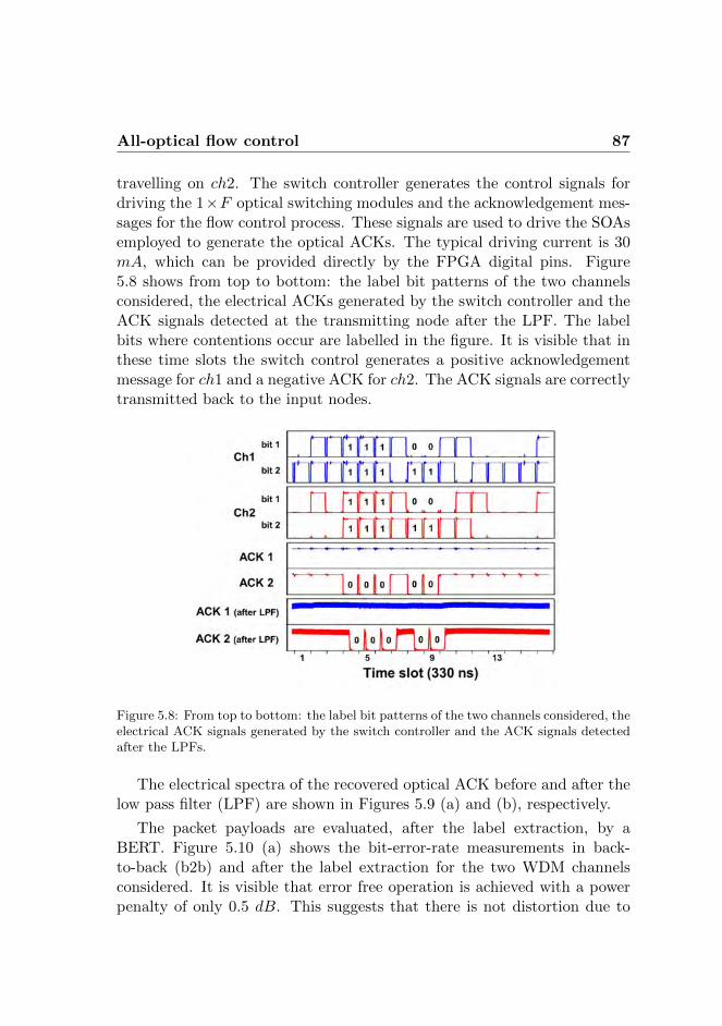
All-optical flow control 87
travelling on ch2. The switch controller generates the control signals fordriving the 1×F optical switching modules and the acknowledgement mes-sages for the flow control process. These signals are used to drive the SOAsemployed to generate the optical ACKs. The typical driving current is 30mA, which can be provided directly by the FPGA digital pins. Figure5.8 shows from top to bottom: the label bit patterns of the two channelsconsidered, the electrical ACKs generated by the switch controller and theACK signals detected at the transmitting node after the LPF. The labelbits where contentions occur are labelled in the figure. It is visible that inthese time slots the switch control generates a positive acknowledgementmessage for ch1 and a negative ACK for ch2. The ACK signals are correctlytransmitted back to the input nodes.
Figure 5.8: From top to bottom: the label bit patterns of the two channels considered, theelectrical ACK signals generated by the switch controller and the ACK signals detectedafter the LPFs.
The electrical spectra of the recovered optical ACK before and after thelow pass filter (LPF) are shown in Figures 5.9 (a) and (b), respectively.
The packet payloads are evaluated, after the label extraction, by aBERT. Figure 5.10 (a) shows the bit-error-rate measurements in back-to-back (b2b) and after the label extraction for the two WDM channelsconsidered. It is visible that error free operation is achieved with a powerpenalty of only 0.5 dB. This suggests that there is not distortion due to
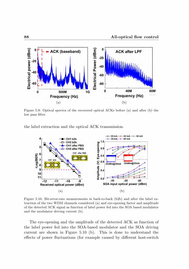
88 All-optical flow control
(a) (b)
Figure 5.9: Optical spectra of the recovered optical ACKs before (a) and after (b) thelow pass filter.
the label extraction and the optical ACK transmission.
(a) (b)
Figure 5.10: Bit-error-rate measurements in back-to-back (b2b) and after the label ex-traction of the two WDM channels considered (a) and eye-opening factor and amplitudeof the detected ACK signal as function of label power fed into the SOA based modulatorand the modulator driving current (b).
The eye-opening and the amplitude of the detected ACK as function ofthe label power fed into the SOA-based modulator and the SOA drivingcurrent are shown in Figure 5.10 (b). This is done to understand theeffects of power fluctuations (for example caused by different host-switch
Discussion 89
distances) on the implemented flow control mechanism. Figure 5.10 (b)shows that driving the SOA-based modulator with a current of 30 mAensures an eye-opening factor higher than 0.8 with input power rangingfrom -30 dBm to 18 dBm. Even larger dynamic range is achievable withhigher driving currents. As a conclusion, the system is robust to powerfluctuations and thus to distance variations within a DC network.
5.3 Discussion
Two distinct methods to implement the flow control functionality requiredto enable packet retransmission are presented in this chapter.
An FPGA-based flow control implementation is tested successfully un-der dynamic switching operation. The effects of packet retransmission onthe system load is clearly visible adopting a fixed priority policy in thecontention resolution process. A channel with low priority with a startingload of 0.3 is rapidly full loaded due to the multiple packet contentions.This phenomenon highlights the need of a more complex priority algorithmor the need of a balanced traffic pattern within the investigated system. Around robin algorithm is then used to investigate the performance in termsof packet loss of the implemented system under variable system load. Theround robin algorithm allows balanced buffer occupancy and reduces themaximum latency that a packet can experience in the system. In fact, itguarantees that each packet (except the ones lost due to buffer overflowing)is delivered to the appropriate output port after a maximum of three lostcontentions, since within the fourth attempt it will be travelling on thechannel with highest priority.
The system studied shows no losses for input load up to 0.4, this valueis higher than the typical DC traffic load. Increasing the system port-count (from 4 to 8), the packet loss performance degrades. However, thisdegradation becomes negligible under heavy traffic load (≥ 0.6). On thecontrary, better packet loss results are achieved considering a larger buffercapacity. Increasing the buffer capacity from 16 to 64 packets lead to losslesssystems for load up to 0.5 and 0.6 for the 8-port case and the 4-port case,respectively.
However, an all-optical solution is preferable since it does not require adedicated interconnections network to be implemented. A large-scale sys-
90 Summary
tem such as a data center requires a large number of wired interconnections.Exploiting added functionalities on the already deployed optical cables is avalid solution.
The proposed all-optical implementation of the flow control functionalityis based on the reutilization of part of the optical power of the optical packetlabel. Few extra components are required for its implementation and thesame optical path used for the packet transmission is employed also for thetransmission of an optical acknowledgement back to the transmitting node.This solution is resource and spectral efficient.
This implementation is experimentally tested and the results show thatit does not degrade the packet payload quality as confirmed by the bit-error-rate curves. Also, the limited portion of optical label power (20%),employed to generate the optical acknowledgement, does not affect the labeldetection.
A limited number of extra components are required for this implemen-tation: a semiconductor optical amplifier (per channel) is required to mod-ulate the optical label wavelength and a fiber Bragg grating in combinationwith an optical circulator is needed to couple the generated signals back inthe packet transmission path. This implementation requires also an addi-tional receiver (in combination with a low-pass filter) at the transmittingnode to detect the optical acknowledge message. The all-optical flow controlimplementation is also shown to be robust to power fluctuations.
The functionalities implemented by using fiber Bragg gratings and opti-cal circulators (label extraction and optical acknowledgement generation)can be implemented using integrated microring resonators (MRRs). Theimplementation of an integrated label extractor based on MMRs is dis-cussed in the next chapter of this thesis.
5.4 Summary
Two different implementations of the flow control mechanism that allowspacket retransmission in a DC inter-cluster network which employs the OPSarchitecture under investigation are presented. In the first one, a dedica-ted electronic network is employed for the acknowledgement signals gen-eration and transmission. Traffic generation, packet label buffering, labelprocessors, switch control, contention resolution functionality and acknowl-
Summary 91
edgement signals generation and transmission are implemented by using anFPGA. Optical packet payload generation and switching process are per-formed in the optical domain. 4 × 40 Gb/s WDM packets are sent intoan integrated optical cross-connect. The flow control functionality is suc-cessfully implemented and demonstrated. The system is tested injectingperiodic packet patterns under constrained system configurations to obtaina periodic response, needed to record the signals. Buffer requirements andpacket loss performance are investigated considering a random input trafficand different buffer capacities. The results reveal that the performancesof the system are port-count and buffer-size independent for load ≥ 0.8.For lower load the performance degrades increasing the port-count and de-creasing the buffer capacity.
Having a dedicated electrical network for the flow control functionalitymay be cumbersome considering the number of wired interconnections re-quired in a large scale data center. For this reason, the second experimentalset-up is used to investigate an all-optical solution. The employed bidirec-tional system utilizes part of the power of the extracted optical packetlabel to generate the optical ACK. A SOA-based modulator driven by theFPGA controller and optical circulators in combination with FBGs areused to generate and transmit the optical acknowledge signals employingthe same wavelength and the same optical path of the optical packet la-bel. At the receiver side (the packet transmitting node) the optical ACKis O-E converted and retrieved by employing a LPF. The all-optical im-plementation is shown to operate correctly injecting 2 × 40 Gb/s WDMpackets with in-band labels in the system. The packet payloads are eval-uated, after the label extraction, by means of BER measurements. Errorfree operation is achieved with a penalty of only 0.5 dB. The robustness ofthe optical ACK, in terms of amplitude and eye-opening, as function of thepower of the extracted label used for the ACK generation and as functionon the SOA-based modulator driving current is investigated. The resultsreveal that, considering a driving current of 30 mA, the eye-opening factoris larger than 0.8 with an input power range between −30 dBm and −18dBm. Even larger power ranges can be achieved driving the SOA basedmodulator with higher currents. Thus, this flow control implementationresults to be robust to possible power fluctuations in a DC environment.

Chapter 6
Towards the total OPSintegration
In this chapter1, the photonic integration of the novel OPS architecture isinvestigated. Toward this goal, the performances of a SOI integrated labelextractor are investigated in an experimental set-up. The studied deviceconsists of four cascaded microring resonators. Three in-band RF tones la-bel wavelengths are coupled with a 160 Gb/s packet payload and sent intothe chip for the label extraction process. Extracted labels are processedby a FPGA-based switch controller, while packet payload is evaluated bya BERT after the filtering process. In a second experimental set-up, a SOIintegrated device which includes an AWG for WDM channel demultiplex-ing and microring resonators for label extraction is tested. 3 × 40 Gb/sWDM payloads are coupled with an optical label at 1.3 Gb/s and fed intothe chip. The performances of the integrated device in terms of channeldemultiplexing and label extraction are investigated and reported.
1Based on the results published in: S. Di Lucente, P. De Heyn, D. Van Thourhout,H.J.S. Dorren, and N. Calabretta, “160 Gb/s Optical Packet Switch Module EmployingSOI Integrated Label Extractor”, Photonics in Switching (PS), Kyoto, Japan, 30 June-4July, 2013. [92], P. De Heyn, J. Luo, A. Trita, S. Pathak, S. Di Lucente, H.J.S. Dorren, N.Calabretta, and D. Van Thourhout.“A Compact Integrated 40Gb/s Packet Demultiplexerand Label Extractor on Silicon-on-Insulator for an Optical Packet Switch”, EuropeanConference and Exhibition on Optical Communication, London, UK, 2013. [93]
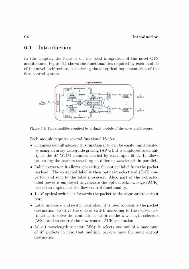
94 Introduction
6.1 Introduction
In this chapter, the focus is on the total integration of the novel OPSarchitecture. Figure 6.1 shows the functionalities required by each moduleof the novel architecture, considering the all-optical implementation of theflow control system.
Figure 6.1: Functionalities required by a single module of the novel architecture.
Each module requires several functional blocks:
• Channels demultiplexer: this functionality can be easily implementedby using an array waveguide grating (AWG). It is employed to demul-tiplex the M WDM channels carried by each input fiber. It allowsprocessing the packets travelling on different wavelength in parallel.
• Label extractor: it allows separating the optical label from the packetpayload. The extracted label is then optical-to-electrical (O-E) con-verted and sent to the label processor. Also, part of the extractedlabel power is employed to generate the optical acknowledge (ACK)needed to implement the flow control functionality.
• 1×F optical switch: it forwards the packet to the appropriate outputport.
• Label processor and switch controller: it is used to identify the packetdestination, to drive the optical switch according to the packet des-tination, to solve the contentions, to drive the wavelength selectors(WSs) and to control the flow control ACK generation.
• M × 1 wavelength selector (WS): it selects one out of a maximumof M packets in case that multiple packets have the same outputdestination.
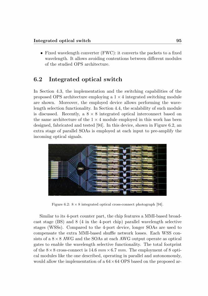
Integrated optical switch 95
• Fixed wavelength converter (FWC): it converts the packets to a fixedwavelength. It allows avoiding contentions between different modulesof the studied OPS architecture.
6.2 Integrated optical switch
In Section 4.3, the implementation and the switching capabilities of theproposed OPS architecture employing a 1× 4 integrated switching moduleare shown. Moreover, the employed device allows performing the wave-length selection functionality. In Section 4.4, the scalability of such moduleis discussed. Recently, a 8 × 8 integrated optical interconnect based onthe same architecture of the 1× 4 module employed in this work has beendesigned, fabricated and tested [94]. In this device, shown in Figure 6.2, anextra stage of parallel SOAs is employed at each input to pre-amplify theincoming optical signals.
Figure 6.2: 8 × 8 integrated optical cross-connect photograph [94].
Similar to its 4-port counter part, the chip features a MMI-based broad-cast stage (BS) and 8 (4 in the 4-port chip) parallel wavelength selectivestages (WSSs). Compared to the 4-port device, longer SOAs are used tocompensate the extra MMI-based shuffle network losses. Each WSS con-sists of a 8×8 AWG and the SOAs at each AWG output operate as opticalgates to enable the wavelength selective functionality. The total footprintof the 8×8 cross-connect is 14.6 mm×6.7 mm. The employment of 8 opti-cal modules like the one described, operating in parallel and autonomously,would allow the implementation of a 64×64 OPS based on the proposed ar-
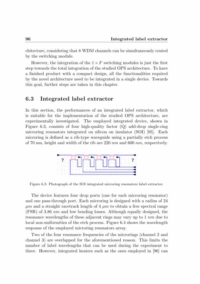
96 Integrated label extractor
chitecture, considering that 8 WDM channels can be simultaneously routedby the switching module.
However, the integration of the 1×F switching modules is just the firststep towards the total integration of the studied OPS architecture. To havea finished product with a compact design, all the functionalities requiredby the novel architecture need to be integrated in a single device. Towardsthis goal, further steps are taken in this chapter.
6.3 Integrated label extractor
In this section, the performances of an integrated label extractor, whichis suitable for the implementation of the studied OPS architecture, areexperimentally investigated. The employed integrated device, shown inFigure 6.3, consists of four high-quality factor (Q) add-drop single-ringmicroring resonators integrated on silicon on insulator (SOI) [95]. Eachmicroring is defined as a rib-type waveguide using a partially etch processof 70 nm, height and width of the rib are 220 nm and 600 nm, respectively.
Figure 6.3: Photograph of the SOI integrated microring resonators label extractor.
The device features four drop ports (one for each microring resonator)and one pass-through port. Each microring is designed with a radius of 24µm and a straight racetrack length of 4 µm to obtain a free spectral range(FSR) of 3.86 nm and low bending losses. Although equally designed, theresonance wavelengths of these adjacent rings may vary up to 1 nm due tolocal non-uniformities of the etch process. Figure 6.4 shows the wavelengthresponse of the employed microring resonators array.
Two of the four resonance frequencies of the microrings (channel 2 andchannel 3) are overlapped for the aforementioned reason. This limits thenumber of label wavelengths that can be used during the experiment tothree. However, integrated heaters such as the ones employed in [96] can
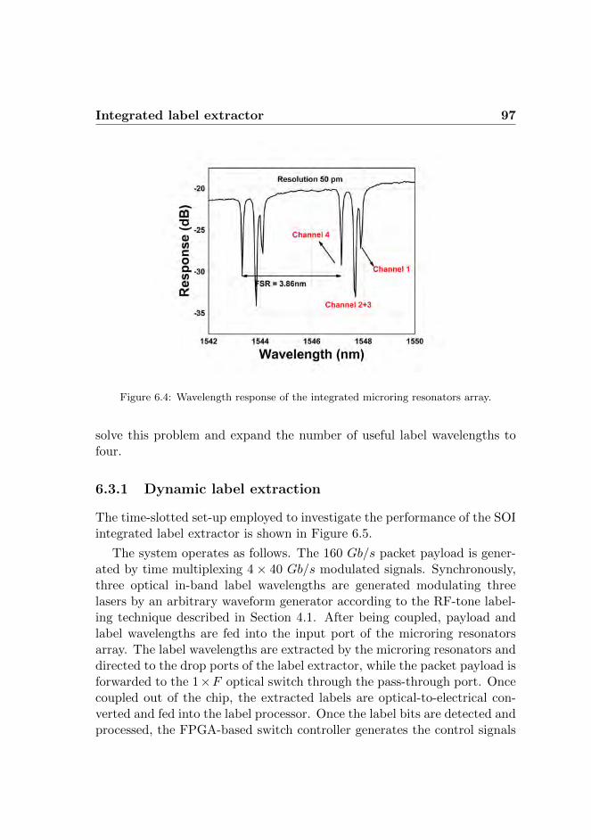
Integrated label extractor 97
Figure 6.4: Wavelength response of the integrated microring resonators array.
solve this problem and expand the number of useful label wavelengths tofour.
6.3.1 Dynamic label extraction
The time-slotted set-up employed to investigate the performance of the SOIintegrated label extractor is shown in Figure 6.5.
The system operates as follows. The 160 Gb/s packet payload is gener-ated by time multiplexing 4× 40 Gb/s modulated signals. Synchronously,three optical in-band label wavelengths are generated modulating threelasers by an arbitrary waveform generator according to the RF-tone label-ing technique described in Section 4.1. After being coupled, payload andlabel wavelengths are fed into the input port of the microring resonatorsarray. The label wavelengths are extracted by the microring resonators anddirected to the drop ports of the label extractor, while the packet payload isforwarded to the 1×F optical switch through the pass-through port. Oncecoupled out of the chip, the extracted labels are optical-to-electrical con-verted and fed into the label processor. Once the label bits are detected andprocessed, the FPGA-based switch controller generates the control signals
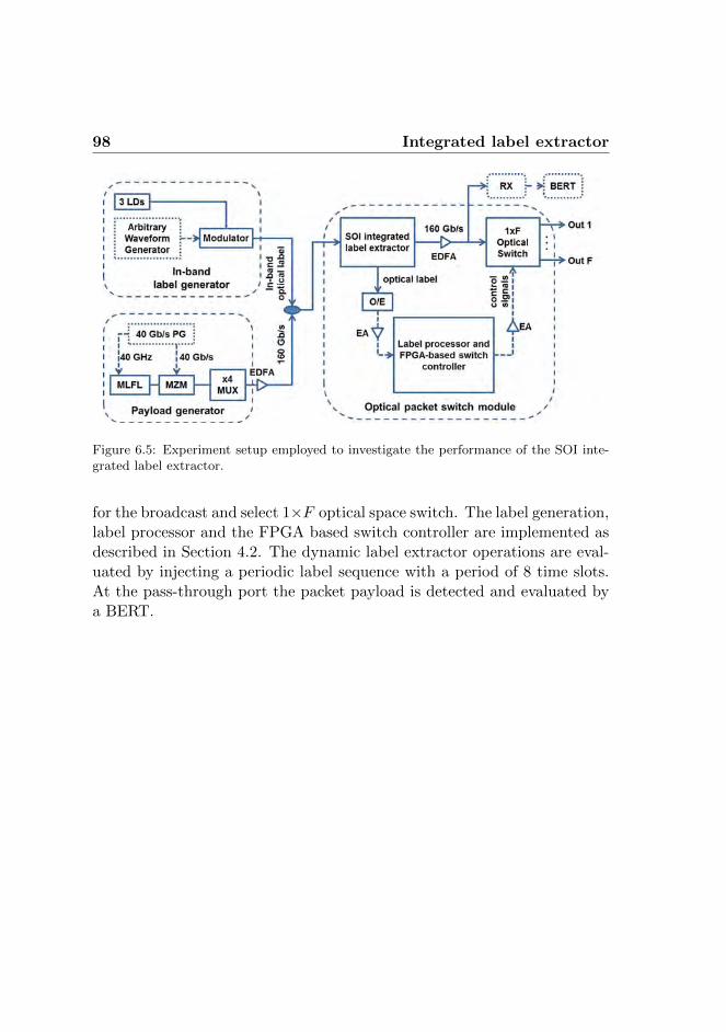
98 Integrated label extractor
Figure 6.5: Experiment setup employed to investigate the performance of the SOI inte-grated label extractor.
for the broadcast and select 1×F optical space switch. The label generation,label processor and the FPGA based switch controller are implemented asdescribed in Section 4.2. The dynamic label extractor operations are eval-uated by injecting a periodic label sequence with a period of 8 time slots.At the pass-through port the packet payload is detected and evaluated bya BERT.
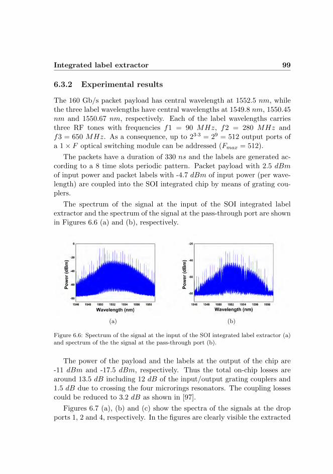
Integrated label extractor 99
6.3.2 Experimental results
The 160 Gb/s packet payload has central wavelength at 1552.5 nm, whilethe three label wavelengths have central wavelengths at 1549.8 nm, 1550.45nm and 1550.67 nm, respectively. Each of the label wavelengths carriesthree RF tones with frequencies f1 = 90 MHz, f2 = 280 MHz andf3 = 650 MHz. As a consequence, up to 23·3 = 29 = 512 output ports ofa 1× F optical switching module can be addressed (Fmax = 512).
The packets have a duration of 330 ns and the labels are generated ac-cording to a 8 time slots periodic pattern. Packet payload with 2.5 dBmof input power and packet labels with -4.7 dBm of input power (per wave-length) are coupled into the SOI integrated chip by means of grating cou-plers.
The spectrum of the signal at the input of the SOI integrated labelextractor and the spectrum of the signal at the pass-through port are shownin Figures 6.6 (a) and (b), respectively.
(a) (b)
Figure 6.6: Spectrum of the signal at the input of the SOI integrated label extractor (a)and spectrum of the the signal at the pass-through port (b).
The power of the payload and the labels at the output of the chip are-11 dBm and -17.5 dBm, respectively. Thus the total on-chip losses arearound 13.5 dB including 12 dB of the input/output grating couplers and1.5 dB due to crossing the four microrings resonators. The coupling lossescould be reduced to 3.2 dB as shown in [97].
Figures 6.7 (a), (b) and (c) show the spectra of the signals at the dropports 1, 2 and 4, respectively. In the figures are clearly visible the extracted
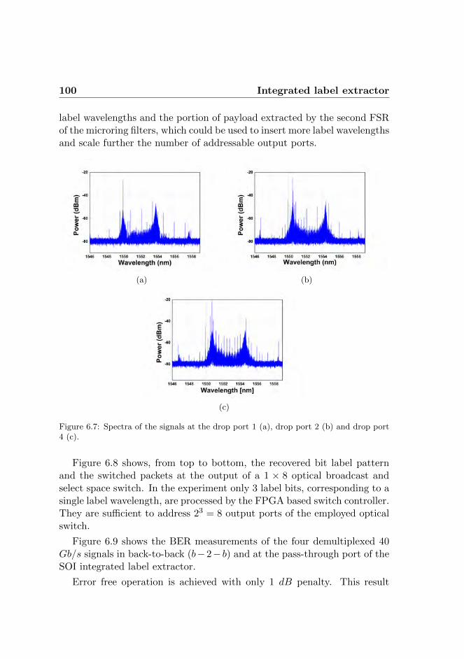
100 Integrated label extractor
label wavelengths and the portion of payload extracted by the second FSRof the microring filters, which could be used to insert more label wavelengthsand scale further the number of addressable output ports.
(a) (b)
(c)
Figure 6.7: Spectra of the signals at the drop port 1 (a), drop port 2 (b) and drop port4 (c).
Figure 6.8 shows, from top to bottom, the recovered bit label patternand the switched packets at the output of a 1 × 8 optical broadcast andselect space switch. In the experiment only 3 label bits, corresponding to asingle label wavelength, are processed by the FPGA based switch controller.They are sufficient to address 23 = 8 output ports of the employed opticalswitch.
Figure 6.9 shows the BER measurements of the four demultiplexed 40Gb/s signals in back-to-back (b−2− b) and at the pass-through port of theSOI integrated label extractor.
Error free operation is achieved with only 1 dB penalty. This result
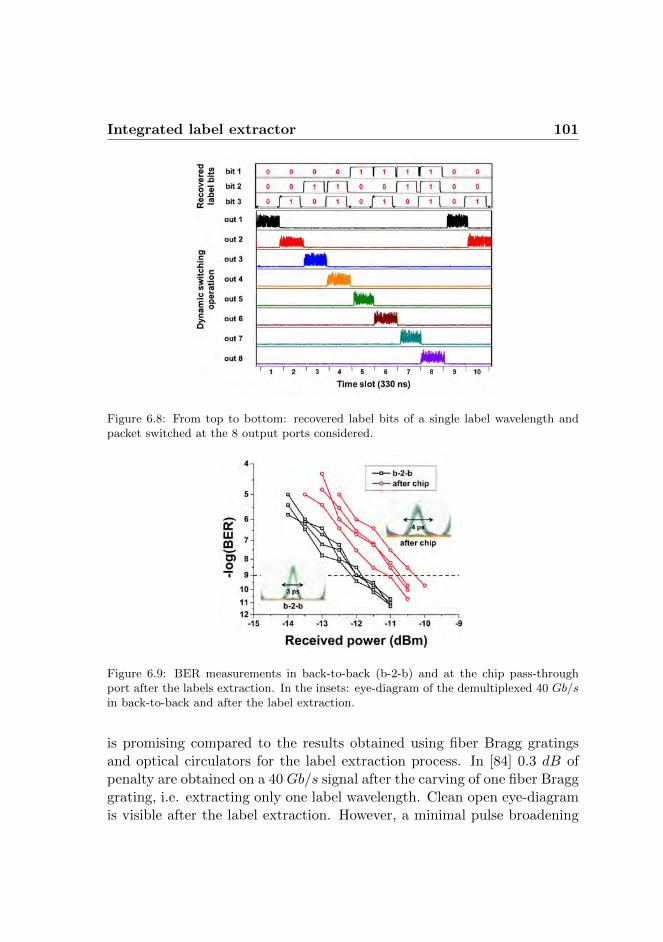
Integrated label extractor 101
Figure 6.8: From top to bottom: recovered label bits of a single label wavelength andpacket switched at the 8 output ports considered.
Figure 6.9: BER measurements in back-to-back (b-2-b) and at the chip pass-throughport after the labels extraction. In the insets: eye-diagram of the demultiplexed 40 Gb/sin back-to-back and after the label extraction.
is promising compared to the results obtained using fiber Bragg gratingsand optical circulators for the label extraction process. In [84] 0.3 dB ofpenalty are obtained on a 40 Gb/s signal after the carving of one fiber Bragggrating, i.e. extracting only one label wavelength. Clean open eye-diagramis visible after the label extraction. However, a minimal pulse broadening
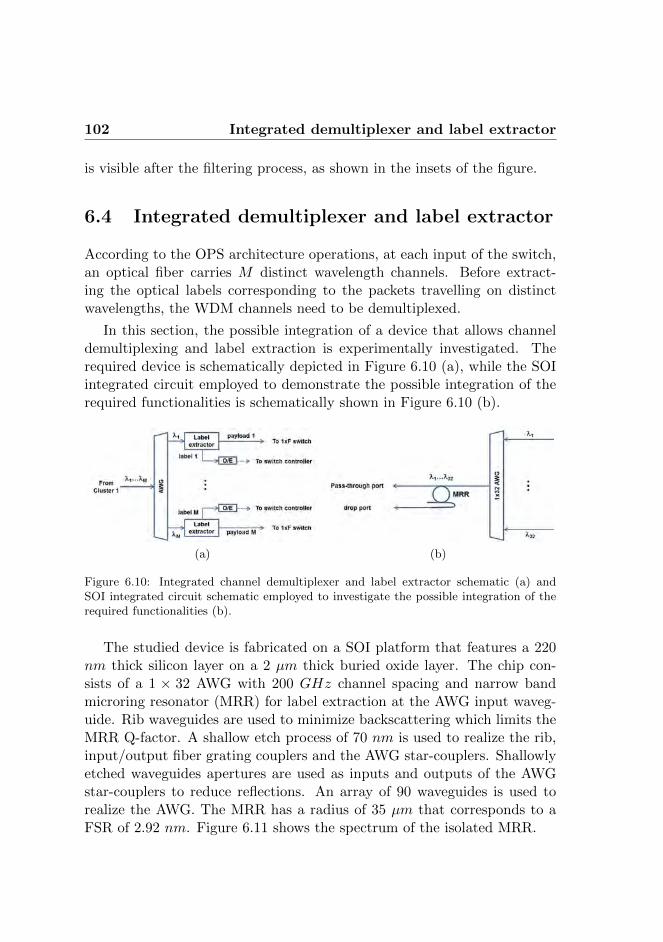
102 Integrated demultiplexer and label extractor
is visible after the filtering process, as shown in the insets of the figure.
6.4 Integrated demultiplexer and label extractor
According to the OPS architecture operations, at each input of the switch,an optical fiber carries M distinct wavelength channels. Before extract-ing the optical labels corresponding to the packets travelling on distinctwavelengths, the WDM channels need to be demultiplexed.
In this section, the possible integration of a device that allows channeldemultiplexing and label extraction is experimentally investigated. Therequired device is schematically depicted in Figure 6.10 (a), while the SOIintegrated circuit employed to demonstrate the possible integration of therequired functionalities is schematically shown in Figure 6.10 (b).
(a) (b)
Figure 6.10: Integrated channel demultiplexer and label extractor schematic (a) andSOI integrated circuit schematic employed to investigate the possible integration of therequired functionalities (b).
The studied device is fabricated on a SOI platform that features a 220nm thick silicon layer on a 2 µm thick buried oxide layer. The chip con-sists of a 1 × 32 AWG with 200 GHz channel spacing and narrow bandmicroring resonator (MRR) for label extraction at the AWG input waveg-uide. Rib waveguides are used to minimize backscattering which limits theMRR Q-factor. A shallow etch process of 70 nm is used to realize the rib,input/output fiber grating couplers and the AWG star-couplers. Shallowlyetched waveguides apertures are used as inputs and outputs of the AWGstar-couplers to reduce reflections. An array of 90 waveguides is used torealize the AWG. The MRR has a radius of 35 µm that corresponds to aFSR of 2.92 nm. Figure 6.11 shows the spectrum of the isolated MRR.
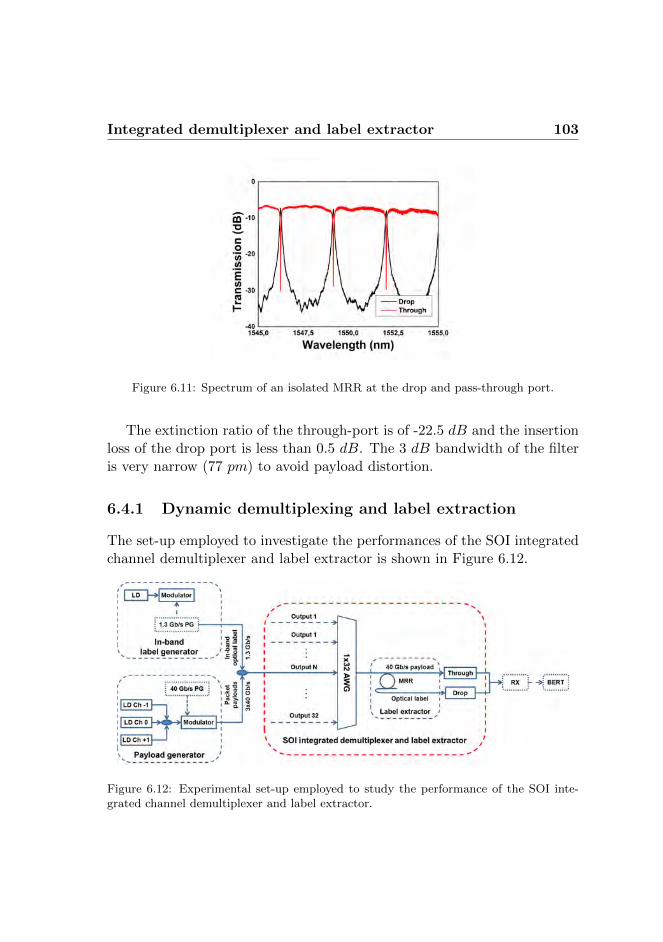
Integrated demultiplexer and label extractor 103
Figure 6.11: Spectrum of an isolated MRR at the drop and pass-through port.
The extinction ratio of the through-port is of -22.5 dB and the insertionloss of the drop port is less than 0.5 dB. The 3 dB bandwidth of the filteris very narrow (77 pm) to avoid payload distortion.
6.4.1 Dynamic demultiplexing and label extraction
The set-up employed to investigate the performances of the SOI integratedchannel demultiplexer and label extractor is shown in Figure 6.12.
Figure 6.12: Experimental set-up employed to study the performance of the SOI inte-grated channel demultiplexer and label extractor.
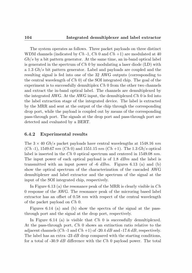
104 Integrated demultiplexer and label extractor
The system operates as follows. Three packet payloads on three distinctWDM channels (indicated by Ch -1, Ch 0 and Ch +1) are modulated at 40Gb/s by a bit pattern generator. At the same time, an in-band optical labelis generated in the spectrum of Ch 0 by modulating a laser diode (LD) witha 1.3 Gb/s bit pattern generator. Label and payloads are coupled and theresulting signal is fed into one of the 32 AWG outputs (corresponding tothe central wavelength of Ch 0) of the SOI integrated chip. The goal of theexperiment is to successfully demultiplex Ch 0 from the other two channelsand extract the in-band optical label. The channels are demultiplexed bythe integrated AWG. At the AWG input, the demultiplexed Ch 0 is fed intothe label extraction stage of the integrated device. The label is extractedby the MRR and sent at the output of the chip through the correspondingdrop port, while the payload is coupled out by means of the correspondingpass-through port. The signals at the drop port and pass-through port aredetected and evaluated by a BERT.
6.4.2 Experimental results
The 3× 40 Gb/s packet payloads have central wavelengths at 1548.16 nm(Ch -1), 1549.67 nm (Ch 0) and 1551.15 nm (Ch +1). The 1.3 Gb/s opticallabel is inserted in the Ch 0 optical spectrum and centered in 1549.08 nm.The input power of each optical payload is of 1.8 dBm and the label istransmitted with an input power of -6 dBm. Figures 6.13 (a) and (b)show the optical spectrum of the characterization of the cascaded AWGdemultiplexer and label extractor and the spectrum of the signal at theinput of the SOI integrated chip, respectively.
In Figure 6.13 (a) the resonance peak of the MRR is clearly visible in Ch0 response of the AWG. The resonance peak of the microring based labelextractor has an offset of 0.58 nm with respect of the central wavelengthof the packet payload on Ch 0.
Figures 6.14 (a) and (b) show the spectra of the signal at the pass-through port and the signal at the drop port, respectively.
In Figure 6.14 (a) is visible that Ch 0 is successfully demultiplexed.At the pass-through port, Ch 0 shows an extinction ratio relative to theadjacent channels (Ch -1 and Ch+1) of -20.4 dB and -17.6 dB, respectively.The label has an extra -23 dB drop compared with the starting conditions,for a total of -30.9 dB difference with the Ch 0 payload power. The total
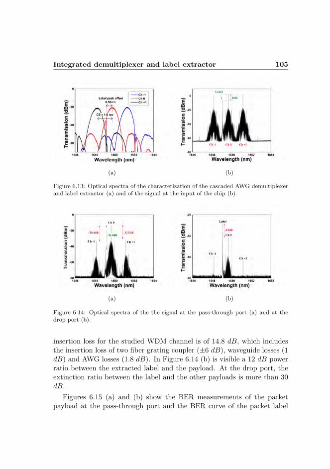
Integrated demultiplexer and label extractor 105
(a) (b)
Figure 6.13: Optical spectra of the characterization of the cascaded AWG demultiplexerand label extractor (a) and of the signal at the input of the chip (b).
(a) (b)
Figure 6.14: Optical spectra of the the signal at the pass-through port (a) and at thedrop port (b).
insertion loss for the studied WDM channel is of 14.8 dB, which includesthe insertion loss of two fiber grating coupler (±6 dB), waveguide losses (1dB) and AWG losses (1.8 dB). In Figure 6.14 (b) is visible a 12 dB powerratio between the extracted label and the payload. At the drop port, theextinction ratio between the label and the other payloads is more than 30dB.
Figures 6.15 (a) and (b) show the BER measurements of the packetpayload at the pass-through port and the BER curve of the packet label
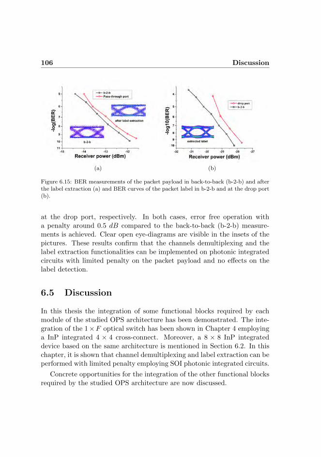
106 Discussion
(a) (b)
Figure 6.15: BER measurements of the packet payload in back-to-back (b-2-b) and afterthe label extraction (a) and BER curves of the packet label in b-2-b and at the drop port(b).
at the drop port, respectively. In both cases, error free operation witha penalty around 0.5 dB compared to the back-to-back (b-2-b) measure-ments is achieved. Clear open eye-diagrams are visible in the insets of thepictures. These results confirm that the channels demultiplexing and thelabel extraction functionalities can be implemented on photonic integratedcircuits with limited penalty on the packet payload and no effects on thelabel detection.
6.5 Discussion
In this thesis the integration of some functional blocks required by eachmodule of the studied OPS architecture has been demonstrated. The inte-gration of the 1×F optical switch has been shown in Chapter 4 employinga InP integrated 4 × 4 cross-connect. Moreover, a 8 × 8 InP integrateddevice based on the same architecture is mentioned in Section 6.2. In thischapter, it is shown that channel demultiplexing and label extraction can beperformed with limited penalty employing SOI photonic integrated circuits.
Concrete opportunities for the integration of the other functional blocksrequired by the studied OPS architecture are now discussed.
Discussion 107
6.5.1 Label detection
In this chapter the possible integration of the channels demultiplexing andthe label extraction functionalities has been demonstrated by employingtwo SOI integrated circuits.
The SOI platform allows the integration of of high-efficiency photodetec-tors and trans-impedance amplifiers. In [98] a photonic integrated devicewith Germanium photo-detectors and trans-impedance amplifiers (TIAs)on SOI is presented. Alternatively, heterogenous integration of high qual-ity III-V materials on top of SOI by means of molecular or adhesive bondingis possible. In [96], a 4-channel WDM demultiplexer with III-V photodiodesintegrated on SOI is presented.
A photonic integrated circuit with array waveguide gratings (AWGs),microring resonators (MRRs), photodetectors and CMOS amplifiers willallow the extraction, the detection and the amplification of the in-bandoptical labels considered in this work. Main requirements in such a deviceare high extinction ratio in the AWG to avoid channel crosstalk duringdemultiplexing and narrow band for the MRR-based filters to avoid payloaddistortions in the label extraction process.
SOI integrated microring resonators can be employed to implement alsothe bidirectional signals transmission required by the all-optical flow controldescribed in this thesis.
6.5.2 Label processor and switch controller
In the experiment presented in Chapter 4 the label processor and the switchcontroller have been implemented by using a dedicated label bits detectioncircuitry and a field-programmable gate array (FPGA) board. The cir-cuitry employed to detect the label bits is based on surface-mount device(SMD) components mounted on a printed circuit board (PCB). The PCBis connected to the digital pins of the FPGA board. The FPGA boardprocesses the detected label bits and, after contention resolution has beenperformed, drives the optical switch (including the wavelength selectors)according to the decoded label destinations.
The label processor and switch control requires limited computationalpower. The modular structure of the studied OPS architecture and theemployed labelling technique allow the parallel processing of each packet
108 Discussion
label. Moreover, each label bit can be processed in parallel.
CMOS technology, compatible with SOI photonic integrated circuits,can be employed to integrate the label processor and switch controller.The only limiting requirement of this control system is the large number ofrequired inputs/outputs. Many signals need to be processed in parallel andthe number of needed in/out pins is dependent on the switch port-count.
6.5.3 Fixed wavelength converter
In the experiment carried out in this thesis, wavelength conversion has beenperformed exploiting non-linear effects in semiconductor optical amplifiers(SOAs). Non-linear polarization rotation in a SOA has been used to convertthe WDM packets. High data-rate wavelength conversion employing thistechnique has been demonstrated [32].
Other non-linear effects in SOA, such as cross gain modulation (XGM) orcross phase modulation (XPM) for example, can be used to perform SOA-based wavelength conversion. The integration of the wavelength conversionfunctionality is possible. In [99], a fully InP monolithically integrated wave-length converter has been presented. This device combines a SOA and afast tunable multi-frequency laser, and error free operation at 40 Gb/s fordifferent wavelengths is demonstrated.
6.5.4 Conclusions
Photonic integration of a large port-count switch including all the requireddevices and functionalities on a single chip remains technologically demand-ing either for the fabrication and the electrical wiring.
In this thesis, two material platforms, namely SOI and InP, are consid-ered. Hybrid integration will allow to take advantage of the benefits pro-vided by the different material platforms. CMOS compatibility and limitedfootprint size of devices fabricated on SOI platform can be combined withthe opportunity of integrating active functionalities on III-V materials.
It is important to highlight that the photonic integrated circuits em-ployed in the experiments reported in this work have not been designedand fabricated specifically for the proposed optical packet switch architec-ture. Better results, in terms of total system losses could be achieved by
Summary 109
the design and the fabrication of dedicated photonic integrated circuits.
6.6 Summary
Further steps towards the total integration of the OPS architecture underinvestigation are taken in this chapter. The possible integration of the labelextractor is demonstrated. The performances of a SOI integrated labelextractor are investigated in a experimental set-up. The SOI chip consistsof an input port, four cascaded microring resonators, a pass-through portand four drop ports. The chip is tested injecting at its input a 160 Gb/sWDM payload coupled with three label wavelengths each of them carryingthree RF tone bits. The label bits can address up to 512 output ports. Thelabel wavelengths are successfully extracted by the microring resonators andcoupled out through the drop ports of the chip. Three label bits, associatedwith one of the label wavelengths, are then processed by a FPGA basedlabel processor and switch controller. The packet payload, after the labelfiltering process, is coupled out of the chip through the pass-through portand evaluated by a BERT. Dynamic label detection and processing is shownto operate correctly and error free operation of the system is shown with 1dB penalty on the packet payload.
In a second experiment presented in this chapter, the channel demulti-plexing functionality needed at each input of the studied OPS architectureis investigated in combination with the label extraction employing a SOI in-tegrated demultiplexer and label extractor. The employed SOI chip featuresa 1 × 32 AWG with 200 Ghz channel spacing that is used to demultiplex3 × 40 Gb/s WDM packet payloads. At the AWG input, a microring res-onator allows to implement the label extraction functionality on chip. Asingle label wavelength, inserted in the spectrum of one of the WDM pay-loads, is extracted by the microring based label extractor at the input of theAWG. BER measurements on the packet payload and the packet label areused to investigate the performance of the integrated packet demultiplexerand label extractor at the drop port and at the pass-through port of thechip, respectively. In both cases, error free operation is achieved with 0.5dB penalty compared to the back-to-back measurements, confirming thepossible integration of the demultiplexing and label extraction functionali-ties on a single device.
110 Summary
The integration of the other functionalities required by the proposedoptical packet switch architecture is discussed in this chapter. The totalOPS integration is still an open challenge. Scaling the OPS switch port-count, multiple devices and functionalities need to be integrated on thesame photonic device. Improvements in photonic integrated technologiesmay allow the fabrication of such large-scale photonic chip.
Chapter 7
Conclusions
The goal of this work was to identify, study and implement an opticalpacket switch architecture for high performance data center networks. Sucha switch is required to handle a large number of high data-rate ports toenhance the resources sharing capabilities in these systems. Also, it shouldadd negligible latency to the system to improve the system performance.
A novel single-chain model that allows computing a multi-port systemthroughput and latency as function of the employed switch architectureand as function of the switch port-count is used as a tool to identify a suit-able architecture. This study highlights the need of a distributed control toobtain low switch reconfiguration time, while scaling to a large port-count.As a result, a novel architecture is presented. It is a modular strictly non-blocking architecture. Wavelength division multiplexing is used to scalethe switch port-count. The total number of inputs/outputs is given by thenumber of input fibers F multiplied by the number of wavelength channelscarried by each fiber M . Wavelength conversion is used to partially solvepacket contention “on the fly” in the optical domain. Also, it allows par-allel and autonomous operations of the architecture modules. Flow controlfunctionality is provided in case packet contentions cannot be solved in theoptical domain. The modular structure of the novel architecture and theparallel modules operations enable the employment of highly distributedcontrol, which in turn allows for port-count independent nanosecond-scaleswitch reconfiguration time.
The performances of the novel architecture in a data center scenario are
112
investigated by means of simulations. The architecture is shown to handlesynchronous and asynchronous traffic providing sub-microsecond averageend-to-end latency, low packet loss and high throughput under relativelyhigh traffic load and using a limited buffer capacity. The simulations resultsin terms of throughput are in agreement with the ones obtained by apply-ing the single-chain model, while discrepancies are evident for the latencyresults. This is due to the fact that the model does not consider the buffercapacity that strongly affects the system latency. The effects of the buffercapacity on the system performances are investigated with an interestingresult. Under heavy traffic conditions, increasing the buffer capacity doesnot improve the performance of the system in terms of packet loss, resultingalso in increased system latency due to longer queueing times.
The architecture module subsystem is implemented for the first time inexperimental set-up, not considering the flow control functionality. Thefeasibility of a 64 × 64 optical switch based on the novel architecture isdemonstrated by testing the dynamic switching capabilities of a 1× 8 sub-system based on discrete optical components. The integration of the 1×Foptical switch required by each architecture module is exploited employ-ing a 1 × 4 InP integrated optical cross-connect. 4 parallel chips like theone employed would allow the implementation of a 16 × 16 optical packetswitch. The two subsystems are studied injecting 8 (4) WDM channels at40 Gb/s. Each 1 × 8 (1 × 4) module can provide 320 Gb/s (160 Gb/s) ofmaximum throughput. This translates in a maximum throughput of over2.5 Tb/s (640 Gb/s) considering a 64 × 64 (16 × 16) switch based on thenovel architecture. The radio frequency tone in-band label detection, afterlabel extraction, is performed by a dedicated printed circuit board basedon pass-band filters and envelope detectors. The label processor, the switchcontroller, the contention resolution functionality and the wavelength se-lector controller are implemented by programming an FPGA. In both casesstudied, the switch subsystem configuration takes place in only 25 ns dueto the employed parallel labelling and label processing techniques, regard-less the number of label wavelengths and tones employed to encode thepacket address. This result confirms that the switch configuration time isport-count independent. This is a remarkable result, since this time delayincludes the time it takes to extract and process the labels, to solve thecontentions and to drive the 1× 8 (or 1× 4) optical switch. Moreover, dueto the parallel and autonomous operations of the switch modules, this is
113
the time to configure the whole switch architecture. The configuration timecan be further reduced simply employing a faster FPGA, since 10 ns outof the total 25 ns are due to the single clock-cycle (100 MHz) required bythe FPGA to perform its functionalities.
The flow control functionality is investigated by employing two distinctimplementations. A FPGA-based implementation is tested successfully ina experimental set-up. Contended packets are correctly retransmitted andthe round robin algorithm employed as priority policy ensures balancedbuffer utilization. This implementation would require a dedicated electri-cal network, solution that is not practical in a large-scale system as a DCnetwork. As a consequence, an all-optical implementation is considered.To reduce the number of required optical transmitters, part of the opticalpower of the extracted in-band label is employed to generate an opticalacknowledge message. A semiconductor optical amplifier driven by theswitch controller is used as modulator to generate the optical acknowledg-ment. This signal is sent back employing the same optical path used for thepacket transmission. An extra receiver is needed at the transmitting nodeto detect the optical acknowledgement. However, no extra optical links arerequired.
The integration of some of the functional blocks required by the proposedoptical switch architecture is demonstrated in this work. Integration of theoptical switch, label extractor and channels demultiplexer is experimentallyinvestigated by using photonic integrated circuits. Channels demultiplexingand labels extraction functionalities are demonstrated by employing SOIintegrated chips. Error free operations on the packet payload and the packetlabels with 0.5 dB penalty is demonstrated. Also, the integration of theother functionalities required by a single architecture module is discussed.
Port-count scalability
The port-count scalability of the proposed architecture needs be to dis-cussed considering two main aspects: the control and the practical imple-mentation.
From a control point of view the port-count does not represent a prob-lem. The employed radio frequency in-band labelling technique allows ad-dressing a large number of ports. In this work, it has been shown that
114
512 distinct destinations can be addressed employing 3 label wavelengthseach of them carrying 3 tones. If a larger number of ports needs to be ad-dressed more tones can be encoded in each label wavelength or more labelwavelengths can be inserted in the signal spectrum, without affecting thepacket payload. The limits of this technique have been presented in [84].Moreover, the modular structure of the architecture in combination withthe parallel label processing employed allows the switch configuration timeto be port-count independent.
Different considerations can be given about the optical switch implemen-tation. Basically, the port-count scalability of the architecture is limitedby the splitting losses of the broadcast stage of the optical switch requiredin each module. As already discussed in Section 4.4, wavelength divisionmultiplexing is the key to scale the proposed architecture to a large port-count. However, as the number of wavelength channels transmitted in asingle fiber increases, high extinction ratio and low cross-talk AWGs arerequired on chip. Nonlinear effects in semiconductor optical amplifiers andoptical signal-to-noise degradation have also to be considered.
Latency
Main advantage of the novel architecture is that the overall switch con-figuration time is reduced to the time needed to extract and process apacket label (all labels can be extracted and processed in parallel and au-tonomously), to solve the contentions in a single M ×1 wavelength selectorand to drive a single 1×F optical switch. This leads to a promising result:25 ns are required to carry out all the needed operations, regardless thenumber of employed label wavelengths and radio frequency tones. Parallellabel bits detection performed by the dedicated electronic circuitry takes15 ns, while label decoding, contention resolution and switch control areperformed by the employed FPGA in only 1 clock-cycle (10 ns). Alter-native implementations of the label bit detection circuitry may lower therequired processing delay. In addition, the employment of an FPGA witha faster processor will further reduce the control time. However, the packetlatency may result in considerably larger time due to possible contentionsand subsequent packet retransmission. Since the buffering is performedat the edges of the switching matrix the total system latency is strongly
115
dependent on the system round trip time and thus on the host-switch dis-tance. Positioning the electrical buffers and the optical transceivers as closeas possible to the optical switch would mitigate this limitation.
Data-rate
The maximum data-rate that can be employed is limited by two functionalblocks of the proposed architecture. The optical switch maximum data-rate depends on the wavelength selective stage pass-band. For example,the employed 1 × 4 has a 3-dB bandwidth greater than 100 GHz [100].This switching module is data-format agnostic. However, in this contextit is the SOA-based wavelength conversion that limits the operation tointensity-modulated signals. The employment of optoelectronic wavelengthconverters will solve this issue.
Throughput
Employing a centralized large port-count optical packet switch at the clus-ter layer of the data center architecture would enhance the resource sharingbetween the servers of a datacenter. In this scenario, all the cluster of thedata center have equal available bandwidth and equal logical distance fromeach other. This will allow to spread the workload between the massivehardware equipment available in a DC network in a balanced manner. Intheory, a perfect balanced traffic in a system employing the proposed ar-chitecture will allow to reach 100% of bandwidth utilization, i.e. maximumthroughput.
Integration
In this thesis the possible integration of the required 1× F optical switch,the channel demultiplexer and the label extractor has been demonstrated.
It is important to remark that the employed photonic integrated circuitshave not been designed and fabricated specifically for the proposed archi-tecture. Available chips have been used to demonstrate that it is possibleto integrate the functional blocks required by the novel architecture. Chips

116
with a dedicated design would allow better results in terms of total sys-tem losses and chip footprint size, reducing both fabrication and operationcosts.
The SOI platform also allows the integration on the same chip employedas label extractor of high-efficiency photo-detectors and trans-impedanceamplifiers that can be used to detect and amplify the packet labels beforethe required processing. The integration of SOA-based wavelength convert-ers is also feasible.
To take advantage of both material platforms investigated, namely SOIand InP, an hybrid integration of the required switch functional blocksseems to be the optimal solution.
The simplicity and the limited computational requirements of the em-ployed control system (label processor and switch controller) allow easilyintegration of the architecture control. The basic limitation is the numberof required input/output pins to process all signals in parallel, number thatdepends on the switch port-count.
Power consumption
Due to the early stage of the switch architecture implementation, few con-siderations can be made about the power consumption. For example, the1×4 integrated optical cross-connect employed in this work has been shownto consume 3 pJ/bit while routing 40 Gb/s signals (not considering thepower supply and the temperature controller) [100]. In the system level ex-periments carried out in this thesis, this value is significantly increased bythe switch controller. Consider that only the employed FPGA developmentboard consumes 25 W . A fair power consumption analysis would requirean experimental set-up employing integrated electronic and optical compo-nents specifically designed for the proposed architecture. It can be said thatscaling the switch port-count will correspond to increased power consump-tions due to the higher driven current required to bias longer semiconduc-tor optical amplifiers. However, the power consumption is not data-ratedependent, thus higher power efficiency can be achieved by using higherdata-rate.
117
Alternative approaches
The approach employed in this thesis to design a high performance datacenter network is to employ a centralized, large port-count optical packetswitch at the cluster level of the network. Such a switch, employing WDM,could guarantee the large port-count and high communication bandwidthrequired in the cluster interaction process, while providing low transmis-sion latency due to its modular structure and distributed control system.Moreover, the proposed data center network could benefit of an enhancedresource sharing and would allow the opportunity of spreading the serversworkload in a balanced manner.
Due to the bimodal distribution of the data center traffic, hybrid electrical-optical solutions have been considered [101–103]. Basically, the data centertraffic consists of short lived flows (small control packets) and long livedflows (fragmented portions of large files). The hybrid approach relies onthe employment of standard electronic packet switches to handle the shortlived flows and optical circuit switches to forward the long lived flows totheir destination. A parallel optical network is then available in case largebandwidth is required in the inter-rack or inter-cluster communication pro-cess. However, this approach needs traffic control and provisioning whichis rather difficult in a data center environment and may lead to undesiredsystem latency and reduced throughput.
An all-optical solution in which both packet and circuit switching areperformed by two parallel optical networks represents the best solution toface the increasing bandwidth requirements of the data center networks, asconfirmed by recent projects such as [104]. The proposed optical packetswitch is suited for this hybrid implementation.
The study of optical packet switching reported in this thesis is focusedon the physical implementation of an optical packet switch and its con-troller. The data center network management has not been considered.In this contest, the employment of software-defined networking (SDN) isof continuously increasing interest [105–107]. It consists in decoupling thecontrol plane, where the routing decisions are made, and the data plane ofthe network, where the packets are effectively forwarded. The control planeis directly programmable and a more sophisticated traffic management isenabled by the physical separation from the forwarding plane. The controlis centralized in software-based controllers that can control or modify the
118
flow table of network devices (physical or virtual) through a standard inter-face, OpenFlow is the dominant protocol [108]. In the contest of this thesis,SDN could be used to control, redirect and balance the traffic flows of theToR and cluster switches maximizing the throughput of the centralizedoptical packet switch.
Recommendations
The implementation of the novel optical packet switch architecture de-scribed and studied in this thesis is still in its infancy. This work showspromising results towards the fabrication of a fast large port-count inte-grated optical packet switch for high performance data center networks.However, the realization of a prototype that can be tested in a real datacenter environment requires further research. The design and fabricationof dedicated photonic integrated circuits will allow to exploit the real po-tentialities of the novel architecture.
The experiments results presented in this work are obtained consideringsynchronous traffic, considering packets with fixed size. Testing the switcharchitecture under asynchronous operations, considering variable packetsize would require enhanced functionalities in the switch controller and inthe contentions solving process. This may affect the control complexityand, as a consequence, the system latency.

Bibliography
[1] “Broadcast yourself.” http://www.youtube.com/.
[2] “Connect with friends and the world around you on facebook.” http://www.facebook.com.
[3] “The fastest, simplest way to stay close to everything you care about.”https://twitter.com/about.
[4] “Everything you need, everywhere you go.” http://www.google.com/drive/about.html.
[5] M. Meeker and L. Wu, “2013 internet trends,” Kleiner Perkins Cau-field & Byers, Tech. Rep., May 2013.
[6] T. Koonen, “Fiber to the home/fiber to the premises: what, where,and when?” Proceedings of the IEEE, vol. 94, no. 5, pp. 911–934,2006.
[7] Cisco, “Cisco global cloud index: Forecast and methodology, 20112016,” http://www.cisco.com/en/US/solutions/collateral/ns341/ns525/ns537/ns705/ns1175/Cloud Index White Paper.pdf, Tech.Rep., 2012.
[8] S. Sakr, A. Liu, D. M. Batista, and M. Alomari, “A survey of largescale data management approaches in cloud environments,” Commu-nications Surveys & Tutorials, IEEE, vol. 13, no. 3, pp. 311–336,2011.
[9] L. A. Barroso and U. Holzle, “The datacenter as a computer: Anintroduction to the design of warehouse-scale machines,” SynthesisLectures on Computer Architecture, vol. 4, no. 1, pp. 1–108, 2009.
[10] R. Brown et al., “Report to congress on server and data center energyefficiency: Public law 109-431,” 2008.
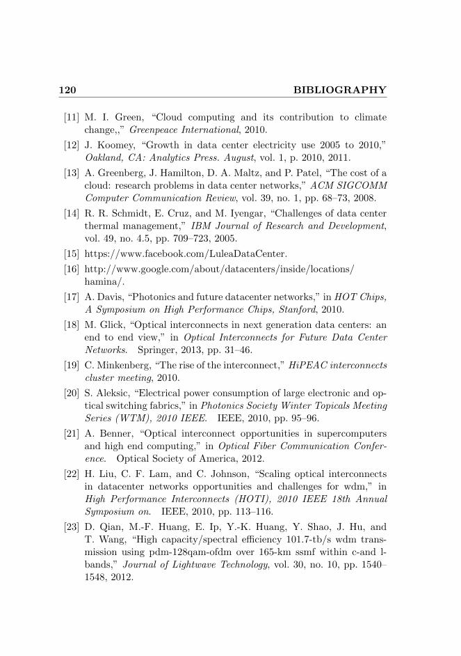
120 BIBLIOGRAPHY
[11] M. I. Green, “Cloud computing and its contribution to climatechange,,” Greenpeace International, 2010.
[12] J. Koomey, “Growth in data center electricity use 2005 to 2010,”Oakland, CA: Analytics Press. August, vol. 1, p. 2010, 2011.
[13] A. Greenberg, J. Hamilton, D. A. Maltz, and P. Patel, “The cost of acloud: research problems in data center networks,” ACM SIGCOMMComputer Communication Review, vol. 39, no. 1, pp. 68–73, 2008.
[14] R. R. Schmidt, E. Cruz, and M. Iyengar, “Challenges of data centerthermal management,” IBM Journal of Research and Development,vol. 49, no. 4.5, pp. 709–723, 2005.
[15] https://www.facebook.com/LuleaDataCenter.
[16] http://www.google.com/about/datacenters/inside/locations/hamina/.
[17] A. Davis, “Photonics and future datacenter networks,” in HOT Chips,A Symposium on High Performance Chips, Stanford, 2010.
[18] M. Glick, “Optical interconnects in next generation data centers: anend to end view,” in Optical Interconnects for Future Data CenterNetworks. Springer, 2013, pp. 31–46.
[19] C. Minkenberg, “The rise of the interconnect,” HiPEAC interconnectscluster meeting, 2010.
[20] S. Aleksic, “Electrical power consumption of large electronic and op-tical switching fabrics,” in Photonics Society Winter Topicals MeetingSeries (WTM), 2010 IEEE. IEEE, 2010, pp. 95–96.
[21] A. Benner, “Optical interconnect opportunities in supercomputersand high end computing,” in Optical Fiber Communication Confer-ence. Optical Society of America, 2012.
[22] H. Liu, C. F. Lam, and C. Johnson, “Scaling optical interconnectsin datacenter networks opportunities and challenges for wdm,” inHigh Performance Interconnects (HOTI), 2010 IEEE 18th AnnualSymposium on. IEEE, 2010, pp. 113–116.
[23] D. Qian, M.-F. Huang, E. Ip, Y.-K. Huang, Y. Shao, J. Hu, andT. Wang, “High capacity/spectral efficiency 101.7-tb/s wdm trans-mission using pdm-128qam-ofdm over 165-km ssmf within c-and l-bands,” Journal of Lightwave Technology, vol. 30, no. 10, pp. 1540–1548, 2012.
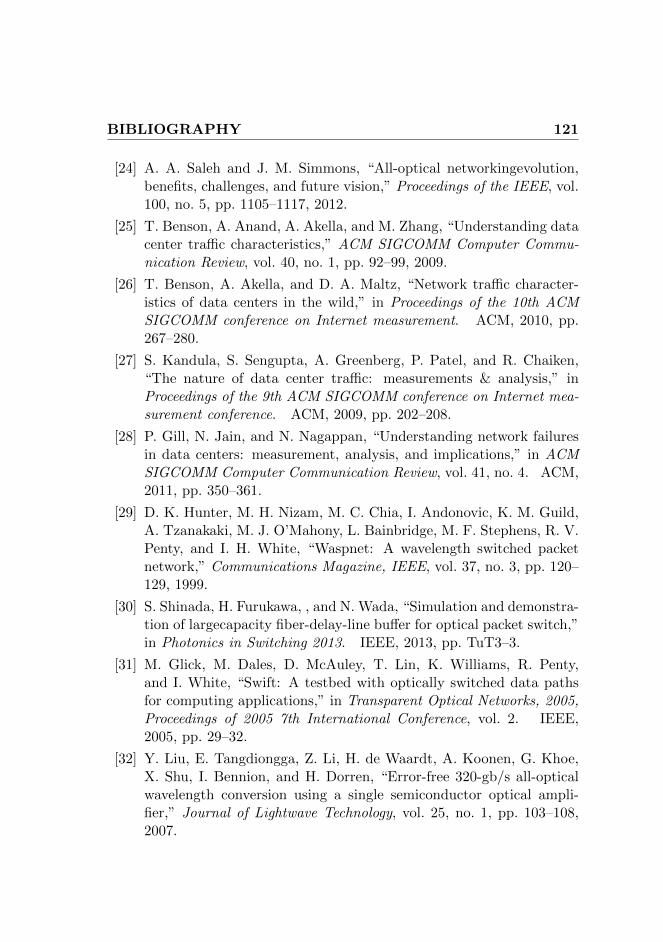
BIBLIOGRAPHY 121
[24] A. A. Saleh and J. M. Simmons, “All-optical networkingevolution,benefits, challenges, and future vision,” Proceedings of the IEEE, vol.100, no. 5, pp. 1105–1117, 2012.
[25] T. Benson, A. Anand, A. Akella, and M. Zhang, “Understanding datacenter traffic characteristics,” ACM SIGCOMM Computer Commu-nication Review, vol. 40, no. 1, pp. 92–99, 2009.
[26] T. Benson, A. Akella, and D. A. Maltz, “Network traffic character-istics of data centers in the wild,” in Proceedings of the 10th ACMSIGCOMM conference on Internet measurement. ACM, 2010, pp.267–280.
[27] S. Kandula, S. Sengupta, A. Greenberg, P. Patel, and R. Chaiken,“The nature of data center traffic: measurements & analysis,” inProceedings of the 9th ACM SIGCOMM conference on Internet mea-surement conference. ACM, 2009, pp. 202–208.
[28] P. Gill, N. Jain, and N. Nagappan, “Understanding network failuresin data centers: measurement, analysis, and implications,” in ACMSIGCOMM Computer Communication Review, vol. 41, no. 4. ACM,2011, pp. 350–361.
[29] D. K. Hunter, M. H. Nizam, M. C. Chia, I. Andonovic, K. M. Guild,A. Tzanakaki, M. J. O’Mahony, L. Bainbridge, M. F. Stephens, R. V.Penty, and I. H. White, “Waspnet: A wavelength switched packetnetwork,” Communications Magazine, IEEE, vol. 37, no. 3, pp. 120–129, 1999.
[30] S. Shinada, H. Furukawa, , and N. Wada, “Simulation and demonstra-tion of largecapacity fiber-delay-line buffer for optical packet switch,”in Photonics in Switching 2013. IEEE, 2013, pp. TuT3–3.
[31] M. Glick, M. Dales, D. McAuley, T. Lin, K. Williams, R. Penty,and I. White, “Swift: A testbed with optically switched data pathsfor computing applications,” in Transparent Optical Networks, 2005,Proceedings of 2005 7th International Conference, vol. 2. IEEE,2005, pp. 29–32.
[32] Y. Liu, E. Tangdiongga, Z. Li, H. de Waardt, A. Koonen, G. Khoe,X. Shu, I. Bennion, and H. Dorren, “Error-free 320-gb/s all-opticalwavelength conversion using a single semiconductor optical ampli-fier,” Journal of Lightwave Technology, vol. 25, no. 1, pp. 103–108,2007.
122 BIBLIOGRAPHY
[33] M. Smit, X. Leijtens, E. Bente, J. van der Tol, H. Ambrosius, D. Rob-bins, M. Wale, N. Grote, and M. Schell, “A generic foundry model forinp-based photonic ics,” in Optical Fiber Communication Conferenceand Exposition (OFC/NFOEC), 2012 and the National Fiber OpticEngineers Conference. IEEE, 2012, pp. 1–3.
[34] X. Leijtens, “Jeppix: the platform for indium phosphide-based pho-tonics,” Optoelectronics, IET, vol. 5, no. 5, pp. 202–206, 2011.
[35] P. Dumon, W. Bogaerts, R. Baets, J.-M. Fedeli, and L. Fulbert, “To-wards foundry approach for silicon photonics: silicon photonics plat-form epixfab,” Electronics letters, vol. 45, no. 12, pp. 581–582, 2009.
[36] R. Nagarajan, M. Kato, J. Pleumeekers, P. Evans, S. Corzine,S. Hurtt, A. Dentai, S. Murthy, M. Missey, R. Muthiah et al., “Inpphotonic integrated circuits,” Selected Topics in Quantum Electron-ics, IEEE Journal of, vol. 16, no. 5, pp. 1113–1125, 2010.
[37] A. Kaneko, T. Goh, H. Yamada, T. Tanaka, and I. Ogawa, “Designand applications of silica-based planar lightwave circuits,” SelectedTopics in Quantum Electronics, IEEE Journal of, vol. 5, no. 5, pp.1227–1236, 1999.
[38] R. Soref, “The past, present, and future of silicon photonics,” SelectedTopics in Quantum Electronics, IEEE Journal of, vol. 12, no. 6, pp.1678–1687, 2006.
[39] Y. Hibino, “Recent advances in high-density and large-scale awgmulti/demultiplexers with higher index-contrast silica-based plcs,”Selected Topics in Quantum Electronics, IEEE Journal of, vol. 8,no. 6, pp. 1090–1101, 2002.
[40] Y. Hibino, Y. Hida, A. Kaneko, M. Ishii, M. Itoh, T. Goh, A. Sugita,T. Saida, A. Himeno, and Y. Ohmori, “Fabrication of silica-on-siwaveguide with higher index difference and its application to 256channel arrayed waveguide multi/demultiplexer,” in Optical FiberCommunication Conference, 2000, vol. 2. IEEE, 2000, pp. 127–129.
[41] P. Doussiere, “High power lasers on inp substrates,” in PhotonicsConference (PHO), 2011 IEEE. IEEE, 2011, pp. 674–675.
[42] K. Prosyk, T. Brast, M. Gruner, M. Hamacher, D. Hoffmann, R. Mil-lett, and K.-O. Velthaus, “Tunable inp-based optical iq modulator for160 gb/s,” in European Conference and Exposition on Optical Com-
BIBLIOGRAPHY 123
munications. Optical Society of America, 2011.
[43] L. Rowe, M. Elsey, N. Tarr, A. Knights, and E. Post, “Cmos-compatible optical rib waveguides defined by local oxidation of sil-icon,” Electronics Letters, vol. 43, no. 7, pp. 392–393, 2007.
[44] T. Mitze, M. Schnarrenberger, L. Zimmermann, J. Bruns, F. Fidorra,J. Kreissl, K. Janiak, S. Fidorra, H. Heidrich, and K. Petermann,“Hybrid integration of iii/v lasers on a silicon-on-insulator (soi) op-tical board,” in Group IV Photonics, 2005. 2nd IEEE InternationalConference on. IEEE, 2005, pp. 210–212.
[45] H. Park, A. W. Fang, S. Kodama, and J. E. Bowers, “Hybrid siliconevanescent laser fabricated with a silicon waveguide and iii-v offsetquantum well,” 2005.
[46] H. Park, A. W. Fang, O. Cohen, R. Jones, M. J. Paniccia, and J. E.Bowers, “A hybrid algainas–silicon evanescent amplifier,” PhotonicsTechnology Letters, IEEE, vol. 19, no. 4, pp. 230–232, 2007.
[47] A. W. Fang, H. Park, O. Cohen, R. Jones, M. J. Paniccia, andJ. E. Bowers, “Electrically pumped hybrid algainas-silicon evanescentlaser,” Opt. Express, vol. 14, no. 20, pp. 9203–9210, 2006.
[48] E. Yamada, S. Kanazawa, A. Ohki, K. Watanabe, Y. Nasu,N. Kikuchi, Y. Shibata, R. Iga, and H. Ishii, “112-gb/s inp dp-qpskmodulator integrated with a silica-plc polarization multiplexing cir-cuit,” in Optical Fiber Communication Conference and Exposition(OFC/NFOEC), 2012 and the National Fiber Optic Engineers Con-ference. IEEE, 2012, pp. 1–3.
[49] V. Aksyuk, S. Arney, N. Basavanhally, D. Bishop, C. Bolle, C. Chang,R. Frahm, A. Gasparyan, J. Gates, R. George et al., “238 x 238 mi-cromechanical optical cross connect,” Photonics Technology Letters,IEEE, vol. 15, no. 4, pp. 587–589, 2003.
[50] N. Xie, T. Hashimoto, and K. Utaka, “Ultimate-low-power-consumption, polarization-independent, and high-speed poly-mer mach-zehnder thermo-optic switch,” in Optical FiberCommunication-incudes post deadline papers, 2009. OFC 2009.Conference on. IEEE, 2009, pp. 1–3.
[51] R. Luijten, W. E. Denzel, R. R. Grzybowski, and R. Hemenway, “Op-tical interconnection networks: The osmosis project,” in Lasers and
124 BIBLIOGRAPHY
Electro-Optics Society, 2004. LEOS 2004. The 17th Annual Meetingof the IEEE, vol. 2. IEEE, 2004, pp. 563–564.
[52] H. Wang, A. Wonfor, K. Williams, R. Penty, and I. White, “Demon-stration of a lossless monolithic 16 x16 qw soa switch,” in OpticalCommunication, 2009. ECOC’09. 35th European Conference on, vol.2009. IEEE, 2009, pp. 1–2.
[53] S. C. Nicholes, M. L. Masanovic, B. Jevremovic, E. Lively, L. A.Coldren, and D. J. Blumenthal, “The worlds first inp 8x8 monolithictunable optical router (motor) operating at 40 gbps line rate perport,” in National Fiber Optic Engineers Conference. Optical Societyof America, 2009.
[54] I. M. Soganci, T. Tanemura, K. Williams, N. Calabretta, T. de Vries,E. Smalbrugge, M. Smit, H. Dorren, and Y. Nakano, “Integratedphased-array 1× 16 photonic switch for wdm optical packet switchingapplication,” in Photonics in Switching, 2009. PS’09. InternationalConference on. IEEE, 2009, pp. 1–2.
[55] N. Calabretta, I. M. Soganci, T. Tanemura, W. Wang, O. Raz,K. Higuchi, K. A. Williams, T. de Vries, Y. Nakano, and H. Dorren,“1× 16 optical packet switch sub-system with a monolithically inte-grated inp optical switch,” in Optical Fiber Communication (OFC),collocated National Fiber Optic Engineers Conference, 2010 Confer-ence on (OFC/NFOEC). IEEE, 2010, pp. 1–3.
[56] I. M. Soganci, T. Tanemura, K. Takeda, M. Zaitsu, M. Takenaka,and Y. Nakano, “Monolithic inp 100-port photonic switch,” in Op-tical Communication (ECOC), 2010 36th European Conference andExhibition on. IEEE, 2010, pp. 1–3.
[57] J. Gripp, M. Duelk, J. Simsarian, A. Bhardwaj, P. Bernasconi,O. Laznicka, and M. Zirngibl, “Optical switch fabrics for ultra-high-capacity ip routers,” Lightwave Technology, Journal of, vol. 21, no. 11,pp. 2839–2850, 2003.
[58] A. Shacham, B. Small, O. Liboiron-Ladouceur, and K. Bergman, “Afully implemented 12 times; 12 data vortex optical packet switchinginterconnection network,” Lightwave Technology, Journal of, vol. 23,no. 10, pp. 3066–3075, 2005.
[59] A. Shacham and K. Bergman, “Building ultralow-latency intercon-nection networks using photonic integration,” Micro, IEEE, vol. 27,
BIBLIOGRAPHY 125
no. 4, pp. 6–20, 2007.
[60] C. Kachris and I. Tomkos, “A survey on optical interconnects for datacenters,” 2012.
[61] S. Di Lucente, N. Calabretta, J. Resing, and H. Dorren, “Scalinglow-latency optical packet switches to a thousand ports,” Journal ofOptical Communications and Networking, vol. 4, no. 9, pp. A17–A28,2012.
[62] D. Opferman and N. Tsao-Wu, “On a class of rearrangeable switchingnetworks,” Bell Syst. Tech. J, vol. 50, no. 5, pp. 1579–1618, 1971.
[63] S. Andresen, “The looping algorithm extended to base 2t rearrange-able switching networks,” Communications, IEEE Transactions on,vol. 25, no. 10, pp. 1057–1063, 1977.
[64] K. Y. Lee, “A new benes network control algorithm,” Computers,IEEE Transactions on, vol. 100, no. 6, pp. 768–772, 1987.
[65] T. T. Lee and S.-Y. Liew, “Parallel routing algorithms in benes-closnetworks,” in INFOCOM’96. Fifteenth Annual Joint Conference ofthe IEEE Computer Societies. Networking the Next Generation. Pro-ceedings IEEE, vol. 1. IEEE, 1996, pp. 279–286.
[66] N. A. Shalmany and A. Rahbar, “On the choice of all-optical switchesfor optical networking,” in High Capacity Optical Networks and En-abling Technologies, 2007. HONET 2007. International Symposiumon. IEEE, 2007, pp. 1–8.
[67] R. Spanke, “Architectures for large nonblocking optical spaceswitches,” Quantum Electronics, IEEE Journal of, vol. 22, no. 6, pp.964–967, 1986.
[68] N. Calabretta, W. Wang, T. Ditewig, O. Raz, F. G. Agis, S. Z. H.de Waardt, and H. Dorren, “Scalable optical packet switches for mul-tiple data formats and data rates packets,” Photonics Technology Let-ters, IEEE, vol. 22, no. 7, pp. 483–485, 2010.
[69] W. Wang, N. Calabretta, T. Ditewig, F. G. Agis, S. Zhang, O. Raz,E. Tangdiongga, and H. Dorren, “Scalable optical packet switchingat 160 gb/s data rate,” in Optical Communication, 2009. ECOC’09.35th European Conference on. IEEE, 2009, pp. 1–2.
[70] R. Hemenway, R. Grzybowski, C. Minkenberg, and R. Luijten,“Optical-packet-switched interconnect for supercomputer applica-
126 BIBLIOGRAPHY
tions [invited],” Journal of Optical Networking, vol. 3, no. 12, pp.900–913, 2004.
[71] M. Batayneh, D. A. Schupke, M. Hoffmann, A. Kirstaedter, andB. Mukherjee, “On routing and transmission-range determination ofmulti-bit-rate signals over mixed-line-rate wdm optical networks forcarrier ethernet,” IEEE/ACM Transactions on Networking (TON),vol. 19, no. 5, pp. 1304–1316, 2011.
[72] M. Batayneh, D. Schupke, M. Hoffmann, A. Kirstaedter, andB. Mukherjee, “Reliable multi-bit-rate vpn provisioning for multi-point carrier-grade ethernet services over mixed-line-rate wdm opti-cal networks,” Optical Communications and Networking, IEEE/OSAJournal of, vol. 3, no. 1, pp. 66–76, 2011.
[73] N. Kikuchi, Y. Shibata, H. Okamoto, Y. Kawaguchi, S. Oku,Y. Kondo, and Y. Tohmori, “Monolithically integrated 100-channelwdm channel selector employing low-crosstalk awg,” Photonics Tech-nology Letters, IEEE, vol. 16, no. 11, pp. 2481–2483, 2004.
[74] http://www.omnetpp.org/.
[75] S. Di Lucente, R. Pueyo Centelles, H. J. Dorren, and N. Calabretta,“Study of the performance of an optical packet switch architecturewith highly distributed control in a data center environment,” in Op-tical Network Design and Modeling (ONDM), 2012 16th InternationalConference on. IEEE, 2012, pp. 1–6.
[76] N. Calabretta, R. P. Centelles, S. D. Lucente, and H. J. S. Dorren,“On the performance of a large-scale optical packet switch under re-alistic data center traffic,” Journal of Optical Communication andNetworking, vol. 5, no. 6, pp. 565–573, 2013.
[77] N. Beheshti, Y. Ganjali, M. Ghobadi, N. McKeown, and G. Salmon,“Experimental study of router buffer sizing,” in Proceedings of the8th ACM SIGCOMM conference on Internet measurement. ACM,2008, pp. 197–210.
[78] N. Beheshti, Y. Ganjali, R. Rajaduray, D. Blumenthal, and N. McK-eown, “Buffer sizing in all-optical packet switches,” in Optical FiberCommunication Conference. Optical Society of America, 2006.
[79] R. Sinha, C. Papadopoulos, and J. Heidemann, “Internet packet sizedistributions: Some observations,” USC/Information Sciences Insti-
BIBLIOGRAPHY 127
tute [Online], year=2007.
[80] CAIDA, “Packet size distribution comparison between internet linksin 1998 and 2008,” http://www.caida.org/research/traffic-analysis/pkt size distribution/graphs.xml, 2008.
[81] J. Luo, S. Di Lucente, J. Ramirez, H. J. Dorren, and N. Calabretta,“Low latency and large port count optical packet switch with highlydistributed control,” in Optical Fiber Communication Conference.Optical Society of America, 2012.
[82] S. Di Lucente, J. Luo, A. Rohit, S. Zou, K. A. Williams, H. Dorren,and N. Calabretta, “Fpga controlled integrated optical cross-connectmodule for high port-density optical packet switch,” in European Con-ference and Exhibition on Optical Communication. Optical Societyof America, 2012.
[83] S. Di Lucente, J. Luo, R. P. Centelles, A. Rohit, S. Zou, K. Williams,H. Dorren, and N. Calabretta, “Numerical and experimental study ofa high port-density wdm optical packet switch architecture for datacenters,” Optics express, vol. 21, no. 1, pp. 263–269, 2013.
[84] J. Luo, H. J. Dorren, and N. Calabretta, “Optical rf tone in-band la-beling for large-scale and low-latency optical packet switches,” Light-wave Technology, Journal of, vol. 30, no. 16, pp. 2637–2645, 2012.
[85] M. Matsuura, N. Kishi, and T. Miki, “Ultra-wideband wavelengthconversion over 300 nm by cascaded soa-based wavelength convert-ers,” in Proc. OFC/NFOEC, 2006, pp. 1–3.
[86] A. Rohit, A. Albores-Mejia, J. Bolk, X. Leijtens, and K. Williams,“Multi-path routing in an monolithically integrated 4x4 broadcastand select wdm cross-connect,” in European Conference and Exposi-tion on Optical Communications. Optical Society of America, 2011.
[87] M. Renaud, M. Bachmann, and M. Erman, “Semiconductor opticalspace switches,” Selected Topics in Quantum Electronics, IEEE Jour-nal of, vol. 2, no. 2, pp. 277–288, 1996.
[88] M. Gustavsson, B. Lagerstrom, L. Thylen, M. Janson, L. Lundgren,A.-C. Morner, M. Rask, and B. Stoltz, “Monolithically integrated 4×4 ingaasp/inp laser amplifier gate switch arrays,” Electronics Letters,vol. 28, no. 24, pp. 2223–2225, 1992.
[89] E. Aw, A. Wonfor, M. Glick, R. Penty, and I. White, “An optimized
128 BIBLIOGRAPHY
non-blocking soa switch architecture for high performance tb/s net-work interconnects,” in Photonics in Switching, 2007. IEEE, 2007,pp. 15–16.
[90] S. D. Lucente, J. Luo, A. Rohit, K. Williams, H. Dorren, and N. Cal-abretta, “Optical packet switch node with packet flow control for flatinter-cluster data center network,” in Optical Fiber CommunicationConference/National Fiber Optic Engineers Conference 2013. Opti-cal Society of America, 2013, p. OW3H.4.
[91] W. Miao, S. Di Lucente, J. Luo, H. Dorren, and N. Calabretta, “Lowlatency and efficient optical flow control for intra data center net-works,” in European Conference and Exhibition on Optical Commu-nication. Optical Society of America, 2013.
[92] S. Di Lucente, P. De Heyn, J. Luo, D. Van Thourhout, H. Dorren, andN. Calabretta, “160 gb/s optical packet switch module employing soiintegrated label extractor,” in Photonics in Switching 2013. IEEE,2013, pp. TuT3–1.
[93] P. De Heyn, J. Luo, A. Trita, S. Pathak, S. Di Lucente, H. Dorren,N. Calabretta, and D. Van Thourhout, “A compact integrated 40gb/spacket demultiplexer and label extractor on silicon-on-insulator foran optical packet switch,” in European Conference and Exhibition onOptical Communication. Optical Society of America, 2013.
[94] A. Rohit, R. Stabile, and K. A. Williams, “8× 8 space and wavelengthselective cross-connect for simultaneous dynamic multi-wavelengthrouting,” in Optical Fiber Communication Conference. Optical So-ciety of America, 2013.
[95] P. De Heyn, D. Vermeulen, T. Van Vaerenbergh, B. Kuyken, andD. Van Thourhout, “Ultra-high q and finesse all-pass microring res-onators on silicon-on-insulator using rib waveguides,” 2012.
[96] P. De Heyn, S. Verstuyft, S. Keyvaninia, A. Trita, andD. Van Thourhout, “Tunable 4-channel ultra-dense wdm demulti-plexer with iii-v photodiodes integrated on silicon-on-insulator,” inAsia Communications and Photonics Conference. Optical Societyof America, 2012.
[97] D. Vermeulen, S. Selvaraja, P. Verheyen, G. Lepage, W. Bogaerts,and G. Roelkens, “High-efficiency silicon-on-insulator fiber-to-chipgrating couplers using a silicon overlay,” Group IV Photonics,(United
BIBLIOGRAPHY 129
States, 2009), p. FPd1, 2009.
[98] S. J. Koester, C. L. Schow, L. Schares, G. Dehlinger, J. D. Schaub,F. E. Doany, and R. A. John, “Ge-on-soi-detector/si-cmos-amplifierreceivers for high-performance optical-communication applications,”Journal of Lightwave Technology, vol. 25, no. 1, pp. 46–57, 2007.
[99] P. Bernasconi, L. Zhang, W. Yang, N. Sauer, L. L. Buhl, J. H. Sinsky,I. Kang, S. Chandrasekhar, and D. T. Neilson, “Monolithically inte-grated 40-gb/s switchable wavelength converter,” Lightwave Techno-logy, Journal of, vol. 24, no. 1, pp. 71–76, 2006.
[100] A. Rohit, “Wavelength agile switching in photonic integrated cir-cuits,” Ph.D. dissertation, Eindhoven University of Technology, 102012.
[101] M. Glick, D. G. Andersen, M. Kaminsky, and L. Mummert, “Dy-namically reconfigurable optical links for high-bandwidth data centernetworks,” in Optical Fiber Communication-incudes post deadline pa-pers, 2009. OFC 2009. Conference on. IEEE, 2009, pp. 1–3.
[102] G. Wang, D. G. Andersen, M. Kaminsky, M. Kozuch, T. Ng, K. Papa-giannaki, M. Glick, and L. Mummert, “Your data center is a router:The case for reconfigurable optical circuit switched paths,” ComputerScience Department, p. 62, 2009.
[103] N. Farrington, G. Porter, S. Radhakrishnan, H. H. Bazzaz, V. Sub-ramanya, Y. Fainman, G. Papen, and A. Vahdat, “Helios: a hy-brid electrical/optical switch architecture for modular data centers,”ACM SIGCOMM Computer Communication Review, vol. 41, no. 4,pp. 339–350, 2011.
[104] “Low latency and high throughput dynamic network infrastruc-tures for high performance datacentre interconnects,” http://www.ict-lightness.eu.
[105] D. Erickson, B. Heller, S. Yang, J. Chu, J. Ellithorpe, S. Whyte,S. Stuart, N. McKeown, G. Parulkar, and M. Rosenblum, “Optimiz-ing a virtualized data center,” in ACM SIGCOMM Computer Com-munication Review, vol. 41, no. 4. ACM, 2011, pp. 478–479.
[106] R. Niranjan Mysore, A. Pamboris, N. Farrington, N. Huang, P. Miri,S. Radhakrishnan, V. Subramanya, and A. Vahdat, “Portland: ascalable fault-tolerant layer 2 data center network fabric,” in ACM

130 BIBLIOGRAPHY
SIGCOMM Computer Communication Review, vol. 39, no. 4. ACM,2009, pp. 39–50.
[107] J. Matias, E. Jacob, D. Sanchez, and Y. Demchenko, “An openflowbased network virtualization framework for the cloud,” in Cloud Com-puting Technology and Science (CloudCom), 2011 IEEE Third Inter-national Conference on. IEEE, 2011, pp. 672–678.
[108] https://www.opennetworking.org/index.php?lang=en.
Acronyms
Abbreviation Description
ACK acknowledge message
ADC analog-to-digital converter
AWG array waveguide grating
ASIC application-specific integrated circuit
B2B back to back
BER bit-error-rate
BERT bit-error-rate tester
BPF band-pass filter
BS broadcast stage
CDF cumulative distribution function
CFP C form-factor pluggable
CMOS complementary metal-oxide-semiconductor
CRB contention resolution block
DC data center
DFB distributed feedback
E-O electrical to optical
ED envelope detector
EDFA erbium-doped fiber amplifier
FBG fiber Bragg grating
FDL fiber delay line
continued on next page –
132
– continued from previous page
Abbreviation Description
FPGA field-programmable gate array
FSR free spectral range
FTTH fibre to the home
FWC fixed wavelength converter
HPC high-performance computing
LD laser diode
LED light emitting diode
LPF low-pass filter
MAN metro area network
MEMS micro electro-mechanical system
MMF multi-mode fibre
MMI multi-mode interference
MMR micro ring resonator
NRZ non-return to zero
O-E-O optical-to-electrical-to-optical
O-E optical to electrical
OOK on-off keying
OPS optical packet switch
OSNR optical signal-to-noise ratio
PBF pass-band filter
PCB printed circuit board
PIC photonic integrated circuit
PLC photonic lightwave circuit
QSFP quad SFP
RAM random access memory
RF radio frequency
ROADM rearrangeable add/drop multiplexer
RTT round trip time
continued on next page –

133
– continued from previous page
Abbreviation Description
RX receiver
SDN software-defined networking
SerDes serializer/deserializer
SMD surface-mount device
SMF single-mode fibre
SFP small-factor pluggable
SNR signal-to-noise ratio
SOA semiconductor optical amplifer
SOI silicon on insulator
TIA trans-impedance amplifier
TOR top-of-the-rack
TPM trial partition machine
TX transmitter
VCSEL vertical cavity surface emitting laser
WC wavelength converter
WS wavelength selector
WSC warehouse-scale computer
WSS wavelength selective stage
WDM wavelength division multiplexing
XGM cross gain modulation
XPM cross phase modulation

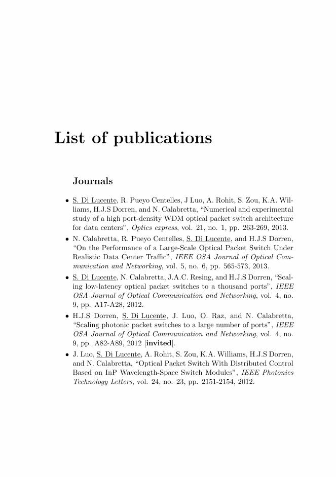
List of publications
Journals
• S. Di Lucente, R. Pueyo Centelles, J Luo, A. Rohit, S. Zou, K.A. Wil-liams, H.J.S Dorren, and N. Calabretta, “Numerical and experimentalstudy of a high port-density WDM optical packet switch architecturefor data centers”, Optics express, vol. 21, no. 1, pp. 263-269, 2013.
• N. Calabretta, R. Pueyo Centelles, S. Di Lucente, and H.J.S Dorren,“On the Performance of a Large-Scale Optical Packet Switch UnderRealistic Data Center Traffic”, IEEE OSA Journal of Optical Com-munication and Networking, vol. 5, no. 6, pp. 565-573, 2013.
• S. Di Lucente, N. Calabretta, J.A.C. Resing, and H.J.S Dorren, “Scal-ing low-latency optical packet switches to a thousand ports”, IEEEOSA Journal of Optical Communication and Networking, vol. 4, no.9, pp. A17-A28, 2012.
• H.J.S Dorren, S. Di Lucente, J. Luo, O. Raz, and N. Calabretta,“Scaling photonic packet switches to a large number of ports”, IEEEOSA Journal of Optical Communication and Networking, vol. 4, no.9, pp. A82-A89, 2012 [invited].
• J. Luo, S. Di Lucente, A. Rohit, S. Zou, K.A. Williams, H.J.S Dorren,and N. Calabretta, “Optical Packet Switch With Distributed ControlBased on InP Wavelength-Space Switch Modules”, IEEE PhotonicsTechnology Letters, vol. 24, no. 23, pp. 2151-2154, 2012.
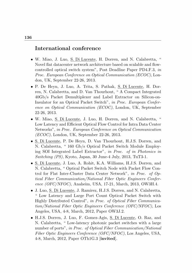
136
International conference
• W. Miao, J. Luo, S. Di Lucente, H. Dorren, and N. Calabretta, “Novel flat datacenter network architecture based on scalable and flow-controlled optical switch system”, Post Deadline Paper PD4.F.3, inProc. European Conference on Optical Communication (ECOC), Lon-don, UK, September 22-26, 2013.
• P. De Heyn, J. Luo, A. Trita, S. Pathak, S. Di Lucente, H. Dor-ren, N. Calabretta, and D. Van Thourhout, “ A Compact Integrated40Gb/s Packet Demultiplexer and Label Extractor on Silicon-on-Insulator for an Optical Packet Switch”, in Proc. European Confer-ence on Optical Communication (ECOC), London, UK, September22-26, 2013.
• W. Miao, S. Di Lucente, J. Luo, H. Dorren, and N. Calabretta, “Low Latency and Efficient Optical Flow Control for Intra Data CenterNetworks”, in Proc. European Conference on Optical Communication(ECOC), London, UK, September 22-26, 2013.
• S. Di Lucente, P. De Heyn, D. Van Thourhout, H.J.S. Dorren, andN. Calabretta, “ 160 Gb/s Optical Packet Switch Module Employ-ing SOI Integrated Label Extractor”, in Proc. of in Photonics inSwitching (PS), Kyoto, Japan, 30 June-4 July, 2013, TuT3-1.
• S. Di Lucente, J. Luo, A. Rohit, K.A. Williams, H.J.S. Dorren, andN. Calabretta, “ Optical Packet Switch Node with Packet Flow Con-trol for Flat Inter-Cluster Data Center Network”, in Proc. of Op-tical Fiber Communication/National Fiber Optic Engineers Confer-ence (OFC/NFOC), Anaheim, USA, 17-21, March, 2013, OW3H.4.
• J. Luo, S. Di Lucente, J. Ramirez, H.J.S. Dorren, and N. Calabretta,“ Low Latency and Large Port Count Optical Packet Switch withHighly Distributed Control”, in Proc. of Optical Fiber Communica-tion/National Fiber Optic Engineers Conference (OFC/NFOC), LosAngeles, USA, 4-8, March, 2012, Paper OW3J.2.
• H.J.S. Dorren, J. Luo, F. Gomez-Agis, S. Di Lucente, O. Raz, andN. Calabretta, “ Low-latency photonic packet switches with a largenumber of ports”, in Proc. of Optical Fiber Communication/NationalFiber Optic Engineers Conference (OFC/NFOC), Los Angeles, USA,4-8, March, 2012, Paper OTh1G.3 [invited].
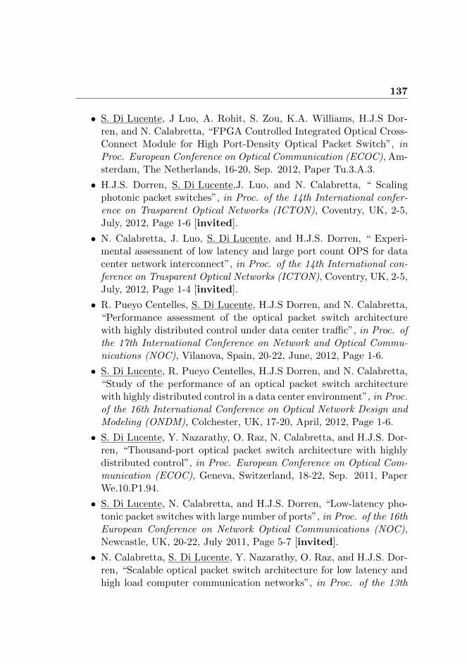
137
• S. Di Lucente, J Luo, A. Rohit, S. Zou, K.A. Williams, H.J.S Dor-ren, and N. Calabretta, “FPGA Controlled Integrated Optical Cross-Connect Module for High Port-Density Optical Packet Switch”, inProc. European Conference on Optical Communication (ECOC), Am-sterdam, The Netherlands, 16-20, Sep. 2012, Paper Tu.3.A.3.
• H.J.S. Dorren, S. Di Lucente,J. Luo, and N. Calabretta, “ Scalingphotonic packet switches”, in Proc. of the 14th International confer-ence on Trasparent Optical Networks (ICTON), Coventry, UK, 2-5,July, 2012, Page 1-6 [invited].
• N. Calabretta, J. Luo, S. Di Lucente, and H.J.S. Dorren, “ Experi-mental assessment of low latency and large port count OPS for datacenter network interconnect”, in Proc. of the 14th International con-ference on Trasparent Optical Networks (ICTON), Coventry, UK, 2-5,July, 2012, Page 1-4 [invited].
• R. Pueyo Centelles, S. Di Lucente, H.J.S Dorren, and N. Calabretta,“Performance assessment of the optical packet switch architecturewith highly distributed control under data center traffic”, in Proc. ofthe 17th International Conference on Network and Optical Commu-nications (NOC), Vilanova, Spain, 20-22, June, 2012, Page 1-6.
• S. Di Lucente, R. Pueyo Centelles, H.J.S Dorren, and N. Calabretta,“Study of the performance of an optical packet switch architecturewith highly distributed control in a data center environment”, in Proc.of the 16th International Conference on Optical Network Design andModeling (ONDM), Colchester, UK, 17-20, April, 2012, Page 1-6.
• S. Di Lucente, Y. Nazarathy, O. Raz, N. Calabretta, and H.J.S. Dor-ren, “Thousand-port optical packet switch architecture with highlydistributed control”, in Proc. European Conference on Optical Com-munication (ECOC), Geneva, Switzerland, 18-22, Sep. 2011, PaperWe.10.P1.94.
• S. Di Lucente, N. Calabretta, and H.J.S. Dorren, “Low-latency pho-tonic packet switches with large number of ports”, in Proc. of the 16thEuropean Conference on Network Optical Communications (NOC),Newcastle, UK, 20-22, July 2011, Page 5-7 [invited].
• N. Calabretta, S. Di Lucente, Y. Nazarathy, O. Raz, and H.J.S. Dor-ren, “Scalable optical packet switch architecture for low latency andhigh load computer communication networks”, in Proc. of the 13th
138
International conference on Trasparent Optical Networks (ICTON),Stockholm, Sweden, 26-30, June, 2011, Page 1-4.
• H.J.S. Dorren, S. Di Lucente,O. Raz, N. Calabretta, and Y. Nazara-thy “ Scaling photonic packet switches to a large number of ports”,in Proc. of International Conference on Information Photonics (IP),Ottawa, Canada, 18-20, May, 2011, Page 1-2.
Symposia
• S. Di Lucente, J Luo, A. Rohit, S. Zou, K.A. Williams, H.J.S Dorren,and N. Calabretta, ”System demonstration of a InP WDM OpticalSwitching Module with FPGA-based Controller as Basic Block forScalable OPS nodes”,in Proc. of the 17th Annual Symposium of theIEEE Photonics Benelux Chapter, Mons, Belgium, Nov. 2012, Page89-92.
• S. Di Lucente, Y. Nazarathy, O. Raz, N. Calabretta, and H.J.S. Dor-ren, ”Controllable thousand-port low-latency optical packet switcharchitecture for short link applications”,in Proc. of the 16th AnnualSymposium of the IEEE Photonics Benelux Chapter, Ghent, Belgium,Dec. 2011, Page 245-248.
• S. Di Lucente, Y. Nazarathy, O. Raz, N. Calabretta, and H.J.S. Dor-ren, ”Fast and scalable optical packet switch architecture for com-puter communication networks”,in Proc. of the 15th Annual Sym-posium of the IEEE Photonics Benelux Chapter, Delft, The Nether-lands, Nov. 2010, Page 73-76.

Acknowledgements
I can finally write the last section of my thesis, late, as usual. It is time tothank all those who have made this thesis possible, directly or indirectly. Ihave met people from all over the world in the last four years and I havelearned from all of them, it has been a great experience.
First of all, I would like to thank my first promotor prof. Harm Dor-ren for giving me the opportunity to work in the ECO group. I want tothank him for his professional supervision, for the patience shown duringhundreds of meetings, for his advices and for guiding me to this importantachievement. I hope I have fulfilled his expectations.
I would like to thank my copromotor dr. Nicola Calabretta. I have beenextremely lucky to work under his guidance. His experience and his energyhave motivated me everyday. I thank him for his support for work-relatedand private matters, I have learned a lot from him.
I would like to thank the committee members for reviewing my thesisand for accepting this role despite their tight schedule. I am particularygrateful to prof. Gabriella Cincotti. This experience is also due to hersuggestions.
I would like to thank Chigo, Fausto, Patty and Julio for the useful dis-cussions and, more important, for their friendship. I am thankful to Aaron,Karen, Prometheus, Nikos, Vlado, Jim, Haoshuo, Pang, Pinxiang, Roy, Cacand Yan. I will miss our international dinners, birthday parties and con-ference trips. I am grateful to Abhinav, Jun and Peter for the great timespent in the lab. Their help during the measurements has been essentialfor the results presented in this thesis. Many thanks to Jose, Brigitta andJolanda for their assistance in the administrative matters and for makingmy work easier. I would like to thank all the other ECO members, it is just

140
impossible to mention one by one by name.
I am thankful to all my basketball teammates and coaches of Tanta-lus and Almonte for the tough practices, games and parties. I thank my“brother from Lebanon” Elie for being always present in the happy and thesad moments, I will always treasure his friendship.
I would like to thank my parents, my brother and my grandmother fortheir constant support and encouragement. I have dedicated this thesis tomy niece Sara and my nephew Marco for the time I could not spend withthem.
It has been a difficult year. It has been even more difficult being closeto me. I am particulary indebted with my girlfriend Gabriella for herinfinite patience. Her unconditional love has supported and inspired mecontinuously.
Stefano Di LucenteEindhoven, December 2013
The Netherlands
Curriculum Vitæ
Stefano Di Lucente was born in Rome, Italy, in July 23rd, 1982. He receivedhis BSc degree in electronic engineering from Roma Tre University in 2006.His BSc thesis was entitled “Development of a wireless device for biomedicaldata and signals acquisition: data transmission module”. He received hisMSc degree cum laude in electronic engineering from Roma Tre Universityin 2009. His MSc thesis was entitled “Scrambling techniques for OCDMAnetworks”.
Since January, 2010, Stefano is a PhD researcher in the Electro-OpticalCommunications group (ECO), department of Electrical Engineering, Eind-hoven University of Technology, under the supervision of Professor H. J. S.Dorren and Dr. N. Calabretta. Stefanos research was conducted under theCommunication Technologies Basic Research and Application (COBRA)research program, funded by the Dutch government.
His research activities are focused on optical packet switching, optical la-beling techniques and optical packet switch control systems. He has workedwith integrated photonic devices, specifically InP optical integrated cross-connect and SOI integrated label extractor based on microring resonators.He has worked with FPGA boards to develop and implement switch controlsystems.
Stefano Di Lucente has published in international conferences and peer-reviewed journals and has acted as supervisor for MSc students. He has re-ceived the best student award OECC/PS for the paper entitled: “160 Gb/sOptical Packet Switch Module Employing SOI Integrated Label Extractor”during the 18th OptoElectronics and Communication Conference/Photonicin Switching Conference in Kyoto, 3rd July 2013.