Embed Size (px)
Citation preview
Accepted Manuscript
Optical properties of silicon-vacancy color centers in diamondcreated by ion implantation and post-annealing
Stefano Lagomarsino, Assegid M. Flatae, Silvio Sciortino,Federico Gorelli, Mario Santoro, Francesco Tantussi, FrancescoDe Angelis, Nicla Gelli, Francesco Taccetti, Lorenzo Giuntini,Mario Agio
PII: S0925-9635(17)30700-8DOI: doi:10.1016/j.diamond.2018.03.010Reference: DIAMAT 7050
To appear in: Diamond & Related Materials
Received date: 7 December 2017Revised date: 8 March 2018Accepted date: 12 March 2018
Please cite this article as: Stefano Lagomarsino, Assegid M. Flatae, Silvio Sciortino,Federico Gorelli, Mario Santoro, Francesco Tantussi, Francesco De Angelis, Nicla Gelli,Francesco Taccetti, Lorenzo Giuntini, Mario Agio , Optical properties of silicon-vacancycolor centers in diamond created by ion implantation and post-annealing. The addressfor the corresponding author was captured as affiliation for all authors. Please check ifappropriate. Diamat(2017), doi:10.1016/j.diamond.2018.03.010
This is a PDF file of an unedited manuscript that has been accepted for publication. Asa service to our customers we are providing this early version of the manuscript. Themanuscript will undergo copyediting, typesetting, and review of the resulting proof beforeit is published in its final form. Please note that during the production process errors maybe discovered which could affect the content, and all legal disclaimers that apply to thejournal pertain.
ACCEP
TED M
ANUSC
RIPT
Optical properties of silicon-vacancy color centers in diamond created by ion implantation
and post-annealing
Authors
Stefano Lagomarsino1,2, Assegid M. Flatae1, Silvio Sciortino2,3, Federico Gorelli4,5, Mario
Santoro4,5, Francesco Tantussi6, Francesco De Angelis6, Nicla Gelli2, Francesco Taccetti2, Lorenzo
Giuntini2,3 and Mario Agio1,4
Affiliations:
1Laboratory of Nano-Optics, University of Siegen, 57072 Siegen, Germany 2Istituto Nazionale di Fisica Nucleare, Sezione di Firenze, 50019 Sesto Fiorentino, Italy 3Department of Physics and Astrophysics, University of Florence, 50019 Sesto Fiorentino, Italy 4National Institute of Optics (INO), National Research Council (CNR), 50019 Sesto Fiorentino,
Italy 5European Laboratory for Nonlinear Spectroscopy (LENS), 50019 Sesto Fiorentino, Italy 6Plasmon Nanotechnologies, Istituto Italiano di Tecnologia, 16163 Genoa, Italy
Keywords: SiV centers, ion implantation, thermal activation, single-photon emitters
Abstract:
Silicon-vacancy (SiV) color centers have been created in diamond by ion implantation and post
annealing at LABEC (Florence). A wide range of implantation depths (0-2.4 m) and fluences
(108-1015 cm-2), along with a variety of substrates (single and poly-crystals) have been explored.
The photoluminescence properties of the SiV centers have been studied at room temperature,
including their single-photon emission characteristics. Single-photon emitters have been obtained
at the lower-end of the implantation fluences range. They exhibit a short excited-state lifetime (1
ns), a strong zero-phonon transition with a narrow linewidth (1.6 nm) and a very small
inhomogeneous broadening (0.015 nm), features that qualify them for application in quantum
optical technologies. The activation yield of SiV centers has been assessed under different
experimental conditions. It has been found to be independent of the implantation energy and in the
range of 3% after thermal annealing.
1 Introduction
Color centers in diamond and other large band-gap semiconductors are promising candidates for
the generation, storage and processing of quantum information1,2,3,4,5, due to the combination of
narrow spectral linewidths, high photon emission rates and optically addressable states with long
coherence times. Compared to the current alternatives, such as trapped ions6, nuclear spins7,
superconductive circuits 8 or semiconductor quantum dots 9 , they have also the advantage of
operating at room (or even higher10) temperature. A significant amount of work has been done in
ACCEPTED MANUSCRIPT
ACCEP
TED M
ANUSC
RIPT
recent years on vacancy_related defects, mainly formed by an interstitial guest splitting two site
vacancies along the 111 direction, like HeV11, SV12, GeV13,14, SnV15 and XeV16 centers. In this
regard, silicon-vacancy (SiV) color centers have recently shown the largest brightness for single-
photon emission at room temperature17 with a fluorescence emission concentrated in the zero-
phonon line (ZPL) at 738 nm18, with a room-temperature linewidth down to 0.7 nm 17. SiV centers
are also investigated in their orbital and electron spin coherence properties, as well as in techniques
for coherent control of their quantum state, in view of possible applications in quantum information
processing19. Moreover, available technologies for the fabrication of photonic waveguides and
microcavities enable miniaturization and scalability of integrated optical devices20,21,22,23.
We have recently developed a facility for the production of color centers in diamond, which is
based on ion implantation in the pristine material followed by thermal activation of the centers in
a high vacuum furnace24. Implantations take place at LABEC, the LABoratory for Environmental
and Cultural heritage of the Florence section of the Italian National Institute of Nuclear Physics
(INFN). The implantation facility is based on a 3MV Tandem accelerator (High Voltage
Engineering Europe) equipped with a HVEE 860 Negative Sputter Ion Source, which allows for
the acceleration of most ion species in the range of energies 1.4-15 MeV, depending on the terminal
voltage and the ion charge state. Properly calibrated metal foils permit, if necessary, to degrade
the ion energy down to a few tens of keV. The facility employs a double electrostatic deflector set-
up for the generation of pulses with a time length selectable from a few ns to some s, and it allows
implantations in a broad range of fluences, from 108 to 1015 cm-2, over areas which vary from a
few m2 to some mm2, depending on the mask employed. Such flexibility is useful to explore a
wide range of implantation depths and fluences. The facility is completed by a custom-designed
furnace for the optical activation of the centers, which allows for the fast heating of irradiated
samples up to 1200 °C in high-vacuum conditions. The annealing procedures are described in
detail in Ref.10, the implantation facility and procedures in Refs.24,25. Here, we report on the optical
properties of SiV color centers obtained in single- and poly-crystalline diamond matrices grown
by chemical vapor deposition (CVD). For the creation of color centers, we accelerate Si3+ ions in
the 6-10 MeV energy range. Since we are interested in the fabrication of emitters placed at depths
varying from a few micrometers up to the shallower layers (within 200 nm from the surface),
which require ion energies down to tens of keV, we have employed energy degraders (2.3 m-
thick Al layers)24. In the following, a detailed description of the setup for the optical
characterization of the SiV centers is presented, along with experiments performed on different
kind of samples obtained by varying the implantation parameters. Implantations at relatively high
fluences (>1011 cm-2) have been performed in single- and poly-crystals, whereas for the
demonstration of single-photon emission, implantations at low fluences (108 – 109 cm-2) in single
crystals have been preferred.
2. Observation of the luminescence of the implanted centers
ACCEPTED MANUSCRIPT
ACCEP
TED M
ANUSC
RIPT
Different techniques have been employed to investigate the optical property of SiV centers created
at different implantation fluences. For high densities (irradiation fluence 1011 cm-2), the SiV
centers have been excited by a 647 nm continuous wave (cw) laser (Ar/Kr ion laser Coherent
Innova 301 Krypton Ion Laser System) and the emission spectrum has been collected using a low
numerical aperture (NA) objective (Mitutoyo Plan Apo SL Infinity-Corrected Objective, 20X, 0.28
NA), with a long working distance (30 mm) in a homebuilt confocal microscope configuration.
The luminescence spectra have been analyzed by means of a single monochromator (Princeton
Acton, Acton sp-500i, 500 mm focal length, 300 lines/mm grating) equipped with a notch filter
(to suppress the laser emission line), and a charge-coupled device (CCD) detector (Princeton
Instruments Spec-10:100BR) cooled below -120 °C by means of a liquid nitrogen reservoir. The
relatively long depth of field of the low-NA objective (about 15 m in air, 2.4 times more in
diamond due to the larger refractive index) has been utilized to compare the luminescence signals
from SiV centers implanted at different depths. The transversal spatial resolution for spectral
detection and imaging of the system is 2 m. The spectral resolution of the spectrometer is 0.3 nm
at the emission wavelength of the SiV center. Micrometric automated XY movement (Newport
translation stages equipped with homemade motorized actuators based on stepping motors
controlled by micro step Pollux boxes) allows the acquisition of the spectra in 2-dimensional
matrices with resolution and repeatability of the order of 1 m.
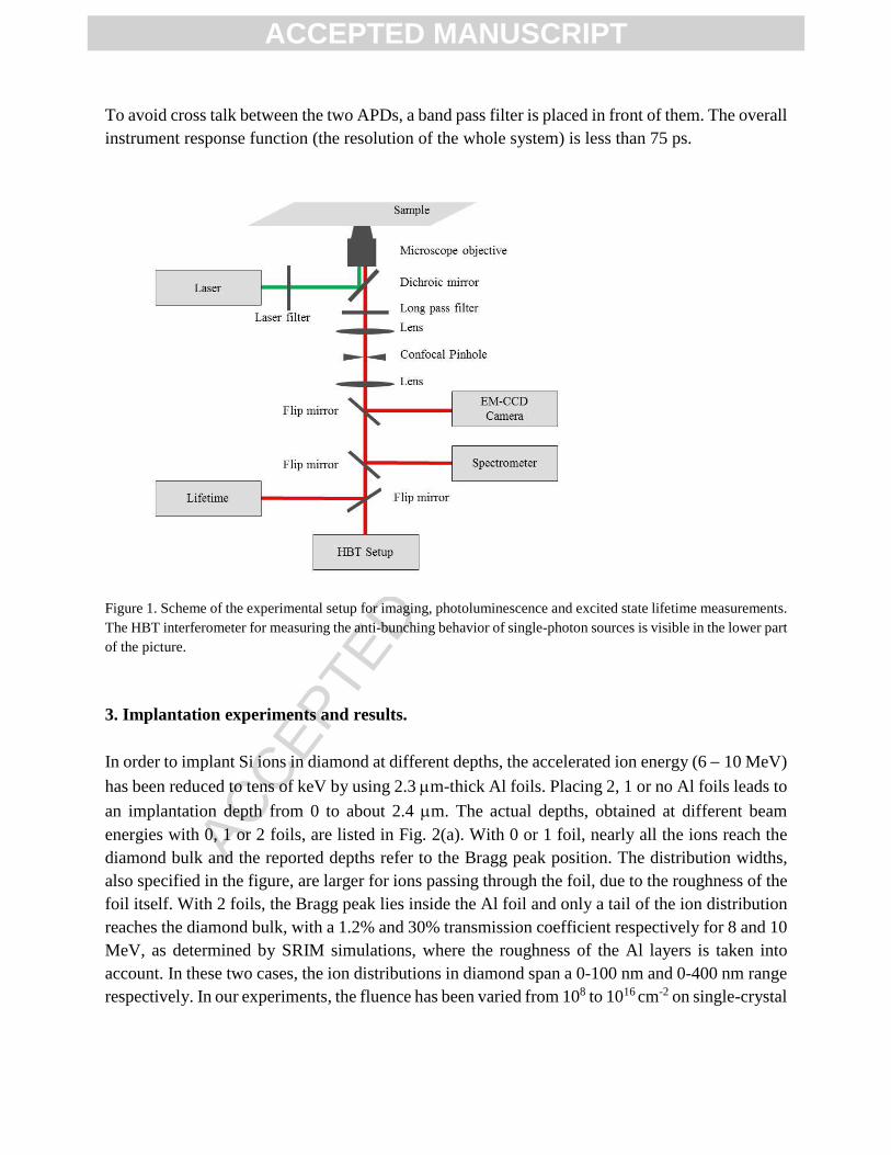
The optical characterization of single SiV centers has been carried out, using another home-made
confocal microscope connected to a spectrometer and a Hanbury-Brown and Twiss (HBT)
interferometer, to measure the second order intensity autocorrelation function, as shown in Fig. 1.
For photoluminescence (PL) measurements the sample is excited by a 647 nm cw laser at a power
< 1mW (Coherent, Innova 70, Ar/Kr ion hybrid) and the emission from the sample is collected via
a cover-slip corrected oil-immersion microscope objective (Olympus, 60X, 1.42 NA, 0.15 mm
working distance). The spectrometer (Horiba, T64000) is equipped with a CCD (Jobin Yvon,
Synapse, front illuminated open electrode, 1024256 pixels) that exhibits a quantum efficiency
around 40–50% at the emission wavelength of the SiV centers. Imaging of single SiV centers is
performed using a flippable reflecting mirror placed along the optical axis of the setup. After wide
field laser illumination, the collected signal is sent to an electron multiplying CCD (EM-CCD)
camera (Princeton Instruments, ProEM-HS: 512 BX3, back-illuminated EMCCD, more than 90%
quantum efficiency at the emission wavelength of the SiV). For measuring the anti-bunching
behavior of SiV centers, a HBT interferometer is used. The laser excites a SiV center and the PL
from the sample is spectrally filtered to suppress the laser line. A 50/50 non-polarizing beam
splitter sends the emitted photons to two avalanche photodiodes (APDs) (Micro Photon Devices,
50 cps dark count). These detectors are connected to the start-stop time-interval analyzer of a time-
correlated single photon counter (TCSPC) (PicoQuant, PicoHarp 300) and the delay between the
arrival times of two emitted photons is repeatedly measured and histogrammed with picosecond
time resolution. The excited-state lifetime of the SiV centers is measured using a pulsed diode
laser (PicoQuant, PDL 800-D, LDH-D-C-660, 656 nm emission wavelength, 45 ps pulse width).
ACCEPTED MANUSCRIPT
ACCEP
TED M
ANUSC
RIPT
To avoid cross talk between the two APDs, a band pass filter is placed in front of them. The overall
instrument response function (the resolution of the whole system) is less than 75 ps.
Figure 1. Scheme of the experimental setup for imaging, photoluminescence and excited state lifetime measurements.
The HBT interferometer for measuring the anti-bunching behavior of single-photon sources is visible in the lower part
of the picture.
3. Implantation experiments and results.
In order to implant Si ions in diamond at different depths, the accelerated ion energy (6 10 MeV)
has been reduced to tens of keV by using 2.3 m-thick Al foils. Placing 2, 1 or no Al foils leads to
an implantation depth from 0 to about 2.4 m. The actual depths, obtained at different beam
energies with 0, 1 or 2 foils, are listed in Fig. 2(a). With 0 or 1 foil, nearly all the ions reach the
diamond bulk and the reported depths refer to the Bragg peak position. The distribution widths,
also specified in the figure, are larger for ions passing through the foil, due to the roughness of the
foil itself. With 2 foils, the Bragg peak lies inside the Al foil and only a tail of the ion distribution
reaches the diamond bulk, with a 1.2% and 30% transmission coefficient respectively for 8 and 10
MeV, as determined by SRIM simulations, where the roughness of the Al layers is taken into
account. In these two cases, the ion distributions in diamond span a 0-100 nm and 0-400 nm range
respectively. In our experiments, the fluence has been varied from 108 to 1016 cm-2 on single-crystal
ACCEPTED MANUSCRIPT
ACCEP
TED M
ANUSC
RIPT
and polycrystalline diamond substrates and the PL has been tested with and without thermal
activation.
In the following we report on three cases because of their relevance in the investigation of the
activation yield of SiV centers and its dependence on several process parameters:
1. Si ions implantation in single crystal diamond at constant fluence (3.2×1013 cm-2), but
different beam energies (6, 8 and 10 MeV) and 0, 1 or 2 Al foils as energy degraders.
Energies and foil thicknesses have been selected in order to obtain approximately equally
spaced end-of-range depths spanning from 0 to 2.4 m. The luminescence spectrum has
been measured before and after annealing at 1100 °C.
2. The same beam energies have been used for Si ion implantation on polycrystalline
diamond, in order to assess possible correlations between the activation yield and the
presence of crystal defects.
3. Implantations at low fluences (108109 cm-2) have been performed in order to observe
single-photon emitters, their spectral characteristics, and directly measure the activation
yield at low fluences.
3.1 High fluence implantations at different depths
A 5×5×0.5 mm3 single-crystal diamond sample by E6®, covered with 0, 1 or 2 Al foils, as shown
in Fig. 2(a), has been irradiated along three horizontal stripes at different energies (6, 8 and 10
MeV) in continuous mode operation. The exit slits of the beamline have been set at 2×0.5 mm2,
and the sample translated horizontally in front of the slits at a constant velocity, forward and
backward, a number of times set in order to obtain an equal ion fluence in each zone. The
irradiation time has been fixed according to the beam current measured before and after
implantation by a Faraday cup, at each energy. As the ion currents is of the order of a few nA,
some tens of cycles are sufficient in each case to obtain a fluence of 3.2×1013 cm-2, with a 30%
systematic error attributed to the Faraday cup measure. Figure 2(a) shows the appearance of the
sample after irradiation but before annealing. Three dark strips ~0.5 mm wide (slightly larger due
to the beam divergence) indicate the damage produced by the Si ions. No darkening is visible in
the areas irradiated through the two foils by 6 and 8 MeV Si ions, because of the full stopping of
the ions in aluminum in the former case and to the very small transmission coefficient (1.2%) in
the latter.
ACCEPTED MANUSCRIPT
ACCEP
TED M
ANUSC
RIPT
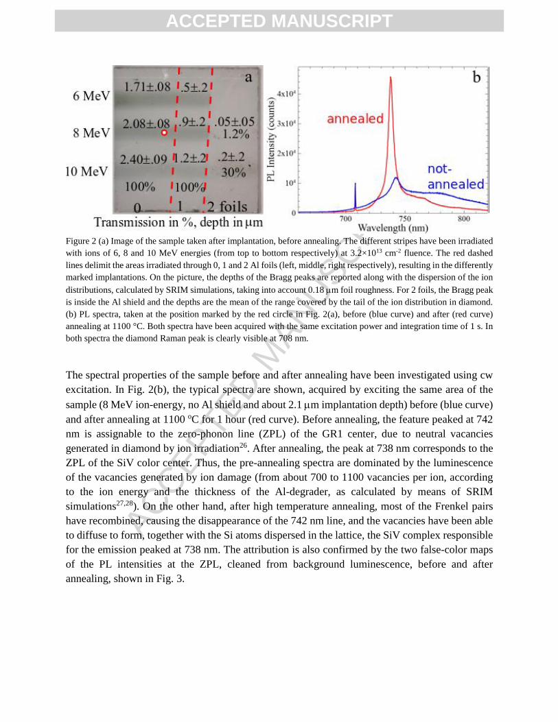
Figure 2 (a) Image of the sample taken after implantation, before annealing. The different stripes have been irradiated
with ions of 6, 8 and 10 MeV energies (from top to bottom respectively) at 3.2×1013 cm-2 fluence. The red dashed
lines delimit the areas irradiated through 0, 1 and 2 Al foils (left, middle, right respectively), resulting in the differently
marked implantations. On the picture, the depths of the Bragg peaks are reported along with the dispersion of the ion
distributions, calculated by SRIM simulations, taking into account 0.18 m foil roughness. For 2 foils, the Bragg peak
is inside the Al shield and the depths are the mean of the range covered by the tail of the ion distribution in diamond.
(b) PL spectra, taken at the position marked by the red circle in Fig. 2(a), before (blue curve) and after (red curve)
annealing at 1100 °C. Both spectra have been acquired with the same excitation power and integration time of 1 s. In
both spectra the diamond Raman peak is clearly visible at 708 nm.
The spectral properties of the sample before and after annealing have been investigated using cw
excitation. In Fig. 2(b), the typical spectra are shown, acquired by exciting the same area of the
sample (8 MeV ion-energy, no Al shield and about 2.1 m implantation depth) before (blue curve)
and after annealing at 1100 oC for 1 hour (red curve). Before annealing, the feature peaked at 742
nm is assignable to the zero-phonon line (ZPL) of the GR1 center, due to neutral vacancies
generated in diamond by ion irradiation26. After annealing, the peak at 738 nm corresponds to the
ZPL of the SiV color center. Thus, the pre-annealing spectra are dominated by the luminescence
of the vacancies generated by ion damage (from about 700 to 1100 vacancies per ion, according
to the ion energy and the thickness of the Al-degrader, as calculated by means of SRIM
simulations27,28). On the other hand, after high temperature annealing, most of the Frenkel pairs
have recombined, causing the disappearance of the 742 nm line, and the vacancies have been able
to diffuse to form, together with the Si atoms dispersed in the lattice, the SiV complex responsible
for the emission peaked at 738 nm. The attribution is also confirmed by the two false-color maps
of the PL intensities at the ZPL, cleaned from background luminescence, before and after
annealing, shown in Fig. 3.
ACCEPTED MANUSCRIPT
ACCEP
TED M
ANUSC
RIPT
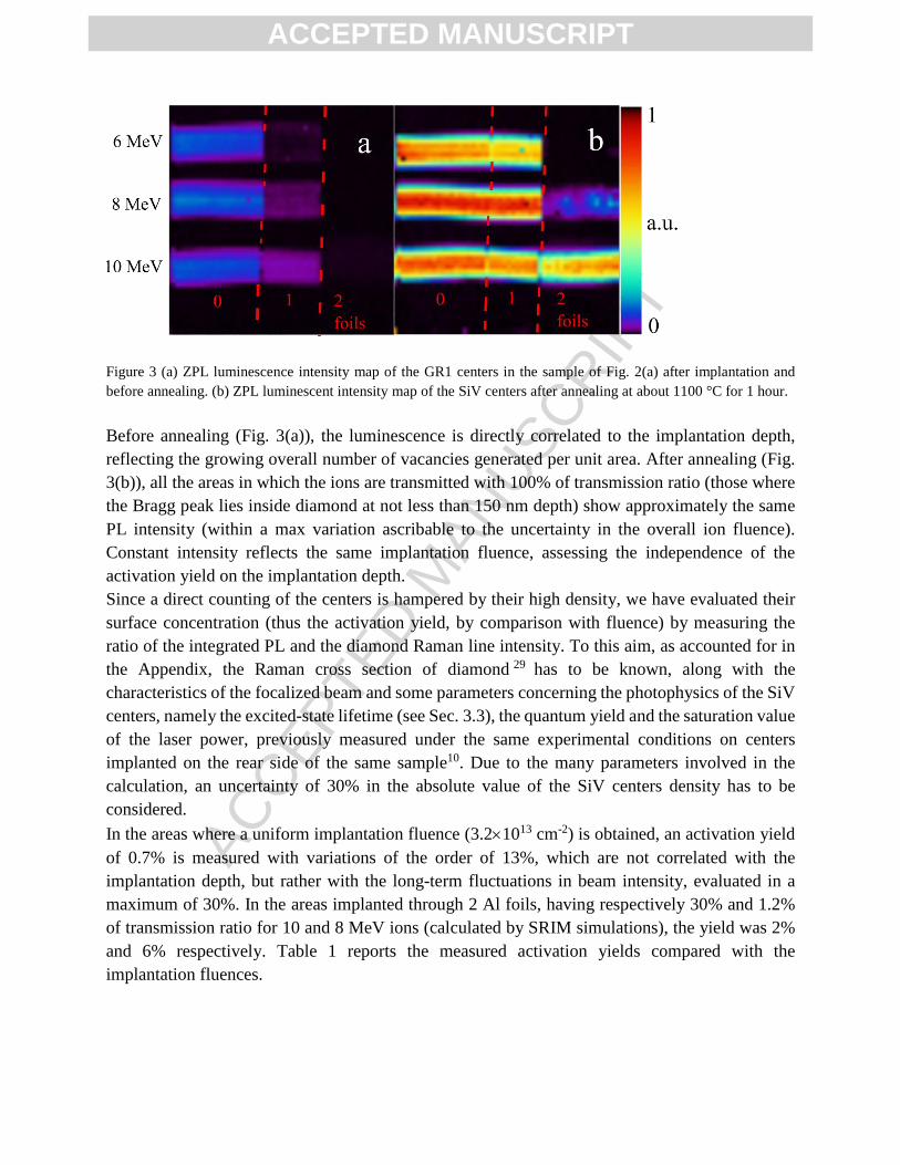
Figure 3 (a) ZPL luminescence intensity map of the GR1 centers in the sample of Fig. 2(a) after implantation and
before annealing. (b) ZPL luminescent intensity map of the SiV centers after annealing at about 1100 °C for 1 hour.
Before annealing (Fig. 3(a)), the luminescence is directly correlated to the implantation depth,
reflecting the growing overall number of vacancies generated per unit area. After annealing (Fig.
3(b)), all the areas in which the ions are transmitted with 100% of transmission ratio (those where
the Bragg peak lies inside diamond at not less than 150 nm depth) show approximately the same
PL intensity (within a max variation ascribable to the uncertainty in the overall ion fluence).
Constant intensity reflects the same implantation fluence, assessing the independence of the
activation yield on the implantation depth.
Since a direct counting of the centers is hampered by their high density, we have evaluated their
surface concentration (thus the activation yield, by comparison with fluence) by measuring the
ratio of the integrated PL and the diamond Raman line intensity. To this aim, as accounted for in
the Appendix, the Raman cross section of diamond 29 has to be known, along with the
characteristics of the focalized beam and some parameters concerning the photophysics of the SiV
centers, namely the excited-state lifetime (see Sec. 3.3), the quantum yield and the saturation value
of the laser power, previously measured under the same experimental conditions on centers
implanted on the rear side of the same sample10. Due to the many parameters involved in the
calculation, an uncertainty of 30% in the absolute value of the SiV centers density has to be
considered.
In the areas where a uniform implantation fluence (3.21013 cm-2) is obtained, an activation yield
of 0.7% is measured with variations of the order of 13%, which are not correlated with the
implantation depth, but rather with the long-term fluctuations in beam intensity, evaluated in a
maximum of 30%. In the areas implanted through 2 Al foils, having respectively 30% and 1.2%
of transmission ratio for 10 and 8 MeV ions (calculated by SRIM simulations), the yield was 2%
and 6% respectively. Table 1 reports the measured activation yields compared with the
implantation fluences.
ACCEPTED MANUSCRIPT
ACCEP
TED M
ANUSC
RIPT
Implantation fluence 3.21013 cm-2 9.61012 cm-2 3.81011 cm-2
Activation yield (30%) 0.7% 2% 6%
Tab 1. Activation yield of the SiV color centers as a function of the implantation fluence for the single-crystal sample.
In principle, the increased activation yield observed for decreasing fluence could depend on the
decreasing implantation depth, but Schröder et al.30, in a study performed at low energies (10-100
keV, thus with 20-70 nm Bragg peak depth) in the 1012 to 1014 cm-2 fluence range, observed a
substiantial independence of the yield on the implantation depth in the first tens of nm, revealing
a remarkable increase with decreasing fluences, down to 1012 cm-2. Our study corroborates these
conclusions extending the implantation depths up to a few microns and confirming a further
increase of the yield down to the 1011 cm-2 fluence range.
The decrease of the yield for increasing fluences could be understood as a consequence of the
presence of inactivated Si bystanders, altering the structure of the defect and possibly inhibiting
the photon emission, e.g. by providing alternative de-excitation channels.
The independence of the activation yield on the implantation depth is not shared by other color
centers, like the nitrogen-vacancy (NV), which show a remarkable decrease of the yield with
decreasing implantation energies31.
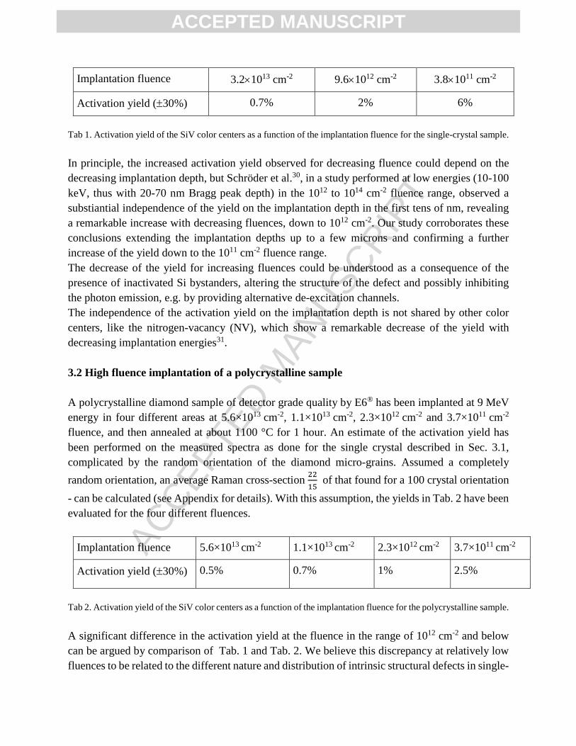
3.2 High fluence implantation of a polycrystalline sample
A polycrystalline diamond sample of detector grade quality by E6® has been implanted at 9 MeV
energy in four different areas at 5.6×1013 cm-2, 1.1×1013 cm-2, 2.3×1012 cm-2 and 3.7×1011 cm-2
fluence, and then annealed at about 1100 °C for 1 hour. An estimate of the activation yield has
been performed on the measured spectra as done for the single crystal described in Sec. 3.1,
complicated by the random orientation of the diamond micro-grains. Assumed a completely
random orientation, an average Raman cross-section 22
15 of that found for a 100 crystal orientation
- can be calculated (see Appendix for details). With this assumption, the yields in Tab. 2 have been
evaluated for the four different fluences.
Implantation fluence 5.6×1013 cm-2 1.1×1013 cm-2 2.3×1012 cm-2 3.7×1011 cm-2
Activation yield (30%) 0.5% 0.7% 1% 2.5%
Tab 2. Activation yield of the SiV color centers as a function of the implantation fluence for the polycrystalline sample.
A significant difference in the activation yield at the fluence in the range of 1012 cm-2 and below
can be argued by comparison of Tab. 1 and Tab. 2. We believe this discrepancy at relatively low
fluences to be related to the different nature and distribution of intrinsic structural defects in single-
ACCEPTED MANUSCRIPT
ACCEP
TED M
ANUSC
RIPT
and poly-crystal diamond, supposedly sites of preferential activation of SiV centers. In single
crystals the prevalent structural defects are dislocations randomly distributed, in poly-crystals
grain boundaries present a characteristic distribution, whose cross section on the surface is roughly
polygonal.
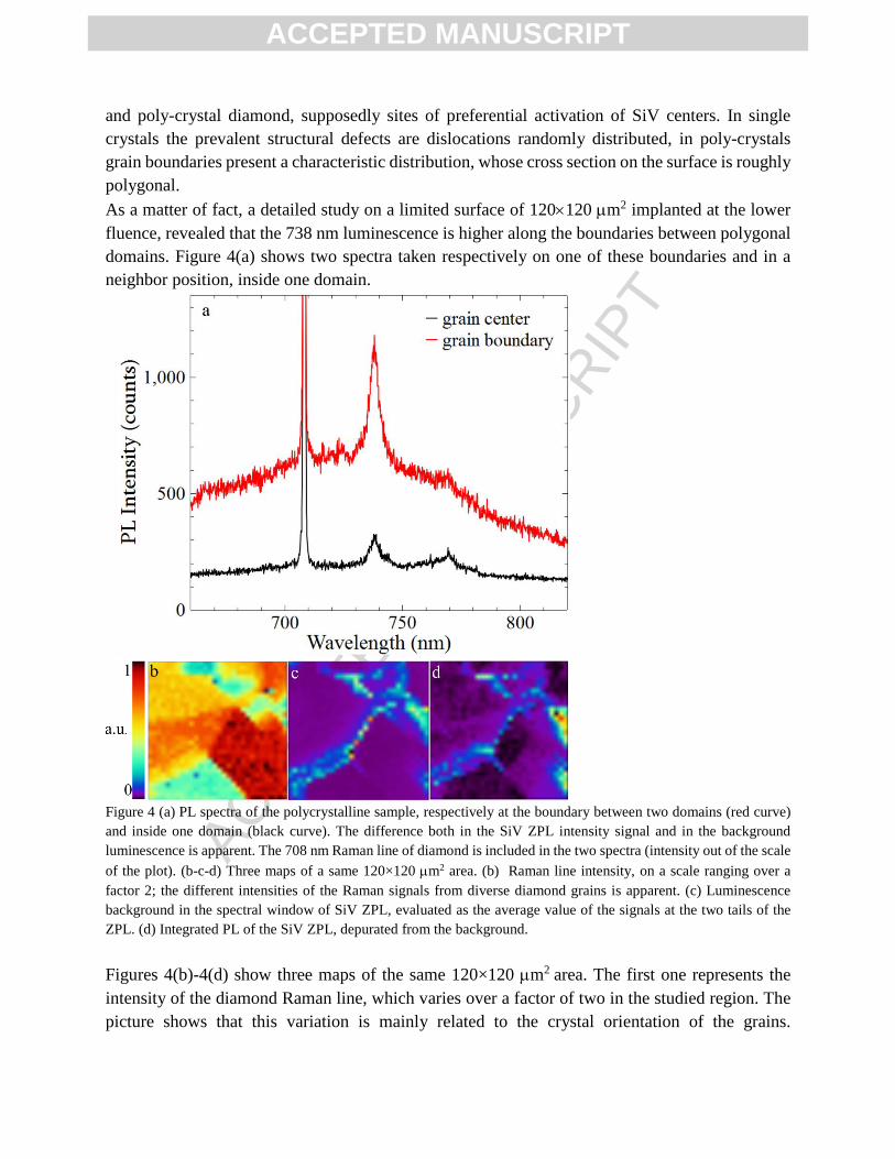
As a matter of fact, a detailed study on a limited surface of 120120 m2 implanted at the lower
fluence, revealed that the 738 nm luminescence is higher along the boundaries between polygonal
domains. Figure 4(a) shows two spectra taken respectively on one of these boundaries and in a
neighbor position, inside one domain.
Figure 4 (a) PL spectra of the polycrystalline sample, respectively at the boundary between two domains (red curve)
and inside one domain (black curve). The difference both in the SiV ZPL intensity signal and in the background
luminescence is apparent. The 708 nm Raman line of diamond is included in the two spectra (intensity out of the scale
of the plot). (b-c-d) Three maps of a same 120×120 m2 area. (b) Raman line intensity, on a scale ranging over a
factor 2; the different intensities of the Raman signals from diverse diamond grains is apparent. (c) Luminescence
background in the spectral window of SiV ZPL, evaluated as the average value of the signals at the two tails of the
ZPL. (d) Integrated PL of the SiV ZPL, depurated from the background.
Figures 4(b)-4(d) show three maps of the same 120×120 m2 area. The first one represents the
intensity of the diamond Raman line, which varies over a factor of two in the studied region. The
picture shows that this variation is mainly related to the crystal orientation of the grains.
ACCEPTED MANUSCRIPT
ACCEP
TED M
ANUSC
RIPT
Furthermore, it is apparent that the Raman line intensity varies from grain to grain, whose size is
in the range from tens to a hundred of microns. The second map shows the background
luminescence, arguably related to defects, which appear to be distributed along grain boundaries,
as expected. The third map shows the spatial distribution of the SiV ZPL intensity, isolated from
the background contribution (which has been obtained by subtracting a value corresponding to the
average of the two tails). The close correlation between the density of the activated SiV centers
and the grain boundaries is evident. The ratio 4:1 between the activation yield along the grain
boundary and that in the grain center suggested by the two spectra of Fig. 4 (a) seems to be quite
typical. The analysis shows that the activation of the SiV centers is much more probable where the
native defects concentration is higher. This is reasonable as long as the center activation depends
on the formation of complexes composed by a Si atom and a vacancy32.
3.3 Low fluence implantation for single-photon sources
To demonstrate the potential of the technique for the fabrication of SiV-based single-photon
sources, a CVD single-crystal diamond sample has been chosen. The ions have been implanted
with fluences in the range of 108 - 109 cm-2 at depths ranging from a few tens of nm (8-9 MeV
energies with 2 Al shields) to about 2 μm (10 MeV without shields). The samples have been
annealed at 1000-1150 °C for 1 hour.
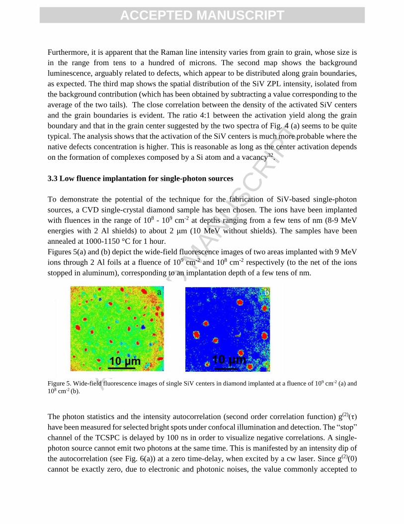
Figures 5(a) and (b) depict the wide-field fluorescence images of two areas implanted with 9 MeV
ions through 2 Al foils at a fluence of 109 cm-2 and 108 cm-2 respectively (to the net of the ions
stopped in aluminum), corresponding to an implantation depth of a few tens of nm.
Figure 5. Wide-field fluorescence images of single SiV centers in diamond implanted at a fluence of 109 cm-2 (a) and
108 cm-2 (b).
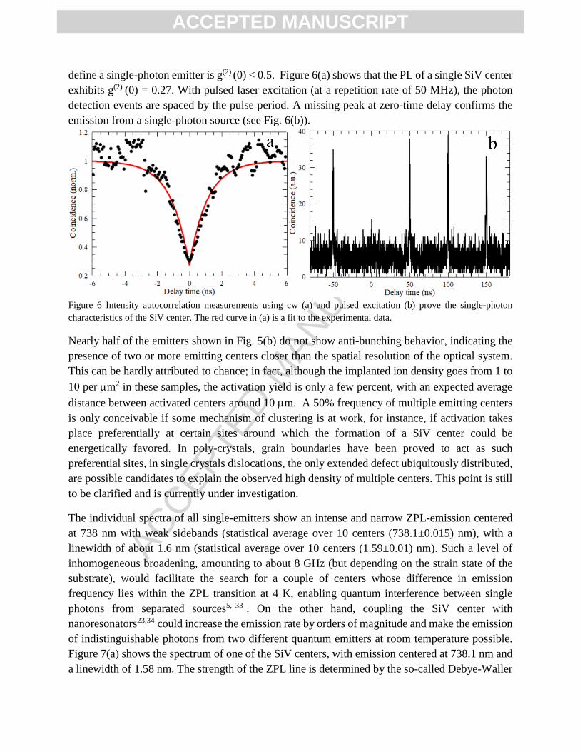
The photon statistics and the intensity autocorrelation (second order correlation function) g(2)(τ)
have been measured for selected bright spots under confocal illumination and detection. The “stop”
channel of the TCSPC is delayed by 100 ns in order to visualize negative correlations. A single-
photon source cannot emit two photons at the same time. This is manifested by an intensity dip of
the autocorrelation (see Fig. 6(a)) at a zero time-delay, when excited by a cw laser. Since g(2)(0)
cannot be exactly zero, due to electronic and photonic noises, the value commonly accepted to
ACCEPTED MANUSCRIPT
ACCEP
TED M
ANUSC
RIPT
define a single-photon emitter is g(2) (0) < 0.5. Figure 6(a) shows that the PL of a single SiV center
exhibits g(2) (0) = 0.27. With pulsed laser excitation (at a repetition rate of 50 MHz), the photon
detection events are spaced by the pulse period. A missing peak at zero-time delay confirms the
emission from a single-photon source (see Fig. 6(b)).
Figure 6 Intensity autocorrelation measurements using cw (a) and pulsed excitation (b) prove the single-photon
characteristics of the SiV center. The red curve in (a) is a fit to the experimental data.
Nearly half of the emitters shown in Fig. 5(b) do not show anti-bunching behavior, indicating the
presence of two or more emitting centers closer than the spatial resolution of the optical system.
This can be hardly attributed to chance; in fact, although the implanted ion density goes from 1 to
10 per m2 in these samples, the activation yield is only a few percent, with an expected average
distance between activated centers around 10 m. A 50% frequency of multiple emitting centers
is only conceivable if some mechanism of clustering is at work, for instance, if activation takes
place preferentially at certain sites around which the formation of a SiV center could be
energetically favored. In poly-crystals, grain boundaries have been proved to act as such
preferential sites, in single crystals dislocations, the only extended defect ubiquitously distributed,
are possible candidates to explain the observed high density of multiple centers. This point is still
to be clarified and is currently under investigation.
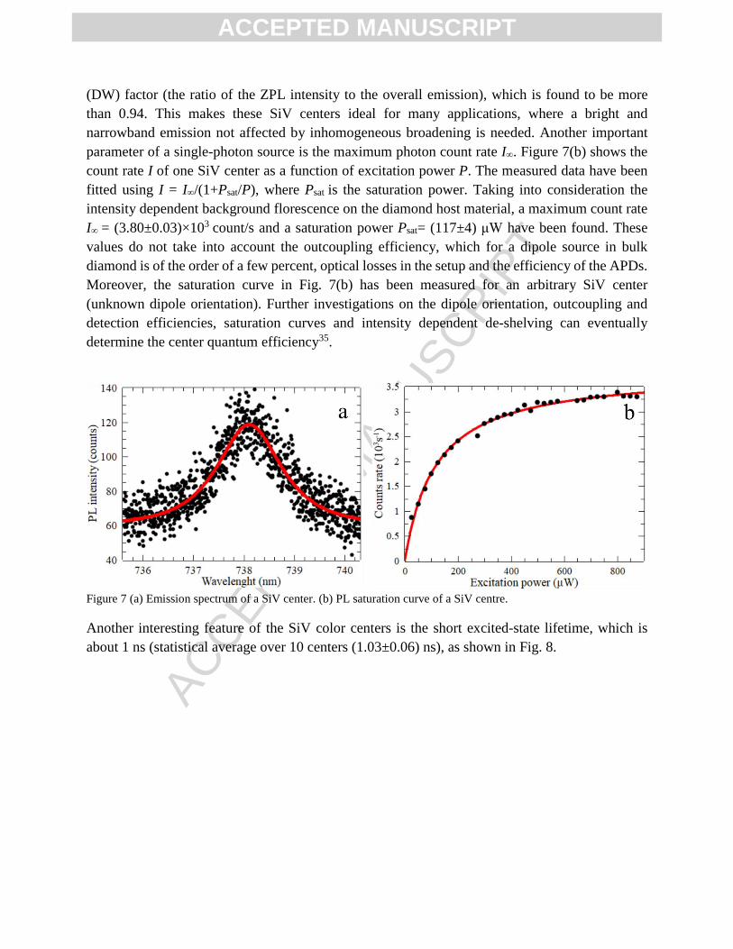
The individual spectra of all single-emitters show an intense and narrow ZPL-emission centered
at 738 nm with weak sidebands (statistical average over 10 centers (738.1±0.015) nm), with a
linewidth of about 1.6 nm (statistical average over 10 centers (1.59±0.01) nm). Such a level of
inhomogeneous broadening, amounting to about 8 GHz (but depending on the strain state of the
substrate), would facilitate the search for a couple of centers whose difference in emission
frequency lies within the ZPL transition at 4 K, enabling quantum interference between single
photons from separated sources5, 33 . On the other hand, coupling the SiV center with
nanoresonators23,34 could increase the emission rate by orders of magnitude and make the emission
of indistinguishable photons from two different quantum emitters at room temperature possible.
Figure 7(a) shows the spectrum of one of the SiV centers, with emission centered at 738.1 nm and
a linewidth of 1.58 nm. The strength of the ZPL line is determined by the so-called Debye-Waller
ACCEPTED MANUSCRIPT
ACCEP
TED M
ANUSC
RIPT
(DW) factor (the ratio of the ZPL intensity to the overall emission), which is found to be more
than 0.94. This makes these SiV centers ideal for many applications, where a bright and
narrowband emission not affected by inhomogeneous broadening is needed. Another important
parameter of a single-photon source is the maximum photon count rate I∞. Figure 7(b) shows the
count rate I of one SiV center as a function of excitation power P. The measured data have been
fitted using I = I∞/(1+Psat/P), where Psat is the saturation power. Taking into consideration the
intensity dependent background florescence on the diamond host material, a maximum count rate
I∞ = (3.80±0.03)×103 count/s and a saturation power Psat= (117±4) μW have been found. These
values do not take into account the outcoupling efficiency, which for a dipole source in bulk
diamond is of the order of a few percent, optical losses in the setup and the efficiency of the APDs.
Moreover, the saturation curve in Fig. 7(b) has been measured for an arbitrary SiV center
(unknown dipole orientation). Further investigations on the dipole orientation, outcoupling and
detection efficiencies, saturation curves and intensity dependent de-shelving can eventually
determine the center quantum efficiency35.
Figure 7 (a) Emission spectrum of a SiV center. (b) PL saturation curve of a SiV centre.
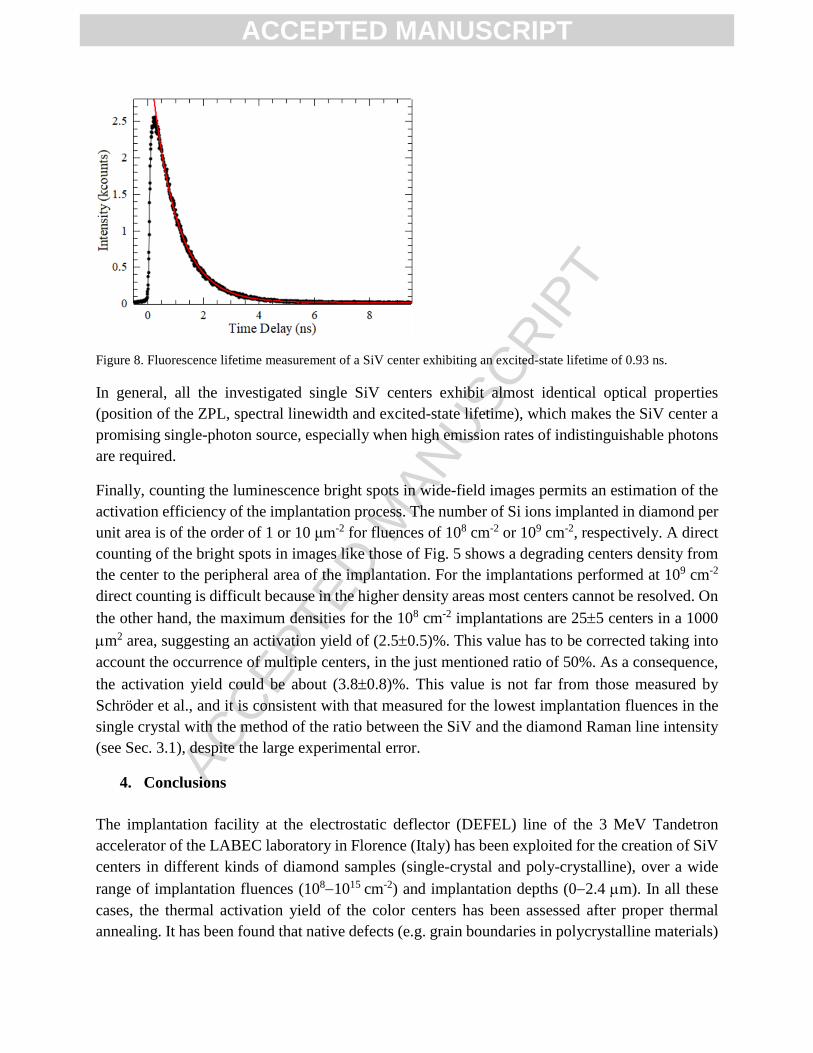
Another interesting feature of the SiV color centers is the short excited-state lifetime, which is
about 1 ns (statistical average over 10 centers (1.03±0.06) ns), as shown in Fig. 8.
ACCEPTED MANUSCRIPT
ACCEP
TED M
ANUSC
RIPT
Figure 8. Fluorescence lifetime measurement of a SiV center exhibiting an excited-state lifetime of 0.93 ns.
In general, all the investigated single SiV centers exhibit almost identical optical properties
(position of the ZPL, spectral linewidth and excited-state lifetime), which makes the SiV center a
promising single-photon source, especially when high emission rates of indistinguishable photons
are required.
Finally, counting the luminescence bright spots in wide-field images permits an estimation of the
activation efficiency of the implantation process. The number of Si ions implanted in diamond per
unit area is of the order of 1 or 10 μm-2 for fluences of 108 cm-2 or 109 cm-2, respectively. A direct
counting of the bright spots in images like those of Fig. 5 shows a degrading centers density from
the center to the peripheral area of the implantation. For the implantations performed at 109 cm-2
direct counting is difficult because in the higher density areas most centers cannot be resolved. On
the other hand, the maximum densities for the 108 cm-2 implantations are 255 centers in a 1000
m2 area, suggesting an activation yield of (2.50.5)%. This value has to be corrected taking into
account the occurrence of multiple centers, in the just mentioned ratio of 50%. As a consequence,
the activation yield could be about (3.80.8)%. This value is not far from those measured by
Schröder et al., and it is consistent with that measured for the lowest implantation fluences in the
single crystal with the method of the ratio between the SiV and the diamond Raman line intensity
(see Sec. 3.1), despite the large experimental error.
4. Conclusions
The implantation facility at the electrostatic deflector (DEFEL) line of the 3 MeV Tandetron
accelerator of the LABEC laboratory in Florence (Italy) has been exploited for the creation of SiV
centers in different kinds of diamond samples (single-crystal and poly-crystalline), over a wide
range of implantation fluences (1081015 cm-2) and implantation depths (02.4 m). In all these
cases, the thermal activation yield of the color centers has been assessed after proper thermal
annealing. It has been found that native defects (e.g. grain boundaries in polycrystalline materials)
ACCEPTED MANUSCRIPT
ACCEP
TED M
ANUSC
RIPT
enhance the thermal activation of SiV centers, while the implantation depth is quite irrelevant,
differently from other implanted color centers like NV31. In the low fluence regime, the activation
yield also seems to be independent on the implantation fluence.
The single-photon emission characteristics of the SiV centers have been verified using PL and
time-resolved spectroscopy. Most of the fluorescence signal is concentrated in the narrow ZPL at
738 nm, with a room temperature linewidth down to 1.6 nm. This is due to a very large Debye-
Waller factor, which reaches 0.94. Moreover, the SiV centers exhibit a very small inhomogeneous
broadening ( 0.015 nm around the ZPL) and a short excited-state lifetime ( 1 ns). These features
make the SiV centers ideal candidates for many applications based on single-photon emitters. In
particular, the spectral quality and reproducibility of the optical properties make these solid-state
emitters promising for the production of indistinguishable photons from separated centers.
Prime novelty statement
We have assessed the correlation between the activation yield of implanted SiV centers and the
native defects concentration in polycrystalline diamond. We have applied an innovative method
for the measurement of the activation yield for high density implantations based on comparison
between the SiV and the diamond Raman line intensity. We have found that, differently from other
implanted color centers, the activation yield of the SiV is independent on the implantation energy.
We found that SiV centers implanted at LABEC exhibit spectral quality and reproducibility
suitable for quantum applications, for instance for the scalable production of bright single photon
sources.
Acknowledgments
Financial support from the EC Seventh Framework Programme (248855), the Helmoltz
Association (283286), the University of Siegen and Istituto Italiano di Tecnologia is gratefully
acknowledged. The authors warmly thank INFN-CHNet, the network of laboratories of the INFN
for cultural heritage, for support and precious contributions in terms of instrumentation and
personnel. This article is based upon work from COST Action MP1403 “Nanoscale Quantum
Optics,” supported by COST (European Cooperation in Science and Technology). We gratefully
thank also Nicole Fabbri, Costanza Toninelli and Silvia Orlanducci for helpful discussions.
Appendix: Evaluation of the SiV surface density by comparison of the SiV luminescence and
the Raman line intensity
The number of SiV centers activated per unit area nSiV can be evaluated measuring the ratio between
their integrated luminosity and that of the diamond Raman line. This can be assumed to be comparable to
the ratio between the number of photons 𝑑𝑁𝑆𝑖𝑉
𝑑𝑡 , emitted in the backward direction per unit solid angle by
the SiV centers in the unit time, and 𝑑𝑁𝑅
𝑑𝑡, the number of those backscattered by diamond due to Raman
ACCEPTED MANUSCRIPT
ACCEP
TED M
ANUSC
RIPT
effect. Both these photon fluxes comes from the same volume V, equaling the cross section of the laser
beam waist S times nd/2, the product of half the depth of field d and the refraction index n of diamond
(n=2.41). The two ratios are assumed equal providing that the transfer function of the optical system is
weakly dependent on the wavelength and that the collection efficiencies for the fluorescence and Raman
signals are the same.
Now
𝑑𝑁𝑅
𝑑𝑡=
�̅�
ℎ𝑃𝑙𝑎𝑛𝑘𝜈𝐿∙ 𝑆 ∙
𝑛𝑑
2∙ 𝑛𝐶 ∙ 𝜎𝑅.
Where R is the Raman differential cross section in the backward direction, nC is the density of carbon
atoms (1.76×1023 cm-3), vL is the frequency of the laser photons (647 nm in our case) and �̅�=P/S is the
average illuminance in the volume V, given by the ratio between the laser power transmitted in diamond
and the laser beam cross section S (used values are reported below).
Thus, we have
𝑑𝑁𝑆𝑖𝑉
𝑑𝑡= 𝜚 ∙
𝑃
ℎ𝑃𝑙𝑎𝑛𝑘𝜈𝐿∙
𝑛𝑑
2∙ 𝑛𝐶 ∙ 𝜎𝑅.
Now, if the emission of the centers is assumed isotropic, due to their random orientation in the diamond
lattice, 𝑑𝑁𝑆𝑖𝑉
𝑑𝑡 is bound to the density of the excited SiV centers 𝑛𝑆𝑖𝑉
∗ by the equation
𝑑𝑁𝑆𝑖𝑉
𝑑𝑡=
1
4𝜋
𝜂
𝜏𝑛𝑆𝑖𝑉
∗ ∙ 𝑆,
Where is the quantum yield and is the lifetime of the excited level. On the other hand, nSiV* depends
on the power level P according to
𝑛𝑆𝑖𝑉∗ =
𝑃
𝑃 + 𝑃𝑠𝑎𝑡𝑛𝑆𝑖𝑉
So that we find
𝑛𝑆𝑖𝑉 = 𝜚 ∙𝜏
𝜂∙
(𝑃 + 𝑃𝑠𝑎𝑡)/𝑆
ℎ𝜈𝐿∙
𝑛𝑑
2∙ 𝑛𝐶 ∙ 4𝜋𝜎𝑅.
In our measurements, we have =1.1 ns, P36 mW, Psat=75 mW, S=10-8cm2, d=20m. is evaluated as
30% for SiV centers in diamond bulk. The quantity 4R has been measured in backscattering
configuration for a 111 oriented crystal and equals, at i= 785 nm of excitation wavelength (s= 877 nm
scattered wavelength), 2.710-29 cm2 per carbon atom29. Our crystals are 100 oriented, so the Raman cross
section reduces to 3/5 of the value relative to the 111 direction of propagation.
ACCEPTED MANUSCRIPT
ACCEP
TED M
ANUSC
RIPT
The ratio of the two Raman cross sections for unpolarized scattered light has been calculated taking into
account 𝜎𝑅 = ∑ (𝑒𝐼𝛼𝑖𝑖𝑗 𝑒𝑗𝑅)2 where i is the Raman polarizability tensor relative to the i-th irreducible
representation of the punctual group of the crystal, eI is the polarization vector of the incident light and eRj
are the two orthogonal polarization vectors of the scattered light. For diamond the non-null tensors
referred to the 100, 010 and 001 directions are36 (0 0 00 0 𝑑0 𝑑 0
) ; (0 0 𝑑0 0 0𝑑 0 0
) ; (0 𝑑 0𝑑 0 00 0 0
)
The excitation wavelength is ’i= 647 nm (’s =708 nm scattered light), so the Raman cross section per
carbon atom in our experimental conditions can be evaluated as
4𝜋𝜎𝑅(100)
(𝜆𝑖′) =
3
5∙
𝜆𝑠3𝜆𝑖
𝜆𝑠′3𝜆𝑖′4𝜋𝜎𝑅
(111)(𝜆𝑖) = 3.7 ∙ 10−29𝑐𝑚2
Once nSiV has been evaluated, the activation yield is promptly calculated as /nSiV, where is the
implantation fluence.
In the case of the polycrystalline sample, the Raman cross section R(,) for a random orientation of the
crystal has been calculated and the ratio ∫ 𝜎𝑅(𝜃, 𝜑)𝑐𝑜𝑠𝜃𝑑𝜃𝑑𝜑/ 𝜎𝑅(< 100 >) =22
15 has been taken into
account.
ACCEPTED MANUSCRIPT
ACCEP
TED M
ANUSC
RIPT
1 C. Kurtsiefer, S. Mayer, P. Zarda & H. Weinfurter Stable solid-state source of single photons. Phys. Rev. Lett. 85,
290–293 (2000) 2 B.J.M. Hausmann, B. Shields, Q. Quan, P. Maletinsky, M. McCutcheon, J.T. Choy, T.M. Babinec, A. Kubanek, A.
Yacoby, M.D. Lukin and M. Loncar, Integrated Diamond Networks for Quantum Nanophotonics. Nano Lett. 12,
1578 (2012) 3 F. Fuchs, B. Stender, M. Trupke, D. Simin, J. Pflaum, V. Dyakonov & G.V. Astakhov. Engineering near-infrared
single-photon emitters with optically active spins in ultrapure silicon carbide. Nat. Commun. 6, Article number:
7578 (2015) 4 M. Widmann, S.Y. Lee, T. Rendler, N. Tien Son, H. Fedder, S. Paik, Li-Ping Yang, N. Zhao, S. Yang, I. Booker,
A. Denisenko, M. Jamali, S.A. Momenzadeh, I. Gerhardt, T. Ohshima, A. Gali, E. Janzén and J. Wrachtrup.
Coherent control of single spins in silicon carbide at room temperature. Nat. Mater. 14, 164–168 (2015). 5 A. Sipahigil, K. D. Jahnke, L. J. Rogers, T. Teraji, J. Isoya, A. S. Zibrov, F. Jelezko and M. D. Lukin.
Indistinguishable Photons from Separated Silicon-Vacancy Centers in Diamond. PRL 113, 113602 (2014) 6 R. Blatt and D. Wineland. Entangled states of trapped atomic ions. Nature 453, 1008–15 (2008)
7 L.M. Vandersypen, M. Steffen, G. Breyta, C.S. Yannoni, M.H. Sherwood and I.L. Chuang. Experimental
realization of Shor’s quantum factoring algorithm using nuclear magnetic resonance. Nature 414, 883–7 (2001) 8 C. Rigetti, J.M. Gambetta, S. Poletto, B.L.T. Plourde, J.M. Chow, D. Córcoles, J.A. Smolin, S.T. Merkel, J.R.
Rozen, G.A. Keefe, M.B. Rothwell, M.B. Ketchen and M. Steffen. Superconducting qubit in a waveguide cavity
with a coherence time approaching 0.1 ms. Phys. Rev. B 86, 100506 (2012) 9 D. Press, T.D. Ladd, B. Zhang and Y. Yamamoto. Complete quantum control of a single quantum dot spin using
ultrafast optical pulses. Nature 456, 218–21 (2008). 10 S. Lagomarsino, F. Gorelli, M. Santoro, N. Fabbri, A. Hajeb, S. Sciortino, L. Palla, C. Czelusniak, M. Massi, F.
Taccetti, L. Giuntini, N. Gelli, D. Y. Fedyanin, F.S. Cataliotti, C. Toninelli and M. Agio. Robust luminescence of the
silicon-vacancy center in diamond at high temperatures. AIP ADVANCES 5, 127117 (2015) 11 J. Forneris, A. Tengattini, S. Ditalia Tchernij, F. Picollo, A. Battiato, P. Traina, P. Degiovanni, E. Moreva, G.
Brida, V. Grilj, N. Skukan, M. Jakšić, M. Genovese, P. Olivero, Creation and characterization of He-related color
centers in diamond, Journal of Luminescence, 179 (2016) 59-63 12 G.D. Cheng, Q. Huang, Y.H. Shen, H.F. Huang, L. Yan, Theory of sulfur-vacancy defect in diamond: a
comparable NV−1 isoelectronic center, Electron Optics 136 (2017) 151-156 13
M. K. Bhaskar, D. D. Sukachev, A. Sipahigil, R. E. Evans, M. J. Burek, C. T. Nguyen, L. J. Rogers, P. Siyushev,
M. H. Metsch, H. Park, F. Jelezko, M. Lončar, and M. D. Lukin. Quantum Nonlinear Optics with a Germanium-
Vacancy Color Center in a Nanoscale Diamond Waveguide. Phys. Rev. Lett. 118, 223603 – Published 31 May 2017 14 K.N. Boldyrev, B.N. Mavrin, P.S. Sherin, M.N.Popova, Bright luminescence of diamonds with Ge-V centers,
Journal of Luminescence 193 (2018) 119-124 15
T. Iwasaki, Y. Miyamoto, T. Taniguchi, P. Siyushev, M.H. Metsch, F. Jelezko and M. Hatano Tin-Vacancy
Quantum Emitters in Diamond. Phys. Rev. Lett. 119, 253601 – Published 22 December 2017 16
R. Sandstrom, L. Ke, A. Martin, Z.Wang, M. Kianinia, B. Green, W.-b. Gao, I. Aharonovich, Optical properties
of implanted Xe color centers in diamond, Optics Communications 411 (2018) 182-186 17 E. Neu, D. Steinmetz, J. Riedrich-Mӧller, S. Gsell, M. Fischer, M. Schreck, and C. Becher. Single photon
emission from silicon-vacancy colour centres in chemical vapour deposition nano-diamonds on iridium. New J.
Phys. 13, 025012 (2011) 18 S. Pezzagna, D. Rogalla, D. Wildanger, J. Meijer and A. Zaitsev. Creation and nature of optical centres in
diamond for single-photon emission—overview and critical remarks. New Journal of Physics 13(2011) 035024
ACCEPTED MANUSCRIPT
ACCEP
TED M
ANUSC
RIPT
19 J.N. Becker, C. Becker. Coherence Properties and Quantum Control of Silicon Vacancy Color Centers in
Diamond. Phys. Status Solidi A, 1700586 (2017) 20 M.P. Hiscocks, K. Ganesan, B.C. Gibson, S.T. Huntington, F. Ladouceur and S. Prawer. Diamond waveguides
fabricated by reactive ion etching. Optics Express, 16:19512, 2010. 21 S. Lagomarsino, P. Olivero, F. Bosia, M. Vannoni, S. Calusi, L. Giuntini, M. Massi. Evidence of light guiding in
ion-implanted diamond. Physical review letters. 105, (2010) 233903 22 T.M. Babinec, B.J.M. Hausmann, M. Khan, Y. Zhang, J.R. Maze, P.R. Hemmer & M. Lončar. A diamond
nanowire single-photon source. Nature Nanotechnology 5, 195 - 199 (2010) 23 J. Riedrich-Möller, L. Kipfstuhl, C. Hepp, E. Neu, C. Pauly, F. Mücklich, A. Baur, M. Wandt, S. Wolff, M.
Fischer, S. Gsell, M. Schreck & C. Becher. One- and two-dimensional photonic crystal microcavities in single
crystal diamond. Nature Nanotechnology 7, 69–74 (2012) 24
S. Lagomarsino, S. Sciortino, N. Gelli, A. M. Flatae, F. Gorelli, M. Santoro, M. Chiari, C. Czelusniak, M. Massi,
F. Taccetti, M. Agio, and L. Giuntini. The center for production of single-photon emitters at the electrostatic-
deflector line of the Tandem Accelerator of LABEC (Florence) Nuclear Instruments and Methods in Physics
Research B 422 (2018) 31-40 25 N. Taccetti, L. Giuntini, G. Casini, A.A. Stefanini, M. Chiari, M.E. Fedi, P.A. Mandò, The pulsed beam facility
at the 3 MV Van de Graaff accelerator in Florence: Overview and examples of applications, Nuclear Instruments
and Methods in Physics Research B 188 (2002) 255-260 26
I. Kiflawi, A.T. Collins, K. Iakoubovskii and D. Fisher. Electron irradiation and the formation of
vacancy–interstitial pairs in diamond. J. Phys.: Condens. Matter 19 (2007) 046216 27
J.F. Ziegler, M.D. Ziegler, J.P. Biersack, SRIM – The stopping and range of ions in matter (2010), Nuclear
Instruments and Methods in Physics Research B 268 (2010) 1818–1823 28
http://www.srim.org 29 R.L. Aggarwal, L.W. Farrar, S.K. Saikin , X. Andrade, A. Aspuru-Guzik, D.L. Polla. Measurement of the
absolute Raman cross section of the optical phonons in type Ia natural diamond. Solid State Communications 152
(2012) 204–209 30 T. Schröder, M. E. Trusheim, M. Walsh, L. Li, J. Zheng, M. Schukraft, A. Sipahigil, R. E. Evans, D.D. Sukachev,
C.T. Nguyen, J.L. Pacheco, R.M. Camacho, E.S. Bielejec, M.D. Lukin & D. Englund. Scalable focused ion beam
creation of nearly lifetime-limited single quantum emitters in diamond nanostructures. Nature Communications 8,
(2017) 15376. 31
S. Pezzagna, B. Naydenov, F. Jelezko, J. Wrachtrup and J. Meijer. Creation efficiency of nitrogen-vacancy
centres in diamond. New Journal of Physics 12, 065017 (2010) 32 U. F. S. D'Haenens-Johansson, A. M. Edmonds, B. L. Green, M. E. Newton, G. Davies, P. M. Martineau, R. U. A.
Khan, and D. J. Twitchen. Optical properties of the neutral silicon split-vacancy center in diamond. Phys. Rev. B 84
(2011) 245208 33 L.J. Rogers, K.D. Jahnke, T. Teraji, L. Marseglia, C. Müller, B. Naydenov, H. Schauffert, C. Kranz, J. Isoya, L.P.
McGuinness & F. Jelezko. Multiple intrinsically identical single-photon emitters in the solid state. Nature
Communications 5 (2014) 4739 34 M. Agio. Optical antennas as nanoscale resonators. Nanoscale 4, 692 (2012) 35
E. Neu, M. Agio and C. Becher. Photophysics of single silicon vacancy centers in diamond: implications for
single photon emission. Optics Express 20 (18) 19956-19971 (2012) 36 R. Loudon. The Raman Effect in Crystals. Advances in Physics. 13 (1964) 423-481
ACCEPTED MANUSCRIPT
ACCEP
TED M
ANUSC
RIPT
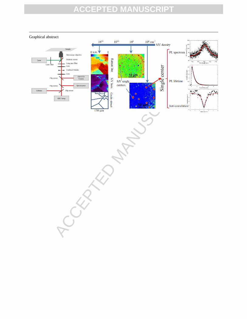
Graphical abstract
ACCEPTED MANUSCRIPT
ACCEP
TED M
ANUSC
RIPT
Optical properties of silicon-vacancy color centers in diamond created by ion implantation
and post-annealing
Highlights:
Single-photon SiV color centers created in diamond by ion implantation
Excellent spectral quality and reproducibility
Wide range of process parameters explored
Activation yield independent on implantation energy
Activation yield dependent on native defects concentration
ACCEPTED MANUSCRIPT