Embed Size (px)
Citation preview
This is a repository copy of Optical trapping with planar silicon metalenses.
White Rose Research Online URL for this paper:https://eprints.whiterose.ac.uk/134119/
Version: Accepted Version
Article:
Tkachenko, Georgiy, Stellinga, Daan, Ruskuc, Andrei et al. (3 more authors) (2018) Optical trapping with planar silicon metalenses. Optics Letters. pp. 3224-3227. ISSN 0146-9592
https://doi.org/10.1364/OL.43.003224
[email protected]://eprints.whiterose.ac.uk/
Reuse
Items deposited in White Rose Research Online are protected by copyright, with all rights reserved unless indicated otherwise. They may be downloaded and/or printed for private study, or other acts as permitted by national copyright laws. The publisher or other rights holders may allow further reproduction and re-use of the full text version. This is indicated by the licence information on the White Rose Research Online record for the item.
Takedown
If you consider content in White Rose Research Online to be in breach of UK law, please notify us by emailing [email protected] including the URL of the record and the reason for the withdrawal request.
Letter Optics Letters 1
Optical trapping with planar silicon metalenses
GEORGIY TKACHENKO1, DAAN STELLINGA2, ANDREI RUSKUC2,3, MINGZHOU CHEN1, KISHAN
DHOLAKIA1,*, AND THOMAS F. KRAUSS2
1SUPA, School of Physics and Astronomy, University of St. Andrews, KY16 9SS, UK2Department of Physics, University of York, Heslington, YO10 5DD, UK3California Institute of Technology, Pasadena, CA 91125, USA*Corresponding author: [email protected]
Compiled July 31, 2018
Contactless manipulation of micron-scale objects ina microfluidic environment is a key ingredient for arange of applications in the biosciences, including sort-ing, guiding and analysis of cells and bacteria. Opti-cal forces are powerful for this purpose but typicallyrequire bulky focusing elements to achieve the appro-priate optical field gradients. To this end, realizing thefocusing optics in a planar format would be very attrac-tive and conducive to integration of such microscaledevices either individually or as arrays. Here, we re-port on the first experimental demonstration of opticaltrapping in water using planar silicon metalenses illu-minated with a collimated laser beam. The structuresconsist of high-contrast gratings with a locally varyingperiod and duty-cycle. They are designed to mimicparabolic reflectors with a numerical aperture of 0.56at a vacuum wavelength of 1064 nm. We achieve bothtwo and three-dimensional trapping, with the latter re-alized by omitting the central Fresnel zones. The studyhighlights the versatility of such lithographically de-fined metastructures for exerting optical forces withoutthe need for traditional optical elements. © 2018 Optical
Society of America
OCIS codes: (140.7010) Laser trapping; (350.4855) Optical tweezers or
optical manipulation; (050.1950) Diffraction gratings.
http://dx.doi.org/10.1364/ol.XX.XXXXXX
Optical trapping of micron-sized objects with a single beamin 3D requires tight focusing of light, which can be achievedby optical elements with a high numerical aperture (NA) [1].Traditional glass lenses and microscope objectives are typicallyused to achieve such focusing, but they are bulky and cannot beeasily integrated into lab-on-a-chip systems, which are a primedomain for optical trapping aimed at micromanipulation andanalysis of cells and bacteria. An elegant solution to this problemhas been the use of submillimeter-size spherical lenses [2] orreflectors [3]. These have achieved NA = 0.96 and 3D opticaltrapping of polystyrene beads in a microfluidic environment.However, such optical elements are typically limited to sphericalshapes and thus are unable to generate anything other than
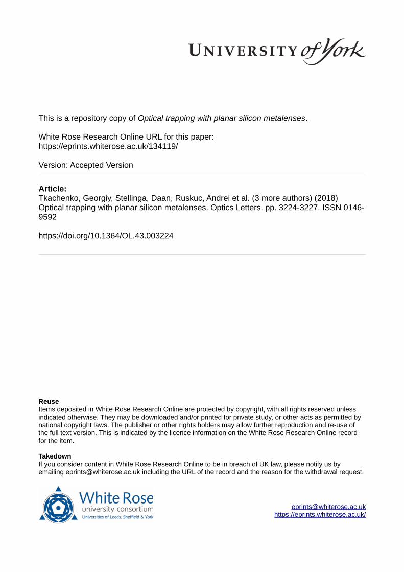
Fig. 1. (a) Principle of optical trapping with a planar metalens.(b) HCG in detail, where a is the local period, wr – the localridge width. (c) SEM micrograph of a fabricated metalenswhere light areas denote ridges, dark ones are grooves.
standard Gaussian beam traps. Moreover, they have significantrelief measuring hundreds of microns, which adds up to theform factor of the end device. In this context, one would wishfor an entirely planar structure capable of focusing light from acollimated incident beam into a tight spot, with the flexibilityof design and the prospect of generating traps with structuredbeams [4]. Naturally, a homogeneous flat surface cannot createthe required beam shaping, yet this task may be accomplishedwith metasurfaces [5–8] following the concept shown in Fig. 1(a).Realization of optical trapping with metasurface-based lenseshas been challenging because (i) the requirement to operate in afluid significantly limits the refractive index contrast and thusthe focusing efficiency; (ii) even though technically, the NA maybe high enough, the intensity of the high-angle beams at theperiphery of the lens is usually too low. In this Letter we reporton the first experimental demonstration of optical trapping withplanar metalenses.
In order to avoid spherical aberrations, which are detrimentalto optical trapping, particularly along the optical axis, a perfectmetalens with a focal distance f should have a parabolic phaseprofile
Φ(r) =2π
λ
(
√
r2 + f 2 − f
)
, (1)
where r is the distance from the center and λ is the operatingwavelength. Such a lens has NA(r) = n sin
(
tan−1(r/ f ))
withn being the refractive index of the medium.
Parabolic phase profiles can be created by a high-contrast grat-
Letter Optics Letters 2
ing (HCG) which is a metasurface with a subwavelength land-scape of alternating ridges and grooves on a planar substrate,see Fig. 1(b),(c). The function of such a grating is determinedby the interplay of guided modes with radiation modes [9]. Thephase map imposed by the HCG is defined by the spatial dis-tribution of the local period a and the duty cycle DC = wr/a,where wr is the local width of ridges. An HCG becomes a fullyfunctional beam shaping element when it can cover the fullphase range of 2π. Rigorous coupled wave analysis [10] allowsus to simulate the phase and efficiency (that is transmittance orreflectance, depending on the chosen operation mode) for allpossible combinations of a and DC. Subsequently, an optimumpath in the (a, DC) space has to be chosen so that the 2π phaserange could be covered with maximum net efficiency, see ourearlier work [11] for more details.
Previously, we have demonstrated planar metalenses mim-icking a parabolic reflector with NA reaching 0.93 [12]. However,optical trapping with such metalenses could not be achievedbecause of the low reflection efficiency in the high-order Fresnelzones, which are indispensable for the tight focusing of light.Indeed, the higher the order, the narrower the correspondingzone, as one can see in Fig. 1(c). At some point, the gratingdiscretization becomes comparable with the Fresnel zone width,and consequently the reflection efficiency for high r/ f decreasesdramatically. To overcome this problem, we have now imple-mented a boundary condition to the design of the path in the(a, DC) space, namely that each Fresnel zone must be repre-sented by at least three grating periods, the number of periodsbeing defined as
N =1
a
(
r −
√
(
r2 + λ2 − 2λ√
r2 + f 2
)
)
, (2)
where a is the average period for the chosen path. Eq.2 is de-livered from Eq. 1 by expressing the phase change for a Fresnelzone located at the radius r as Φ(r)− Φ(r − Na) = 2π. Sincewe expect planar metalenses to be applied for optical trappingin a microfluidic environment, we specifically designed them foroperation in water (n ≈ 1.33) at the widely used free-space wave-length λ = 1064 nm. The gratings are fabricated by direct-writeelectron beam lithography from a sub-micron film of crystallinesilicon bonded to a glass substrate, using the same process asin [12]. For a metalens operating in reflection at normal incidenceand in TM polarization (having electric field perpendicular tothe grating lines), the optimum path in the (a, DC) space corre-sponds to a ≈ 0.64 µm and a silicon film thickness of 0.38 µm.When the above mentioned boundary condition N ≥ 3 is stipu-lated, the NA of a metalens is limited to approximately 0.6. Inpractice, we have chosen a lens size of 100 µm × 100 µm and afocal length of f = 108 µm corresponding to NA ≈ 0.56.
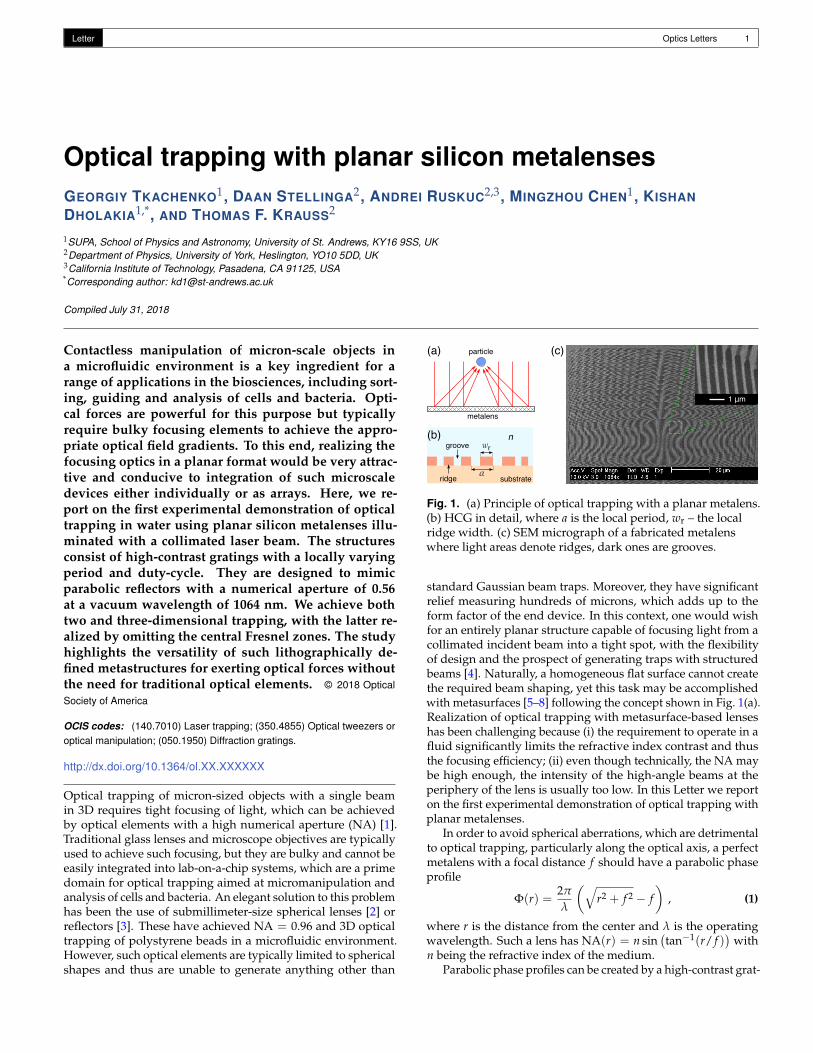
The focal spots created by the metalenses are characterizedusing an optical setup shown in Fig. 2(a). After being deflectedby a shortpass dichroic mirror (DM, Thorlabs DMSP 1000R), acollimated Gaussian beam (’input beam’) from a fiber laser (IPGPhotonics, cw at λ =1064 nm, beam diameter 5 mm) is relayedto the sample plane in order to coaxially illuminate a singlemetalens at normal incidence. The relay telescope consisting ofa biconvex lens (L, focal length 75 mm) and a water immersionmicroscope objective (MO, Nikon Fluor 60×/1.00W) reducesthe beam diameter to 130 µm. The focal plane of the objectivecoincides with that of the metalens. The light focused by themetalens is collected and imaged by means of a camera (C, Baslerpilot piA640-210gm) located at the back focal plane of lens L.
0
1
0.2
0.4
0.6
0.8
0 2-2 -1 1
Inte
nsity (
a. u.)
Inte
nsity (
a. u.)
0 2-2x (μm)
-10
-5
0
5
10
Δz (μm
)
Experiment Simulation
0 2-2x, y (μm)
-10
-5
0
5
10
(b)
0
1
0.2
0.4
0.6
0.8
0-4 8
x, y (μm)
Δz (μm)
(c) (d)
(e)
(a)
TM
inputbeam
L
FP
MO
metalenses
water
CFP
FP
DM
P
xy
z
0 2-2x (μm)
0 2-2y (μm)
y (μm
)
-2 -2
0 0
2 2
-8 4
0
1
Inte
nsity (
a. u.)
Fig. 2. Focal spot characterization. (a) Optical setup; dashedlines indicate the focal planes (FP). (b) Optical image of a met-alens; the arrow shows the incident electric field orientationfor TM polarization. (c) Sample transverse and axial intensityprofiles of the focal spot; the color bar is common. (d),(e) Nor-malized intensity profiles measured (dots) and simulated(solid curve) in the transverse ((d), at ∆z = 0) and axial ((e),at x = y = 0) cross sections of the focal spot. Grey areas de-note the standard deviation ranges of the experimental data.
The linear polarizer (P) sets the input beam to either TE or TMpolarization, the latter being indicated by the arrow in Fig. 2(b).
Each focal spot is considered in the Cartesian coordinateframe (x, y, z) with z indicating the propagation direction of thereflected light and the metalens located in the z = 0 plane. Thecamera is displaced along z covering the 80 µm long distancecentered on z = f . Fig. 2(c, top left) depicts the camera imagewith the maximum intensity level (captured at z ≈ f ). Fig. 2(c,bottom left) is the a sample intensity map compiled from thecamera images at the axial locations ∆z = z − f . We simulatethe electric field distribution at the focal spot by means of theRayleigh-Sommerfeld diffraction integral with the initial phasefront Φ(r) described by Eq. 1, where r2 = x2 + y2. The simulatedtransverse (at ∆z = 0) and axial (at y = 0) intensity profiles arepresented in Fig. 2(c, right).
We have characterized eight different metalenses for bothTE and TM polarization states. The measured transverse andaxial profiles of the focal spots in each case are summarized inFigs. 2(d, e). We found that normalized intensity profiles did notdepend on the polarization. We attribute the asymmetry of themeasured axial profiles (Fig. 2(e)) to the spherical aberrations inthe imaging system. The simulated beam waist radius (obtainedby fitting to a Gaussian distribution) at ∆z = 0 equals 0.67 µm,which is within the confidence range of the measured beamwaist radius equal to 0.66 ± 0.05 µm. We note that a high-NAlens is commonly characterized by the Airy disc radius (whichequals 0.95 for the simulated curve in Fig. 2(d)). However, sincethe function of metalenses in this work is not to image but totrap particles, treating the focal spot as a Gaussian beam is morerelevant for the following reasons. First, position fluctuationsof a particle around an optical trap are usually 1-2 orders ofmagnitude smaller than fluctuations of the beam size, thus thestructure of the Airy diffraction pattern beyond the full width athalf-maximum is not important in the context of optical manipu-lation. The second reason is related to the power measurementsdescribed below.
In addition to characterising the focal spot, the camera im-
Letter Optics Letters 3
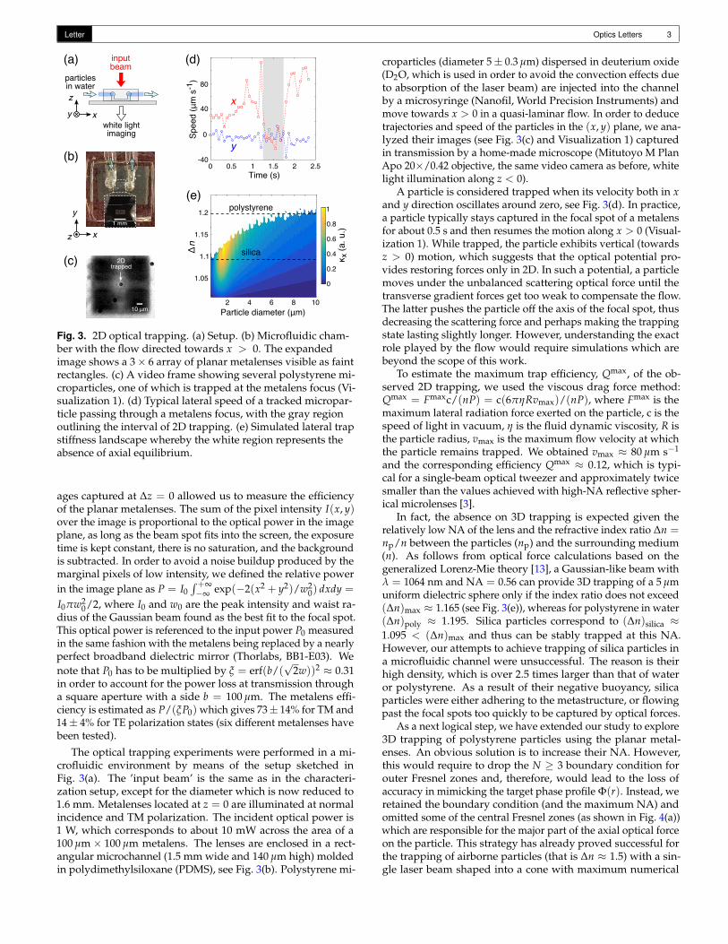
Fig. 3. 2D optical trapping. (a) Setup. (b) Microfluidic cham-ber with the flow directed towards x > 0. The expandedimage shows a 3 × 6 array of planar metalenses visible as faintrectangles. (c) A video frame showing several polystyrene mi-croparticles, one of which is trapped at the metalens focus (Vi-sualization 1). (d) Typical lateral speed of a tracked micropar-ticle passing through a metalens focus, with the gray regionoutlining the interval of 2D trapping. (e) Simulated lateral trapstiffness landscape whereby the white region represents theabsence of axial equilibrium.
ages captured at ∆z = 0 allowed us to measure the efficiencyof the planar metalenses. The sum of the pixel intensity I(x, y)over the image is proportional to the optical power in the imageplane, as long as the beam spot fits into the screen, the exposuretime is kept constant, there is no saturation, and the backgroundis subtracted. In order to avoid a noise buildup produced by themarginal pixels of low intensity, we defined the relative power
in the image plane as P = I0
∫ +∞
−∞exp(−2(x2 + y2)/w2
0) dxdy =
I0πw20/2, where I0 and w0 are the peak intensity and waist ra-
dius of the Gaussian beam found as the best fit to the focal spot.This optical power is referenced to the input power P0 measuredin the same fashion with the metalens being replaced by a nearlyperfect broadband dielectric mirror (Thorlabs, BB1-E03). We
note that P0 has to be multiplied by ξ = erf(b/(√
2w))2 ≈ 0.31in order to account for the power loss at transmission througha square aperture with a side b = 100 µm. The metalens effi-ciency is estimated as P/(ξP0) which gives 73± 14% for TM and14 ± 4% for TE polarization states (six different metalenses havebeen tested).
The optical trapping experiments were performed in a mi-crofluidic environment by means of the setup sketched inFig. 3(a). The ’input beam’ is the same as in the characteri-zation setup, except for the diameter which is now reduced to1.6 mm. Metalenses located at z = 0 are illuminated at normalincidence and TM polarization. The incident optical power is1 W, which corresponds to about 10 mW across the area of a100 µm × 100 µm metalens. The lenses are enclosed in a rect-angular microchannel (1.5 mm wide and 140 µm high) moldedin polydimethylsiloxane (PDMS), see Fig. 3(b). Polystyrene mi-
croparticles (diameter 5 ± 0.3 µm) dispersed in deuterium oxide(D2O, which is used in order to avoid the convection effects dueto absorption of the laser beam) are injected into the channelby a microsyringe (Nanofil, World Precision Instruments) andmove towards x > 0 in a quasi-laminar flow. In order to deducetrajectories and speed of the particles in the (x, y) plane, we ana-lyzed their images (see Fig. 3(c) and Visualization 1) capturedin transmission by a home-made microscope (Mitutoyo M PlanApo 20×/0.42 objective, the same video camera as before, whitelight illumination along z < 0).
A particle is considered trapped when its velocity both in xand y direction oscillates around zero, see Fig. 3(d). In practice,a particle typically stays captured in the focal spot of a metalensfor about 0.5 s and then resumes the motion along x > 0 (Visual-ization 1). While trapped, the particle exhibits vertical (towardsz > 0) motion, which suggests that the optical potential pro-vides restoring forces only in 2D. In such a potential, a particlemoves under the unbalanced scattering optical force until thetransverse gradient forces get too weak to compensate the flow.The latter pushes the particle off the axis of the focal spot, thusdecreasing the scattering force and perhaps making the trappingstate lasting slightly longer. However, understanding the exactrole played by the flow would require simulations which arebeyond the scope of this work.
To estimate the maximum trap efficiency, Qmax, of the ob-served 2D trapping, we used the viscous drag force method:Qmax = Fmaxc/(nP) = c(6πηRvmax)/(nP), where Fmax is themaximum lateral radiation force exerted on the particle, c is thespeed of light in vacuum, η is the fluid dynamic viscosity, R isthe particle radius, vmax is the maximum flow velocity at whichthe particle remains trapped. We obtained vmax ≈ 80 µm s−1
and the corresponding efficiency Qmax ≈ 0.12, which is typi-cal for a single-beam optical tweezer and approximately twicesmaller than the values achieved with high-NA reflective spher-ical microlenses [3].
In fact, the absence on 3D trapping is expected given therelatively low NA of the lens and the refractive index ratio ∆n =np/n between the particles (np) and the surrounding medium(n). As follows from optical force calculations based on thegeneralized Lorenz-Mie theory [13], a Gaussian-like beam withλ = 1064 nm and NA = 0.56 can provide 3D trapping of a 5 µmuniform dielectric sphere only if the index ratio does not exceed(∆n)max ≈ 1.165 (see Fig. 3(e)), whereas for polystyrene in water(∆n)poly ≈ 1.195. Silica particles correspond to (∆n)silica ≈1.095 < (∆n)max and thus can be stably trapped at this NA.However, our attempts to achieve trapping of silica particles ina microfluidic channel were unsuccessful. The reason is theirhigh density, which is over 2.5 times larger than that of wateror polystyrene. As a result of their negative buoyancy, silicaparticles were either adhering to the metastructure, or flowingpast the focal spots too quickly to be captured by optical forces.
As a next logical step, we have extended our study to explore3D trapping of polystyrene particles using the planar metal-enses. An obvious solution is to increase their NA. However,this would require to drop the N ≥ 3 boundary condition forouter Fresnel zones and, therefore, would lead to the loss ofaccuracy in mimicking the target phase profile Φ(r). Instead, weretained the boundary condition (and the maximum NA) andomitted some of the central Fresnel zones (as shown in Fig. 4(a))which are responsible for the major part of the axial optical forceon the particle. This strategy has already proved successful forthe trapping of airborne particles (that is ∆n ≈ 1.5) with a sin-gle laser beam shaped into a cone with maximum numerical
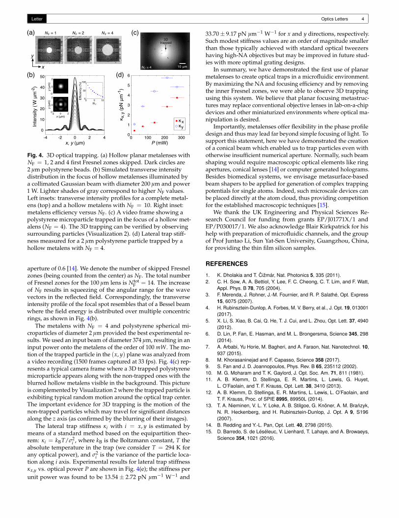
Letter Optics Letters 4
Fig. 4. 3D optical trapping. (a) Hollow planar metalenses withNF = 1, 2 and 4 first Fresnel zones skipped. Dark circles are2 µm polystyrene beads. (b) Simulated transverse intensitydistribution in the focus of hollow metalenses illuminated bya collimated Gaussian beam with diameter 200 µm and power1 W. Lighter shades of gray correspond to higher NF values.Left insets: transverse intensity profiles for a complete metal-ens (top) and a hollow metalens with NF = 10. Right inset:metalens efficiency versus NF. (c) A video frame showing apolystyrene microparticle trapped in the focus of a hollow met-alens (NF = 4). The 3D trapping can be verified by observingsurrounding particles (Visualization 2). (d) Lateral trap stiff-ness measured for a 2 µm polystyrene particle trapped by ahollow metalens with NF = 4.
aperture of 0.6 [14]. We denote the number of skipped Fresnelzones (being counted from the center) as NF. The total numberof Fresnel zones for the 100 µm lens is Ntot
F = 14. The increaseof NF results in squeezing of the angular range for the wavevectors in the reflected field. Correspondingly, the transverseintensity profile of the focal spot resembles that of a Bessel beamwhere the field energy is distributed over multiple concentricrings, as shown in Fig. 4(b).
The metalens with NF = 4 and polystyrene spherical mi-croparticles of diameter 2 µm provided the best experimental re-sults. We used an input beam of diameter 374 µm, resulting in aninput power onto the metalens of the order of 100 mW. The mo-tion of the trapped particle in the (x, y) plane was analyzed froma video recording (1500 frames captured at 33 fps). Fig. 4(c) rep-resents a typical camera frame where a 3D trapped polystyrenemicroparticle appears along with the non-trapped ones with theblurred hollow metalens visible in the background. This pictureis complemented by Visualization 2 where the trapped particle isexhibiting typical random motion around the optical trap center.The important evidence for 3D trapping is the motion of thenon-trapped particles which may travel for significant distancesalong the z axis (as confirmed by the blurring of their images).
The lateral trap stiffness κi with i = x, y is estimated bymeans of a standard method based on the equipartition theo-rem: κi = kBT/σ2
i , where kB is the Boltzmann constant, T theabsolute temperature in the trap (we consider T = 294 K forany optical power), and σ2
i is the variance of the particle loca-tion along i axis. Experimental results for lateral trap stiffnessκx,y vs. optical power P are shown in Fig. 4(e); the stiffness per
unit power was found to be 13.54 ± 2.72 pN µm−1 W−1 and
33.70 ± 9.17 pN µm−1 W−1 for x and y directions, respectively.Such modest stiffness values are an order of magnitude smallerthan those typically achieved with standard optical tweezershaving high-NA objectives but may be improved in future stud-ies with more optimal grating designs.
In summary, we have demonstrated the first use of planarmetalenses to create optical traps in a microfluidic environment.By maximizing the NA and focusing efficiency and by removingthe inner Fresnel zones, we were able to observe 3D trappingusing this system. We believe that planar focusing metastruc-tures may replace conventional objective lenses in lab-on-a-chipdevices and other miniaturized environments where optical ma-nipulation is desired.
Importantly, metalenses offer flexibility in the phase profiledesign and thus may lead far beyond simple focusing of light. Tosupport this statement, here we have demonstrated the creationof a conical beam which enabled us to trap particles even withotherwise insufficient numerical aperture. Normally, such beamshaping would require macroscopic optical elements like ringapertures, conical lenses [14] or computer generated holograms.Besides biomedical systems, we envisage metasurface-basedbeam shapers to be applied for generation of complex trappingpotentials for single atoms. Indeed, such microscale devices canbe placed directly at the atom cloud, thus providing competitionfor the established macroscopic techniques [15].
We thank the UK Engineering and Physical Sciences Re-search Council for funding from grants EP/J01771X/1 andEP/P030017/1. We also acknowledge Blair Kirkpatrick for hishelp with preparation of microfluidic channels, and the groupof Prof Juntao Li, Sun Yat-Sen University, Guangzhou, China,for providing the thin film silicon samples.
REFERENCES
1. K. Dholakia and T. Cižmár, Nat. Photonics 5, 335 (2011).
2. C. H. Sow, A. A. Bettiol, Y. Lee, F. C. Cheong, C. T. Lim, and F. Watt,
Appl. Phys. B 78, 705 (2004).
3. F. Merenda, J. Rohner, J.-M. Fournier, and R. P. Salathé, Opt. Express
15, 6075 (2007).
4. H. Rubinsztein-Dunlop, A. Forbes, M. V. Berry, et al., J. Opt. 19, 013001
(2017).
5. X. Li, S. Xiao, B. Cai, Q. He, T. J. Cui, and L. Zhou, Opt. Lett. 37, 4940
(2012).
6. D. Lin, P. Fan, E. Hasman, and M. L. Brongersma, Science 345, 298
(2014).
7. A. Arbabi, Yu Horie, M. Bagheri, and A. Faraon, Nat. Nanotechnol. 10,
937 (2015).
8. M. Khorasaninejad and F. Capasso, Science 358 (2017).
9. S. Fan and J. D. Joannopoulos, Phys. Rev. B 65, 235112 (2002).
10. M. G. Moharam and T. K. Gaylord, J. Opt. Soc. Am. 71, 811 (1981).
11. A. B. Klemm, D. Stellinga, E. R. Martins, L. Lewis, G. Huyet,
L. O’Faolain, and T. F. Krauss, Opt. Lett. 38, 3410 (2013).
12. A. B. Klemm, D. Stellinga, E. R. Martins, L. Lewis, L. O’Faolain, and
T. F. Krauss, Proc. of SPIE 8995, 89950L (2014).
13. T. A. Nieminen, V. L. Y. Loke, A. B. Stilgoe, G. Knöner, A. M. Branzyk,
N. R. Heckenberg, and H. Rubinsztein-Dunlop, J. Opt. A 9, S196
(2007).
14. B. Redding and Y.-L. Pan, Opt. Lett. 40, 2798 (2015).
15. D. Barredo, S. de Léséleuc, V. Lienhard, T. Lahaye, and A. Browaeys,
Science 354, 1021 (2016).


![Spoof Surface Plasmon based Planar THz Sensor System ......York, USA: Springer Verlag, 2007. [3] Wenjuan Zhang, Guiqiang Zhu, Liguo Sun, and Fujianng Lin, Trapping of surface plasmon](https://img.pdfslide.net/doc/110x75/60b6f424bada474e9b446a3f/spoof-surface-plasmon-based-planar-thz-sensor-system-york-usa-springer.jpg)