Embed Size (px)
Citation preview

i
Optically Generation of Rapidly Tunable Millimeter Wave Subcarrier Using
Microchip Lasers
A Thesis
Submitted to the Faculty
of
Drexel University
by
Yifei Li
in partial fulfillment of the
requirements for the degree
of
Doctor of Philosophy
May 2003

ii
© Copyright 2003 Yifei Li. All Rights Reserved

ii
Dedications
To my family
iii
Acknowledgements
First, I thank my thesis advisor, Dr. Peter R. Herczfeld, for his guidance, support,
and patience throughout my graduate study. His help for the writing is essential for the
completion of this thesis work. Secondly, I thank Dr. Samuel Goldwasser for his personal
support, friendship, and professional help in the research, without which this thesis work
would be less fruitful. Next, I like to thank Dr. Lorenzo Narducci. His help and guidance
are vital in my understanding of the laser physics and the completion of the theoretical
part of the thesis work. I also feel very obliged to the friendship and personal support
from Dr. Arye Rosen and Dr. Stewart D. Personick. I also wish to thank Dr. Linda
Mullen and Dr. Maja Bystrom for their support and helpful suggestions.
I am extremely grateful to my friends and colleagues here in the Center for the
Microwave/Lightwave engineering. I would like specially to thank Dr. Afshin Daryoush,
Mike Ermold, David Yoo, and Mohammad Tofighi for the helpful discussions and to
Renee Cohen for her extreme good will.
Finally, I would like to thank my family, for their support during this new step in
my life.

iv
Table of Contents
List of Tables ...............................................................................................................................................................vii
List of Figures.............................................................................................................................................................viii
Abstract...........................................................................................................................................................................xii
Chapter 1: Introduction............................................................................................................................................... 1
1.1 The goal of this research effort.......................................................................................1
1.2 Contributions ................................................................................................................1
1.3 Thesis organization .......................................................................................................2
Chapter 2: Background and review of literature................................................................................................ 4
2.1 Background and motivations ..........................................................................................4
2.1.1 Hybrid lidar/radar system........................................................................................4
2.1.2 Mm-wave fiber radio ..............................................................................................6
2.2 Review on mm-wave optical subcarrier generation ..........................................................8
2.3 A new approach of generating low noise, tunable mm-wave optical subcarrier ................19
2.3.1 Microchip lasers...................................................................................................20
2.3.2 Noise control techniques.......................................................................................22
2.4 Laser intracavity FM dynamics ....................................................................................23
2.4.1 Laser frequency switching ....................................................................................24
2.4.2 Laser FM oscillation .............................................................................................24
2.4.3. Summary on laser FM dynamics review................................................................27
2.5 The objectives of this thesis work.................................................................................28
Chapter 3: Dynamics of the tunable microchip laser ..................................................................................... 29
3.1 Problem identification .................................................................................................30
3.2 Problem formulation ...................................................................................................32
3.2.1 Modeling of components ......................................................................................34
v
3.2.2 Overall cavity formulation ....................................................................................39
3.2.3 Model representation and uniform field limit ..........................................................47
3.3 Linear dyanmic model.................................................................................................53
3.3.1 Linearized Maxwell-Bloch equations .....................................................................54
3.3.2 Closed-form solution in frequency domain .............................................................57
3.3.3 The transient characteristics of the laser response with frequency tuning..................60
3.4 Direct simulation and discussion ..................................................................................64
3.4.1 Dynamic response of the laser...............................................................................65
3.4.2 Laser dynamic behavior for different cavity parameters ..........................................75
3.4.3 Summary of laser response for varying voltage ramp and cavity parameters.............87
Chapter 4: Tunable transmitter design................................................................................................................. 89
4.1 DTMOT concept.........................................................................................................89
4.2 Transmitter single longitudinal mode operation .............................................................92
4.3 The microchip laser transmitter single spatial mode operation ..................................... 100
4.4 Laser tuning.............................................................................................................. 103
4.4.1 Electrical voltage tuning sensitivity ..................................................................... 103
4.4.2 Temperature tuning sensitivity ............................................................................ 104
4.4.3 Sensitivity to pump power tuning ........................................................................ 105
4.5 Laser transmitter characterization ............................................................................... 105
4.5.1 Laser threshold and efficiency............................................................................. 105
4.5.2 Microchip laser frequency tuning ........................................................................ 109
4.5.3 Mm-wave operation potential.............................................................................. 112
4.5.4 Microchip laser chirp rate testing......................................................................... 113
4.5.6 The free running phase noise of the tunable transmitter......................................... 117
4.6 Summary.................................................................................................................. 120
Chapter 5: Transmitter phase noise control subsystem................................................................................ 121
vi
5.1 Digital frequency synthesizer ..................................................................................... 121
5.1.1 Synthesizer subsystem phase noise ...................................................................... 122
5.1.2 Frequency modulation within digital synthesizer subsystem.................................. 124
5.2 The delay line optical frequency-locking loop............................................................. 125
5.2.1 OFLL operation principle ................................................................................... 126
5.2.2 OFLL implementation using a non-ideally balanced mixer.................................... 132
5.2.3 OFLL loop stability and the loop filter design ...................................................... 134
5.2.4 Design of the OFLL system using a single loop .................................................... 139
5.2.5 Multi-loop OFLLs.............................................................................................. 141
5.3 Noise control subsystem characterization.................................................................... 146
5.3.1 Digital synthesizer type noise control................................................................... 146
5.3.2 Delay line optical frequency locked loop characterization ..................................... 153
Chapter 6: Digital FM fiber radio downlink transmission.......................................................................... 160
6.1 Fiber radio downlink performance.............................................................................. 161
6.2 Digital FM fiber radio downlink experiment ............................................................... 162
6.3 FM fiber radio up link and basestation implementation issues ...................................... 167
6.5 Summary of fiber radio downlink testing .................................................................... 168
Chapter 7: Conclusions and recommendations for future work............................................................... 169
7.1 Conclusions .............................................................................................................. 169
7.2 Recommendations for the future work........................................................................ 171
List of References..................................................................................................................................................... 173
Appendix A: The closed-form solution of electro-optic section .............................................................. 177
Appendix B: Simulation method based on the direct integration of Maxwell-Bloch equation ..... 181
Appendix C: The derivation for fundamental mode cross section........................................................... 190
Appendix D: A new discriminator structure minimizing the AM to phase noise conversion........ 195
Vita ................................................................................................................................................................................ 197

vii
List of Tables
2.1 Performance goal for the tunable transmitter in various applications .......................... 8
2.2 Review of literature table on mm-wave generation technologies............................... 10
2.3 Comparisons between different mm-wave subcarrier generation techniques ............ 18
3.1 The components inside tunable microchip laser......................................................... 31
3.2 Field envelope equations, boundary and initial conditions, in each sub-sections of the laser cavity........................................................................................................ 38
3.3 Pertinent laser parameters for the simulation.............................................................. 65
3.4 Lser parameters for electro-optic section length simulation....................................... 76
3.5 Common parameters for gain linewidth simulation.................................................... 81
3.6 Parameters for total cavity length simulation ............................................................. 85
5.1 The advantage and disadvantages of the digital synthesizer approach..................... 124
5.2 The design objectives of a single loop OFLL........................................................... 139
5.3 The parameters for the components in the single loop OFLL .................................. 140
6.1 The digital FM fiber radio link parameters ............................................................... 163
viii
List of Figures
2.1 Hybrid CWFM lidar/radar system................................................................................ 5
2.2 Fiber radio downlink based on direct digital FM modulation ...................................... 7
2.3 A new approach for tunable mm-wave optical subcarrier generation........................ 20
3.1 The electro-optic tunable microchip laser................................................................... 30
3.2 A unidirectional ring cavity with electro-optic tunability........................................... 32
3.3 The electro-optic tunable laser formulation process................................................... 39
3.4 An ideal model of a lossless ring cavity under electro-optic modulation................... 46
3.5 Transformation characteristics of the gain medium.................................................... 59
3.6 The transfer function of laser dynamic system. .......................................................... 59
3.7 The flow diagram for simulation ................................................................................ 64
3.8 The laser response under a ramp signal comparable to the experimental value ......... 66
3.9 The lasing frequency and gain profile......................................................................... 68
3.10 The laser response under “moderate speed”, low voltage ramp signal..................... 69
3.11 The laser response under fast, low voltage ramp signal ........................................... 70
3.12 Frequency ripple observed under fast, low voltage tuning ....................................... 71
3.13 The laser response under high voltage moderate speed ramp................................... 72
3.14 The laser response under “very fast” ramp signal with high voltage ....................... 74
3.15 The laser FM response vs. different electro-optic section length............................. 77
3.16 The laser tuning sensitivity at steady state................................................................ 79
3.17 The maximum ripple magnitude as a function of the electro-optic section length... 79
3.18 The ripple decay time as a function of the electro-optic section length ................... 80
3.19 The laser FM response vs. different gain linewidth.................................................. 81

ix
3.20 The ripple decay time vs. the gain medium linewidth.............................................. 83
3.21 The steady state frequency tuning vs. the gain medium linewidth........................... 83
3.22 The laser FM response vs. different cavity lengths or round trip times ................... 85
4.1 The dynamically tunable millimeter wave optical transmitter structure .................... 89
4.2 The heterodyne transmitter implementation............................................................... 91
4.3 Multimode operation threshold vs. total cavity lengths and gain section length........ 95
4.4 Multimode operation threshold vs. frequency detuning and gain section length ....... 95
4.5 Multimode operation threshold vs. frequency detuning and total cavity length......... 96
4.6 The cavity structure where gap exist between the gain section and the mirror .......... 98
4.7 The multimode operation threshold vs. gap length and gain section length............... 98
4.8 The multi-mode operation threshold vs. gap length ( 0.2 ~0.4 mm) .......................... 99
4.9 The multi-mode operation threshold vs. gap length and frequency detuning............. 99
4.10 The conceptual laser cavity under the pump induced the thermal guiding and thermal expansion ............................................................................................ 100
4.11 Fundamental spatial mode radius vs. different pump power .................................. 101
4.12 The normalized spatial mode radius vs. different pump power level and spatial mode...................................................................................................... 102
4.13 The microchip laser threshold and slope efficiency characteristics........................ 106
4.14 Laser spectrum at 1063.6 nm.................................................................................. 107
4.15 A transverse mode beat tone captured by microwave spectrum analyzer. ............. 108
4.16. Voltage tuning sensitivity ...................................................................................... 110
4.17 The frequency of the two laser beat signal as a function of the temperature.......... 111
4.18 Two-microchip laser beat signal vs. pump power change. ..................................... 112
4.19 The optical spectrum of 120GHz subcarrier signal @ 1340 nm............................. 113
4.20 The microchip laser chirp rate measurement system.............................................. 115

x
4.21 The output characteristics of the frequency discriminator...................................... 116
4.22 Applied ramp signal (top) and the frequency response (bottom) ........................... 116
4.23 The laser phase noise measurement setup ............................................................... 117
4.24 The free running phase noise measurement ............................................................ 118
5.1 The digital frequency synthesizer ............................................................................. 122
5.2 Delay line optical frequency locked loop (OFLL).................................................... 125
5.3 OFLL system block diagram .................................................................................... 127
5.4 The OFLL implementation scheme with reduced AM to PM noise conversion...... 133
5.5 OFLL loop filter structure......................................................................................... 134
5.6 The performance of the loop filter with 1st order compensation .............................. 137
5.7 The performance of the loop filter with 2nd order compensation.............................. 138
5.8 OFLL system noise floor for different fiber delay lengths ....................................... 140
5.9 A multi- loop OFLL employ two loops ..................................................................... 142
5.10 The open loop response of the double loop OFLL at maximum stable gain. ......... 145
5.11 Stability of the multi- loop OFLL............................................................................ 145
5.12 The digital synthesizer phase noise control subsystem........................................... 148
5.13 The digital synthesizer phase noise spectrum of 8.447GHz................................... 149
5.14 The digital synthesizer phase noise vs. operation frequency.................................. 149
5.15 The experimental scheme for 40GHz operation based on the digital synthesizer phase noise control.................................................................................................. 150
5.16 Optical spectrum of 40GHz subcarrier signal......................................................... 151
5.17 Phase noise spectrum of the downconverted signal (14GHz) ................................ 151
5.18 The response of the digital synthesizer under direction modulation ...................... 152
5.19 The OFLL experimental setup ................................................................................ 155

xi
5.20 Phase noise spectrum of single loop OFLL at lower frequencies........................... 156
5.21 The OFLL output single spectrum at 37GHz ......................................................... 157
5.22 The OFLL phase noise measurement results at mm-wave frequencies.................. 158
6.1 The digital FM fiber radio experimental setup ......................................................... 163
6.2 The fiber radio downlink noise charactistics ............................................................ 164
6.3 The demodulation result captured by the HP VSA................................................... 165
6.4 The parasitic AM response ....................................................................................... 166
6.5 The baseband signal ringing ..................................................................................... 167
6.6 Fiber radio basestation.............................................................................................. 168
A.1 A separate E/O tuning section.................................................................................. 177
A.2 Coordinate transform from ( z~ ,t) plane to (u,v) plane ............................................. 178
B.1 Normalized time and space net to carry out the solution process. ........................... 184
B.2 The flow diagram for two dimension Euler method. ............................................... 185
B.3 The flow chart for the 2nd order two dimensional R-K method ............................... 189
C.1 The conceptual cavity structure under thermal guiding effect................................. 192

xii
Abstract Optically generation of rapidly tunable millimeter wave subcarriers using microchip
lasers Yifei Li
Peter R. Herczfeld, PhD
There is growing interest in applying photonic techniques to the generation of
high fidelity millimeter wave signals. This thesis concerns the optical domain generation
of rapidly tunable, very low noise millimeter wave subcarrier signals. Specifically, an
optical transmitter employing two heterodyned electro-optically tunable microchip lasers
has been designed, fabricated and characterized regarding its tuning range, speed, and
noise performance. To explain the fast tuning speed observed in the experiment, a
theoretical analysis of the laser dynamics during the intracavity frequency tuning process
is advanced using the semi-classic Maxwell-Bloch formulation. The theoretical analysis
confirms that microchip laser has a virtually unlimited tuning speed.
The output of the tunable transmitter is contaminated by the optical phase noise
initiating in the microchip laser. A novel phase noise control approach, coined an “optical
frequency locked loop” (OFLL), is developed to achieve low noise operation. Unlike
conventional techniques, this scheme utilizes a long fiber delay in place of an external
reference oscillator to correct the phase error. The optical frequency locked loop
outperforms conventional phased locks loops, particularly at higher millimeter wave
frequencies. The tunable transmitter was successfully evaluated in the context of a
broadband fiber radio downlink experiment.

i

1
Chapter 1: Introduction
1.1 The goal of this research effort
This thesis is concerned with a novel way of generating a fast dynamically
tunable millimeter wave (mm-wave) optical subcarrier for frequency chirped hybrid
lidar/radar and frequency modulated (FM) mm-wave fiber radio link applications.
Traditional mm-wave subcarrier techniques are limited by tunability and speed, which
affects the achievable resolution in hybrid lidar/radar and data rate of fiber radio links. In
response to these shortcomings, a dynamically tunable mm-wave optical transmitter,
which utilizes two heterodyned electro-optically tunable microchip lasers, is proposed,
implemented, and evaluated. A theoretical analysis of the laser FM dynamics is
performed to explain the rapid tuning speed obtained in the experiment. In order to obtain
a low noise mm-wave subcarrier signal throughout the transmitter tuning range, a phase
noise control system employing the fiber delay line as a frequency reference is proposed,
implemented and tested.
1.2 Contributions
The key contributions of this thesis work are as following:
• A theoretical model for the electro-optic tunable laser based on the
Maxwell-Bloch formulation was developed. Using on this model, we
found that the optical frequency is tuned instantly; however, frequency
ripples occur due to the non-uniformity of the laser cavity. Laser response
under intracavity frequency tuning was found to be a strong function of
the relative size of the tuning element. We proved numerically and

2
analytically that the appearance of ripples is a transient effect and the
ripple decay time is calculated analytically.
• A novel high-speed tunable mm-wave optical transmitter employing
electro-optically tunable microchip lasers was designed, implemented and
tested.
• A novel phase noise control scheme capable of achieving low noise
operation over a wide range of carrier frequencies from 0 to 40 GHz and
beyond, was proposed, implemented and tested. This achieved a
performance better than -108dBc/Hz @ 10kHz offset, at least 10dB better
than any other heterodyning system described in the literature.
• A fiber radio downlink transmission using a directly modulated tunable
mm-wave optical transmitter was performed for the first time with
promising results.
1.3 Thesis organization
The organization of this thesis is the following:
Chapter 2 addresses the background and reviews the literature on the mm-wave
optic subcarrier generation techniques. A new subcarrier generation approach using the
heterodyning of two or more electro-optic tunable microchip laser is proposed. Finally,
the existing works on the laser intracavity FM dynamics are examined.
Chapter 3 studies the dynamics during the microchip laser intracavity frequency
modulation. First, a formulation based on the semi-classic Maxwell-Bloch equations is
derived specifically for the electro-optic tunable laser cavity. In the formulation, the
effect of the electro-optical tuning is modeled as a perturbation on the boundary condition

3
of the laser system. Based on the formulation, the conditions for the uniform field limit or
single mode operation are addressed. For the case where the effective frequency tuning is
less than the gain linewidth, an approximate closed-form solution is derived to analyze
the transient behavior of the laser during frequency tuning and its final steady state.
Finally, a numerical simulation is performed to explore the speed limitations of the laser.
Chapter 4 investigates issues pertinent to the design, and performance
characterization of the dynamically tunable mm-wave optical transmitter including output
power, tuning range, tuning speed, and noise.
Chapter 5 examines two alternate schemes of the phase noise control, namely
digital synthesizer and the optical frequency locked loop (OFLL). The OFLL format is
explained using a system model. The issues regarding the achievable noise performance
of the OFLL, and its practical implementation are addressed. Finally, empirical results
are used to compare the performance of these two approaches.
Chapter 6 focuses on a practical application of the tunable mm-wave optical
transmitter in the context of a fiber-radio downlink.
4
Chapter 2: Background and review of literature
2.1 Background and motivations
Microwave and millimeter wave techniques are increasingly being adapted to
optical systems, such as hybrid lidar/radar and hybrid mm-wave wireless / fiber optic
communications. The motivation of this thesis work is to develop a low noise transmitter
that can deliver broadband, rapidly tunable mm-wave optical subcarrier signal for hybrid
lidar/radar, and for mm-wave fiber radio systems. In this subsection, we’ll first discuss
briefly the hybrid lidar/radar system and mm-wave fiber radio and explain why the
tunable mm-wave optic transmitter is an enabling technology for those applications. Next
we review the pertinent literature concerning optical domain generation of mm-waves
and introduce the notion of microchip lasers as potential sources for the generation of
high fidelity mm-wave signals. This chapter culminates in the precise definition of the
objectives of this thesis.
2.1.1 Hybrid lidar/radar system Since the late 1970s, a number of lidar systems have been developed for the
detection of underwater objects and for tumors in human tissues, as well as for aerial
turbulence. When these lidar systems are used to probe targets submerged in turbulent
media like ocean water and body tissues, the intense scattering (clutter) from the media
results in poor contrast for target identification [1]. One way of suppressing the clutter is
to use hybrid lidar/radar [1], in which a Q-switched optical pulse is modulated by a
microwave signal, which is later processed by a coherent radar receiver. This hybrid
approach is effective because the lidar clutter has a low pass transfer characteristic. Thus,

5
the clutter effect is reduced when signal processing is performed at microwave
frequencies, far above the clutter cutoff frequency.
However, this pulsed approach has limited resolution. In a pulsed lidar/radar
system, the resolution is given by 2/τδ ∆⋅= u , where u is the speed of light in the
medium and τ∆ is the pulse width. For example, a typical medical imaging system
requires a 2 mm resolution (equivalent to a ~20ps pulse width), which makes the radar
signal processing extremely difficult. In order to achieve such a high resolution, we
proposed employing continuous wave frequency modulation (CWFM) [2, 3, 4, 5]
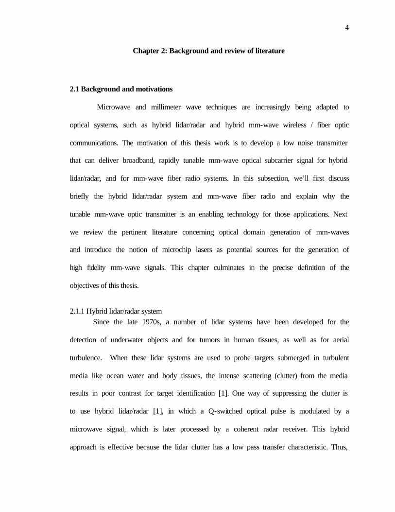
schemes in the hybrid lidar/radar system (see Figure 2.1). In this configuration, the
critical component is a rapidly tunable mm-wave optical transmitter, which sweeps the
mm-wave optical subcarrier frequency. The target distance is determined by the
frequency difference between the transmitted and returned signal.
Rapidly tunable mm- wave Optical
transmitter
Hspeed PD 1
Processor
Ramp Signal
t
V
Display
t
Freq
Transmitted signal
Reflected signal
τ
Hspeed PD 2
Figure 2.1: Hybrid CWFM lidar/radar system
6
As shown in Fig. 2.1, the hybrid lidar receiver only processes the low frequency
homodyne output signal from the mixer, which is easy compared with the pulsed system.
The resolution of this system is given by, ∆R=u/2∆F, where ∆F is frequency excursion.
In order to achieve 2 mm resolution, the excursion of the subcarrier frequency needs to be
at least 37 GHz.
This CWFM Lidar/Radar can also be used for free-space laser ranging, where the
target distance is much longer compared with biomedical imaging. The long target range
requires lower phase noise (narrower linewidth) to increase the coherent length of the
subcarrier signal.
Generation of a broadband tunable low noise mm-wave optical subcarrier for the
high-resolution hybrid lidar/radar systems is one of the motivations for this thesis work.
2.1.2 Mm-wave fiber radio Recently, there is interest in fiber radio systems [7, 8, 9, 10, 11, 12] for hybrid
wireless and fiber optic communications, in which a central station communicates with
one or more base stations via a fiber optic link (downlink), while traffic between the base
station and terminals within a local pico-cell uses mm-wave radio links. This hybrid
approach enjoys the advantages of both conventional wireless (convenience and
flexibility) and fiber optic (high bandwidth) communications systems. Inside existing
fiber radio system, the mm-wave subcarrier and data modulation are generated separately
and the data modulation format is limited to amplitude types, such as binary phase shift
keying (BPSK), quadrature amplitude modulation (QAM), and quadrature phase shift
keying (QPSK), etc. This results in complexity, but more importantly, incompatibility
with existing wireless systems that use continuous phase modulation (CPM) such as
7
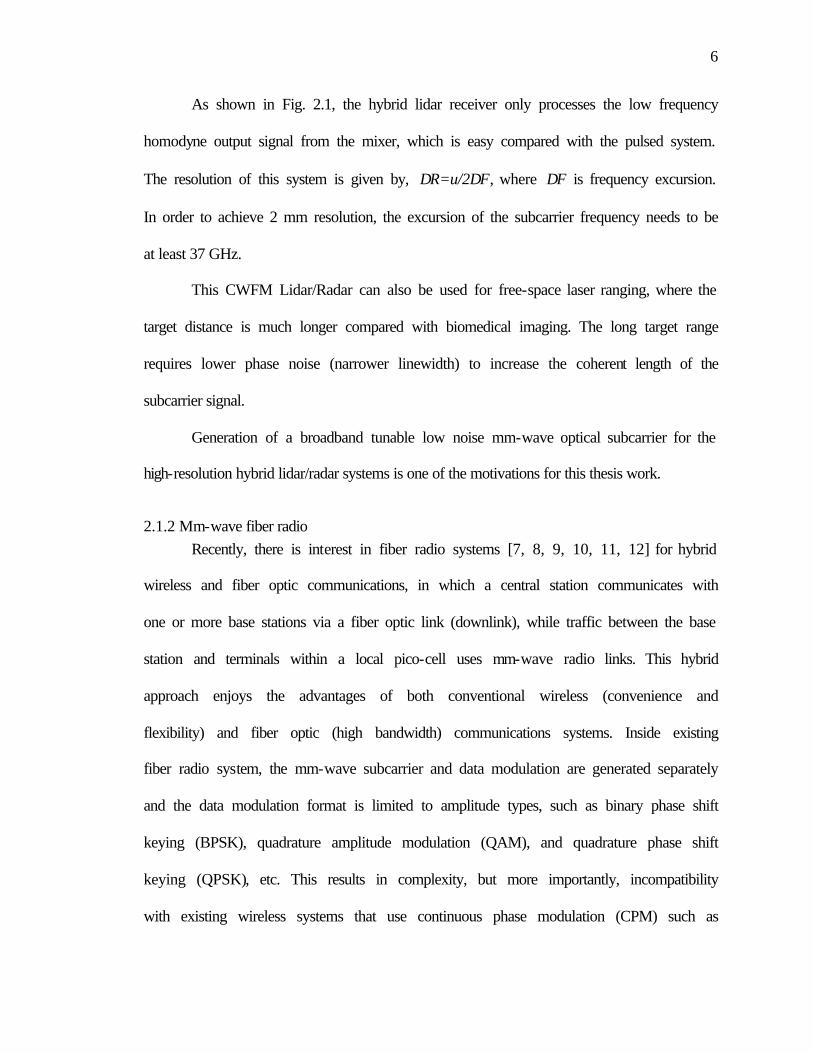
minimum shift keying (MSK). One solution to those problems is to use the digital FM
fiber radio link (figure 2.2) [13].
Information
Tunable mm-wave optical transmitter
Center Station
High speed PD
MSK receiver
Base Station
Figure 2.2: Fiber radio downlink based on direct digital FM modulation
In figure 2.2, the information bit directly modulates the frequency of mm-wave
subcarrier, and both a high quality mm-wave subcarrier and CPM-type digital signal are
generated simultaneously. The enabling component here is a tunable mm-wave optical
transmitter with high tuning sensitivity, high tuning speed, and low phase noise to assure
reliable, high data rate operation. The design and implementation of such a transmitter for
mm-wave fiber radio is the second concern of the thesis.
In conclusion, the key requirement for both the CWFM hybrid lidar/radar and
directly FM mm-wave fiber radio is a rapidly tunable mm-wave optical transmitter. The
transmitter should have a very wide tuning range (>37 GHz) for biomedical imaging, and
the low phase noise for the free space ranging. While in the fiber radio system, the
transmitter should be adopted to have high sensitivity, high tuning speed, and low phase
noise. Table 2.1 summarized the performance goals for the tunable transmitter for four
typical applications.

8
Table 2.1: Performance goal for the tunable transmitter in various applications
Applications Tuning range Power Wave-length
Tuning speed
Phase noise @10kHz offset
Biomedical imaging >37GHz >10mW 700~ 900nm
___ ___
Under water detection
>1GHz, depends on resolution requirement
>1W ~500nm ___
<-90dBc/Hz (depend on range)
Free space ranging >1GHz, depends on resolution requirement
>1W 1.06/ 1.5nm
___ <-90dBc/Hz (depend on range)
Digital FM fiber radio
>100MHz, depends on data rate
>1mW 1.06 /1.3/1.5 nm
>10GHz/µs < -90dBc/Hz
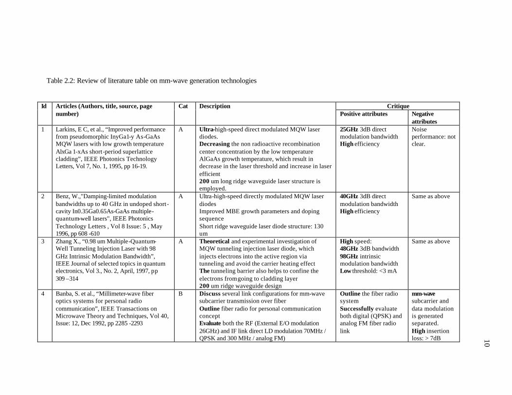
2.2 Review on mm-wave optical subcarrier generation
An extensive literature review has been performed on the existing mm-wave
optical subcarrier generation techniques. Approximately 120 papers on millimeter wave
subcarrier generation were searched and reviewed, from which the 40 most representative
papers are reviewed in detail with emphasis on the phase noise performance, tuning range
and tuning speed. The review is summarized in Table 2.2.
Most of the existing millimeter-wave optical subcarrier generation techniques fall
into the following six categories:
A. Direct modulation of a laser diode (LD)
B. External modulation of laser diode or other laser source
C. Resonance modulation
D. Laser mode locking
E. Injection locking

9
F. Lasers heterodyning
The comparison of these approaches for mm-wave optical subcarrier generation
techniques is summarized in Table 2.3. The examination of these methods suggests that
the preferred way of generation of a low noise, rapidly tunable mm-wave optical
subcarrier should be optical heterodyning of two laser sources with high spectral quality.
10
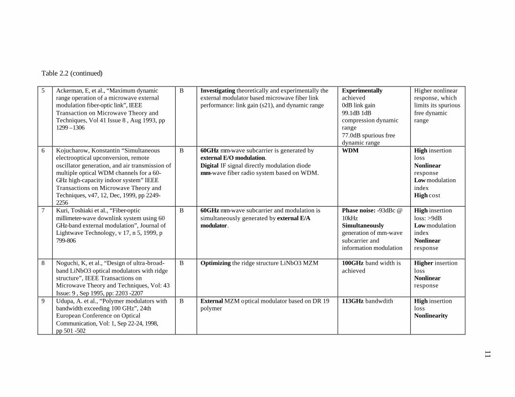
Table 2.2: Review of literature table on mm-wave generation technologies
Critique Id Articles (Authors, title, source, page
number) Cat Description
Positive attributes Negative attributes
1 Larkins, E C, et al., “Improved performance from pseudomorphic InyGa1-y As-GaAs MQW lasers with low growth temperature AlxGa 1-xAs short-period superlattice cladding”, IEEE Photonics Technology Letters, Vol 7, No. 1, 1995, pp 16-19.
A Ultra-high-speed direct modulated MQW laser diodes. Decreasing the non radioactive recombination center concentration by the low temperature AlGaAs growth temperature, which result in decrease in the laser threshold and increase in laser efficient 200 um long ridge waveguide laser structure is employed.
25GHz 3dB direct modulation bandwidth High efficiency
Noise performance: not clear.
2 Benz, W.,"Damping-limited modulation bandwidths up to 40 GHz in undoped short-cavity In0.35Ga0.65As-GaAs multiple-quantum-well lasers", IEEE Photonics Technology Letters , Vol 8 Issue: 5 , May 1996, pp 608 -610
A Ultra-high-speed directly modulated MQW laser diodes Improved MBE growth parameters and doping sequence Short ridge waveguide laser diode structure: 130 um
40GHz 3dB direct modulation bandwidth High efficiency
Same as above
3 Zhang X., “0.98 um Multiple-Quantum-Well Tunneling Injection Laser with 98 GHz Intrinsic Modulation Bandwidth”, IEEE Journal of selected topics in quantum electronics, Vol 3., No. 2, April, 1997, pp 309 –314
A Theoretical and experimental investigation of MQW tunneling injection laser diode, which injects electrons into the active region via tunneling and avoid the carrier heating effect The tunneling barrier also helps to confine the electrons from going to cladding layer 200 um ridge waveguide design
High speed: 48GHz 3dB bandwidth 98GHz intrinsic modulation bandwidth Low threshold: <3 mA
Same as above
4 Banba, S. et al., “Millimeter-wave fiber optics systems for personal radio communication”, IEEE Transactions on Microwave Theory and Techniques, Vol 40, Issue: 12, Dec 1992, pp 2285 -2293
B Discuss several link configurations for mm-wave subcarrier transmission over fiber Outline fiber radio for personal communication concept Evaluate both the RF (External E/O modulation 26GHz) and IF link direct LD modulation 70MHz / QPSK and 300 MHz / analog FM)
Outline the fiber radio system Successfully evaluate both digital (QPSK) and analog FM fiber radio link
mm-wave subcarrier and data modulation is generated separated. High insertion loss: > 7dB 10
11
Table 2.2 (continued) 5 Ackerman, E, et al., “Maximum dynamic
range operation of a microwave external modulation fiber-optic link”, IEEE Transaction on Microwave Theory and Techniques, Vol 41 Issue 8 , Aug 1993, pp 1299 –1306
B Investigating theoretically and experimentally the external modulator based microwave fiber link performance: link gain (s21), and dynamic range
Experimentally achieved 0dB link gain 99.1dB 1dB compression dynamic range 77.0dB spurious free dynamic range
Higher nonlinear response, which limits its spurious free dynamic range
6 Kojucharow, Konstantin “Simultaneous electrooptical upconversion, remote oscillator generation, and air transmission of multiple optical WDM channels for a 60-GHz high-capacity indoor system” IEEE Transactions on Microwave Theory and Techniques, v47, 12, Dec, 1999, pp 2249-2256
B 60GHz mm-wave subcarrier is generated by external E/O modulation. Digital IF signal directly modulation diode mm-wave fiber radio system based on WDM.
WDM
High insertion loss Nonlinear response Low modulation index High cost
7 Kuri, Toshiaki et al., “Fiber-optic millimeter-wave downlink system using 60 GHz-band external modulation”, Journal of Lightwave Technology, v 17, n 5, 1999, p 799-806
B 60GHz mm-wave subcarrier and modulation is simultaneously generated by external E/A modulator.
Phase noise: -93dBc @ 10kHz Simultaneously generation of mm-wave subcarrier and information modulation
High insertion loss: >9dB Low modulation index Nonlinear response
8 Noguchi, K, et al., “Design of ultra-broad-band LiNbO3 optical modulators with ridge structure”, IEEE Transactions on Microwave Theory and Techniques, Vol: 43 Issue: 9 , Sep 1995, pp: 2203 -2207
B Optimizing the ridge structure LiNbO3 MZM 100GHz band width is achieved
Higher insertion loss Nonlinear response
9 Udupa, A. et al., “Polymer modulators with bandwidth exceeding 100 GHz”, 24th European Conference on Optical Communication, Vol: 1, Sep 22-24, 1998, pp 501 -502
B External MZM optical modulator based on DR 19 polymer
113GHz bandwdith High insertion loss Nonlinearity
11

12
Table 2.2 (continued) 10
Georges, John B, et al., “Multichannel millimeter wave subcarrier transmission by resonant modulation of monolithic semiconductor lasers” IEEE PLT, v7, 4, Apr, 1995, p 431-433
C mm-wave subcarrier and information modulation is generated simultaneously by resonance modulation Resonance modulation bandwidth, and system dynamic range is investigated experimentally
Simultaneous generation of 40GHz subcarrier and signal modulation (~5MHz) Simplicity
Narrow bandwidth: <5MHz Non-flat response
11 Georges, John B, et al., “Optical transmission of narrowband millimeter-wave signals” IEEE Transactions on Microwave Theory and Techniques, v43, 9/2, Sept, 1995, p 2229-2240
C, E
Compare three schemes of digital signal modulated mm-wave subcarrier generation: LD resonance modulation LD heterodyning with feed-forward modulation Passive mode locking with PLL stabilization
LD heterodyning: higher tuning range: 100 GHz. Feedforward modulation: easy to implement for 1MHz linewidth LD Passive mode locking with PLL: phase noise: ~100dBc @100Khz offset
Resonance modulation: narrow bandwidth LD heterodyne: complexity. Passive mode locking: no tunability, narrorw bandwidth (<10MHz)
12 Ohno, Tetsuichiro, et al. “Application of DBR mode-locked lasers in millimeter-wave fiber-radio system”, IEEE Journal of Lightwave Technology, v18, 1, Jan, 2000, p 44-49
D 40GHz mm-wave subcarrier generation by 4-modes DBR LD AM Mode locking Reduce dispersion penalty by fiber grading filter
Good phase noise: -109 dBc/Hz @100Khz offset Low insertion loss
No tunability Intensity noise
13 Ahmed, Z, et al., “Locking characteristics of a passively mode-locked monolithic DBR laser stabilized by optical injection”, IEEE Photonics Technology Letters, Vol 8 Issue 1 , Jan 1996, pp 37 –39
D, E Using optical injection locking to stabilized passive mode locked laser diode 37GHz mm-wave subcarrier is generated
With optical injection locking the phase noise decreased by 20dB (from –67dBc/Hz @ 1MHz to –87dBc/Hz @ 1MHz)
Less ideal phase noise performance
14 Kuri, T, et al., “Long-term stabilized millimeter-wave generation using a high-power mode-locked laser diode module”, IEEE Transactions on Microwave Theory and Techniques, Vol 47 Issue: 5, May 1999, pp: 570 –574
D, E Passive mode locked is stabilized by optical injection locking 60GHz mm-wave subcarrier is generated
Thefrequency stability of the 60GHz carrier is within 50Hz over 1500 hour period
No phase noise measurement
12
13
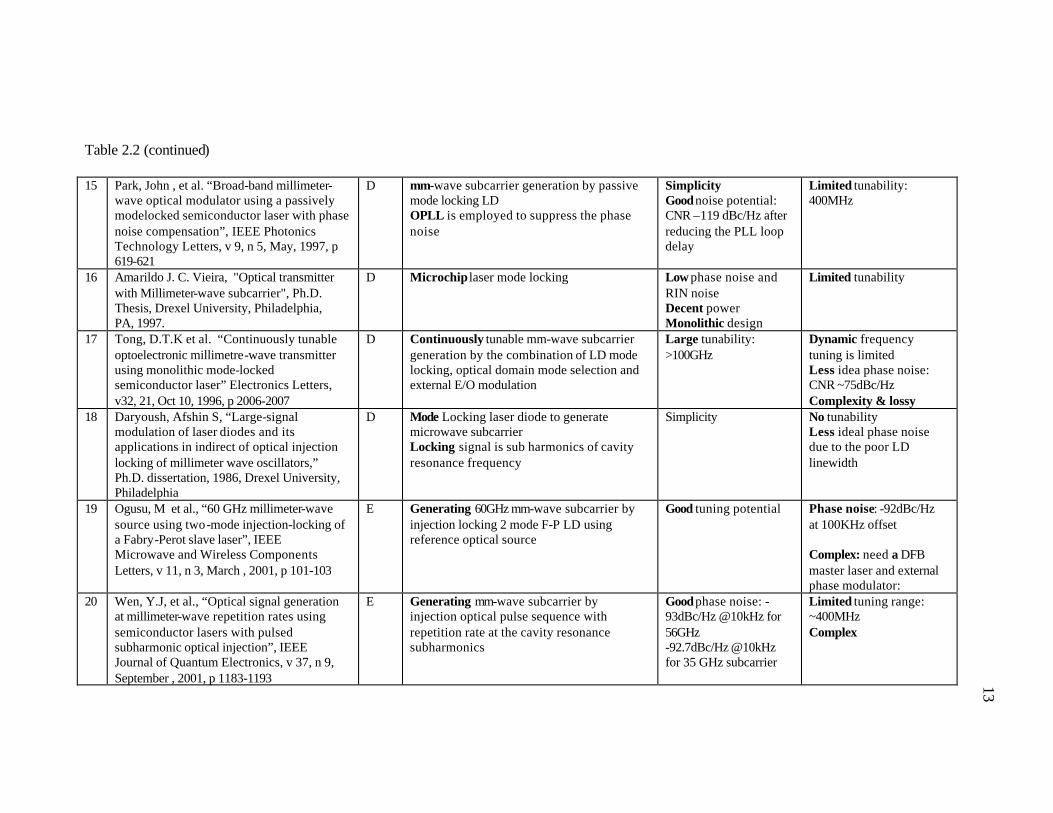
Table 2.2 (continued) 15 Park, John , et al. “Broad-band millimeter-
wave optical modulator using a passively modelocked semiconductor laser with phase noise compensation”, IEEE Photonics Technology Letters, v 9, n 5, May, 1997, p 619-621
D mm-wave subcarrier generation by passive mode locking LD OPLL is employed to suppress the phase noise
Simplicity Good noise potential: CNR –119 dBc/Hz after reducing the PLL loop delay
Limited tunability: 400MHz
16 Amarildo J. C. Vieira, "Optical transmitter with Millimeter-wave subcarrier", Ph.D. Thesis, Drexel University, Philadelphia, PA, 1997.
D Microchip laser mode locking Low phase noise and RIN noise Decent power Monolithic design
Limited tunability
17 Tong, D.T.K et al. “Continuously tunable optoelectronic millimetre-wave transmitter using monolithic mode-locked semiconductor laser” Electronics Letters, v32, 21, Oct 10, 1996, p 2006-2007
D Continuously tunable mm-wave subcarrier generation by the combination of LD mode locking, optical domain mode selection and external E/O modulation
Large tunability: >100GHz
Dynamic frequency tuning is limited Less idea phase noise: CNR ~75dBc/Hz Complexity & lossy
18 Daryoush, Afshin S, “Large-signal modulation of laser diodes and its applications in indirect of optical injection locking of millimeter wave oscillators,” Ph.D. dissertation, 1986, Drexel University, Philadelphia
D Mode Locking laser diode to generate microwave subcarrier Locking signal is sub harmonics of cavity resonance frequency
Simplicity
No tunability Less ideal phase noise due to the poor LD linewidth
19 Ogusu, M et al., “60 GHz millimeter-wave source using two-mode injection-locking of a Fabry-Perot slave laser”, IEEE Microwave and Wireless Components Letters, v 11, n 3, March , 2001, p 101-103
E Generating 60GHz mm-wave subcarrier by injection locking 2 mode F-P LD using reference optical source
Good tuning potential Phase noise: -92dBc/Hz at 100KHz offset Complex: need a DFB master laser and external phase modulator:
20 Wen, Y.J, et al., “Optical signal generation at millimeter-wave repetition rates using semiconductor lasers with pulsed subharmonic optical injection”, IEEE Journal of Quantum Electronics, v 37, n 9, September , 2001, p 1183-1193
E Generating mm-wave subcarrier by injection optical pulse sequence with repetition rate at the cavity resonance subharmonics
Good phase noise: -93dBc/Hz @10kHz for 56GHz -92.7dBc/Hz @10kHz for 35 GHz subcarrier
Limited tuning range: ~400MHz Complex
13

14
Table 2.2 (continued) 21 Fukushima, S, et al., “Optoelectronic
synthesis of milliwatt-level multi-octave millimeter-wave signals using an optical frequency comb generator and a unitraveling-carrier photodiode”, IEEE Photonics Technology Letters, v 13, n 7, July , 2001, p 720-722
E Generating injection source by optical comb Two frequency components are selected from the optical comb and injected to two tunable laser diodes
Very broad tuning range: 10 ~ 60GHz
Less ideal phase noise: ~67dBC/Hz @ 100Khz for 60GHz carrier Complex
22 *
Hong, Jin, et al., “Tunable millimeter-wave generation with sub harmonic injection locking in two-section strongly gain-coupled DFB lasers”, IEEE PLT, v12, 5, 2000, p 543-545
E Injection locking (/mode locking) two modes of strongly gain coupled dual mode LD by sub harmonics of the mode spacing The mode spacing is controlled by the bias current
Tunable: mode spacing can be varied from: 18 to 40GHz, indicating 22 GHz tuning range Linewidth: <30Hz
Lack dynamic tunability Need tunable reference source
23 Ralf Peter Braun, et al., “Optical microwave generation and transmission experiments in the 12- and 60-GHz region for wireless communications”, IEEE Transactions on Microwave Theory and Techniques, Vol 46 Issue: 4 , Apr 1998, pp 320 -330
E, F 60GHz FM fiber radio link based on two LDs heterodyning is evaluated. Discussion on two multi-carrier fiber radio schemes:
• Three LDs heterodyning • Heterodyning a mode locked laser
with reference diode laser • 62GHz MM-wave subcarrier
generation by injection-locking the side bands of a mode locked laser diode source.
Evaluated novel FM fiber radio link, in which signal modulation and mm-wave carrier is simultaneously generated. Laser diode FM has higher FM index. Tunable: > 110GHz Demonstrating a PIC for two laser heterodyning Phase noise: -55dBc @ 100Hz
Laser diode has higher phase noise Phase locking scheme is complicated
24 Ka-Suen Lee, et al., “Generation of optical millimeter-wave with a widely tunable carrier using Fabry-Perot grating-lens external cavity laser”, IEEE Microwave and Guided Wave Letters, Vol: 9, Issue: 5, May 1999, pp: 192 –194
F Heterodyning two longitudinal modes of a FP grating – lens external cavity laser to generate 119GHz mm-wave subcarrier Using grating to adjust wavelength
> 60 nm wavelength tuning
No phase noise control
14

15
Table 2.2 (continued)
25 Wake, D, et al., “Optical generation of millimeter-wave signals for fiber-radio systems using a dual-mode DFB semiconductor laser Davies”, IEEE Transactions on Microwave Theory and Techniques, Vol: 43 Issue: 9 , Sep 1995, pp 2270 –2276
E Injection locking (mode locking) dual mode laser diode
Generating 60GHz & 40GHz mm-wave subcarrier Phase noise: -85dBc/Hz @ 10kHz offset
Narrowband Not tunable
26 Wis e, F.W. et al., “Low phase noise 33-40-GHz signal generation using multilaser phase-locked loops”, IEEE Photonics Technology Letters , Vol: 10 Issue: 9 , Sep 1998, pp: 1304 –1306
F Three external cavity LDs heterodyning Generates two subcarriers simultaneously Integrated phase noise (0 to 25MHz offset range): 0.01 rad rms
No tuning mechanism is mentioned.
27 Matsuura, Shuji, et al., “Tunable cavity-locked diode laser source for terahertz photomixing”, IEEE Transactions on Microwave Theory and Techniques, v48, 3, 2000, p 380-387
F THz signal generation by laser diode heterodyning Using high finesse F-P cavity as the frequency reference
No electronic reference Terahertz signal range signal
Noisy Linewidth <=1MHz
28 Simonis G. J. et al., “Optical Generation, Distribution, and control of Microwaves Using Laser Heterodyne”, IEEE Trans. MTT, vol. 38, No. 5, pp. 667-669, May, 1990.
F mm-wave subcarrier generation by direct heterodyning using low noise solid state laser No locking mechanism is employed
Dc to 52GHz tuning range Noise: -115dBc/Hz @ 300KHz offset
Slow tuning speed: temperature tuning Continuous tuning range limited by laser FSR
29 Ramos R. T., A. J. Seeds, " Delay, Linewidth and bandwidth limitations in optical phase-locked loop design", Electronic Letters, vol. 26, pp. 389-390, March 1990.
F Analysis on linewidth limitation on optical PLL for LD heterodyning
Investigating the laser linewidth vs. the allowed PLL loop delay
Poor linwidth of LD makes the PLL implementation difficult
30
Doi, Y. et al.; “Frequency stabilization of millimeter-wave subcarrier using laser heterodyne source and optical delay line” IEEE Photonics Technology Letters, v 13, n 9, September, 2001, p 1002-1004
F LD heterodyning stabilized by frequency discriminator structure
No need for external reference signal Potentially 100GHz tuning
Phase noise: very poor
15
16
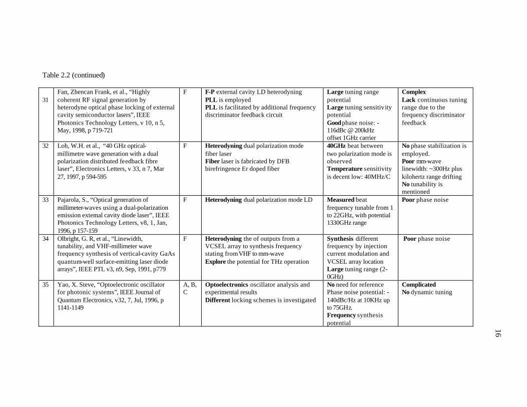
Table 2.2 (continued) 31
Fan, Zhencan Frank, et al., “Highly coherent RF signal generation by heterodyne optical phase locking of external cavity semiconductor lasers”, IEEE Photonics Technology Letters, v 10, n 5, May, 1998, p 719-721
F F-P external cavity LD heterodyning PLL is employed PLL is facilitated by additional frequency discriminator feedback circuit
Large tuning range potential Large tuning sensitivity potential Good phase noise: -116dBc @ 200kHz offset 1GHz carrier
Complex Lack continuous tuning range due to the frequency discriminator feedback
32 Loh, W.H. et al., “40 GHz optical-millimetre wave generation with a dual polarization distributed feedback fibre laser”, Electronics Letters, v 33, n 7, Mar 27, 1997, p 594-595
F Heterodyning dual polarization mode fiber laser Fiber laser is fabricated by DFB birefringence Er doped fiber
40GHz beat between two polarization mode is observed Temperature sensitivity is decent low: 40MHz/C
No phase stabilization is employed. Poor mm-wave linewidth: ~300Hz plus kilohertz range drifting No tunability is mentioned
33 Pajarola, S., “Optical generation of millimeter-waves using a dual-polarization emission external cavity diode laser”, IEEE Photonics Technology Letters, v8, 1, Jan, 1996, p 157-159
F Heterodyning dual polarization mode LD Measured beat frequency tunable from 1 to 22GHz, with potential 1330GHz range
Poor phase noise
34 Olbright, G. R, et al., “Linewidth, tunability, and VHF-millimeter wave frequency synthesis of vertical-cavity GaAs quantum-well surface-emitting laser diode arrays”, IEEE PTL v3, n9, Sep, 1991, p779
F Heterodyning the of outputs from a VCSEL array to synthesis frequency stating from VHF to mm-wave Explore the potential for THz operation
Synthesis different frequency by injection current modulation and VCSEL array location Large tuning range (2-0GHz)
Poor phase noise
35 Yao, X. Steve, “Optoelectronic oscillator for photonic systems”, IEEE Journal of Quantum Electronics, v32, 7, Jul, 1996, p 1141-1149
A, B, C
Optoelectronics oscillator analysis and experimental results Different locking schemes is investigated
No need for reference Phase noise potential: -140dBc/Hz at 10KHz up to 75GHz. Frequency synthesis potential
Complicated No dynamic tuning
16

17
Table 2.2 (continued)
36 Yao, et al., “Multiloop optoelectronic oscillator”, IEEE Journal of Quantum Electronics, Vol 36 Issue: 1 , Jan 2000, pp: 79 –84
B Multi loop OEO: the first loop for the resonator, and the second on for frequency selection Presenting a carrier suppression schemes based on the fiber delay line frequency discriminator for further phase noise suppression
Employing multi-loops Measured phase noise: -140dBc/Hz @ 10kHz for 10GHz carrier
Same as above
37 Davidson, T, et al., “High spectral purity CW oscillation and pulse generation in optoelectronic microwave oscillator”, Electronics Letters, v 35, n 15, 1999, p 1260-1261
B Optoelectronics oscillator operates @ 1GHz
No need for reference Good phase noise: -116dBc/Hz @10KHz offset Frequency synthesis potential
Same as above
38 Wang, Xiaolu, et al., “Microwave/millimeter-wave frequency subcarrier lightwave modulations based on self-sustained pulsation of laser diode”, Journal of Lightwave Technology, v 11, n 2, Feb, 1993, p 309-315
--- Studies on LD self-sustained pulsation dynamics Experimental demonstration of microwave subcarrier generation by LD self-sustained pulsation (SSP) Direct frequency modulation on LD SSP
Measured tunability: 7GHz by varying the injection current SSP frequency tuning sensitivity: 100MHz/mA
Poor noise performance of LD SSP, free running linewidth: 50MHz. After optoelectronic feedback the linewidth is reduced to: 25KHz still not good at all Nonlinear FM response Significent parasitic AM
39 Judith Dawes et al., “Dual-polarization frequency-modulated laser source”, IEEE PLT, Volume: 8 Issue: 8 , Aug 1996 p1015 -1017
F Beating two lasing modes of orthogonal polarization of a dual polarization solid state laser The frequency of one mode is electro-optically tuned
Stable beat tone Easy coupling
Affected by the modal competition noise Phase noise is not clear Small tuning sensitivity, <1MHz/V
40 Lightwave electronics corp.., “catalog”, Lightwave Electronics Corporation, Mountain View CA 94043, 2003
F Beating two non-plane ring lasers Beat frequency is stabilized by a laser offset locking accessory
Wide tuning range Low RIN noise: <165dBc/Hz above 10MHz
Phase noise is high: -60dBc/Hz @ 10kHz Continues tuning range is small: <5GHz limited by FSR Slow tuning speed
17
18
Table 2.3: Comparisons between different mm-wave subcarrier generation techniques
Generation Approach
Description Advantage Disadvantage The state-of-the-art
Direct laser diode modulation
Using a mm-wave carrier source to directly modulate a high-speed laser diode
• Simple • Efficient • Tunable with a mm-
wave source
• Speed limited by LD bandwidth
• High RIN noise
98GHz direct modulation bandwidth
External modulation
Externally modulation of a clean CW laser source using a Mach-Zenders modulator or electro-absorption modulator at mm-wave frequencies
• Low noise (depends on mm-wave driving source)
• Tunable with a microwave source
• High insertion loss • Nonlinear response • Complex • High cost
110GHz modulation bandwidth <-110dBc/Hz @ 10KHz offset for 40GHz subcarrier
Laser mode locking
Using period perturbation (FM or AM) to synchronize longitudinal modes of lasers (LD, microchip laser, etc) and generate mm-wave pulses
• Simple • High modulation index • Low noise
• Narrow band process >100GHz carrier frequency <-110dBc/Hz @ 10KHz offset for 40GHz subcarrier
Resonance modulation
Amplitude modulation of a laser diode using a narrow band source in the vicinity of the laser diode frequency spectrum range.
• High operation frequency • High AM modulation index
• Narrow bandwidth (less tunability)
• Non-flat response
>40GHz operation frequency ~10Mhz modulation bandwidth
Injection locking
Two modulation tunes of a master laser are seeded into one or two slave laser (s), which produces mm-wave subcarrier output after photon mixing.
• Capable of generating very high frequency signal
• Tunable with a microwave source
• Complex • Noise depends on seeding
source
THz bandwidth <100dBc/Hz @ 10kHz offset
Laser heterodyning
Optical mixing of two single mode lasers to produce mm-wave signal.
• Extremely broadband tunability
• Potentially high tuning speed • Potentially simple low cost
implementation
• Complexity depends on the laser noise spectral quality
• Noise depends on laser spectral quality and noise control sub system
THz bandwidth < 100dBc/Hz @ 10kHz
18

19
2.3 A new approach of generating low noise, tunable mm-wave optical subcarrier
As shown in table 2.3, the currently employed methods have some weaknesses.
Therefore, a new approach that is better for generating a low noise mm-wave optical
subcarrier with a wide tuning range is considered in this thesis work. Specifically, we
explore an optical transmitter (Fig. 2.3) comprised of two single mode electro-optically
tunable microchip lasers, the outputs of which are heterodyned to yield a mm-wave
optical subcarrier.
The microchip laser cavity is comprised of a short gain section and a long electro-
optic modulator section. When a voltage is applied across the electro-optic modulator
section, its wavelength is shifted. Consequently, the frequency of the mm-wave optical
subcarrier is changed. Since the change occurs in the optical domain (>1014Hz),
significant frequency tuning can be achieved at mm-wave frequencies with only a minute
change in optical wavelength. In order to assure low noise, the transmitter includes a
noise control apparatus to suppress the phase noise from the optical signal. It could be an
optical phase locked loop or some other novel technique, such as optical frequency
locked loop (Section 5.2).
As will be shown in the Chapters 4 and 5, this approach enables us to generate a
low noise (<-108dBc/Hz @ 10kHz offset independent of frequency), rapidly tunable
(>8.8GHz/µs experimental, >8.8GHz/ns theoretical) mm-wave subcarrier with wide
tuning range (continues tuning range >40GHz experimental). The performance meets the
requirement for various applications (Table 2.1).

20
Electro-optic tunable microchip laser
Electro-optic tunable microchip laser
Phase noise control
Tuning voltage potential
Tuning voltage potential
Tunable mm-wave optical subcarrier
Figure 2.3: A new approach for tunable mm-wave optical subcarrier generation
In the following paragraphs, we review the pertinent literature regarding
microchip lasers and noise suppression techniques for laser heterodyning.
2.3.1 Microchip lasers Microchip lasers are comprised of a short monolithic plano-plano cavity formed
by a gain material and possibly other elements such as an electro-optic or nonlinear
crystal, or Q-switch. A microchip laser combines some of the best features of solid-state
lasers (high spectral quality) and semiconductor laser diodes (such as compactness and
efficiency).
Zayhowski, et al., performed much of the pioneering research on microchip lasers
in the early 1990s [14, 15]. Microchip lasers were originally used only as single mode
(transverse and longitudinal) laser sources. Later on, with the inclusion of nonlinear and
electro-optic elements within the optical cavity, more sophisticated applications emerged.
The intracavity second harmonic generation (SHG) [16] and third harmonic generation
(THG) [17] have been demonstrated. Microchip lasers have been Q-switched actively

21
[18] or passively [19] to generate optical pulse trains with high repetition rates. They
have already been used in microwave photonics as well. Vieira A. J., et al., used an
actively mode locked microchip laser to generate a low noise mm-wave subcarrier signal
[20]. In the following, we will review the important operation principles and the state-of-
the-art for microchip laser systems.
i. Single mode operation
Microchip lasers generally operate in a single longitudinal mode because their
cavity lengths and pump absorption depths are short and thus the spatial hole burning
effect inside the F-P (Fabry-Perot) standing wave cavity is reduced [21,22]. The
microchip lasers’ transverse mode confinement is given by the thermal guiding / or
thermal expansion effect from the pump[23]. A microchip laser will operate in single
transverse mode if the pump beam cross-section is smaller than the fundamental spatial
mode cross section.
ii. Frequency tuning of a microchip laser
Microchip lasers can be tuned by thermal expansion [24], the piezo-electric effect
[25], and the electro-optic effect [26]. State-of-the-art microchip laser system use electro-
optical tuning. A frequency modulation of 2 GHz has been demonstrated using composite
Nd:YAG / LiTaO3 electro-optic tunable microchip lasers. The continuous tuning range of
microchip lasers is limited by the cavity free spectral range (FSR), which is the inverse of
the length cavity length. A smaller cavity length is required in order to achieve a larger
tuning range.

22
iii. Microchip laser spectral purity
Superior spectral purity is the major advantage of (solid state) microchip lasers
over (semiconductor) laser diodes. The microchip laser linewidth (or phase/frequency
instability) is contributed by two independent processes: 1) quantum noise due to
spontaneous emission [28]; and 2) noise due to crystal thermal vibrations [14].
For a microchip laser system, the laser linewidth due to the spontaneous emission
is in the range of 1 Hz, and has a Lorenzian shape, which is given by (Schawlow and
Townes [28]).
The thermal vibration of the crystal lattice results in random variation of effective
cavity length, which is the principal contribution of linewidth for all microchip laser
systems. The linewidth broadening by thermal vibrations is in the range of 10 kHz.
iv. Microchip laser review summary
Microchip lasers have superior spectral quality over laser diodes. They are more
compact and efficient when compared with traditional solid-state laser systems. When an
electro-optic element is placed inside the laser cavity, the microchip laser can be tuned at
high speed. The electro-optically tunable microchip laser is an ideal candidate for the
purpose of generating rapidly tunable mm-wave optical subcarriers.
2.3.2 Noise control techniques The optical heterodyne processes downconverts optical phase noise into the mm-
wave subcarrier. In order to assure a clean signal, a means of controlling phase noise is
required. Most of the existing heterodyne schemes employ a phase locked loop (PLL)
system to lock the heterodyne beat tone to a low noise reference. The suppression of laser
phase noise by PLL is a function of its gain and loop bandwidth. Due to the good spectral

23
quality of microchip lasers, a PLL with moderate loop gain and bandwidth is sufficient
for the phase noise control of the microchip lasers.
However, the performance of all the existing phase locked loops is ultimately
limited by the stability of the reference source. When the tunable transmitter is operating
at frequency above 30GHz, such a reference source becomes increasingly difficult to
attain. This is a common problem for all PLLs at higher frequencies.
In the literature, the only scheme that produces frequency independent phase
noise performance is the “Optoelectronic oscillator” (OEO), in which a long fiber delay
line is employed to serve as a resonator to provide frequency reference. The best-
recorded phase noise performance [55] of an OEO is –140dBc/Hz @ 10kHz. In section
5.2, a new scheme inspired by the OEO is explored to achieve the frequency-independent
phase noise performance.
2.4 Laser intracavity FM dynamics
In this thesis work, one fundamental question needs to be answered: how fast can
the mm-wave subcarrier be tuned? The electro-optic effect has practically unlimited
speed [30]. However, it remains a question as to how the dynamics of the laser system
will respond to the intracavity modulation. In this section, we review the pertinent work
on the theoretical background of laser intracavity frequency modulation (FM).
The research effort in laser intracavity FM dynamics is divided into two related
areas, namely the laser frequency switching from one steady state to another by a tuning
signal, and the laser FM oscillation, where the laser is under periodic perturbation in the
vicinity of its cavity free spectral range (FSR).

24
2.4.1 Laser frequency switching Laser frequency shifting by means of perturbing the refractive index of an
intracavity electro-optic element was suggested first by Yariv [31]. Using a steady state
argument, he treated the laser frequency shift as the consequence of the tuning in cavity
resonance frequency, and no information on the transient behavior between the steady
states was presented. Later, Genack et al., proposed an improved theory [32]: During
electro-optic tuning, two related processes occur: first, when the optical wave propagates
through the electro-optic section, the optical phase is changed by the phase modulation
and the time-varying phase change results in a change in instantaneous frequency;
secondly, the electro-optic phase modulation perturbs the cavity length and induces a
change in the cavity resonance frequency. These two processes are synchronized, and
lead to the following dynamic behavior:
• The optical frequency increases stepwise every cavity round trip time; and,
• A periodic frequency oscillation occurs even after the ramping.
By taking into consideration the phase modulation on the instantaneous optical
frequency change, Genach’s theory is a great improvement. However, it does not
consider the finite length of the electro-optic section and it also does not incorporate the
dynamical contributions due to the laser gain medium. Unfortunately, from the literature
review, no other research work appears to have addressed these important effects.
2.4.2 Laser FM oscillation Aside from the laser frequency switching, there is a significant amount of
research work on laser FM oscillation. Laser FM oscillation is studied both in the
frequency domain [33, 34, 35] and in the time domain [36, 37].

25
i. Frequency domain approach
The frequency domain theory of laser FM oscillation uses the coupled mode
method [35]. In this approach, the optical field is decomposed into a superposition of the
Fourier modes, and the electro-optic perturbation (FM modulation) introduces a coupling
between them. Three regions of laser FM oscillations are distinguished based on the
detuning from the laser free spectral range (FSR). They are: 1) FM oscillations, 2)
distorted FM oscillations, and 3) FM mode locking.
When the perturbation frequency is far away from the cavity FSR, the laser
operates in a pure FM oscillation at steady state, in which the laser output behaves as an
ideal frequency modulated optical signal. The FM modulation index is given by
δvL
c∆
⋅=Γ1
where c is speed of light in a vacuum, L is the cavity length, v∆ is the detuning between
the modulation signal and the cavity FSR, and δ is the coupling between the Fourier
modes due to the electro-optic perturbation.
The FM index increases rapidly as the detuning is reduced. When the detuning is
reduced below a certain value, the FM operation enters the second regime: distorted FM,
where amplitude modulation at twice the modulation frequency occurs. When the
detuning is further reduced, the laser generates a pulse train with a repetition rate equal to
the modulation frequency. This mode of operation is laser FM mode locking.
The disadvantage of the coupled mode approach is that the coupled mode
equations become increasing difficult to solve numerically when the perturbation is very
close to the cavity resonance. [35]

26
ii. Time domain approach
Compared with the coupled mode approach, the time domain approach is much
simpler for analyzing the laser behavior in the distorted FM and mode-locking regions
[36]. In essence, the time domain approach uses the self-consistence condition (per round
trip) of the laser complex field envelope to analyze the steady-state behavior under
periodic perturbation. For a homogenously broadened fast gain laser, the self-consistent
equation is [37]:
)()]cos(1[)(2
2
ττωτ
τ uiDlgTu mgR ⋅∆+∂∂
+−+=+
where u is the complex envelope of the optical signal, τ is the time variable, TR is the
cavity round trip time, g is the gain per round trip, l is the cavity loss per round trip, Dg
accounts for the frequency limiting effect, and ∆ is the phase shift per pass introduced by
the electro-optic perturbation. Using the self-consistent equation, the laser steady state
behavior can be calculated. In the exact FM region, the time domain approach yields the
same result as the coupled mode approach. In the distorted FM region, the steady state
amplitude distortion can be obtained analytically in the time domain approach [37] as:
∆
Γ−= )2sin(
4exp)(
23
τωω
τ mmgD
A
where Γ is the FM index, and mω is the modulation frequency.
When the laser is operating in the FM mode locking region, the self-consistency
condition implies a Gaussian pulse train propagating inside the laser cavity. The
individual pulse shape is [38],
)exp()( 2ttu ⋅−= γ

27
where 2/1)16/()1( gm Di ∆⋅±= ωγ .
However, it should be emphasized that the self-consistent equation does not fully
include the dynamical contribution of the gain medium. Instead, it assumes a constant
gain and a Gaussian form frequency limiting of the active medium. This approximation is
not valid for microchip laser systems where the gain linewidth is comparable to the cavity
mode spacing and the gain profile has a Lorenzian shape.
iii. Comparison of the two approaches.
The coupled mode approach provides a means to analyze the laser FM dynamics
both at transient and in steady state. However, when the detuning is small, simulation
employing the coupled mode approach becomes difficult. The time domain method is
simpler in explaining the steady state behavior. However, it is not able to analyze the
transient behavior. More importantly, the underlying assumption for the time domain
approach is not proper for microchip laser systems.
2.4.3. Summary on laser FM dynamics review A satisfactory theory of the dynamical behavior of a microchip laser tuning does
not exist. The laser frequency switching theory does not incorporate the dynamics of the
gain medium and it also neglects the finite length of the electro-optic tuning section,
which is not appropriate in the case of a microchip laser. On the other hand, the laser FM
oscillation theory only studies sinusoidal modulation, which is not the principal mode of
operation for the tunable microchip laser (e.g., high-speed random bit stream for MSK
fiber radio and high excursion ramp signal for hybrid lidar/radar). The existing time
domain method is only useful for steady state situations and its treatment of the dynamics
of the gain medium is oversimplified for microchip lasers, where the cavity FSR is

28
comparable to the gain bandwidth of the laser medium. The coupled mode approach is
more accurate in modeling the gain medium. However, it becomes increasingly difficult
to study numerically near the resonance frequencies. Furthermore, none of the existing
coupled mode approaches is based on the state-of-the-art theories, namely the Maxwell-
Bloch [40] equations.
In summary, a new FM dynamics theory suitable for a microchip laser system is
needed.
2.5 The objectives of this thesis work
The thesis work has to two objectives:
• Design, fabricate, and characterize a low noise, rapidly tunable mm-
wave optical transmitter using electro-optically tunable microchip lasers.
• Develop a new model for microchip laser FM dynamics based on the
Maxwell-Bloch formulation that is in agreement with the empirical
characterization of the electro-optically tunable microchip laser

29
Chapter 3: Dynamics of the tunable microchip laser
The principal goal of the research presented in this thesis is the optical generation
of low noise mm-wave signals by heterodyning two microchip lasers. In this
investigation, one of the two lasers is operated in steady state and the other laser is tuned
via an embedded electro-optic crystal. This chapter concerns the dynamic model of the
tunable microchip laser. The intracavity electro-optic tuning of the microchip laser
represents a nonlinear dynamic phenomenon, in which the laser gain medium, electro-
optic tuning section and cavity resonance all contribute important functions. In this
chapter, we develop a model that takes into consideration the complicated interaction
between the laser gain medium, electro-optic tuning, and cavity resonance. The
development of the model consists of the following steps:
• Problem identification, i.e., the experimental microchip laser system, its input and
output parameters are defined as the basis for the theoretical analysis
• Formulation using the Maxwell-Bloch equations for a unidirectional ring laser
with an embedded electro-optic tuning element.
• Derivation of an approximate analytic solution for the case where the amount of
frequency tuning is small compared with the active medium gain bandwidth.
• Simulation based on the direct numeric integration of the Maxwell-Bloch
equations.

30
3.1 Problem identification
The tunable microchip laser we use in the experiments is depicted in Fig. 3.1.
Gain: Nd: YVO4
E/O Modulator LN
Dielectric mirror
Dielectric mirror
V(t) Tuning Voltage
Optic Pump Laser Output
Figure 3.1: The electro-optic tunable microchip laser
The laser employs a composite cavity structure comprised of a short Nd:YVO4
gain section that is followed by a long LiNbO3 electro-optic tuning section. The
Nd:YVO4 is a very efficient gain material [42] with very short pump absorption depth so
that most of the pump power is absorbed in the region very close to the laser mirror,
where all the longitudinal modes have a common null point. Therefore, the spatial hole
burning effect that leads to multi-longitudinal mode operation is reduced and the single
longitudinal mode operation is achieved [21].
When a voltage is applied to the LiNbO3, it perturbs the refractive index inside
this section, which results in an optical frequency shift in the laser output. The individual
components in the laser system are summarized in Table 3.1.
31
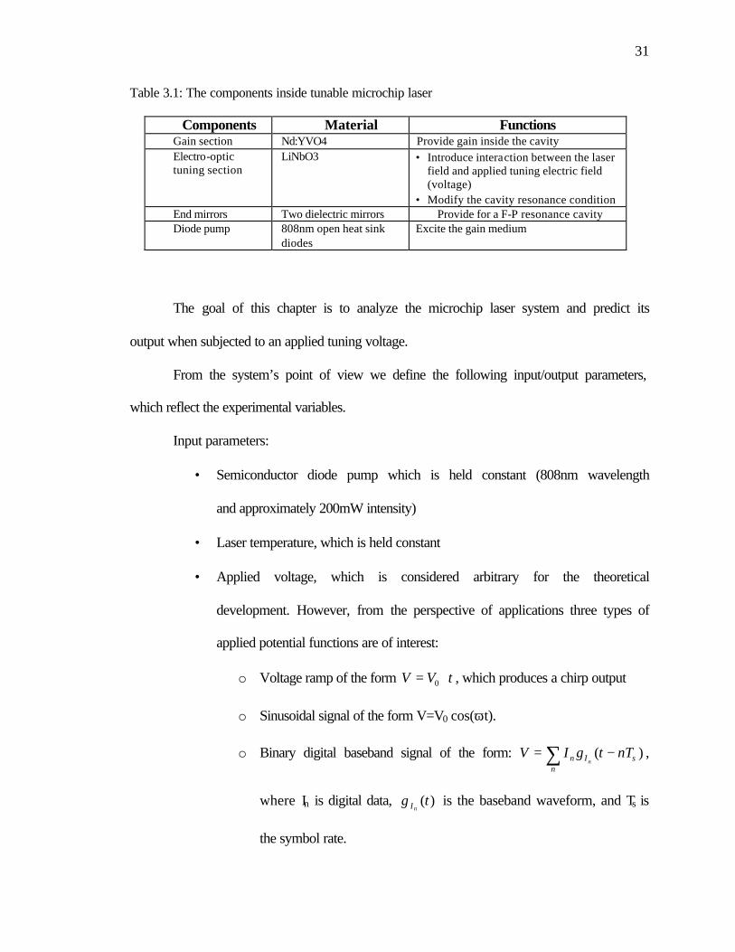
Table 3.1: The components inside tunable microchip laser
Components Material Functions Gain section Nd:YVO4 Provide gain inside the cavity Electro-optic tuning section
LiNbO3 • Introduce interaction between the laser field and applied tuning electric field (voltage)
• Modify the cavity resonance condition End mirrors Two dielectric mirrors Provide for a F-P resonance cavity Diode pump 808nm open heat sink
diodes Excite the gain medium
The goal of this chapter is to analyze the microchip laser system and predict its
output when subjected to an applied tuning voltage.
From the system’s point of view we define the following input/output parameters,
which reflect the experimental variables.
Input parameters:
• Semiconductor diode pump which is held constant (808nm wavelength
and approximately 200mW intensity)
• Laser temperature, which is held constant
• Applied voltage, which is considered arbitrary for the theoretical
development. However, from the perspective of applications three types of
applied potential functions are of interest:
o Voltage ramp of the form tVV ⋅= 0 , which produces a chirp output
o Sinusoidal signal of the form V=V0 cos(ωt).
o Binary digital baseband signal of the form: ∑ −=n
sIn nTtgIVn
)( ,
where In is digital data, )(tgnI is the baseband waveform, and Ts is
the symbol rate.
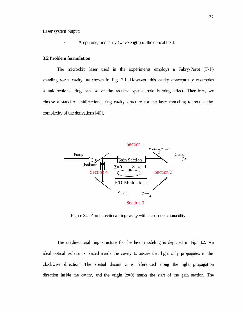
32
Laser system output:
• Amplitude, frequency (wavelength) of the optical field.
3.2 Problem formulation
The microchip laser used in the experiments employs a Fabry-Perot (F-P)
standing wave cavity, as shown in Fig. 3.1. However, this cavity conceptually resembles
a unidirectional ring because of the reduced spatial hole burning effect. Therefore, we
choose a standard unidirectional ring cavity structure for the laser modeling to reduce the
complexity of the derivations [40].
E/O Modulator
Gain Section
Z=z 2 Z=z
3
Z=0 Z=z 1 =L
Section 3
Section 4
Section 1
Section 2
Pump Output Partial reflector: R
Isolator
Figure 3.2: A unidirectional ring cavity with electro-optic tunability
The unidirectional ring structure for the laser modeling is depicted in Fig. 3.2. An
ideal optical isolator is placed inside the cavity to assure that light only propagates in the
clockwise direction. The spatial distant z is referenced along the light propagation
direction inside the cavity, and the origin (z=0) marks the start of the gain section. The
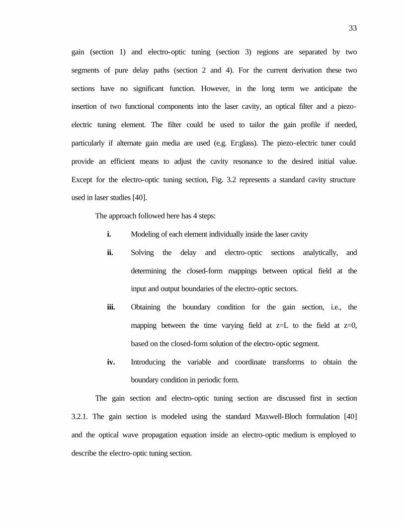
33
gain (section 1) and electro-optic tuning (section 3) regions are separated by two
segments of pure delay paths (section 2 and 4). For the current derivation these two
sections have no significant function. However, in the long term we anticipate the
insertion of two functional components into the laser cavity, an optical filter and a piezo-
electric tuning element. The filter could be used to tailor the gain profile if needed,
particularly if alternate gain media are used (e.g. Er:glass). The piezo-electric tuner could
provide an efficient means to adjust the cavity resonance to the desired initial value.
Except for the electro-optic tuning section, Fig. 3.2 represents a standard cavity structure
used in laser studies [40].
The approach followed here has 4 steps:
i. Modeling of each element individually inside the laser cavity
ii. Solving the delay and electro-optic sections analytically, and
determining the closed-form mappings between optical field at the
input and output boundaries of the electro-optic sectors.
iii. Obtaining the boundary condition for the gain section, i.e., the
mapping between the time varying field at z=L to the field at z=0,
based on the closed-form solution of the electro-optic segment.
iv. Introducing the variable and coordinate transforms to obtain the
boundary condition in periodic form.
The gain section and electro-optic tuning section are discussed first in section
3.2.1. The gain section is modeled using the standard Maxwell-Bloch formulation [40]
and the optical wave propagation equation inside an electro-optic medium is employed to
describe the electro-optic tuning section.

34
The modeling of the entire tunable laser system is performed in section 3.2.2, in
which we first derive an analytic solution of the electro-optic tuning section and then use
this result to determine the boundary conditions for the tunable laser system and obtain
the equations of motion for the entire tunable laser system.
3.2.1 Modeling of components In this section, we model the individual components of the laser. As shown in Fig.
3.2, the overall laser system is comprised of: the gain, electro-optic, and delay sections.
The delay sections introduce a constant time delay, which can be directly specified (see
Table 3.2).
In the modeling process, we do not consider the transverse profile of the lasing
mode. The space coordinate, z, in the subsequent derivations is the physical distance
multiplied by the initial index of refraction, or the effective optical length. The optical
field inside the laser cavity can be expressed in terms of a plane wave carrier and a
slowly varying field envelope
.].),([21
),( )( CCetzztE tzki cc +⋅= −⋅ ωξ
where ),( tzξ is the envelope of the optical field, Λ
⋅⋅=
cmc
πω
2is the initial cold cavity
(i.e., zero applied voltage across the electro-optic section) resonance frequency that is
closest to the atomic resonance, m is an integer, Λ is the initial optical length of the
cavity, c is the speed of light in a vacuum, and kc is the wave number, c
k cc
ω= . It should
be noted that even though the selection of the plane wave carrier frequency can be any
value near the atomic resonance, we choose the frequency for the cavity resonance to
reduce complexities in the boundary condition.

35
Next, we are going to model each element of the cavity.
i. Gain section Our analysis of the dynamic behavior inside the gain medium is based on the
Maxwell-Bloch formulation [40] for a plane wave optical field and a homogeneously
broadened two-level active medium. In order to obtain a simpler form of the equations of
motion, we employ the dimensionless field envelope, i.e., the Rabi frequency,
2/1|| )/(
2~γγ
µξ⋅=Ω ⊥h
[40], where ⊥γ and ||γ are the decay rates of driving polarization
and population inversion, respectively. The Rabi frequency will be used in the subsequent
sections as well. Under the slowly varying field envelope approximation (SVEA), the
equations of motion for the dimensionless field envelope and atomic variables have the
following form [40]:
),(),(
~),(
~ztPc
zzt
ct
zt⋅⋅=
∂Ω∂
⋅+∂
Ω∂α (3.1.a)
),(),(~
),()~
1(),(
ztdztztPit
ztPAC ⋅Ω⋅++−=
∂∂
⊥⊥ γδγ (3.1.b)
)),(),((.).),(),(~
(21),(
||*
|| ztdztdccztPztt
ztd eq−−+⋅Ω−=∂
∂γγ (3.1.c)
where P(t,z) is the dimensionless envelope of the macroscopic driving polarization, d is
the population difference per atom between the upper and lower lasing levels, µ is the
microscopic dipole moment of the laser medium, deq is the equilibrium inversion
difference per atom, α is the unsaturated gain per unit length, and ACδ~
is the normalized
detuning between the atomic resonance and the selected cavity resonance in units of ⊥γ .
Next, we’ll discuss the modeling of the electro-optic tuning section.
36
ii. The electro-optic modulation section
Usually, the electro-optic section is dealt with as a lumped element phase
modulator [32-38], where the time varying voltage introduces an optical phase change
proportional to the voltage. However, in the case where the length of the electro-optic
tuning section is comparable to the entire laser cavity length, or if the change in the
modulating waveform cannot be neglected during the transit time within the electro-optic
section, this assumption is no longer valid because the traveling wave effects may be
significant. Therefore, we employ a rigorous wave propagation model, in which the
optical field inside is described by the following wave propagation equation [43]:
),(1
),(),( /2
2
022
2
2
2
2
2
tzPtc
tzEtc
ntzE
zoe
∂∂
⋅⋅
=∂∂
−∂∂
ε (3.2)
where n is the refractive index of the electro-optic material when no voltage is applied,
E(z,t) is the optical field inside the electro-optic section, Pe/o is the driving polarization
responsible for electro-optic effect. For a z cut LiNbO3 electro-optic crystal,
)(),(330/ tEtzEdP tuningoe ⋅⋅⋅= ε (3.3)
where 33d is the nonlinear optical coefficient and tuningE is the tuning field.
The nonlinear polarization term on the right hand side of Eq. 3.2 is responsible for
the electro-optic modulation. Applying the SVEA to Eq. 3.2 and assuming the applied
tuning voltage is slow-varying compared with the oscillation of the optical field
(~1015Hz), we obtain the propagation equation for the complex envelope of the optical
field
),()(2
),(),(332
tztEdn
iz
tznc
ttz
tuningc ξ
ωξξ⋅⋅⋅⋅=
∂∂
+∂
∂ (3.4)

37
where ξ is the complex field envelope.
Since the electro-optic element is placed inside the laser cavity, it is more
convenient to employ the dimensionless field envelope Ω~ (i.e., Rabi frequency). The
result is Eq. 3.5.
),(~)(2
),(~
),(~
3320
0 tztEdn
iz
tzc
ttz
tuning Ω⋅⋅⋅⋅=∂
Ω∂+
∂Ω∂ ω
(3.5)
Recall that for the laser modeling, we use the effective optical length for the space
coordinate. Therefore, there is no explicit dependence on the refractive index on the left
hand side of Eq. 3.5.
Table 3.2 summarizes the modeling equations for the optical field envelope and
initial conditions in each sub-section of the laser cavity.
In the next section, we will derive the analytical solution of the electro-optic
section, and use it to obtain the boundary condition for the gain section and the
formulation for the dynamics of the entire tunable laser system.

38
Table 3.2: Field envelope equations, boundary and initial conditions, in each sub-sections of the laser cavity
Section id Modeling equation(s) Field continuity conditions Initial Conditions
Comments
Gain Section Maxwell-Bloch Equation for plane waves:
Pcz
ct
⋅⋅=∂Ω∂
⋅+∂Ω∂
α~~
dPitP
AC ⋅Ω⋅++−=∂∂
⊥⊥~
)~
1( γδγ
)()~~(21
||**
||eqddPP
td
−−⋅Ω+⋅Ω−=∂∂
γγ
Maxwell field: ),(),0( tzEtzE Λ=== Field
envelope:
),(~),0(~ tztz Λ=Ω==Ω
Initial steady state field:
)0,(~
−=Ω tzstead
Ω: Rabi frequency P: the driving polarization d: the inversion probability deq: the equilibrium inversion probability c: speed of light α : unsaturated field absorption coefficient
ACδ~
: Detuning between
the cavity resonance frequency and atomic resonance
⊥γ , Cγ : decay constant
Delay section (section 2)
Delay:
)/(~),(~ czttz −Ω=Ω
Maxwell field:
),(),( 11 tzzERtzzE −+ =⋅==Field envelop:
),(~),(~11 tzzRtzz −+ =Ω⋅==Ω
The initial steady state field:
)0,(~
−=Ω tzstead
R: The output mirror reflectivity.
Electro-optic section
Wave propagation equations under slowly varying envelop approximation:
Ω⋅⋅⋅⋅=∂Ω∂
+∂Ω∂ ~
)(2
~~332
0
0 tEdn
iz
ct tuning
ω
Maxwell field:
),(),( 22 tzzEtzzE −+ === Field envelope:
),(~),(~22 tzztzz −+ =Ω==Ω
The initial steady state field:
)0,(~
−=Ω tzstead
ω0: optical frequency; d33: nonlinear efficient of LN; Etuning: tuning electric field.
Delay Section (section 4)
Delay:
)/(~),(~ czttz −Ω=Ω
Maxwell field:
),(),( 33 tzzEtzzE −+ ===
Field envelope:
),(~),(~33 tzztzz −+ =Ω==Ω
The initial steady state field:
)0,(~
−=Ω tzstead
38

39
3.2.2 Overall cavity formulation The overall cavity formulation of the composite ring laser cavity requires
concatenation of the individual system blocks. From Table 3.2, we find that the equations
representing the gain section are complicated and have no closed-form solution, while the
electro-optic tuning section has a relatively simple field equation. Therefore, the
reasonable approach may be comprised of the steps outlined in the following flow chart.
Solve E/O section analytically and derive the closed form relationship between the input and output boundary of E/O section subject to the applied field and the initial condition (t=0) provided by the steady state solution
Derive the formal boundary condition for the tunable laser cavity based on the solution for the E/O section.
Introduce variable and coordinate transform to obtain the formulation equations with the normal boundary condition
The complete E/O tunable laser dynamics becomes the dynamics problem inside the
gain section
Obtain the steady state solution for the electro-optic and gain sections
E/O section
Gain section
Steady state t=<0 Etuning(t)=0
Dynamic t>0 Etuning(t)!=0
Dynamic t>0 Etuning(t)!=0
Figure 3.3: The electro-optic tunable laser formulation process

40
For the time period t=0, no external electric field is applied and the system is in
steady state, with a known solution. This steady state serves as the initial condition for
the system. At t=0, an electric field is applied, which perturbs the system. We anticipate
that the principal effect of the applied field is to induce a time dependent phase delay, or
frequency shift as the optical field propagates across the electro-optical section. In
subsection 3.2.2, we solve the electro-optic section analytically and obtain the closed-
form functional mapping from its input to its output field envelope. Later, the mapping is
employed to acquire a boundary condition for the gain medium. Up to this point, the
complicated dynamics involving the interaction between the electro-optic section and the
nonlinear gain medium becomes a more manageable problem for the gain medium.
Next, we explain this process in detail.
i. Closed-form solution of the electro-optic tuning section
The objective of this section is to solve the propagation equation inside the
electro-optic section (Eq. 3.5) with the initial condition, and the knowledge of the tuning
potential. The propagation equation is a first-order partial differential equation for which
a closed-form solution exists (Appendix A). The complex field envelope at the output
boundary of the electro-optic section is given by
)(323 ),(
~),(
~ tietzztzz Φ⋅⋅−=Ω==Ω τ (3.6)
where ∫ −=Φ
t
t tuning duuVt
3
)()(τ
β , 3320
0
2d
hn⋅
⋅=
ωβ , h is the thickness of the electro-optic
modulator, and Vtuning(t) is the applied voltage.
As shown in Eq. 3.6, the time dependent external field produces a time-varying
phase shift, ? (t), and a constant time delay, τ3. The derivative of the time dependent

41
phase leads to the frequency shift, dtdΦ
, which is responsible for frequency modulation
inside the laser cavity.
Next, we will use the closed-form solution for the electro-optic section to obtain
the boundary condition for the gain section.
ii. Boundary condition for the electro-optic tunable laser
In subsection a, we solved the mapping between the input and output complex
fields of the electro-optic tuning section. Now, we use this closed-form mapping to
concatenate the delay paths, electro-optic tuning section, and gain section to acquire a
self-consistent boundary condition for the gain section. First, we write down the optical
field at end of the gain section, z=L,
.].)/(
2),(
~[
21
),( )(
2/1| |
ccetLz
tLzE tLki cc +⋅⋅
=Ω⋅== −⋅
⊥
ω
γγµh
(3.7a)
Then, from the result for the delay section 1 in table 3.2, we find the optical field
at z=z2, is
.].)/(
2),(
~[
21
),( )(
2/1| |
22
2 ccetLz
RtzzE tzki cc +⋅⋅
−=Ω== −⋅
⊥
ω
γγµ
τ
h
(3.7b)
Employing the closed-form solution (Eq. 3.6) of the electro-optical section, we
get the expression for the optical field at z=z3,
.].)/(
2),(
~[
21
),( )()(
2/1| |
323
3 cceetLz
RtzzE tzkiti cc +⋅⋅⋅
−−=Ω⋅== −⋅Φ
⊥
ω
γγµ
ττ
h
(3.7c)
Finally, the optical field at z= Λ , can be calculated similarly using the result for
delay section 4 (Table 3.2).

42
c.c.]ee)?/(?
2µ)ttttL,(zO
~[R
21
t)? ,E(z t)??(ki)t(ti
1/2| |
432 cc4 +⋅⋅⋅
−−−=⋅== −⋅−Φ
⊥h
(3.7d)
When expressed in term of a field envelope and a carrier, the optical field at z=0 is,
.].)/(
2),0(
~[
21
),0( )0()(
2/1| |
4 cceetz
RtzE tkiti cc +⋅⋅⋅
=Ω⋅== −⋅−Φ
⊥
ωτ
γγµh
(3.7e)
Since t)? ,E(z = and ),0( tzE = describes the field at the same physical location,
the following boundary condition for the field envelope has to be satisfied,
Λ⋅⋅−−Φ⋅ ⋅⋅⋅++−=Ω==Ω ckiti eeRtLztz )(423
4))(,(~
),0(~ ττττ (3.8a)
Noted that the carrier frequency is selected to be the cavity resonance, i.e.,
Λ⋅=
π2mk c , m is an integer, the boundary condition is reduced to the following form,
)(423
4))(,(~
),0(~ ττττ −Φ⋅⋅⋅++−=Ω==Ω tieRtLztz (3.8b)
The new boundary condition, Eq. 3.8b, together with the Maxwell-Bloch
equations, Eq. 3.1, defines the complete dynamic behavior of the entire tunable laser
system. Except for the additional time dependent phase lag induced by the electro-optic
modulation, Eq. 3.8b is very similar to the boundary conditions of the lasers without
electro-optic tuning [40].
The current microchip laser system has a negligible air gap (< 2% total cavity
length). For simplicity of the discussion, we let the delay time in sections 2 and 4 vanish,
i.e., 042 == ττ . Then the boundary condition is reduced to,
)(3 ),(
~),0(
~ tieRtLztz Φ⋅⋅⋅−=Ω==Ω τ (3.9)

43
With a time delay and a time dependent phase )( tie Φ , the boundary condition
given by Eq. 3.9 is complicated. Next, we will use coordinate and variable transforms to
obtain a boundary condition in normal (periodic) form. It should be emphasized that the
technique employed to simplify the boundary condition is valid even when the air gap
exists.
To eliminate the explicit time delay, the coordinate transformation introduced by
Benza and Lugiato [44], is employed
Lzttzz
/3 ⋅+=′=′
τ (3.10)
In (t’,z’) coordinates, the boundary condition is simplified:
)(),(~
),0(~ tieRtLztz ′Φ⋅⋅⋅′=′Ω=′=′Ω (3.11)
At this stage, it is convenient to introduce a field variable transform to eliminate
the time varying phase and loss in the boundary condition:
),(ln
),(),(~ tzGizLR
eetzFtz ′′⋅′−⋅⋅′′=′′Ω
),(ln
),(),( tzGizLR
eetzptzP ′′⋅′−⋅⋅′′=′′ (3.12)
where F(z’,t’) and p(z’,t’) are the new field envelope and polarization envelope variable,
and G(z’,t’) is an unknown function that satisfies the following constraint:
)(),(),0( ttLzGtzG ′Φ+′=′=′=′ (3.13)
Then, the boundary condition for the new field variable F(z’,t’) is in the normal
form,
)','()',0'( tLzFtzF === (3.14)

44
In order to complete the definition of the new field and polarization variables, the
exact form of the function G(z’,t’) needs to be determined. However, the constraint (Eq.
3.13) is rather loose and an infinite number of candidates exist for G(z’, t’). To select the
most appropriate one, we substitute the transforms (Eq.3.12) into the Maxwell-Bloch
equations (3.1) and obtain the new equation of motion for the new field and polarization
variables as the following,
∂∂
⋅+∂∂
+⋅⋅−⋅
+⋅⋅−=⋅∂∂
⋅+∂∂
+''
)1(ln
)','(]''
)1[(zG
ctG
bFiFL
RcpctzF
zc
tb α (3.15a)
dFpt
tzGipi
ttzp
AC ⋅⋅+⋅∂
∂⋅−+−=
′∂∂
⊥⊥ γδγ'
)','()
~1(
)','( (3.15b)
)()/)(ln'2exp(.).(21)','( * eqddLRzCCpF
ttzd
−−⋅⋅−+⋅−=′∂
∂CC γγ (3.15c)
where 13 /ττ=b , and cL
=1τ is the propagation delay in the gain section.
Inspecting Eqs. 3.15, we find that the equation of motion for the tunable laser
system will have a simple form when imposing the following additional constraint for
G(z’, t’),
0''
)1(),(),(
=∂
∂⋅+
∂∂
+′′⋅′′⋅
ze
ct
eb
tzGitzGi
(3.16)
At first sight, the constraint given by Eq. 3.16 is just a mathematical convenience.
However, we will show later its physical interpretation.
Equation 3.16 yields,
)/)1(''()','( cbztYtzG +−= (3.17)
where Y(t’) is a function to be determined by the initial condition and the boundary
condition (3.13). We assume initially Y(t’) is zero so that the new field envelope variable

45
F(z’,t’) is consistent with the original field envelope )','(~ tzΩ , when there is no electro-
optic perturbation. Thus, the initial condition for Y(t’) is the following,
0)'( =tY , 0'<t (3.18)
Substituting Eq. 3.17 into the boundary condition (3.13) and employing the initial
condition (Eq. 3.18), we obtain the closed-form solution for G(z’,t’):
∑=
=
⋅−Φ=τ
τ/
0
)()','(um
m
mutzG , c
zbtu
')1('
×+−= (3.19)
where 31 τττ += is the round trip cavity delay.
Thus, we uniquely determined G(z’,t’) . At this stage, we can write down the final
equation of motion for the new field and atomic variables under the new coordinate
system (t’, z’):
)2()','('
''
FpCktzFz
ct
+⋅−=⋅
∂∂
⋅+∂∂
(3.20a)
dFptzfipit
tzpAC ⋅⋅+⋅⋅−+−=
′∂∂
⊥⊥ γδγ )','()~
1()','(
(3.20b)
)()/)(ln'2exp(.).(21)','( * eqddLRzCCpF
ttzd
−−⋅⋅−+⋅−=′∂
∂CC γγ (3.20c)
with the periodic boundary condition (Eq. 3.14),
)','()',0'( tLzFtzF ===
where b
cc
+=′
1,
LRc
kln⋅′
−= , and RL
Cln
2α
−= are the effective speed of light, cavity
decay rate constant, and normalized small single pass gain of the laser system, and
[ ]
∑=
=
−⋅−−⋅−×=∂
∂=
τ
τττβ/
03)()()
')','(
()','(um
m
muVmuVt
tzGtzf ,
czb
tu')1(
'×+
−= (3.21)

46
where V(t) is the applied tuning voltage. )','( tzf can be treated as a modulation of the
cavity resonance frequency.
The equations of motion (Eq. 3.20) together with the boundary condition (Eq.
3.14) represent the formulation of the entire composite cavity tunable laser system.
Before proceeding further, we discuss the interpretation of )','( tziGe . In the (t’,z’)
coordinate system, Eq. 3.16 represents a complex envelope propagating in a passive,
dispersionless and lossless medium with speed of c/(1+b). While in the real (t, z)
coordinates, Eq. 3.16 describes an envelope that is propagating in such a medium with a
speed of c. Therefore, )','( tziGe represents the optical field envelope inside a passive,
lossless, unidirectional ring cavity with electro-optic modulation as shown in Fig. 3.4.
E/O Modulator
Z=z2 Z=z 3
Section 3
Section 4 Section 2
Section 1
V(t) z=0
z=L
perfect reflector perfect reflector
perfect reflector perfect reflector
Figure 3.4: An ideal model of a lossless ring cavity under electro-optic modulation
Based on this interpretation, the new field variable F(z’,t’) can be treated as a
modification imposed by the gain medium on the optical field propagating in the ideal
lossless, passive cavity in Fig. 3.4. The final equations of motion (Eqs. 3.20) are similar
to the laser modeling equations obtained by previous work [40], except for the inclusion

47
of modulation term )','( tzif . The modulation term induced a perturbation on the
detuning between the cavity resonance and atomic resonance.
In section 3.4, we will simulate the behavior of the dynamically tunable laser
system using the equations derived above. But next, the model representation of the laser
would be derived based on the periodic boundary condition (Eq. 14). Meanwhile, the
single mode operation condition for the laser under intracavity frequency modulation will
be addressed.
3.2.3 Model representation and uniform field limit Based on the periodic boundary condition (3.14), F(z’,t’), p(z’,t’) and d(z’,t’) can
be expended in Fourier series [40],
∑ ⋅⋅⋅=n
nn zkitFtzF )'exp()'()','(
∑ ⋅⋅⋅=n
nn zkitPtzp )'exp()'()','(
∑ ⋅⋅⋅=n
nn zkitdtzd )'exp()'()','(
where nL
k n ⋅=π2
, n is an integer. It should be noted that the terms Fn(t’), Pn(t’), and
dn(t’) are Fourier coefficients representing the modes of the laser in (z’,t’) coordinates.
The associate orthonormal modal functions are
zikn
neL
zu ′⋅=′ 1)(
with
nmnn
L
mn uuzdL
uu ,*
0
1),( δ=⋅⋅′= ∫

48
Substituting the above equations into the equations of the motion (Eq. 3.20), we find that
the infinite set of time-dependent variables Fn(t’), Pn(t’), and dn(t’) obey the following
equations:
mmmmm FkciPCkkF
tF
⋅⋅⋅−⋅⋅⋅+−=∂
∂2
' (3.22a)
⋅⋅+⋅+++−=
∂∂
∑∑ −⊥≠
−⊥⊥
⊥n
mnnn
nmn
mACm dFP
fiP
fii
tP
γγγ
δγ0
0 )~
1('
(3.22b)
)(.).(2
1'
*m
eqmnnn
m ddCCPFLt
d−−Γ⊗+⊗
⋅−=
∂∂
− CC γγ (3.22c)
where ⊗ is the convolution operator,
∫ ′′=L eqzikeq
m dezdL
d n
0
1
∫ ′′′= ′L zikn ztfezd
Ltf n
0),(
1)'(
∫ ⋅+−
=′=Γ ′′L
n
RLzzikn LkiRR
Rdezd
Ln
0 2
2|)|ln/(2
|ln|2111
, n is an integer
Thus, we obtained the modal representation of the electro-optic tunable laser
system, which involves coupling of an infinite number of modes and an exact solution is
very difficult to obtain. In reality, the tunable laser operates as a single mode device,
which leads to the expectation that the 0th order mode (n=0) dominates. If this is true, the
single mode approximation, or the uniform field limit in the (t’,z’) coordinate system, can
be employed to simplify the simulation.
By inspecting the model representation (Eq. 3.22), we find that the single mode
approximation is valid if no modal coupling exists. That is the following approximate
condition should be satisfied,
49
0,nn δΓ≈Γ (3.23a)
1)'(
0 <<− ⊥
≠
γnn tf
(3.23b)
The first approximation (Eq. 3.23a) repeats the previous result obtained by
Narducci et al. [40]. In order to satisfy the Eq. 3.23a, we must have:
)1(/ln0
1
OLRL
R
→→
→
αα (3.24)
The single mode requirement specifically for the laser under electro-optic tuning
is given by Eq. 3.23b, which indicates that the electro-optic perturbation only introduces
a negligible coupling between the different Fourier modes of the medium polarization.
By Eq. 3.21, the coefficient )'(tf n is calculated,
∫⋅= t'
t'-03
)()'(ττ
βduuVtf (3.25a)
[ ]∫ ∞
⋅−⋅−−⋅= t'
- 3 )()()'( dueuVuVtf uin
nωττβ
(3.25b)
where τ
πω
2⋅=
nn .
As shown in Eq. 3.25, the requirement for single mode operation relies on the
“history”, or the entire waveform of the applied tuning voltage. Next, we would discuss
briefly the single mode operation condition for different perturbation signals, namely, the
linear ramp, and periodic signal.
i. The linear ramp
If the tuning potential is a linear ramp, i.e., ttV ⋅= α)( , for t>τ3, Eq. 3.25 yields,

50
)2/'()'( 330 ταττβ
+⋅⋅⋅= ttf
23
'
3
/)1()'(
3
n
itin
n
nn eeitf
ω
τωτα
τβ τωω
−
−+⋅−⋅⋅⋅=
⋅−−
for 0≠n
where α is the voltage ramping rate. In order to satisfy the requirement for the uniform
field limit under electro-optic perturbation (Eq. 3.24b), we must have,
⋅
−⋅−
>>⋅⋅⋅−
⊥τω
ττωβατ
γτω
23
3
/)1(,
1max
1 3
n
j
n
ne for 0≠n (3. 26)
In practice, the medium gain linewidth ( ⊥γ ) of solid-state lasers are much bigger
than the frequency modulation during a round trip period (3
βατ ). Therefore, Eq. 3.26 is
always satisfied for the perturbation under linear voltage ramp.
ii. The periodic perturbation signal
When the perturbation is periodic, the situation becomes more complicated. Since
any periodic signal can be treated as a Fourier series, we only study the sinusoidal signal,
i.e.,
..21
)( )( CCAetV ti c += +δωω
where A is the amplitude, τπ
ω2
⋅= nc is the nth cavity resonance frequency, and δω is
the detuning between the frequency of the perturbation signal and cavity resonance.
Using Eq. 3.25, for t>τ3, we get
)1()2(1
2)1(
12
)( 33 )(')2(
)('
τδωωωδω
τδωωδω
ωδωτβ
δωτβ ⋅+
⋅−⋅⋅+
⋅⋅
−⋅−⋅
−⋅+−⋅
⋅−
⋅= n
n
n i
n
tii
ti
n eie
Aei
eAtf for 0≠n
In order to satisfy the requirement for single mode operation (Eq. 3.23b), we should have,

51
)1(1
23τω
γτβ
δω ⋅
⊥
−⋅>> nieA (3.27)
If the entire cavity is uniformly filled with electro-optic medium, i.e., ττ =3 , the single
mode condition (Eq. 3.27) always holds. Otherwise, as the detuning is reduced to zero,
the constraint given by Eq. 3.27 cannot be satisfied. The uniform field limit, or the single
mode approximation is no longer valid. The laser then operates in distorted FM
oscillation or even FM mode locking region [33].
Under the single mode approximation, the equations of motion in modal form
(Eq. 3.22) are reduced to the form of simple O.D.E.,
000 2
')'(
PCkkFt
tF⋅⋅⋅+−=
∂∂
(3.28a)
)()()~
1('
)'(00000
0 tPtfidFPittP
AC ⋅+⋅⋅++−=∂
∂⊥⊥ γδγ (3.28b)
)(.).(21
')'(
0*
000 eqddCCPFttd
−−+⋅−=∂
∂CC γγ (3.28c)
Comparing Eq. 3.28 with the equations of motion in the uniform field limit for
lasers without electro-optic tuning, we find that the electro-optic tuning simply introduces
a time-dependent perturbation to the cavity resonance frequency, namely, )(0 tf .
However, the cavity resonance frequency tuning is not a simple function of the tuning
potential. Instead, it assumes an integral form (averaged over a time period 3τ ). This is
the result of the distributed modeling of the electro-optic tuning section. When the tuning
voltage is kept constant, the cavity resonance frequency tuning is reduced to the
conventional form, that is. ττβ /)( 30 Vtf ⋅= .

52
Next, we will derive an approximate, closed-form solution for the tunable laser
with the assumption that the frequency tuning is small compared with the gain linewidth.

53
3.3 Linear dynamics model
From section 3.2, we show that the solution inside a conceptual lossless cavity
can be treated as the 0th-order approximation of the laser field by neglecting the
frequency pulling effect of the gain medium. The new field variable F(z’,t’) provides the
correction to this estimation. As shown in Eq. 3.21, because the electro-optic section does
not occupy the entire laser cavity, a periodic and persistent oscillation in the 0th order
estimation of the optical frequency, f(z’,t’) will occur even after the tuning voltage
reaches a steady value. This raised the concern whether or not this oscillation is a
transient effect for the real optical field and its decay time. In this section, we provide the
answer to this problem analytically.
The Maxwell-Bloch equations are complicated and the exact closed-form solution
is impossible to obtain. However, in many cases of interest for microchip lasers system,
the modulation to the cavity resonance frequency )','( tzf is much smaller than the gain
linewidth ( ⊥γ ). Thus, we can linearize the dynamic system in the proximity of the initial
steady state (see section 3.3.1); then we will seek an approximate analytical solution in
the frequency domain (section 3.3.2) to prove analytically that the frequency ripple effect
is transient; finally we calculate the time constants that govern the transient behavior as
the laser frequency reaches the steady state (section 3.3.3). The objective is to identify the
new steady state value of optical frequency after the electro-optic perturbation and find
out how long it takes to reach this value.

54
3.3.1 Linearized Maxwell-Bloch equations When the optical field is experiencing a frequency offset from the initial state, a
significant amount of deviation of its field envelope from the initial value will occur.
Therefore, it is improper to use perturbation method directly for the field envelope.
Instead, we employ the perturbation technique for the modulus of the field envelope and
the relative phase. First, we express the envelopes of the field F(z’,t’), and polarization,
p(z’,t’), in terms of a modulus and a phase
)','()','()','( tziF
FetzAtzF φ⋅⋅=
)','()','()','( tziP
PetzAtzp φ⋅⋅= (3.29)
Substituting Eq. 3.29 into Eq. 3.20, we get:
)cos2()','()'
'( FpF AACktzAz
ct
+⋅−=∂∂
+′∂
∂θ (3.30a)
θφ sin2)','()'
'(F
pF A
ACktz
zc
t⋅⋅−=
∂∂
+′∂
∂ (3.30b)
θγγ cos'
⋅⋅+−=∂∂
⊥⊥ dAAAt FPp (3.30c)
θγδγθφ sin))','(~~
()('
⋅⋅
−+−=+∂∂
⊥⊥P
FACF A
dAtzf
t (3.30d)
)(cos'
/ln2 eqII
LRzPFII ddeAAd
t−−⋅−=
∂∂ − γθγ (3.30e)
where Fp φφθ −= is the relative phase between the medium polarization P(z’,t’) and the
field variable F(z’,t’), and )','(1~
tzff⊥
=γ
is the normalized effective perturbation.
The dynamic system is in steady state before the voltage is applied. Then, after
the electro-optic tuning, the field and atomic variables become:

55
FstFF AAA δ+= (3.31a)
PstPP AAA δ+= (3.31b)
ddd st δ+= (3.31c)
δθθθ += st (3.31d)
FstFF δφφφ += (3.31e)
where the subscript “st” indicates steady state value.
Based on the assumption that the electro-optic perturbation is much less than the
medium gain bandwidth, ⊥⊥ << γγ )','(~
tzf , we assume FAδ , PAδ , dδ , and 1<<δθ . It
should be emphasized that no assumption is made regarding the phase change, Fδφ ,
which is not necessarily small. Substituting Eq. 3.31 into Eq. 3.30, we get the linearized
equations of motion for the terms FAδ , PAδ , dδ , δθ and Fδφ :
δθθδθδδ ⋅⋅⋅+⋅⋅⋅−−=∂∂
+′∂
∂ ststPP
stFF ACkACkAkA
zc
tsin2cos2)
''( (3.32a)
δθθ
δθδθδφ
ststF
stP
Pst
stF
Fst
stF
stP
F
AA
Ck
AA
CkAAA
Ckz
ct
cos2
sin1
2sin)(
2)'
'( 2
⋅⋅−
⋅⋅−⋅⋅=∂∂
+′∂
∂
(3.32b)
δθθγδθγδγδ stststFF
ststPp dAAdAA
tsincos
'⋅⋅−⋅⋅+−=
∂∂
⊥⊥⊥ (3.32c)
δθθγδθγ
δθγδθγγδθδφ
⋅⋅⋅
−⋅⋅−
⋅⋅
+⋅⋅−−=+∂∂
⊥⊥
⊥⊥⊥
ststP
ststFst
stP
stF
Pst
stP
ststF
Fst
stP
st
F
A
dAd
AA
AA
dAA
A
dtzf
t
cossin
sin)(
sin)','(~
)(' 2
(3.32d)
56
deAA
AeAAeAdt
IILRzstst
PstFII
PLRzstst
FIIFLRzstst
PII
δγδθθγ
δθγδθγδ
−⋅+
⋅⋅−⋅−=∂∂
−
−−
/ln2
/ln2/ln2
sin
coscos' (3.32e)
Substituting Eq. 2.29 into Eq. 3.14, we obtain the boundary condition for AF and φF,
),'(),0'( tLzAtzA FF === (3.32f)
πφφ 2),'(),0'( ⋅+=== ntLztz FF (3.32g)
For simplicity, we assume that initially, the cavity resonance and atomic resonance
overlap, and the laser is in the uniform field limit, which is valid for a high Q laser cavity.
Under this situation, the steady state field, polarization, and inversion density can be
evaluated as:
0
2/1
2/1
1
=
=
=
=
st
st
stP
stF
Cd
CA
A
θ
(3.33)
where kcC /'2 α= .
Then, Eq. 3.32 becomes,
PFF ACkAkAz
ct
δδδ ⋅⋅−−=∂∂
+′∂
∂2)
''( (3.34a)
Fst
Pp AdAAt
δγδγδ ⋅+−=∂∂
⊥⊥' (3.34b)
dAAAAdt IIP
stFIIF
stPII δγδγδγδ −⋅−−=
∂∂
' (3.34c)
δθδφ kz
ct F =
∂∂
+′∂
∂)'
'( (3.34d)

57
δθγγδθδφ ⋅−−=+∂∂
⊥⊥ )','(~
)('
tzft F (3.34e)
Eqs. 3.34a~c and Eqs. 3.34d~e are two independent sets of equations. The first set
is self-consistent and homogeneous. Thus, if stable, they will rest in the steady state.
Therefore, the first order effect of electro-optic modulation would not change the
modulus of the field, polarization, and inversion density. The frequency/phase
information is determined by Eqs. 3.34d~e with the boundary condition. Equations
3.34d~e can be rewritten as:
δθδω'
)'
'(t
kz
ct F ∂
∂=
∂∂
+′∂
∂ (3.35a)
δθγγδθδω ⋅−−=∂∂
+ ⊥⊥ )','(~
'tzf
tF (3.35b)
where Fδω is the instant frequency change of the new field variable, FF tδφδω
'∂∂
= . It
satisfies the boundary condition:
),'(),0'( tLztz FF === δωδω (3.35c)
Thus, we have obtained the linearized equations describing the evolution of
optical frequency as a function of the applied voltage. Next, we derive its closed-form
solution in the frequency domain.
3.3.2 Closed-form solution in frequency domain It is convenient to study the equations for the optical frequency (Eq. 3.35) in the
frequency domain where Eq. 3.35 has a simpler form as shown below,
δθωδωω ⋅⋅=∂∂
+ ikz
ci F)'
'( (3.36a)
δθγωγδθωδω ⋅−−=⋅+ ⊥⊥ ),'(~ zFiF (3.36b)

58
where ),'(~ ωzF is the Fourier transform of ),'(~
tzf .
The corresponding boundary condition in the frequency domain is
),'(),0'( ωδωωδω Lzz FF === (3.36c)
Combining Eqs. 3.36a and 3.36b we get,
ωγωγ
ωωδωωδωωγ
ωizF
ikzz
czi
ki FF +
⋅⋅⋅−=
∂∂
⋅+⋅+
+⋅⊥
⊥
⊥
),'(~
),'('
'),'()1( (3.37)
With the boundary condition, Eq. 3.37 yields the following closed-form solution:
),0'(~
1
1),0'(
)1(ωγωδω
ωγτω
ωγτω
=
−
−−==
++⋅
+⋅
⊥
⊥
⊥
zF
e
ez
ik
i
ik
i
F (3.38)
where τ is the cavity round trip delay. Note that the real envelope of the optical field is
given by (see Eq. 3.12):
),(ln
),(),( tzGizLR
eetzFtz ′′⋅′−⋅⋅′′=′′Ω .
Therefore, the tuning in the instantaneous optical frequency is:
),0(~
1
11),0'(),0(
)1(ωγωδωωδω
ωγτω
ωγτω
=⋅
−
−−====
++⋅
+⋅
⊥
⊥
⊥
zF
e
ezz
ik
i
ik
i
(3.39)
where the coordinate transformation 3.10 is employed to change Eq.39 back to the (z, t)
space.
Thus, we obtained the final result of this derivation, which gives the instantaneous
optical frequency as a function of ),0(~ ω=zF . The dynamics of the entire tunable laser
reduces to a linear system, as is depicted in Fig. 3.5. In this simplified approach, the gain
medium act as a linear filter H(? ), which filters the error produced by the 0th-order

59
estimation of the optical frequency. A sample of the transfer function, H(ω), is plotted
against the normalized frequency in Fig. 3.6, where the cavity round trip time is equal to
1/ ⊥γ and the frequency and time parameters are normalized with respect to ⊥γ .
Figure 3.5: Transformation characteristics of the gain medium
Figure 3.6: The transfer function of laser dynamic system.

60
Referring to Fig. 3.6, we mote that close to zero frequency the transfer function
H(? ) is slightly below unity, which represents the precise shift of the cavity resonant
frequency. This means that the change in the instantaneous optical frequency is slightly
smaller than the change in the cavity resonance. The behavior is attributed to the well-
known mode pulling effect[45].
More importantly, the transfer function is zero at the cavity FSR or its multiples.
This suggests that the oscillation existing in the 0th order estimation (i.e., f(t’z’)) can only
be a transient effect. The gain medium will eventually smooth out these oscillations.
Next, we derive a closed-form estimation for the decay time constant of the
frequency ripples, namely the time for the instantaneous frequency to reach the steady
state.
3.3.3 The transient characteristics of the laser response with frequency tuning In this section, we study the transient characteristics of the laser frequency as it
reaches the new steady state. The discussion here is in real (t, z) coordinates. Examining
Eq. 3.21, we find that after the electro-optic tuning, the effective electro-optical
perturbation ),( ztf is a periodic function with a period equal to the cavity round trip
time. In the transient period, therefore, )0,( =ztf can be expanded using the Fourier
series,
∑ ⋅⋅==>n
tin
nefztf ω)0,0( (3.40)
where FSRnn ⋅⋅= πω 2 , and it is assumed here that the tuning voltage remains constant
after t=0.

61
The Fourier component tin
nef ω⋅ can be considered as an independent exciting
source for the linear system, H(? ). Then, we expand the laser frequency turning,
),0( tz =δω , in terms of a Fourier series with a slow time-varying Fourier coefficient.
∑ ⋅⋅⋅==n
tin
nettz ωδωδω )(),0( (3.41)
If the change of )(tnδω is negligible during the cavity round trip time, each
spectral component tj net ωδω ⋅)( does not interfere. Thus, )(tnδω can be determined from
the local characteristics of the transfer function (Eq. 3.39) in the vicinity of nω . Thus, for
any n, we can solve )(tnδω using,
)()()( 1 ωδω nnn Htuft −ℑ⊗⋅≈ (3.42)
where u(t) is a unit step function, )( nnH ωω − is an approximation of the original transfer
function )(ωH near nω , i.e.,
nHH nn ωω
ωωω→
≈− )()(
Next, we derive )(ωnH and using Eq. 3.42 to obtain the slowly varying Fourier
coefficient, )(tnδω during the transient period. To simplify the discussion, we assume the
cavity decay rate, k, is much less than the gain linewidth, which is valid for the lasers in
consideration ( k~1GHz, GHz300~⊥γ ).
i. Time evolution of the DC Fourier component
Close to DC, the transfer function H(? ) can be approximated using,
kik
e
eHi
ki
ik
i
++−≈
−
−−=⊥
→+
+⋅
+⋅
⊥
⊥
⊥
ωγγω
ωωγ
τω
ωγτω
1)
1
11()(
0
)1(0 (3.43)

62
The impulse response of the approximating system is,
tkektth ×+− ⊥⋅−= )(0 )()( γδ (3.44)
Then the Fourier component, )(0 tδω should satisfy,
−
+−⋅=⊗⋅= ⋅+−
⊥⊥⊥
⊥ )1(1~
)()(~
)( )(0000
tkek
kfthtuft γ
γγγδω (3.45)
As shown in Eq. 3.45, the DC component decays exponentially to a new steady state
value )1(~
0⊥
⊥ +−⋅
γγ
kk
f , with a time constant ⊥⊥
≈+ γγ
11k
. The steady state value is
exactly the same as the result from the mode pulling formula obtained in the steady state.
ii. The time evolution of the non-DC Fourier components
Close to the non-zero multiples of the cavity FSR, the transfer function H(? ) can
be approximated as,
)/()
1
11()(
)1( nniki
iki
n ikiii
e
eH
n
ωγωδωδωγ
γδω
ωωωγ
τω
ωγτω
++⋅
≈
−
−−=
⊥
⊥
→+
+⋅
+⋅
⊥
⊥
⊥
(3.46)
whereδω is the offset from nω , nωωδω −=
Therefore, the nth slowly-varying Fourier coefficient should satisfy,
)()(~
)( thtuft nnn ⊗⋅= ⊥γδω (3.47)
where )(thn is the impulse response of Hn(d? ). Using Fourier analysis, we get,
tktki
nnn
nn
n
n
n
n
eefikii
ft
⋅⋅+
−⋅⋅
+
⋅−
⊥⊥
⊥− ⊥⊥
⊥
⋅⋅⋅=
++
⋅ℑ=
22
2
22~)/(
~)( 1 ωγ
ω
ωγ
ωγ
γωγωδω
γδω
(3.48)

63
It is shown in Eq. 3.48 that the nth Fourier coefficient experiences ringing, and
eventually decays to zero. Both the decay rate and oscillation frequency are mode-
dependent (if we treat the Fourier components as modes), and are given by
kn
n ⋅+⊥
22
2
ωγ
ωand k
n
n ⋅+
⋅
⊥
⊥22 ωγ
ωγ, respectively. Higher order modes have a faster decay
rate. Since the optical frequency ripples vanish as the non-DC Fourier components
)(tnδω decay to zero, the decay rate of the frequency ripples should be the slowest decay
rate of the entire Fourier coefficients, which is the decay rate of the first order Fourier
mode )(1 tδω , i.e.,
( )k
FSR
FSRripple
⋅⋅+
⋅=
⊥22
2
)2(
2
πγ
πγ
(3.49)
If the laser cavity is very small, i.e., ( ) ⊥>>⋅ γπ FSR2 , the frequency ripple decay rate is
close to the laser cavity decay rate, k.
iii. Discussion
Using the approximate closed-form solution (Eq. 3.39) of the laser dynamics, we
obtained the decay rate for the 0th and higher order Fourier component induced by the
electro-optical perturbation. The 0th order component will converge to a non trivial value
given by the mode pulling formula. Therefore, it should be regarded as the ‘signal’
induced by the electro-optical perturbation. The speed of the response is given by Eq.
3.44, i.e., ⊥γ , which is very fast for microchip lasers (>200GHz).
The higher-order Fourier components vanish as the laser attains the steady state.
However, it is a slow process compared with the output ‘signal’. Therefore, they should
be best treated as an effective “noise” source. Using the result for section 3.2, we can

64
approximate the noise level, which is a function of the cavity round trip time, relative
length of electro-optic section, and the rate of ramp potential.
Next, we discuss the simulation results.
3.4 Direct simulation and discussion
In this section, the laser dynamic system (Eq. 3.28) is solved numerically by
direct integration. The objective is to analyze the transient behavior of the laser when
subjected to external force (applied potential). We use a 2nd-order two-dimensional
Runge-Kutta method for the numerically solution. A brief flow chart of the simulation
program is illustrated in Fig. 3.7. The detailed explanation of this algorithm is attached in
Appendix B.
Start
Initial condition: Fm, n=0 Pm, n=0 dm, n=0
Calculate the field, polarization, and inversion density values of the next time step (F,P,d)m>0,n+1 from the previous value (F,P,d)m,n using 2nd order R-K estimation
Enough time duration
End
n=n+1
No
Calculate the field, polarization, and inversion density at the boundary: (F,P,d)m=0,n+1 , from the boundary condition
Note: • m represents the discrete
space coordinate • n represents the discrete
time coordinate
Figure 3.7: The flow diagram for simulation

65
In section 3.1 we indicated that three types of applied signals are on interest:
linear ramp (chirp), sinusoidal, and digital. We will focus on the laser response under
linear ramp perturbation because that describes best the laser transient dynamics. The
simulations are carried out for different laser parameters and ramp rate, and the results
are summarized in this section.
3.4.1 Dynamic response of the laser In this section we examine the dynamic response of the laser system for different
applied ramp voltages. The pertinent laser parameters are summarized in Table 3.3 and,
in general, these values correspond to the attributes of the lasers used in the experiments.
However, the upper level lifetime is chosen to be 4 orders of magnitude smaller in order
to make the numeric solution less stiff [46]. One disadvantage of this change is that it
increases the speed of the amplitude response compared with the real laser.
Table 3.3: Pertinent laser parameters for the simulation
Parameters Value
Log(R): cavity loss 0.02
2C: normalized single pass gain 1.1
⊥γ : gain linewidth 200GHz
||γ : decay rate of the inversion density 1e+8
β: electro-optic modulator sensitivity 20MHz/Volt
Effective total cavity length 4.2 mm
electro-optic 80% cavity length

66
For these simulations, the speed (rate of change) and magnitude of the applied
ramp signal are varied. The speed ranges from “slow” (comparable to the current
experimental value, slew rate < 1V/ns), to “moderate” (faster, but achievable using
standard electronics, slew rate < 20V/ns), to “fast”(requires special high-speed
electronics, slew rate > 100V/ns), where the frequency tuning per round trip is not
negligible compared with the cavity FSR.
i. Laser response for slowly changing ramp voltage
The time dependence of the applied potential, the driving force, is shown in Fig.
3.8 a. There is no electric field for t<0. From t=0 to t=.05 µsec the linear ramp is applied
to the electro-optic section of the laser. For t>.05 µsec the potential is held constant at
40V.
(a) The applied voltage signal
Figure 3.8: The laser response under a ramp signal comparable to the experimental value

67
(b) Laser frequency and amplitude vs. time. No frequency ripples is clearly identified during the transient time.
Figure 3.8 (continued)
The response of the laser to this slow ramp perturbation is depicted in Fig.3.8 b.
For t<0 the laser is in steady state equilibrium. From t=0 to t=.05 µsec the optical
frequency varies linearly with the applied potential yielding a total frequency shift of .64
GHz. The slope of the frequency variation, 16 MHz/V, is the sensitivity of the electro-
optic region. The frequency shift is remarkably linear and instantaneous, just like the
experimental results presented in the next chapter. For t>.05 µsec the laser frequency
remains constant indicating that a new steady state has been reached.
The amplitude variation of the laser, also shown in Fig. 3.8 b, is slightly more
complex. After the potential is applied, a short period of ringing behavior (relaxation) is

68
observed. Approximately 1 µsec later, steady state is reached, with a slight (<0.01%)
decrease in the laser amplitude. This decrease is due to the fact that the gain profile is not
completely flat. Initially the lasing occurs at the center of the gain profile with maximum
gain. As the frequency shifts away from the center the gain slightly decreases. This is
illustrated graphically in Fig. 3.9. The amplitude relaxation oscillation is a well-
understood behavior for solid-state lasers [45].
Gai
n pr
ofile
Optical frequency
Initial Optical frequency Optical frequency
after tuning
Figure 3.9: The lasing frequency and gain profile
ii. Laser response under “moderate ramp speed”
It is instructive to investigate the laser dynamics as the ramp speed, namely the
speed of the external perturbation is increased. The laser response under a moderate
speed ramp signal, e.g. 40volt 5ns ramp signal is shown in Fig. 3.10. The frequency
variation of the laser follows the modulation signal instantly, just as before. The optical
field amplitude slowly reaches a new steady state after a period of ringing. The total
optical field amplitude variation is negligible (less than 0.1%).

69
(a) The applied voltage signal
(b) Laser frequency and amplitude vs. time
Figure 3.10: The laser response under “moderate speed”, low voltage ramp signal
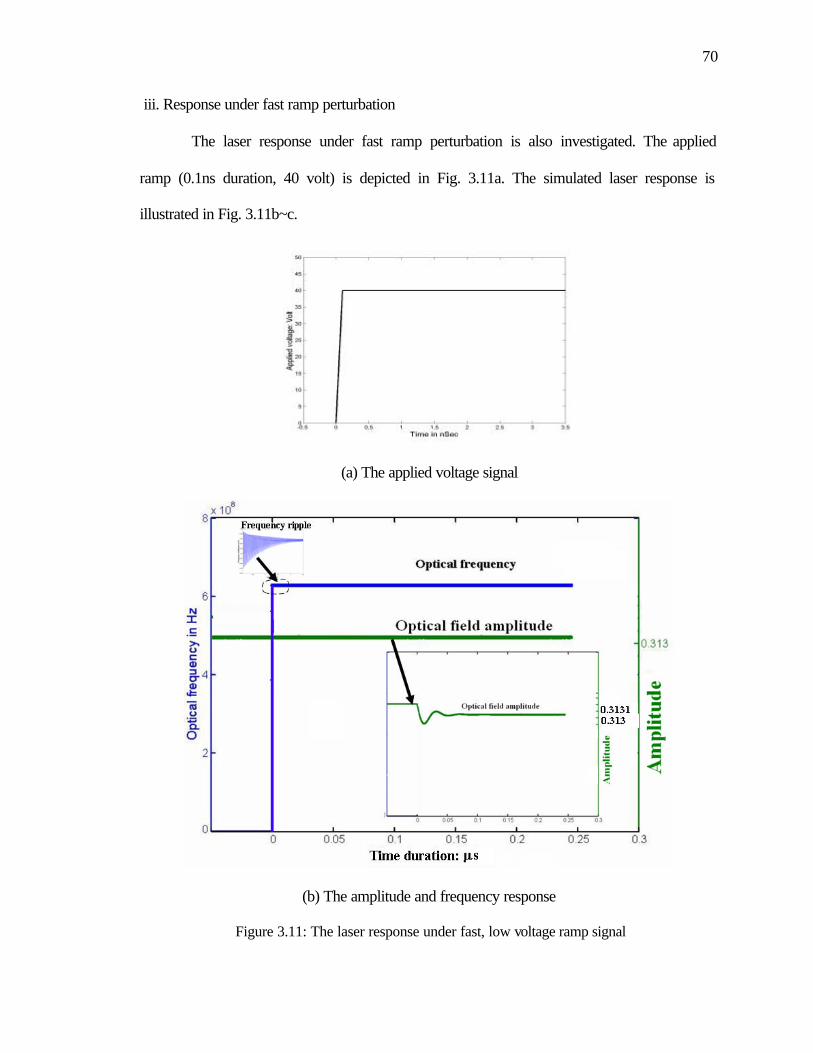
70
iii. Response under fast ramp perturbation
The laser response under fast ramp perturbation is also investigated. The applied
ramp (0.1ns duration, 40 volt) is depicted in Fig. 3.11a. The simulated laser response is
illustrated in Fig. 3.11b~c.
(a) The applied voltage signal
(b) The amplitude and frequency response
Figure 3.11: The laser response under fast, low voltage ramp signal
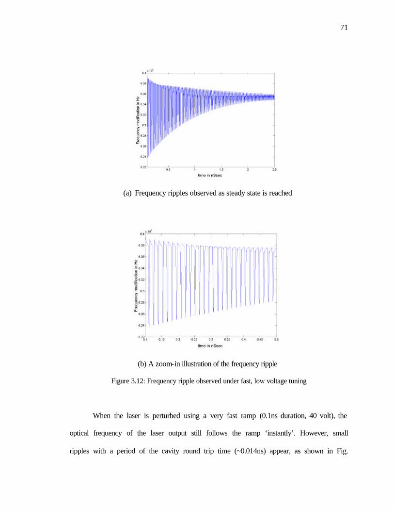
71
(a) Frequency ripples observed as steady state is reached
(b) A zoom-in illustration of the frequency ripple
Figure 3.12: Frequency ripple observed under fast, low voltage tuning
When the laser is perturbed using a very fast ramp (0.1ns duration, 40 volt), the
optical frequency of the laser output still follows the ramp ‘instantly’. However, small
ripples with a period of the cavity round trip time (~0.014ns) appear, as shown in Fig.

72
3.12. The maximum value for the ripple is less than 2% of the frequency shift between
the two steady states. The frequency ripple is attributed the fact that the electro-optic
material does not fill the entire cavity. The frequency ripples rapidly decay and vanish in
about a time period that corresponds to 180 cavity round trips. In addition, the optical
field amplitude experienced a slight variation of less than 0.1%.
iv. Response with high voltage, moderate speed ramp perturbation
It is also informative to investigate the laser response for various magnitudes of
the external voltage. A 400volt, 50ns ramp potential (Fig. 3.13a) is selected for this
purpose. The simulation results are illustrated in Fig. 3.13b~c.
(a) The applied high voltage, moderate speed tuning signal
Figure 3.13: The laser response under high voltage moderate speed ramp
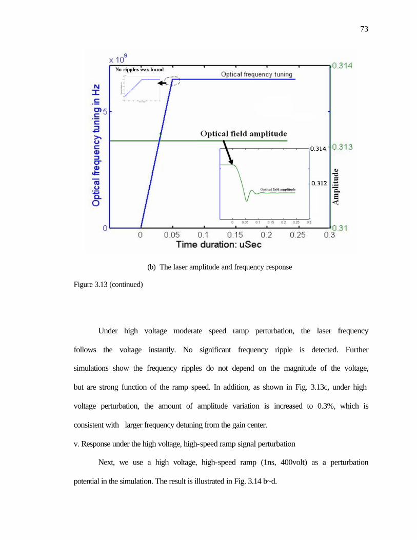
73
(b) The laser amplitude and frequency response
Figure 3.13 (continued)
Under high voltage moderate speed ramp perturbation, the laser frequency
follows the voltage instantly. No significant frequency ripple is detected. Further
simulations show the frequency ripples do not depend on the magnitude of the voltage,
but are strong function of the ramp speed. In addition, as shown in Fig. 3.13c, under high
voltage perturbation, the amount of amplitude variation is increased to 0.3%, which is
consistent with larger frequency detuning from the gain center.
v. Response under the high voltage, high-speed ramp signal perturbation
Next, we use a high voltage, high-speed ramp (1ns, 400volt) as a perturbation
potential in the simulation. The result is illustrated in Fig. 3.14 b~d.

74
(a) The applied voltage signal
(b) Laser amplitude and frequency response
Figure 3.14: The laser response under “very fast” ramp signal with high voltage

75
(c) The observed frequency ripple during the transient period
Figure 3.14 (continued)
When the laser is under the fast and high voltage ramp (1ns duration, 400volt
max), the laser frequency still follows the voltage signal almost instantaneously (Fig.
3.14b), except that optical frequency ripple occurs as before (Fig. 3.13c). The ripple
disappears after 2ns. The ripple behavior is consistent with pervious theoretical results
(section 3.2). Also shown in Fig. 3.14b, there is a “slow” amplitude variation of about
0.3%.
3.4.2 Laser dynamic behavior for different cavity parameters In this subsection, we study the laser dynamics (mode pulling, frequency ripples,
etc) vs. different cavity parameters. For these studies the speed of the driving force, the
slope of the applied ramp potential, is held constant (300Volt/ns, ~1ns duration).

76
i. The impact of the electro-optic section length
The laser’s dynamic behavior depends on the relative length of electro-optic
section. Ideally, if the entire cavity is homogenously electro-optic, the FM response is
expected to be very smooth with no observable frequency ripples. The laser parameters
used in the simulation are selected to maximize the frequency pulling effect. They are
shown in table below. The results are depicted in Figs. 3.15 ~3.18. The variation of the
optical frequency for three different electro-optic lengths is illustrated in Fig. 3.15. The
steady state tuning sensitivity as a function of the ratio between the lengths of the electro-
optic section and the entire laser cavity is plotted in Fig. 3.16. The ripple level and ripple
decay time (1/e) are depicted in Fig. 3.17 and 3.18 respectively.
Table 3.4: Laser parameters for electro-optic section length simulation
Parameters Value
Log(R): cavity loss 0.2
2C: Normalized single pass gain 1.5
⊥γ : Gain linewidth 10GHz
||γ : 1 / Upper level life time 1e+8
β: electro-optic modulator sensitivity 10MHz/Volt
L: total cavity length 67 mm

77
(a) The laser FM response when electro-optic section is 19% total cavity length
(b) The laser FM response when electro-optic section is 81% total cavity length
Figure 3.15: The laser FM response vs. different electro-optic section length

78
(c) The laser FM response when electro-optic section is 94% total cavity length
Figure 3.15 (continued)
The instantaneous frequency of the laser experiences very large oscillation with
short electro-optic section (e.g. 20% the length of the cavity). In addition, for this case the
frequency shift is small (.52 GHz). In contrast as long as the electro-optic section of the
laser is comparable to the cavity length (80% or higher) the laser approaches steady state
rather quickly, and with very little ‘oscillations’ (see Figs 3.15 b and c.). And for these
cases the frequency shift is larger. In addition, the mode pulling effect [45] is observed as
the laser reaches the steady state, but it is independent of the relative length of the
electro-optic section.
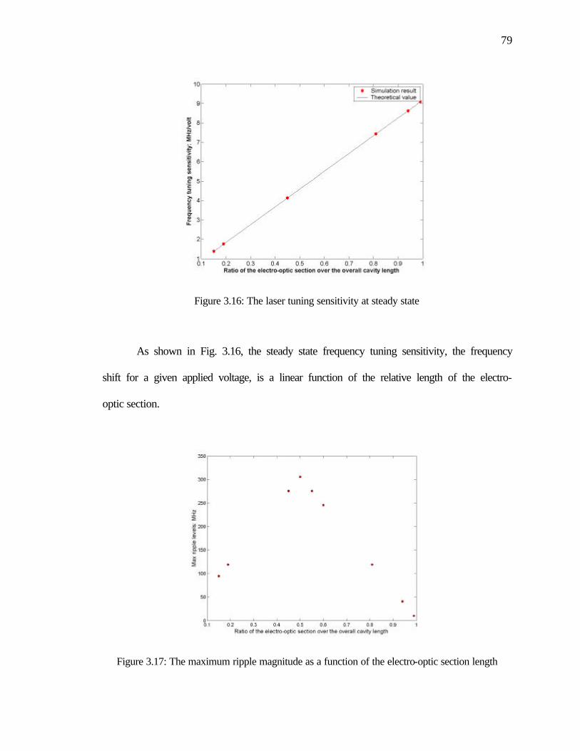
79
Figure 3.16: The laser tuning sensitivity at steady state
As shown in Fig. 3.16, the steady state frequency tuning sensitivity, the frequency
shift for a given applied voltage, is a linear function of the relative length of the electro-
optic section.
Figure 3.17: The maximum ripple magnitude as a function of the electro-optic section length

80
Figure 3.18: The ripple decay time as a function of the electro-optic section length
The simulated characteristics of the frequency ripple are displayed in Figs. 3.17,
and 3.18. The ripple amplitude is a triangular function of the relative electro-optic section
length, with maximum ripple occurring when the electro-optic section is half of the cavity
length. The simulations suggest that the ripple decay time is unrelated to the relative
length of the electro-section, which agrees with the theoretical predication (see Eq 3.49).
The predicated decay time is less than the simulated value by 30% and this is caused by
the error in measuring the decay time from the simulated time response.
Next, we will study the effect of the gain linewidth on the laser FM response.
ii. Effect of gain linewidth ⊥γ on the laser dynamics
The laser response is simulated for different gain medium linewidths. The laser
parameters for this simulation are selected to maximize the ripple and frequency pulling
effect. They are listed in table 3.5.

81
Table 3.5: Common parameters for gain linewidth simulation
Parameters Value
Log(R): cavity loss 0.2
2C: Normalized single pass gain 1.5
||γ: 1 / Upper level life time
1e+8
β: electro-optic modulator
sensitivity
10MHz/Volt
L: total cavity length 67 mm
electro-optic section length 54 mm
(a) Gain Linewidth: ⊥γ =25GHz
Figure 3.19: The laser FM response vs. different gain linewidth

82
(b) Gain linewidth: ⊥γ =50GHz
(c) Gain linewidth: ⊥γ =100GHz
Figure 3.19 (continued)

83
Figure 3.20: The ripple decay time vs. the gain medium linewidth
Figure 3.21: The steady state frequency tuning vs. the gain medium linewidth
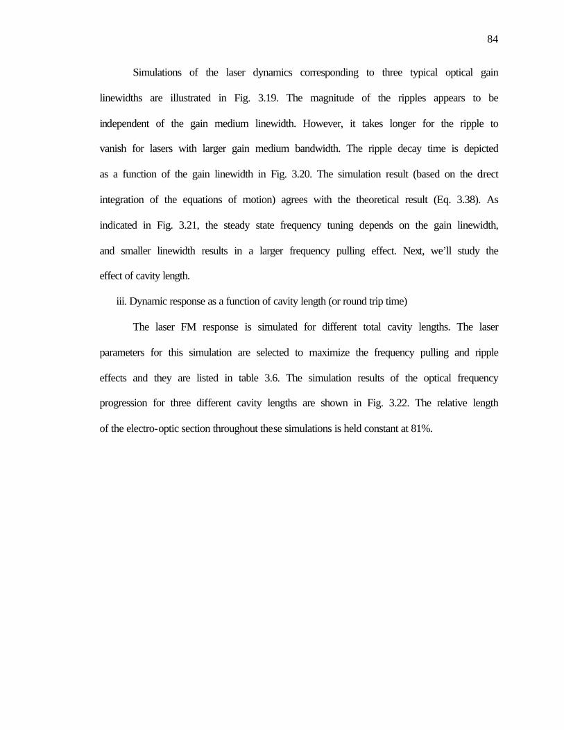
84
Simulations of the laser dynamics corresponding to three typical optical gain
linewidths are illustrated in Fig. 3.19. The magnitude of the ripples appears to be
independent of the gain medium linewidth. However, it takes longer for the ripple to
vanish for lasers with larger gain medium bandwidth. The ripple decay time is depicted
as a function of the gain linewidth in Fig. 3.20. The simulation result (based on the direct
integration of the equations of motion) agrees with the theoretical result (Eq. 3.38). As
indicated in Fig. 3.21, the steady state frequency tuning depends on the gain linewidth,
and smaller linewidth results in a larger frequency pulling effect. Next, we’ll study the
effect of cavity length.
iii. Dynamic response as a function of cavity length (or round trip time)
The laser FM response is simulated for different total cavity lengths. The laser
parameters for this simulation are selected to maximize the frequency pulling and ripple
effects and they are listed in table 3.6. The simulation results of the optical frequency
progression for three different cavity lengths are shown in Fig. 3.22. The relative length
of the electro-optic section throughout these simulations is held constant at 81%.

85
Table 3.6: Parameters for total cavity length simulation
Parameters Value
Log(R): cavity loss 0.2
2C: Normalized single pass gain 1.5
⊥γ : Gain linewidth 50GHz
||γ : 1 / Upper level life time 1e+8
β: electro-optic modulator
sensitivity
10MHz/Volt
electro-optic section length 81% cavity length
(a) Cavity round trip: ps10=τ
Figure 3.22: The laser FM response vs. different cavity lengths or round trip times

86
(b) Cavity round trip: ps20=τ
(c) Cavity round trip: ps40=τ
Figure 3.22 (continued)

87
The laser response is a function of the cavity length. Both the theoretical analysis
(section 3.2), and extensive simulations indicate that shorter cavities will produce smaller
frequency ripples. In addition, from the simulation we can also conclude that the ripple
decay time is also a function of the cavity round trip time. With a 40ps cavity roundtrip,
the decay time is around 0.2ns. When the cavity round trip is reduced to 10 ps, the ripple
lasts less than 0.05 ns. Thus, to obtain smooth FM response, the cavity round trip time
should be kept as small as possible.
3.4.3 Summary of laser response for varying voltage ramp and cavity parameters The laser dynamic response under voltage ramp excitation has the following
characteristics:
• The laser frequency response (shift) to the external ramp voltage signal
is practically instant
• The dynamic frequency response of the laser includes small ripples,
which have the period of cavity round trip time. These ripples intensify
with increasing slope of the applied ramp perturbation.
The laser cavity parameters also have significant influence on the laser
dynamic response.
• The relative length of the electro-optic segment should be kept as long as
possible to assure a smooth transient response (i.e., small ripple
amplitude) and higher tuning sensitivity. Ideally, the entire cavity should
be uniformly electro-optic.
• The ripple decay time decreases for narrower gain linewidths, but at the
expense of higher frequency pulling and lower tuning sensitivity.

88
• Shorter cavity lengths assure smaller ripples and more rapid convergence
to steady state. Therefore, a shorter cavity laser is preferred for laser
frequency tuning applications.
In the microchip laser system built in this thesis work, the ripples only introduce
very small changes to the phase of the optical field envelope. Thus, we can consider the
laser tuning response instantaneous, accompanied by an effective frequency noise (i.e.,
the ripples in the simulation). The noise level depends on the tuning speed, electro-optic
section length, and other factors enumerated above, and it is can be approximated using
the 0th-order theory for the electro-optic passive cavities (section 3.2) ,
cLLVn OEOE /))(,min // −Λ⋅⋅= &β
where V& is the ramp rate, Λ is the total cavity length, LE/O is the electro-optic section
length.
Next, we will discuss the microchip laser transmitter design issues and
experimental results.

89
Chapter 4: Tunable transmitter design
In this chapter, we will discuss the design and performance of the low noise
dynamically tunable mm-wave optical transmitter (DTMOT). First, we’ll provide the
DTMOT concept (section 4.1); then we’ll address the detailed design issues related to
single longitudinal mode (section 4.2) and single spatial mode operation (section 4.3) of
the microchip laser. The tuning of the microchip laser is covered in section 4.4 and
finally the experimental results are shown in section 4.5.
4.1 DTMOT concept
The original DTMOT concept is shown in Fig. 4.1, where P1 and P2 are two
independent pumps, G is the Nd:YVO4 gain section, M is the MgO:LiNbO3 phase
modulation section, E1 and E2 are electrodes.
Figure 4.1: The dynamically tunable millimeter wave optical transmitter structure

90
As indicated in Fig. 4.1, the mm-wave optical transmitter is based on optical
heterodyning of two electro-optically tunable single mode microchip lasers. The critical
component inside the DTMOT is the electro-optically tunable single-mode microchip
laser composite crystal assembly (Nd:YVO4 /Mgo:LiNbO3 from VLOC, Inc). The gain
section of the composite crystal is a 3% doped 0.2 mm thick Nd:YVO4 crystal. A 0.8 mm
long MgO:LiNbO3 crystal acts as an intracavity phase modulator. Dielectric mirrors are
directly deposited on each side of the laser system to form a plano-plano resonator. Two
side-by-side laser sections are implemented inside a single microchip laser crystal by two
independently driven 808 nm pump laser diodes. The Nd:YVO4 provides a homogenous
gain medium that may lead to multimode lasing in the presence of spatial hole burning.
However, the short pump absorption length [21] reduces the chance for spatial hole
burning thus assuring single mode lasing. In addition, the pump beam produces a weak
thermal waveguiding effect [23] in the Nd:YVO4 resulting in a single transverse mode in
the cavity. Two electrodes are deposited on the top and bottom of the MgO:LiNbO3
section for the tuning signals. The outputs of the two lasers are combined, coupled into a
single mode fiber, and transmitted to a high-speed photodiode, where the optical signals
heterodyne resulting in a microwave or millimeter-wave signal. The monolithic
configuration gives the device simplicity, and compactness. Originally we expected that
these two lasers in one crystal configuration assured a better stability, and reduced
sensitivity to external temperature fluctuations. However, later we found that the beat
frequency fluctuations caused by the external temperature fluctuations can be reasonably
controlled by simple electronics. Having two lasers separated, we enjoy the benefit of
easily setting the operating frequency from 0 to over a hundred GHz by temperature

91
tuning (section 4.42). Therefore, in the later implementations, two tunable lasers are in
separate crystals, which are independently temperature controlled.
The physical implementation of the transmitter is shown in Fig. 4.2. This
configuration consists of a 0.2 mm long Nd:YVO4 crystal (the gain medium) and a 0.8
mm long MgO:LiNbO3 crystal (the tuning section). The laser has an 80mW threshold and
a slope efficiency of better than 20%.
Figure 4.2: The heterodyne transmitter implementation
Important design considerations regarding this optical transmitter include laser
single (longitudinal and transverse) mode operation, frequency-tuning range, speed and
sensitivity, and noise. In this chapter, we are going to discuss these issues individually.
The laser efficiency issues are not going to be addressed here since they are well
represented in the literature [47].
92
4.2 Transmitter single longitudinal mode operation
Single longitudinal mode operation is a prerequisite for stable millimeter
heterodyne output. The single longitudinal mode operation is determined by the cavity
geometry (i.e., gain section length, and total cavity length).
Inside the microchip laser cavity, several cavity modes (~5 modes) are within the
gain bandwidth (200GHz). Although Nd:YVO4 is a homogeneously broadened gain
medium, one would expect that the inhomogeneous gain caused by spatial hole burning
[45] inside the F-P resonator will drive the laser into multimode operation. However, for
the electro-optically tunable microchip laser, the pump absorption only occurs in the
region very close to the reflection mirror where all the cavity modes have a common null
point. As a result, the localized inhomogeneous gain available to different cavity modes
is greatly reduced. To a certain extent, the cavity modes see mostly the same gain
medium and by modal competition only the mode closest to the gain center would
oscillate.
The single mode operation of microchip laser can be studied quantitatively by
normalized multimode operation threshold ζ(1,2) [21], which is the ratio of the maximum
single-mode inversion density of the laser medium to the lasing threshold inversion
density. The microchip laser operates in single longitudinal mode when pump power is
less than )2,1(ζ times laser threshold. Here ζ(1,2) is given by [21]:
11
][2
1 )2,1(
)2,1()2,1(
)2,1(
)2,1()2,1()2,1( −
><−
><−×
><−
><−=
ψ
ψβ
ψ
ψβζ (4.1)
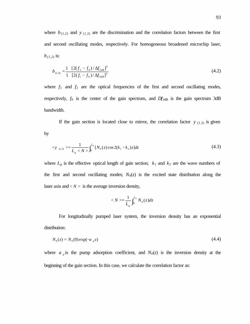
93
where β (1,2) and ψ(1.2) are the discrimination and the correlation factors between the first
and second oscillating modes, respectively. For homogeneous broadened microchip laser,
β (1,2) is:
2301
2302
)2,1( ]/)(2[1
]/)(2[1
dB
dB
fff
fff
∆−+
∆−+=β (4.2)
where f1 and f2 are the optical frequencies of the first and second oscillating modes,
respectively, f0 is the center of the gain spectrum, and ∆f3dB is the gain spectrum 3dB
bandwidth.
If the gain section is located close to mirror, the correlation factor ψ(1.2) is given
by
∫ −><
>=<gL
g
dzzkkzNNL 0 210)2,1( ])(2cos)([
1ψ (4.3)
where Lg is the effective optical length of gain section; k1 and k2 are the wave numbers of
the first and second oscillating modes; N0(z) is the excited state distribution along the
laser axis and >< N is the average inversion density,
∫>=< gL
g
dzzNL
N0 0 )(
1
For longitudinally pumped laser system, the inversion density has an exponential
distribution:
)exp()0()( 00 zNzN pα−= (4.4)
where pα is the pump adsorption coefficient, and N0(z) is the inversion density at the
beginning of the gain section. In this case, we calculate the correlation factor as:

94
)1()2(
)2sin2
2(cos1
2
22)2,1(g
g
L
ggL
ek
kLk
kLe
α
α
αα
αψ−
−
−∆+
∆∆
−∆−>=< (4.5)
where k∆ is the wave number difference between the first and second cavity mode.
As shown in Eqs. 4.1, 4.2, and 4.5, the single mode operation is a function of the
lengths of the entire cavity and the gain section, the rate of pump absorption, and the gain
medium bandwidth. The gain medium bandwidth is approximately 0.5 nm for Nd:YVO4.
The pump absorption rate is a function of Nd ions doping concentration. For the 3%
doped crystal used in the experiments the pump absorption rate is 100/cm [42].
The microchip laser single mode operation performance is studied for different
cavity structures using Eqs. 4.1, 4.2, and 4.5. The results are summarized in Figs 4.3, 4.4,
and 4.5. Fig. 4.3 depicts the multimode operation threshold of the microchip laser when
the lasing mode is aligned at the center of the gain spectrum. The single mode operation
under laser frequency tuning is shown in Fig. 4.4 and 4.5. The multimode operation
threshold vs. frequency detuning when total cavity length is 1 mm is depicted in Fig. 4.4,
while Fig. 4.5 depicts the multimode operation threshold vs. total cavity length when the
gain section length is fixed (0.2 mm)

95
Figure 4.3: Multimode operation threshold vs. total cavity lengths and gain section length
Figure 4.4: Multimode operation threshold vs. frequency detuning and gain section length
96
Figure 4.5: Multimode operation threshold vs. frequency detuning and total cavity length
Discussion
i. The cavity geometry for single mode operation
Short cavity geometry, especially short gain section, provides for better single
mode operation. As indicated in Fig. 4.3, the single mode operation depends very
strongly on the gain section length. Specifically, for a 0.2 mm 3% doped Nd:YVO4 gain
section, the laser will remain single mode even when the pump power is 10 times larger
than laser threshold. Therefore, we selected 0.2 mm gain section in the tunable microchip
laser system.
ii. The tuning range considerations
The multimode operation threshold decreases when the lasing frequency is
detuned from the gain center. Without exception, when the frequency detuning is one half
97
of the cavity FSR, the multimode operation threshold becomes unity, which indicates the
onset of the second lasing mode. Therefore the continuous frequency tuning range is
always smaller than cavity FSR.
A very interesting point from Fig. 4.5 is that the single mode performance under
normalized frequency detuning (with respect to cavity FSR) is not a strong function of
the overall cavity length. Extensive simulations show that this statement holds when the
effective pump absorption length is short compared to the overall cavity length. Since
shorter cavity laser would have larger FSR, it will have a better frequency tuning range.
iii. Effect of the dielectric mirror thickness
The high reflection (HR) dielectric mirror deposited on the gain crystal has finite
thickness, which introduces a small gap between the mirror reflection point and the
beginning of gain section (Fig. 4.6). To include this effect, Eq. 4.5 should be modified as,
)1()2(
)](2sin2
)(2[cos2sin2
2cos
2
22)2,1(gL
ggl
ek
dLkk
dLkedkk
dk
α
α
αα
ααψ−
−
−∆+
+∆∆
−+∆−⋅∆∆
−⋅∆>=< (4.6)
where d is the distance between the mirror reflection point and the start of the gain
section. Using Eq. 4.6, the effect of small gap on the laser single mode operation
performance is studied and the results are depicted in Figs. 4.7 – 4.9. Fig. 4.7 shows the
multimode operation threshold when the air gap is varied from 0 to 0.4 mm. Fig. 4.8 is a
close-in illustration of Fig 4.8. The max frequency tuning vs. different gap length is
shown in Fig. 4.9. The single mode operation depends strongly on the gap length. The
multimode operation threshold decreases by approximately 50% with 20 µm gap, which
is the typical mirror thickness. With a longer gap (>200 um), one would observe the onset

98
of multi-mode operation slightly above laser threshold. As a result, for microchip laser
design, the gap between the reflection point and gain section must be kept minimum.
Gain
d
Lg
L
M1 M2
Figure 4.6: The cavity structure where gap exist between the gain section and the mirror
Figure 4.7: The multimode operation threshold vs. gap length and gain section length

99
Figure 4.8: The multi-mode operation threshold vs. gap length ( 0.2 ~0.4 mm)
Figure 4.9: The multi-mode operation threshold vs. gap length and frequency detuning

100
4.3 The microchip laser transmitter single spatial mode operation
Single spatial mode operation is another important consideration for microchip
laser design. The microchip laser uses a plano-plano resonator structure and its spatial
mode is defined by the thermal effects of the pump beam (thermal lensing or thermal
expansion at mirror surface) [23]. In order to guarantee the single spatial mode operation,
the pump beam should have a smaller cross-section than the fundamental cavity lasing
mode. Otherwise, the unsaturated inversion density will provide gain for higher order
transverse modes, resulting in a possible multi-transverse mode operation. The single
spatial mode lasing limits the choice of pump system design.
Zayhowski et al. [23], postulated an expression for the microchip laser fundamental
mode cross section. However, their expression is not valid for the electro-optically
tunable microchip laser cavity, where two separate crystals exist and the pump absorption
only occurs inside the extremely short gain section (as seen in Fig. 4.10).
Thermal wave-guide Lg
Leff
Pump power
Thermal expansion
Figure 4.10: The conceptual laser cavity under the pump induced the thermal guiding and thermal expansion
Therefore, we derive an approximate expression (see appendix C) for the
fundamental mode cross-section ω for the tunable microchip laser:

101
4/1
4/1
)()
2
)0((
1
g
eff
c
eff L
L
nnk
P⋅
⋅⋅
⋅
⋅⋅≈
πλ
ααω (4.7)
where α is the heat-generating efficiency of the pump, P(0) is the absorbed pump power
density at the beginning of the gain section, kc is the thermal conductivity of the gain
crystal, n is the refractive index of the gain crystal, effα is the effective temperature
coefficient, and neeff n ααα +⋅= , where eα and nα are the thermal expansion coefficient
and refractive index temperature coefficient of the gain crystal, respectively, l and Leff are
the effective optic lengths of the gain crystal and the entire cavity, respectively.
Using Eq. 4.7, the fundamental spatial mode radius under different pump power
for a typical cavity configuration is simulated. The result for a microchip laser system
with 50 um pump radius, 0.2 mm long 3% doped Nd:YVO4, and 1 mm total cavity
length, is depicted in Fig. 4.11.
Figure 4.11: Fundamental spatial mode radius vs. different pump power

102
Pump spot size should be less than the fundamental spatial mode size for
guaranteed single mode operation. Hence, it is more advantageous to study the mode
cross section normalized with respect to the pump beam size. Fig. 4.12 depicts the
normalized spatial mode radius vs. different pump power levels and spatial modes for
microchip laser used in the experiment (0.2 mm long 3% doped Nd:YVO4 gain medium,
and 1 mm entire cavity length). When the laser operates in the area above the dotted line
inside Fig. 4.12, where the pump beam is smaller than the lasing mode cross section,
single spatial mode operation is guaranteed.
Figure 4.12: The normalized spatial mode radius vs. different pump power level and spatial mode

103
As indicated in Fig. 4.12, small pump size is desired for microchip laser single
spatial mode operation. However, there is a trade off. Smaller pump size generally means
more complicated pump optics. From Fig. 4.12 we note that a 50 um diameter pump
beam would lead to single spatial mode operation up to 700 mw pump power, which is
adequate for most realistic systems. Thus, a pumping system using 50 um diameter wide
pump diode butt-coupled to the gain section represents a suitable solution for the E/O
tunable microchip laser system. However, we are unable to obtain such diodes in an open
heat sink package suitable for the laser system. This leads to unwanted multi-spatial
operation at a higher pump level in the experiments.
4.4 Laser tuning
In this section we discuss the voltage, pump power and temperature tuning of the
microchip laser. The discussion here is based on the steady state behavior of microchip
lasers.
4.4.1 Electrical voltage tuning sensitivity Voltage is the desired tuning mechanism of the microchip laser because it has
rapid frequency response and it is highly linear. When voltage is applied across the
LiNbO3 section of one microchip laser, the effective cavity length, and thus the resonant
optical frequency changes by:
dV
lnlnln
frnf optical2211
1133
212 +
⋅⋅=η
δ (4.8)
where n1 is the refractive index of the extraordinary wave in the LiNbO3 section, n2 is the
refractive index of a π polarized wave in the Nd:YVO4 gain section, l1 is the electro-optic
section (LiNbO3) length, l2 is the gain section (Nd:YVO4) length, d is the thickness of the

104
LiNbO3 section, r33 is the LiNbO3 electro-optic coefficient along the z-axis, foptical is the
optical frequency, η is the overlap efficiency between the applied electric field and laser
cavity mode, and V is the applied voltage.
Eq. (4.8) indicates an ideal linear relationship between the frequency tuning and
applied voltage. The FM sensitivity is linearly proportional to the optical frequency
(inversely proportional to the optical wavelength). The wavelength dependence implies a
30% higher sensitivity at 1.06 µm compared to 1.32 µm wavelengths. It needs to be
pointed out that the FM sensitivity does not depend on the absolute length of tuning
element. However, as Eq. 4.8 indicates, it is a function of the ratio between the effective
optical lengths of E/O tuning section ( 11ln ) and entire laser cavity ( 22ln + 11ln ).
Specifically, if we have 0.2 mm long gain section and 0.8 mm long 0.5 mm thick tuning
section, and we consider the 1.06 µm lasing wavelength, the theoretical voltage tuning
sensitivity is 36 MHz/volt assuming 100% overlap between the electric and optical fields.
4.4.2 Temperature tuning sensitivity The absolute laser frequency is extremely sensitive to external temperature
variation. Accurate modeling of external temperature induced laser frequency variation
involves the numerical solution of temperature field equation inside the laser cavity with
proper boundary condition, which is beyond the goal of the thesis work. However, if we
assume that the microchip laser crystal has a constant temperature T along its boundary,
the temperature induced laser frequency variation satisfies:
opticaloptidal flnln
TlnTlnlTnlTnf ⋅
++++
=2211
22112211 )()()()( δδδδδ (4.9)

105
The thermal expansion coefficients of MgO:LiNbO3 and Nd:YVO4 are 2.0×10⁻⁶ K-1 [48]
and 7.2×10⁻⁶ K-1, respectively[49]. The temperature induced refractive index variation
coefficient is 6.7×10⁻⁵ K-1 for MgO:LiNbO3 [48] and 3.9×10⁻⁶ K-1for Nd:YVO4 [49]. The
calculated thermal tuning sensitivity is 13 GHz/oK. This model is overly simplistic since
the microchip laser crystal has only one surface bonded to the heat sink. Therefore, we
can control the temperature of only one surface and the actually thermal sensitivity could
be significantly smaller. However, the prediction from the simple model still provides a
good estimate. Accurate temperature tuning sensitivity is to be determined by experiment
(section 4.5.2).
4.4.3 Sensitivity to pump power tuning Pump power variation will introduce localized tempareture variation inside the
laser crystal, which will change the refractive index and therefore modify the cavity
resonance condition and hence the optical frequency [50]. For tunable microchip lasers,
signficant FM could be achieved with very small amplitude variations. In addition, pump
power tuning is useful in setting the transmitter initial frequency. A comprehensive
theorectical modeling on pump power tuning is given by Zayhowski et al. [50]. We will
determine the pump power tuning experimentally as shown in the subsequent sections.
4.5 Laser transmitter characterization
4.5.1 Laser threshold and efficiency A microchip laser is fabricated using a 0.2 mm 3 atom% doped Nd:YVO4 gain
section and a 0.8 mm MgO:LiNbO3 phase modulator section. By depositing two different
dielectric coatings (1064 nm HR / 1064nm 98%R, and 1034 nm HR/ 1034nm 99% R),
both 1064nm and 1340 nm microchip lasers are fabricated. The microchip lasers are

106
directly pumped by 808nm 1W open heatsink laser diodes (Spectra-physics SCI100-808-
z1-01). The microchip laser optical output power was measured for different pump
current levels, and the result is plotted in Fig. 4.13. The threshold of the 1064nm laser is
approximately 80mW pump power and its slope efficiency is 20%. The threshold and
slope efficient of the 1340 nm laser is slightly inferior (threshold: 95mW, Slope: 16%)
due to the smaller emission cross section [42] of Nd ions at 1340 nm.
Figure 4.13: The microchip laser threshold and slope efficiency characteristics

107
4.5.2 Optical spectrum quality and spatial quality
The optical spectrum of the microchip laser was investigated using an Ando
optical spectrum analyzer and Fig. 4.14 illustrates a typical optical spectrum.
Figure 4.14: Laser spectrum at 1063.6 nm
The resolution bandwidth of the optical spectrum analyzer is 0.1 nm, and the free
spectral range of the microchip laser is 60GHz (0.2 nm in terms of optical wavelength).
Therefore the optical spectrum analyzer is capable of resolving individual longitudinal
modes. In the optical spectrum measurement (Fig. 4.14a), only one peak exists, which
indicates single longitudinal mode operation. However, it should be mentioned here that
multi-mode behavior has been observed when the lasing mode is tuned (by temperature)
to the region close to the mode hopping frequency. This behavior is caused by the small
mode discrimination and it agrees with the theoretical predictions.

108
The microchip laser spatial profile was inspected first visually, and then a
microwave spectrum analyzer was employed to identify more accurately the occurrence
of multiple transverse modes by observing the possible beat signal between different
transverse modes.
Figure 4.15: A transverse mode beat tone captured by microwave spectrum analyzer.
In the visual measurement, the laser has a close to ideal circularly shaped beam
cross section at up to 6 times the threshold pump power. However, when measured by the
microwave spectrum analyzer, the transverse mode beating (~ 260MHz) is observed after
only 3 times the threshold pump power (Fig. 4.15). This agrees with our analysis, (section
4.3.2), since the simple direct laser diode pump produces a large elliptical pump beam
cross section (~100 µm diameter), which results in a smaller fundamental lasing mode

109
cross section and undeleted gain for higher order modes. Further improvement in pump
optics (small pump beam) would result in better transverse mode performance.
4.5.2 Microchip laser frequency tuning In this section, we discuss the microchip laser frequency tuning (voltage tuning,
temperature tuning and pump power tuning) characteristics.
i. DC voltage tuning sensitivity
Microchip laser voltage tuning has very fast response speed. Thus it is the primary
operation mechanism to generate a rapidly tunable mm-wave optical subcarrier using the
DTMOT. The voltage tuning sensitivity of the transmitter was characterized by
measuring the heterodyne signal frequency in the microwave domain versus the applied
voltage. Varying the voltage from 0 to 350 volt we measured a 7.7 GHz variation in beat
frequency, corresponding to a tuning sensitivity of 22 MHz/Volt, as shown in Fig. 4.16.
The difference between the measured and theoretical sensitivities (32 MHz/Volt for this
specific crystal) is caused by the inadequate field overlap and parasitic piezo effects of
LiNbO3. Further improvement in tuning sensitivity can be made by reducing the
thickness of the modulator. The sensitivity is ultimately limited by the breakdown voltage
of LiNbO3 (10kV/mm), which is 10 times larger than the current maximum tuning field.

110
Figure 4.16: Voltage tuning sensitivity
ii. Microchip laser temperature tuning sensitivity
The microchip laser frequency is very sensitive to the temperature variation,
although the tuning by temperature has a very slow response speed. Thus, we use the
temperature tuning to set the DTMOT operation offset frequency. The microchip laser
temperature tuning sensitivity is determined experimentally in the mm-wave / microwave
domain by monitoring the two beat tone frequency variation vs. the temperature of one
laser crystal. The result is shown in Fig. 4.17. With 6 degrees of temperature variation, a
37GHz beating tone tuning is observed and it reveals a sensitivity of 6.2GHz/C. The
measured temperature tuning sensitivity is about two times less than the calculated value
(13GHz/oC, as shown in Eq. 4.4.2) and it is a result of the overly simplistic theoretical
model, which assumes that all the surfaces of the crystal have the same temperature.

111
Figure 4.17: The frequency of the two laser beat signal as a function of the temperature
iii. Microchip laser pump power tuning sensitivity
The microchip laser frequency is also sensitive to the pump power variation.
Since the pump tunes the laser frequency via the localized temperature field variation
induced by pump power[50], it has a faster response than overall temperature tuning. In
the DTMOT, pump power tuning can be used to set and stablized the offset frequency.
The disadvantage of pump power tuning is that it introduces parasitic amplitude
modulation.
The sensitivity to the pump power variation was experimentally determined by
raising the pump power of one microchip laser from 90 mW to 170 mW and measuring
the two laser beat frequency variation. The resulting 5.6 GHz frequency shift is shown in
Fig. 4.18, corresponding to a sensitivty of 70 MHz / mW.

112
Figure 4.18: Two-microchip laser beat signal vs. pump power change.
4.5.3 mm-wave operation potential Nd:YVO4 has a gain linewidth over 200GHz. In principle, the microchip laser can
operate at any frequency within this 200GHz, which implies a 200GHz subcarrier tuning
range. In a practical tunable microchip laser system, by tuning temperature and pump
power setting, we can set the difference frequency between the two lasers from 0 to
150GHz limited by the finite laser free spectrum range. Fig. 4.19 depicts an example of
the optical spectrum of the beat signal in the 120GHz range.

113
Figure 4.19: The optical spectrum of 120GHz subcarrier signal @ 1340 nm
4.5.4 Microchip laser chirp rate testing The microchip laser chirp rate is measured using the experimental setup shown in
Fig. 4.20. Two microchip lasers are used in the slew rate measurement. A high-speed
high voltage ramp signal is applied on one laser section to generate frequency chirping,
while the frequency of the other section is kept at constant level. The two laser sections
were initially set to generate a heterodyne frequency of 12.9GHz. Heterodyning transfers
the optical domain chirping into the microwave domain chirping that is more
conveniently detected by a microwave homodyne frequency discriminator [51]. A very
low frequency component of the discriminator output (<100Hz) is selected and feedback
to the laser driver to stabilized the heterodyne signal frequency.
The microwave homodyne discriminator response is calibrated and the result is
shown in Fig. 4.21. The discriminator response is nonlinear (sinusoidal). Close to the
ideal operation point, the discriminator response is 0.9mV/MHz. Fig. 4.22 reveals the

114
discriminator output signal when, a 20 MHz, 10 V peak-to-peak triangular signal is
applied to the laser. The recovered signal, lower trace in Fig. 4.22, matches with the
applied voltage ramp, i.e., the upper trace. The scale of the lower trace is 100mV/
division, which indicates a 222MHz frequency excursion based on the discriminator
characteristics. Therefore, a frequency excursion of 222 MHz over a 25 ns time period
was measured, and a chirp rate of 8.8 GHz/µsec is achieved. It should be emphasized that
the available voltage ramp generator currently limits the chirp rate, but the transmitter is
capable of producing higher speed chirps, if required.

115
LD pump 1
LD pump 2
LD controller
Ramp Generator
Digital Oscilloscope
Microwave Hybrid
Variable delay line
Mixer Low pass filter
Fiber Optical Coupler
High-speed PD
Microwave power splitter
Microwave spectrum analyzer
Chirp detection
Figure 4.20: The microchip laser chirp rate measurement system
115
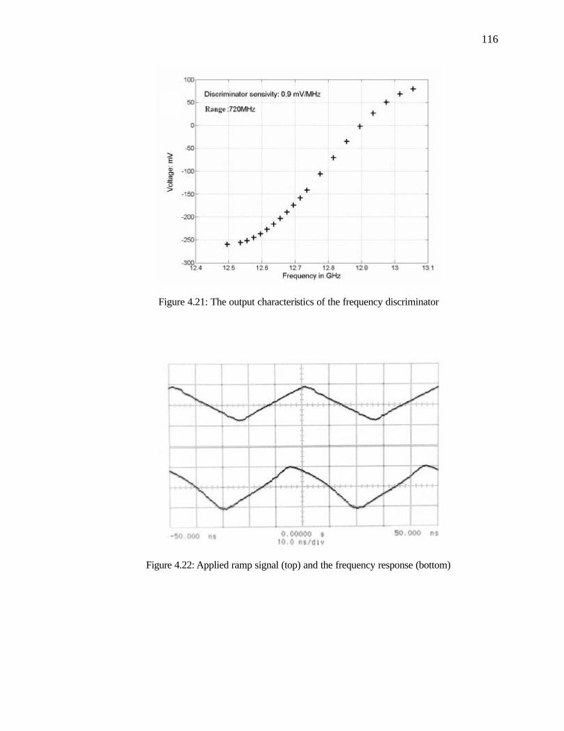
116
Figure 4.21: The output characteristics of the frequency discriminator
Figure 4.22: Applied ramp signal (top) and the frequency response (bottom)

117
4.5.6 The free running phase noise of the tunable transmitter In the laser heterodyning process, the microchip laser optical phase noise will be
downconverted into the mm-wave subcarrier domain. As shown in the next chapter, a
phase noise control system is required to obtain a clean beat tone. In this subsection, we
will determine the free running phase noise of the tunable transmitter, which is vital
information in designing the phase noise control system as shown in the next chapter.
The experimental setup for the laser phase noise measurement is depicted in Fig.
4.23.
Laser 1
Laser 2 PD
PLL Bandwith<50kHz
Microwave spectrum analyzer
1.04GHz
Figure 4.23: The laser phase noise measurement setup
As shown in Fig. 4.23, a PLL with very small closed loop bandwidth is employed
to stabilize the frequency drifting of the beat tone. With the PLL in place, the free
running phase noise is given by,
)()()( 22
2 ωφωωφ beatloopclosedfree H ⋅=
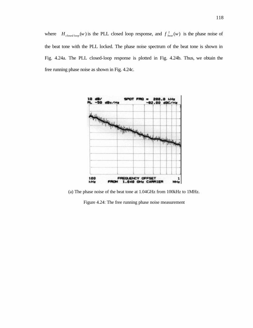
118
where )( ωloopclosedH is the PLL closed loop response, and )(2 ωφbeat is the phase noise of
the beat tone with the PLL locked. The phase noise spectrum of the beat tone is shown in
Fig. 4.24a. The PLL closed-loop response is plotted in Fig. 4.24b. Thus, we obtain the
free running phase noise as shown in Fig. 4.24c.
(a) The phase noise of the beat tone at 1.04GHz from 100kHz to 1MHz.
Figure 4.24: The free running phase noise measurement

119
(b) The PLL open loop response from 100kHz to 1MHz.
(c) The calculated free running phase noise spectrum from 100kHz to 1MHz.
Figure 4.24 (continued)
Limited by the minimum PLL bandwidth, we only measured the phase noise
spectrum from 100kHz to 1MHz. As shown in Fig. 4.24, the phase noise @ 100kHz
offset is –70dBc/Hz and the phase noise spectrum has a slope of -40dB/dec. The

120
experimental results (the shape of the phase noise spectrum) in Chapter 5 suggest that
40dB/dec is still valid below a 100kHz offset. Therefore, we estimate that the phase noise
at 10kHz offset should be –30dBc/Hz.
However, the measured slope rate of the phase noise spectrum is –40dB/dec,
which does not comply with results (i.e., –20dB/dec slope) for the quantum noise limited
laser system. One possible cause is the thermal vibration of the crystal lattice. However,
at this stage, we are unable to confirm this explanation.
4.6 Summary
The dynamically tunable mm-wave optical transmitter employing electro-optical
tunable microchip laser heterodyning is designed and tested. The issues regarding single
longitudinal mode operation, single spatial mode operation, and frequency tuning are
addressed in detail. By applying different dielectric mirror coatings, both 1.06 um and
1.34 um wavelength lasing have been achieved. The transmitter has very wide tuning
range (>100GHz) and good voltage tuning sensitivity (20MHz/volt). The transmitter
(laser) tuning speed is characterized using a 10MHz 20Volt ramp signal. In contrast with
the conventional laser intensity modulation, the tuning response is not limited by laser
relaxation oscillation (~1MHz). No speed limitation imposed by laser dynamics is
observed, which agrees with the theoretical prediction of Chapter 3.
In laser heterodyning, the laser phase noise and frequency jitter are directly
downconverted to the subcarrier. For low noise operation, a noise control subsystem is
required. In the next chapter, we’ll discussion the noise control techniques for this
heterodyne transmitter.

121
Chapter 5: Transmitter phase noise control subsystem
The dynamically tunable mm-wave optical transmitter (DTMOT) is conceptually
an ideal voltage controlled oscillator with high-speed and very large tuning range.
However, its free running phase noise is high because the heterodyning process directly
converts the laser phase noise into the mm-wave subcarrier domain. In order to generate a
low noise subcarrier signal, a phase noise control subsystem must be introduced. In this
chapter, we’ll discuss two distinctive yet conceptually related subsystems designed for
the dynamic tunable transmitter phase noise control, namely (1) digital frequency
synthesizer (section 5.1), and (2) delay line optical frequency locking loop (OFLL)
(section 5.2). The emphasis is placed on the OFLL subsystem due to its superior
performance at higher frequencies. Finally, we will present the experimental results
regarding noise suppression (section 5.3).
5.1 Digital frequency synthesizer
We first discuss the digital frequency synthesizer phase noise control subsystem.
A simplified synthesizer diagram is depicted in Fig. 5.1.

122
PD Phase Detector
N Counter
Reference fref1
R Counter
Loop Filter
Prescaler
Output
Optional 2nd reference: fref2
Modulation Signal
DTMOT
Figure 5.1: The digital frequency synthesizer
Except for the fact that the voltage-controlled oscillator is replaced by the
DTMOT, the digital frequency synthesizer phase noise control subsystem is identical to a
conventional digital synthesizer [52], the output of which is:
21 refrefout ffR
NPf +⋅
⋅= (5.1)
where P is the prescaler dividing number, and N and R are the counting numbers of the N
counter and R counters, respectively. In the following, we’ll briefly discuss the issues that
are pertinent to the digital synthesizer phase noise control system.
5.1.1 Synthesizer subsystem phase noise The noise sources of the output signal phase noise of synthesizer subsystem are:
the downconverted microchip laser phase noise, upconverted reference phase noise, pre-
scalar and counter jitter/phase noise, and AM noise from other electronic components
converted into PM noise [52]. Mathematically, the combined noise is given by,
)()()()()()()()( 222222
21
22 ωφωφωφωφωφωφωφωφ AMPRNrefrefopticalout ++++++= (5.2)

123
The seven terms on the RHS of Eq. 5.2 are the phase noise contribution from the laser
optical phase noise, reference 1 phase noise, reference 2 phase noise, N counter phase
noise/jitter, R counter phase noise/jitter, prescaler phase noise / jitter, and total amplitude
noise of the electronic components respectively. They are listed as [52]:
)]()([)(1
1)( 2
22
1
22 ωφωφ
ωωφ MLMLoptical H
++
= (5.3a)
)()(1
)( 21
222
1 ωφω
ωφ nref R
NPH
H ⋅⋅
+= (5.3b)
)()(1
)( 22
22
2 ωφω
ωφ nref H
H⋅
+= (5.3c)
)()(1
)()( 222
2 ωφω
ωωφ NeffN RNP
HH ⋅⋅+
= (5.3d)
)()(1
)()( 2Re
22
2 ωφω
ωωφ ffR RNP
HH ⋅⋅+
= (5.3e)
)()(1
)()( 222
2 ωφω
ωωφ PeffP PH
H ⋅+
= (5.3f)
)()(1
/)(
22 ω
ωω
ωφ nH
jkVAM +
= (5.3g)
where H(ω) is the open loop gain of the feedback system; 12
MLφ and 22
MLφ are optical
phase noise of the first and second microchip lasers; 12
nφ and 22
nφ are phase noise
contributions of the first and second reference sources; Neff2φ , ffRe
2φ and Peff2φ is the
effective phase noise of N counter, R counter, and prescaler; and )(ωn is the effective
amplitude noise of the electronic system at loop filter output; and, kV is the transmitter
voltage tuning sensitivity.

124
As indicated in Eq. 5.3, higher open loop gain would reduce the phase noise
contribution from the laser. However, the other phase noise inputs are nearly independent
of the open loop gain. For a well-designed system, the noise from the reference source
represents the ultimate performance limit, which increases 20dB per decade with
increasing frequency. This is the principal disadvantage of the digital synthesizer (PLL)
phase noise control system.
5.1.2 Frequency modulation within digital synthesizer subsystem Based on Fig. 5.1, the modulation response of the PLL can by calculated as,
)(1)(
)(ω
ωω
HkV
f Vout +
⋅= (5.4)
Since the open loop gain H(ω) is lowpass, in order to accommodate direct
modulation, the signal bandwidth should be larger than the PLL open loop gain
bandwidth. Table 5.1 summarizes the advantages and disadvantages of the digital
synthesizer approach.
Table 5.1: The advantage and disadvantages of the digital synthesizer approach
Advantages Disadvantages * Simple low cost circuitry.
* Direct control of output frequency.
* Relatively fast frequency selection.
* Automatic recovery from loss of lock.
* Frequency accuracy determined by reference
* Phase noise increases at 20dB/decade with
increasing output frequency.
* Jitter and noise of PLL dividers translates to
phase noise
* Digital electronics is difficult to obtain at high
frequency range

125
The digital frequency synthesizer works well at lower frequencies (<20GHz).
However, as the frequency increases, this approach becomes less suitable. In order to
generate high frequency, high quality signal, we propose a delay line optical frequency-
locking loop (OFLL). In the next section, the OFLL concept and design issues are
explained.
5.2 The delay line optical frequency-locking loop
The conceptual diagram of the delay line optical frequency-locking loop (OFLL)
is depicted in Fig. 5.2, where the DTMOT is also treated as a voltage controlled oscillator
(VCO). The output of the VCO is split into two paths. The signal in the first path is
detected by a high-speed photo diode (PD), while the signal in the second path is detected
after a long delay though a single mode fiber. The VCO phase error is recovered by
mixing the outputs from the two paths, and then fed back into the VCO (DTMOT) via a
special loop filter. Unlike the conventional synthesizer, the OFLL does not need a
reference source to recover and correct the phase / frequency error from the VCO.
Instead, it is accomplished by optical processing (the homodyne delay). In the
subsequent sections, we’ll discuss the OFLL operation principle, practical
implementation concerns, and OFLL system level design.
3dB Coupler
PD2 PD1
Loop Filter
Delay line frequency / phase discriminator (DFPD)
Fiber stretcher
Direct Modulation
DTMOT
Figure 5.2: Delay line optical frequency locked loop (OFLL)
126
5.2.1 OFLL operation principle In this section, we discuss the OFLL principles:
i. Mathematic modeling
ii. Frequency tuning and modulation scheme
iii. Noise performance
Each of these will be discussed in subsequent sections.
i. An analytic model for the OFLL
As a first step, we present the mathematical model for the delay line homodyne
frequency discriminator (DFD). The output of the delay homodyne discriminator is given
by,
])()(cos[)]()(1[)( 021 τωτφφτ +−−−++⋅= tttntnAAktV nnmo (5.5)
where mk is the mixer nonlinear coefficient related to the mixer conversion gain, A1 and
A2 are the subcarrier amplitudes of the first and second paths, respectively, n(t) is
amplitude noise of the subcarrier, φn(t) is the subcarrier phase noise, and τ is the time
delay of the second (delayed) path.
In the steady state, the delay line discriminator has a vanishing DC output, which
implies that the DC phase offset (ω0τ) of the discriminator output should satisfy the
relation
)2/( ππτω += ko (5.6)
where k=0,+/-1, +/-2, … In addition, in order to maintain feedback stability, the k values
must be either all even or all odd depending on the polarity of the loop filter output. For
simplicity, we assume a negative polarity of the loop filter output (i.e., negative

127
feedback), k has to be even, i.e., ik ⋅= 2 , where i is an integer called the modal number
of the OFLL.
In the steady state (i.e., τππω /)2/2( +⋅= io ), the delay line homodyne
frequency discriminator output (Eq. 5.5) can be simplified as,
)]()([)( 21 τφφ −−×⋅= ttAAktV nnmo (5.7)
where the approximation ( θθ ≈sin , if 1<<θ ) is employed and the higher order terms
(the cross product between the phase and AM noise) are neglected.
It is more convenient to present Eq. 5.7 in the frequency domain,
)()1(])()([)( ωφωφωφω τωτω jekejjkjV nj
pj
nnpo ⋅−⋅=⋅−⋅= ⋅⋅ (5.8)
where 21AAkk mp = , and )( ωφ jn is the spectrum of the phase noise term )(tnφ .
Based on the frequency domain presentation of the delay line frequency
discriminator, the entire optical frequency locking loop system can be treated precisely as
a linear feedback control system, as shown in Fig. 5.3.
ODFD H(ω)=kp[1-exp(jωτ)]
TMOT (VCO): Kv/jω
φopt(jω)
Loop Filter F(jω)
no(jω)
φout(jω)
Figure 5.3: OFLL system block diagram

128
The tunable transmitter is considered as a voltage-controlled oscillator with free
running phase noise, the control of which is the principal task of the OFLL system. The
amplitude noise from the electronic components is modeled jointly as the equivalent
output noise )(0 ωjn of the delay line homodyne frequency discriminator. Next we
analyze tuning (i.e., slow variation of operating frequency) and direct modulation (i.e.,
rapidly frequency modulation by applied analog or digital signal) of the OFLL.
ii. OFLL frequency tuning and direct modulation
The OFLL operation frequency can be tuned by,
• Mode hopping
• Delay time tuning by the fiber stretcher
The first method changes the frequency in stepwise fashion with a resolution
given by,
τπ /2=FSR
The second method continuously changes the operating frequency, however, its range is
limited by the max fiber stretching,
Ll
⋅= 0ωδω
where 0ω is the current operating frequency, l is the max stretch of the stretcher, and L is
the total delay length. In order for the OFLL to cover the entire frequency range, the
stretcher tuning range has to be larger than delay line free spectrum range, which implies
the requirement for the minimum stretching length,
00
2λ
ωτπ
=⋅
>= Ll
(5.9)
129
where 0λ is the mm-wave subcarrier wavelength inside the fiber.
In the experiments discussed later, both mode hopping and fiber stretching were
employed to obtain a continuum of operating frequencies from 0 to over 40GHz.
Like the digital synthesizer system, the OFLL can be directly modulated. The
OFLL direct modulation is given by,
)(1)(
)(ω
ωω
GV
kf Vout += (5.10)
where G(jω) is the system open loop gain,
ωωω ωτ iFekkG ipv /)()1()( −−= (5.11)
In order to accommodate the direct modulation of the OFLL output signal, the
modulation frequency must be larger than the OFLL open loop cutoff frequency.
iii. OFLL noise performance
Using the OFLL linear system diagram (Fig. 5.3), its output phase
noise )(2 ωφ jout can be calculated as,
2
20
2
22
)(1
/)()(
)(1
)()(
ω
ωωω
ω
ωφωφ
G
iFkn
Gj vn
out+
⋅+
+= (5.12)
where F(ω) is the loop filter gain, kv is the VCO voltage tuning sensitivity
Under the desirable OFLL operation, G(ω) >> 1, Eq. 5.12 can be simplified as:
20
2
22
)1(
)(
)(
)()(
ωτ
ω
ω
ωφωφ
ip
nout
ek
n
G −−+= (5.13)
The first term on the RHS of Eq. 5.12 is defined as the residual phase noise,
which represents the phase noise contribution from the lasers. The second term describes
130
the phase noise contribution from the OFLL electronics, which is the noise floor of the
OFLL system. Two issues concerning the OFLL noise performance will be addressed
next. They are the suppression of the free running VCO phase noise, and the noise floor
of the OFLL.
(a) Suppression of free running VCO phase noise
Suppressing the free running VCO phase noise is the principal task of the OFLL.
A larger open loop gain provides better optical domain phase noise suppression.
However, the open loop gain has to be carefully designed to satisfy the stability
requirement. The system stability issue is to be addressed in detail in the loop filter
design section (Section 5.2.3).
(b) The OFLL noise floor
The OFLL noise floor is given by the noise from the electronic components. In
this section, the OFLL noise floor is calculated analytically.
From Eq. 5.11, the OFLL noise floor is given by,
2_1
)(ωτ
ωφi
floornoisee
NEPj
−−= (5.14)
where NEP is defined as the noise equivalent power per Hz at the discriminator output,
pkjnNEP /)(0 ω= .
If we neglect the flicker noise (<1kHz), the following electronic system noise
sources contribute to the overall noise at the output of the delay line homodyne frequency
discriminator:
The thermal noise [53] from the mth path: mmBmT GNFTkn ⋅⋅=
The shot noise [54] from the mth path: mmpdms GRIen ⋅⋅⋅= 2

131
The equivalent input noise of loop filter: nfilter
where kB is the Boltzman constant, T is the temperature in Kelvin, Ipd is the photocurrent
of the photodiode, R is the termination impedance (50 ohm) of the PD, NFm is the noise
figure of the mth path, and Gm is the gain of the mth path. The total noise power is given
by combination of all these noise contribution,
∑ ⋅⋅⋅+⋅⋅+=m
mmpdmmBfilter GRIeGNFTknn )2()(0 ω (5.15)
where the total signal power is given by:
impdv GRIk ⋅= 2)( , 2 1,m = (5.16)
Neglecting the loop filter noise, which is always the case for a well-designed
OFLL loop filter, we obtain the formula for the OFLL system noise floor as shown,
2
2_ )exp(1/)(2
)( ωτωφ iRI
RIeNFTk
m pdm
pdmm
Bfllornoise −
⋅⋅+⋅
= ∑ (5.17)
Three distinctive features of the OFLL system are revealed in the analytic
expression for the noise floor. First, the OFLL noise floor depends on optical power (i.e.,
photocurrent Ipd). At a lower optical power, the noise floor is thermal noise limited (20dB
decrease per 10 times increase in optical power). At a higher optical power, the noise
floor is limited by shot noise (10dB decrease per 10 time increase in optical power).
Secondly, the noise floor strongly depends on the OFLL delay time, τ. A longer
time delay means better close-in carrier phase noise performance. However, a longer
delay also results in smaller mode spacing, which leads to deterioration of the phase noise
far away from the carrier frequency. More importantly, as we’ll see in the loop filter
design section, a longer delay time reduces the maximum loop stable gain and poses
serious challenge for the design of the high gain loop filter.

132
Finally, the OFLL uses the fiber delay time as a frequency reference. If we
neglect the stochastic variation of the fiber delay time, the OFLL output noise is a strong
function of the signal-to-noise ratio at the delay line discriminator output. The OFLL
noise floor does not depend on the laser RIN assuming that the balanced mixer is ideal.
However, in practice, the balanced mixer is not and therefore it converts the laser RIN
into subcarrier phase noise, which contaminates the signal spectrum. In the following
sub-section, a special technique is introduced to suppress this unwanted effect.
5.2.2 OFLL implementation using a non-ideally balanced mixer The OFLL conceptual diagram (Fig. 5.2) is overly simplistic in terms of practical
implementation. A practical balanced mixer at higher frequencies is not ideally balanced,
thus it introduces a subcarrier AM noise into the frequency discriminator output, and
significantly raises the OFLL phase noise floor. For a non-ideally balanced mixer, the
homodyne discriminator output becomes,
))(21())(21(])()(sin[)( 222
211021 ττωτφφ −+++++−−⋅= tnAktnAkttAAktV nnmo
(5.18)
where k1 and k2 are constants related to the non ideally balanced mixer.
The DC term in Eq. 5.18 can be compensated for by a proper input offset in the
OFLL loop filter. The AM noise term, however, will contaminate the phase noise
spectrum. In this section, we’ll discuss an OFLL implementation scheme (shown in Fig.
5.4) that suppresses subcarrier AM-to-PM noise conversion due to an unbalanced mixer.

133
3dB Coupler
PD1
Loop Filter
Low frequency modulation signal
Direct Modulation
PD2
M1 M2 M3
Figure 5.4: The OFLL implementation scheme with reduced AM to PM noise conversion
In Fig. 5.4, the mm-wave carrier signal of the second (delayed) path is by a fixed
low frequency signal (fm) using mixer (double sideband up-converter) M1, whose output
is later mixed with the mm-wave carrier signal from the first path by the second mixer
M2, and the M2 output signal is mixed with the low frequency modulation signal to
recover the subcarrier phase error information. We can prove that using this approach
(see Appendix D), the amount of the reduction in the subcarrier AM noise to phase noise
conversion is given by,
dB )/A20log(A)x20log(Indeconversion PMAMin Reduction 21AM +=→ (5.19)
where AMIndex is the modulation index of the first mixer (modulator).
For a system with equal signal amplitude in both paths, the AM-to-PM noise
conversion is suppressed by 20 dB with 20 dB AM modulation index. This is sufficient
under most situations of interests.

134
5.2.3 OFLL loop stability and the loop filter design The principal task of the OFLL is to suppress the phase noise contribution by the
laser. In order to reduce the residual laser phase noise at the OFLL output, the OFLL loop
filter must provide a sufficient open loop gain without compromising the loop stability. In
this subsection, we address the issues on the OFLL loop filter design.
In the loop filter design, the principal difficulty emerges from the repetitious
phase response of the delay line homodyne discriminator, which periodically varies its
phase from –90 to +90. To deal with this periodic phase response, a unique loop filter
structure was devised as shown in Fig. 5.5.
F1(s ) C( s )
OFLL loop f i l t e r
Adjus tab le ga in
Figure 5.5: OFLL loop filter structure
The OFLL loop filter has three stages. The first stage is a compensation block,
which flattens the repetitious phase response of the homodyne discriminator; the second
block is standard prototype PLL loop filter; and the final stage is an adjustable gain. The
three filter design steps are identified as:
Step 1. Design a prototype PLL loop filter
Step 2. Design compensation block
Step 3. Check the stability, and loop gain

135
Next, we explain the loop filter design process for an OFLL with 150-meter delay.
Step 1. Prototype PLL loop filter
We choose a 3rd order PLL loop filter as our prototype filter (Eq. 5.20).
Considering a 150-meter fiber delay, which gives a free spectrum range of 1.33MHz, we
put the null of the prototype filter at 61033.3 × rad /sec (approximately at the center of the
frequency spectrum range related to a 150 meter delay). In addition, we set the pole
frequency to 71067.1 × rad / sec.
p
z
sss
sFω
ω/1
1)(1
+⋅
+= (5.20)
where ωz and ωp are the null and pole frequencies of the prototype filter respectively.
Step 2: Compensation block design
The basic idea regarding the compensation block design is to approximate the
sinusoidal term (i.e., )]exp(1[ ωτi− in Eq. 5.8) of the delay homodyne discriminator by a
rational system, and then using the inverse of the rational system as the compensation
block. We use lower order (<2) Pade approximation method [56] to approximate the
sinusoidal response. As a comparison, the compensation block is designed using both the
1st and 2nd order Pade method.
For a system with a 150-meter fiber delay, the delay time is 0.75 ns. Using the 1st
order Pade method, the sinusoidal term )] 75.0exp(1[ nsi ×− ω , can be approximated by,
61 10667.22
)(×+
⋅=
ss
sG (5.21)
Thus, the compensation block based on the first order approximation is the inverse of
)(1 sG ,
136
ss
sC⋅
×+=
210667.2
)(6
1 (5.22)
Similarly, the compensation block based on the 2nd order approximation can be calculated
as shown in Eq. 5.23.
7
6
2 106.1210667.2
)(×
+⋅
×+=
ss
ssC (5.23)
Compared with 1st order compensation, 2nd order compensation introduces an
additional differentiator (the last term of Eq. 5.23), which provides a 90-degree phase
lead at high frequencies. As will be shown later, the OFLL loop filter with 2nd order
compensation have approximately 13 dB more gain while maintaining the loop stability
due to the 90-degree phase lead.
Step 3: Check the loop stability and gain
The objective of the loop filter design is to achieve maximum open loop gain
without compromising the loop stability. The last step in the loop filter design is to
optimize the adjustable gain to attain the maximum suppression of the downconverted
optical phase noise. Fig. 5.6 depicts the Bode plot and Nyquist plot of the optimized open
loop response of OFLL system with 1st order compensation. Nyquist plot indicates a
stable system. However, the Nyquist tracer is very close to the unstable point (-1,0)
indicating the stable margin. The Bode plot reveals an open loop gain of 68 dB @ 10kHz
offset.

137
(a). Bode diagram of the optimized OFLL open loop response with 1st order compensation block. The open loop gain @ 10kHz is 68dB.
(b). Nyquist diagram of the optimized open loop gain.
Figure 5.6: The performance of the loop filter with 1st order compensation
In comparison, the Bode and Nyquist plot of the optimized 2nd order compensated
system open loop response is shown in Fig. 5.7. The Bode plot reveals an open loop gain
of –81.3 dB @ 10kHz offset, which is 13dB higher than the first order system, indicating
that the 2nd order compensation provide 13dB more optical domain phase noise
suppression. It occurs because the additional differentiator introduces an additional 90-
degree phase lead to compensate the phase lag from the VCO (DTMOT).

138
(a). Bode diagram of the optimized OFLL open loop response with 2nd order compensation block. The open loop gain @ 10kHz is 81.3dB.
(b). Nyquist diagram of the optimized (max gain) OFLL open loop gain. The Nyquist trace does not encircle the unstable point (-1,0), indicating a stable response.
Figure 5.7: The performance of the loop filter with 2nd order compensation
It should be mentioned that in principle higher order compensation (>2) should
allow higher loop gain, and result better optical domain phase noise suppression.
However, a higher order compensation block would introduce unstable behavior (poles in
the right hand s plane) and complicates the filter design process. In most situations, the
simple 2nd order compensation is sufficient.
In addition, extensive simulations were performed on the loop filters for different
fiber lengths. It was found that for both the first order and the second order compensated
loop filter, the maximum stable gain decreases 40 dB per 10 times increase in the fiber
delay length. Thus, even though increasing fiber delay length decreases the OFLL system
noise floor, it reduces the stable open loop gain and results in a significant increase in the
residual laser phase noise. Therefore, unless using an OFLL with multiple loops (see

139
Section 5.25), the length of the fiber delay needs to be carefully selected to trade off the
residual noise and the noise floor.
5.2.4 Design of the OFLL system using a single loop In this section, we are going to discuss the OFLL system design using single loop.
The results from the previous sections will now be applied to determine the OFLL system
parameters such as system configuration, total delay length, etc. First, the design
objective, namely, the phase noise, was identified. Then, based on the trade off between
the residual noise and the noise floor, we selected a suitable length of the fiber delay,
from which the parameters for the loop filter is determined.
i. OFLL design objectives
Table 5.2 summarizes the design objectives of the OFLL system and Table 5.3
summarizes the parameters of the DTMOT.
Table 5.2: The design objectives of a single loop OFLL
Requirements Objective
Output phase noise -80dBc @1kHz
-100dBc @ 10kHz
-120 dBc @ 100kHz
Operating frequency: DC to 40 GHz

140
Table 5.3: The parameters for the components in the single loop OFLL
Components Parameter
VCO
(Microchip laser assembly) voltsradkV //10*56.12 4=
VCO optical power 2dBm @ both wavelength
VCO free running phase noise
(Estimated)
-40 dB/ dec slope
-30 dBc @ 10kHz @ 10kHz (by estimation)
-70 dBc @ 100kHz
-110 dBc @ 1MHz
Photodiode output power @ delayed path -26 dBm
Photodiode output power @ direct path -21 dBm
Link noise figure 6dB
ii. Optimum delay length
The OFLL implementation scheme shown in Fig. 5.4 is employed. In order to
select the optimum length of the fiber delay, the phase noise performance corresponding
to different fiber delay lengths is depicted in Fig. 5.8.
Figure 5.8: OFLL system noise floor for different fiber delay lengths
141
As shown in Fig. 5.8, in the close-in carrier region the phase noise is limited by
the OFLL noise floor, and it has a decay rate of 20dB/dec. However, when the frequency
is further away from the center, the phase noise spectrum becomes flat, which indicates
that in this region the phase noise of the OFLL is dominated by the residual laser phase
noise (i.e., open loop gain limited). In order to optimize the phase noise from 10kHz to
100kHz region, a fiber length of 90 meters is selected, which yields the following noise
performance:
–88 dBc @ 1KHz, -108 dBc @ 10kHz, -118dBc @ 100kHz.
In addition, using the procedure in section 5.2.3, the loop filter for 90-meter fiber
delay employing a second order compensation block is given by,
73/1166s
s 2.667e0075.926e013 + s 1.333e007 + s
)(2
++⋅
++⋅=
esse
sF
In section 5.3, we will examine the experimental results for this single loop
OFLL. But next, we will discuss a more sophisticated OFLL architecture that allows
independent optimization of the open loop gain and the noise floor.
5.2.5 Multi-loop OFLLs In a single loop OFLL system, although a longer fiber delay lowers the noise
floor, it reduced the stable feedback gain and leads to a significant increase of the residual
phase noise. In this section, we introduce a multi-loop OFLL to eliminate this problem. A
general diagram of the multi-loop OFLL system is depicted in Fig. 5.9. Although the loop
filter for the longer loop is generally not necessary and can be eliminated to reduce the
system complexity, it is still considered because we want to obtain a general model for
the multi-loop system and it is found in the simulations that this filter does improve the
system performance.
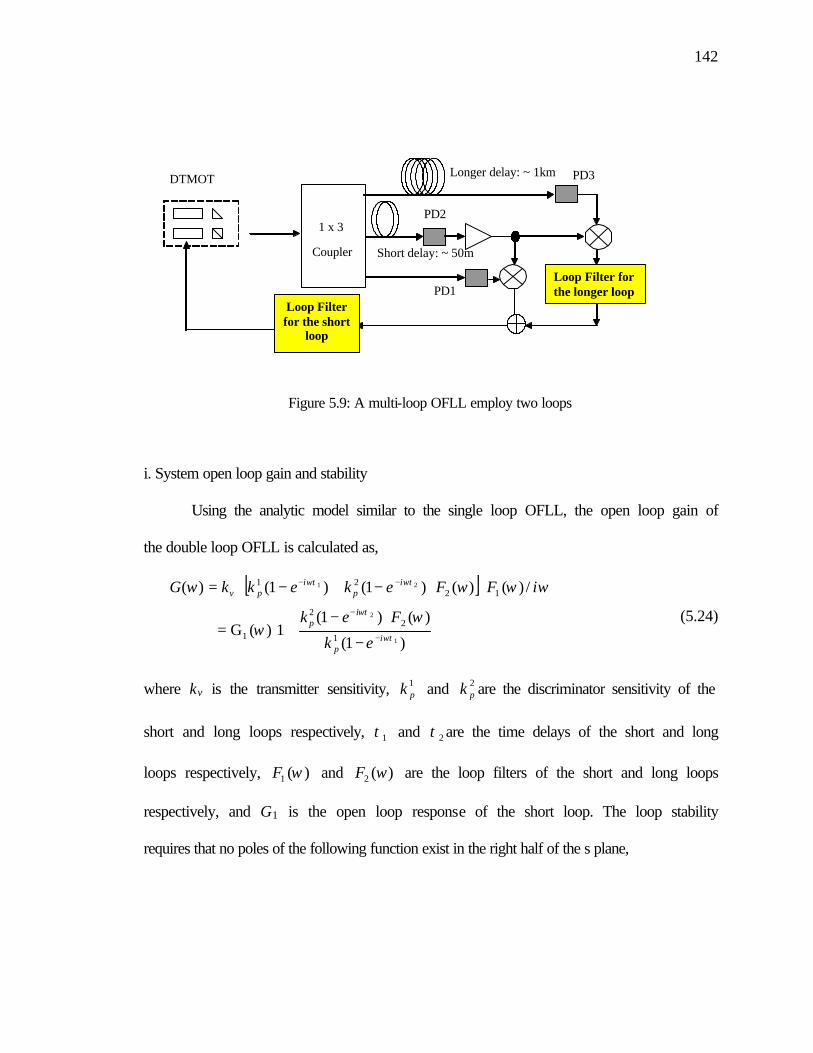
142
1 x 3
Coupler
PD2
PD1
PD3
Loop Filter for the short
loop
Loop Filter for the longer loop
Longer delay: ~ 1km
Short delay: ~ 50m
DTMOT
Figure 5.9: A multi-loop OFLL employ two loops
i. System open loop gain and stability
Using the analytic model similar to the single loop OFLL, the open loop gain of
the double loop OFLL is calculated as,
[ ]
−
⋅−+=
⋅⋅−+−⋅=
−
−
−−
)1(
)()1(1)(G
/)()()1()1()(
1
2
21
1
22
1
1221
ωτ
ωτ
ωτωτ
ωω
ωωωω
ip
ip
ip
ipv
ek
Fek
iFFekekkG
(5.24)
where kv is the transmitter sensitivity, 1pk and 2
pk are the discriminator sensitivity of the
short and long loops respectively, 1τ and 2τ are the time delays of the short and long
loops respectively, )(1 ωF and )(2 ωF are the loop filters of the short and long loops
respectively, and G1 is the open loop response of the short loop. The loop stability
requires that no poles of the following function exist in the right half of the s plane,

143
)(1
)1(
)()1()(G
1
1)(1
1)(1
1)(
1
1
22
11
1
2
ω
ωω
ωωω
ωτ
ωτ
G
ek
FekGGH
ip
ip
+
−
⋅−⋅
+
×+
=+
=
−
− (5.25)
Thus, the stability of the double loop OFLL system is determined by the stability of the
short loop OFLL (i.e., )(1
1
1 ωG+) and the stability of a seemingly more complex system
( )ωH~ ,
( )
)(1
)1(
)()1()(G
1
1~
1
1
22
1 1
2
ω
ωω
ω
ωτ
ωτ
G
ek
FekjH
ip
ip
+
−
⋅−⋅
+
=
−
− (5.26)
We called ( )ωH~ “stability function” of the Multi-loop OFLL. Although the
function ( )ωH~ looks complicated, it is well behaved. Extensive simulation indicates that
it is generally stable if the ratio between the lengths of the short loop to the longer loop is
below 20.
ii. The noise performance of the multi-loop OFLL
Just like its single loop counterpart, the multi-loop OFLL has an output phase
noise given by:
2
21
2
22
)(1
/)()(
)(1
)()(
ω
ωωω
ω
ωφωφ
G
iFkn
Gvon
out+
⋅+
+=
(5.26)
where nφ is the free running phase noise of the transmitter, and on is the equivalent input
noise at the discriminator for the short loop. The expression for phase noise of the multi-
loop OFLL has the same explicit form as that of the single loop OFLL. However in the

144
multi-loop OFLL, the equivalent input noise is the combination of the noise for both
loops.
The first term on the right hand side of the Eq. 5.26 is the OFLL residual phase
noise, and the second term is the noise floor. For the region close to the carrier frequency,
the open loop gain is much bigger than 1. Then, the noise loop for the multi-loop OFLL
can be simplified as,
2
221
2
)()1()1(
)()(
21 ω
ωωφ
ωτωτ Fekek
ni
pi
p
oout
⋅−+−=
−− (5.27)
Assuming equal carrier power in both loops and a unity filter for the longer loop,
it is shown in Eq. 5.27 that the noise floor of the double loop OFLL is determined by the
longer loop.
iii. A practical example of double loop OFLL
To conclude the discussion on the multi-loop OFLL, we discuss the design of a
double loop OFLL system employing 50 meter and 1km fiber delay.
The first step is to determine the filter parameters for the short loop. Applying the
result for the single loop OFLL, the loop filter with 2nd order compensation is given by:
7)s/5e(1 6/s)5e((s 7)/s)0.8e(s7(s/2.4e k F1(s) ++⋅++⋅++++⋅=
where k is the adjustable gain.
Ideally, the loop filter for the longer loop should be obtained in the same manner
as the short loop. But for simplicity of the circuitry, it is eliminated. As shown below,
good performance is still obtained this way. Assuming both loops have equal power, we
obtain the maximum stable open loop gain in Fig. 5.10. The Nyquist diagrams for the
open loop gain of both the short loop and the stability function )(~ ωjH are depicted in

145
Fig. 5.11. Both diagrams indicate a stable response. As shown in Fig. 5.10, the open loop
gain for the double loop OFLL at 10kHz is 129 dB.
Figure 5.10: The open loop response of the double loop OFLL at maximum stable gain.
(a) The Nyquist plot for the short loop
Figure 5.11: Stability of the multi-loop OFLL

146
(b) The Nyquist plot for the multi-loop stability function H~
Figure 5.11 (continued)
The noise floor of this double loop OFLL is calculated by assuming similar link
parameters as shown in table 5.3. The noise floor is found to be –130dBc/Hz at 10kHz
offset with a slope of –20dB/dec.
It should be pointed out that the multi-loop OFLL can include more than 2 loops
to further improve its performance. Their stability and noise can be similarly analyzed
using the techniques explored in this subsection.
Next, we will discuss the experimental result of the two noise control systems.
5.3 Noise control subsystem characterization
In this section, we discuss first the experimental results on the digital synthesizer
phase noise control subsystem and then the results on the OFLL.
5.3.1 Digital synthesizer type noise control The digital synthesizer type phase noise control subsystem is depicted in Fig.
5.12. Using the digital synthesizer, we lock the DTMOT output to a 133MHz ultra stable
reference source (Miteq XTO-05-133). Limited by the microwave prescaler, the digital

147
synthesizer has an operating range from 3GHz to 18GHz. The noise spectrum when the
DTMOT is operating at 8.447 GHz is depicted in Fig. 5.13, while Fig. 5.14 shows the
phase noise at 10kHz for different operating frequencies. The phase noise, as expected,
degrades with increasing carrier frequency.
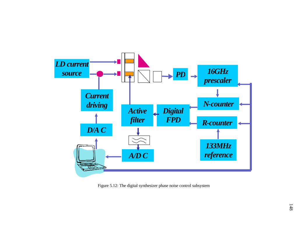
148
LD current
source
PD
Active filter
133MHz reference
N-counter
16GHz prescaler
R-counter
A/D C
D/A C
Current driving
Digital FPD
Figure 5.12: The digital synthesizer phase noise control subsystem
148

149
Figure 5.13: The digital synthesizer phase noise spectrum of 8.447GHz
Figure 5.14: The digital synthesizer phase noise vs. operation frequency

150
Using a secondary reference source, the DTMOT can be set to operate in the mm-
wave frequency range. The experimental setup is depicted in Fig. 5.15. The DTMOT
output is mixed down to 14GHz by a 26GHz low noise signal, and the 14GHz
downconverted signal is locked by the digital synthesizer. The phase noise measurement
was carried out at the lower frequency (14GHz) to eliminate the noise contribution from
the secondary reference source. The optical spectrum at 40GHz is revealed in Fig. 5.16.
The measured phase noise at a 10kHz offset is –90dBc/Hz (Fig. 5.17).
Mm-wave optical Transmitter
Digital synthesizer sub-system
26GHz Ref
PD
40 GHz
14 GHz
Set @ 14 GHz
Figure 5.15: The experimental scheme for 40GHz operation based on the digital synthesizer phase noise control

151
Figure 5.16: Optical spectrum of 40GHz subcarrier signal
Figure 5.17: Phase noise spectrum of the downconverted signal (14GHz)
The direct modulation of the digital synthesizer was also examined and the result
is illustrated in Fig. 5.18. In this experiment, the DTMOT is set to operate at 8.447 GHz.
A 3volt, 1.5MHz triangular wave signal is applied to the DTMOT which generates a

152
linearly chirped subcarrier signal, which is then demodulated by an Agilent vector signal
analyzer. The low speed is chosen since we are interested in identifying the lower bound
of permitted modulation signal and the digital synthesizer only limits the lower frequency
modulation signal [52] (i.e., < its loop bandwidth).
(a) Signal spectrum captured by an HP VSA.
(b) Instantaneous frequency
Figure 5.18: The response of the digital synthesizer under direction modulation

153
5.3.2 Delay line optical frequency locked loop characterization In this section we characterize the performance of the 90-meter single loop OFLL
designed in section 5.2.4. It should be mentioned here that the initial experimental
investigation on multi-loop OFLL has been performed with promising results. However,
at this stage the less ideal performance of some critical components, specifically
directivity of the 3x3 fiber optic beam splitter, impaired the system performance. We
expect this problem to be solved in the near future.
The experimental setup of the single loop OFLL is shown in Fig. 5.19. The
expected phase noise of the OFLL is so low (<-108dBc/Hz @ 10kHz regardless of
operation frequency) that we have no means in our laboratory to verify precisely its phase
noise performance at higher frequencies. Therefore, we first characterize the OFLL
performance at lower frequency (<1.5GHz). Then, we demonstrate the OFLL operation at
higher frequency (20GHz ~ 40GHz).
i. OFLL operation at lower frequency
By tuning the temperature, the DTMOT is set to operate from 100MHz to
1.5GHz. The phase noise spectrum is measured using HP 8564E spectrum analyzer. Two
samples of the phase noise spectrum for 300MHz operation are depicted in Fig. 5.20.


155
PD
130MHz reference
PD
Mixer 3
RF Power divider
Mixer 2 Mixer 1
Phase shifter
2nd order compensated OFLL loop filter
DC offset adjustment
Microwave spectrum analyzer
90 m fiber delay
Driver
Driver
Output
3dB ML
ML
TE Control
TE Control
Pout
Amp1
Amp2
Amp3
Figure 5.19: The OFLL experimental setup
155

156
(a) The phase noise spectrum for 345MHz carrier
(b) The phase noise spectrum for 1.349 GHz carrier signal.
Figure 5.20: Phase noise spectrum of single loop OFLL at lower frequencies

157
The measured phase noise spectrum agrees with the theoretical prediction. No
significant variation of the phase noise performance is observed through out the OFLL
operation frequency (100MHz to 1.5GHz).
ii. OFLL higher frequency operation
Next, the DTMOT is tuned to the mm-wave frequency. A sample of the DTMOT
signal at 37GHz is shown in Fig. 5.21. The phase noise is measured using the HP 8564E
spectrum analyzer and the results are shown in Fig. 5.22.
Figure 5.21: The OFLL output single spectrum at 37GHz

158
(a). The measured phase noise spectrum for 29.12GHz carrier signal
(b) The measured phase noise spectrum for 38Ghz carrier signal
Figure 5.22: The OFLL phase noise measurement results at mm-wave frequencies

159
At higher frequencies, the measuring equipment (the noise floor of HP 8564E)
limited the precision of the phase noise measurement. The measured phase noise is
extremely close to the noise floor of the measurement equipment. Therefore, we expect
the actual phase noise of the OFLL output to be even better.

160
Chapter 6: Digital FM fiber radio downlink transmission
This chapter considers a specific application of the tunable microchip laser.
The mm-wave fiber radio system [7] uses a fiber optical link (downlink) to
distribute high data rate traffic and a mm-wave carrier signal from the central station to
the basestations. The traffic between the mobile units and basestations is carried out via
the mm-wave radio links (uplink).
The downlink implementation is one of the principal concerns of the mm-wave
fiber radio system. A common approach is to first generate the mm-wave subcarrier and
then employ an external modulator to superimpose the digital/analog information. In
addition to its high cost and complexity, this two-step approach has a limited number of
data modulation schemes (AM type) because external optical modulators can only
impose AM modulation on the mm-wave subcarrier. It makes interfacing between the
fiber radio and the wireless links less transparent, since more sophisticate modulation
formats [57] (such as continuous phase PM (CPM), minimum shift keying (MSK), etc),
are extensively used in the current wireless systems due to their bandwidth efficiency and
good immunity to cross talk, fading, etc of wireless channels.
A new approach in the fiber radio transmission is proposed employing the
dynamic tunable mm-wave optical transmitter [13] (Fig. 2.1), in which the high quality
mm-wave subcarrier and high data rate CPM-type digital signal are simultaneously
generated by directly frequency modulating the DTMOT. In this section, we will address
the FM fiber radio downlink performance, namely the maximum achievable data rate and
present initial experimental results.

161
6.1 Fiber radio downlink performance
As the backbone of the hybrid fiber optic and wireless communication system, the
downlink must have a high data rate. Theoretically (see Chapter 3), the laser transmitter
itself has a fast speed. In practice, however, the data rate is limited by the transmitter
voltage tuning sensitivity, as explained below.
In digital FM schemes, the frequency excursion between individual symbols
increases with the data rate [57]. For example, in the case of minimum shift keying
(MSK), the frequency excursion between the symbols has to be exactly one half of the
symbol rate. If the fiber radio link is running at a data rate of 200Mbps, the frequency
excursion needs to be 100MHz, which requires a +/-2.5 volt 200Mbps baseband driving
voltage when the transmitter has a sensitivity of 20MHz/volt. However, if the data rate is
increased to 1Gbps, the compulsory frequency excursion becomes 500MHz, which
necessitates a voltage driver to deliver a +/-12.5 Volt 1Gbps baseband signal. This is
difficult to implement in practice.
Higher data rates require larger frequency excursions. However, generally, the
baseband signal has a limited output voltage at high-speed. Thus, the best approach to
increase the data rate is to obtain a higher tuning sensitivity by reducing the electro-optic
section thickness. Currently, the voltage tuning sensitivity of the DTMOT is
22MHz/Volt. However, we expect that the thickness of the electro-optic section can be
reduced to 0.2 mm, which should provide sensitivity close to 100MHz / volt. Then, just
with a +/-5 volt baseband signal, the data rate of 2Gbps for MSK modulation scheme can
be achieved.

162
Another way of improving the data rate is to use a multi-level CPM modulation
format (m>2), in which one symbol transmits more than one bit of information. However,
the multi-level CPM scheme does come with a price, it requires higher SNR to achieve
the same bit error rate (BER) compared to the two level CPM format (such as MSK).
However, since the mm-wave optic transmitter can deliver a very low noise carrier
signal, the multi-level CPM scheme is still a viable option.
6.2 Digital FM fiber radio downlink experiment
The digital FM fiber radio downlink transmission is demonstrated at an 8.4GHz
carrier frequency using the tunable mm-wave optic transmitter. For simplicity, minimum
shift keying (MSK) is used as the digital FM format. The experimental setup is depicted
in Fig. 6.1.
As shown in Fig. 6.1, the tunable mm-wave optical transmitter is directly
modulated by a baseband signal. A digital synthesizer type phase noise control subsystem
is employed to lock the carrier frequency at 8.4GHz. Later, a 6GHz reference signal is
used at the receiver end to mix down the 8.4GHz signal. The resulting MSK modulated
RF signal at 2.4GHz is then conveniently analyzed via a HP 89640A vector signal
analyzer (VSA), which operates below 2.7GHz with a bandwidth of 36MHz. Limited by
the VSA bandwidth (36MHz), a MSK symbol rate of 20Mbps is chosen so that the main
lobe of the MSK modulated fiber radio signal is within the analyzer bandwidth. The
baseband modulation source is tuned to attain a frequency excursion of 10MHz between
symbol 0 and 1, a prerequisite for 20Mpbs MSK modulation. The experimental
parameters are summarized in Table 6.1. The noise characteristics of the downlink
subcarrier signal are revealed in Fig. 6.2. The MSK demodulation result captured by the
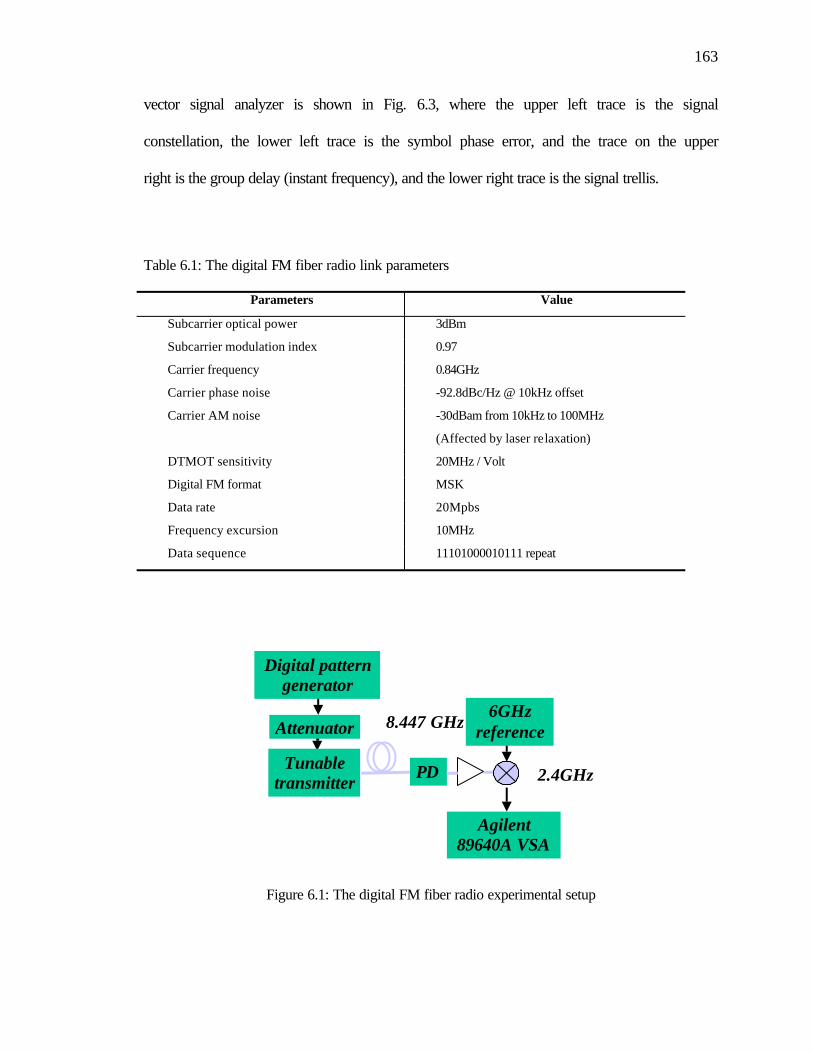
163
vector signal analyzer is shown in Fig. 6.3, where the upper left trace is the signal
constellation, the lower left trace is the symbol phase error, and the trace on the upper
right is the group delay (instant frequency), and the lower right trace is the signal trellis.
Table 6.1: The digital FM fiber radio link parameters
Parameters Value
Subcarrier optical power 3dBm
Subcarrier modulation index 0.97
Carrier frequency 0.84GHz
Carrier phase noise -92.8dBc/Hz @ 10kHz offset
Carrier AM noise -30dBam from 10kHz to 100MHz
(Affected by laser relaxation)
DTMOT sensitivity 20MHz / Volt
Digital FM format MSK
Data rate 20Mpbs
Frequency excursion 10MHz
Data sequence 11101000010111 repeat
PD
Attenuator
2.4GHz
Digital pattern generator
Tunable transmitter
6GHz reference
Agilent 89640A VSA
8.447 GHz
Figure 6.1: The digital FM fiber radio experimental setup

164
Figure 6.2: The fiber radio downlink noise charactistics
164

165
Figure 6.3: The demodulation result captured by the HP VSA
165

166
The MSK demodulation result looks very promising. The signal constellation and
trellis are decently clustered together. As shown in the signal constellation diagram,
however, the constellation points spread slightly in both tangential and radial directions.
They indicate the existence of the amplitude and phase errors in the fiber radio signal.
The amplitude error is caused by the laser relaxation oscillation and laser parasitic
amplitude modulation accompanied with the frequency modulation. The relaxation
oscillation is 30dB below signal level and should have only small effect. However, laser
parasitic AM can be significant because it will be resonantly enhanced close to the laser
relaxation frequency (1~5 MHz), which is within the MSK signal band. A sample of the
measured parasitic AM response is depicted in Fig. 6.4, where the Y axis unit is
Am/Volt. The dominant source of laser parasitic AM is the piezo effect of the LiNbO3,
which distorts the shape of the crystal and modulates the cavity loss when applying a
tunable voltage.
Figure 6.4: The parasitic AM response

167
The phase error shown in the signal constellation is due to ringing of the baseband
source. A sample of the baseband waveform is shown in Fig. 6.5.
Figure 6.5: The baseband signal ringing
In summary, a digital FM fiber radio transmission employing minimum shift
keying modulation was successfully demodulated. Except for the slight spread in the
signal constellation, the results are promising.
6.3 FM fiber radio up link and basestation implementation issues
The digital FM fiber radio system requires a different scheme for the basestation
implementation compared with the traditional fiber radio systems [7]. The basestation
scheme for the FM fiber radio system is shown in Fig. 6.6.

168
O/E conversion
MSK demodulator
Up link to center station
Down link from center station
Basestation
Laser Direct Modulation
VCO
PLL
LO
60GHz MSK signal
Figure 6.6: Fiber radio basestation
Inside the fiber radio basestation, the digital FM fiber radio signal is detected,
amplified and delivered to the mobile units via an antenna. A low cost baseband fiber link
is empolyed to implement the uplink communications from the basestation to the central
station. Inside the basestation, a LO at the mm-wave carrier frequency is required. For a
conventional fiber radio basestation, the LO signal could be genrated by injection locking
a local oscillator using the carrier signal from the downlink. However, if we employing
the digital FM scheme [57], no carrier tone can be identified in the downlink signal.
Therefore, only phase locking can be used to obtain the LO signal for the basestation of
the digtial FM fiber radio system.
6.5 Summary of fiber radio downlink testing
The digital FM fiber radio downlink transmission is demonstrated employing the
tunable mm-wave optic transmitter. Issues of the digital FM fiber radio downlink
maximum data rate are also addressed.

169
Chapter 7: Conclusions and recommendations for future work
In this chapter, a summary of thesis is presented and conclusions are drawn from
the theoretical and experimental results. In addition, recommendations for the future
work on tunable mm-wave optical transmitters are discussed.
7.1 Conclusions
The work in this thesis is concentrated on providing a low noise, rapidly tunable
mm-wave optical subcarrier source for hybrid lidar/radar, fiber radio and other
applications. Specifically, a rapidly tunable mm-wave optical transmitter using optical
heterodyning of two or more single mode electro-optically tunable microchip lasers has
been designed, implemented, and comprehensively evaluated. The transmitter can
generate a 20mW optical carrier with 100% mm-wave modulation index. The mm-wave
subcarrier frequency can be tuned from DC to over 100GHz. Limited by the driving
source, the tuning speed of the transmitter is at least 8.8GHz/µs.
The dynamics inside the tunable microchip laser are examined using the
Maxwell-Bloch equations. For the cases where the effective frequency tuning is much
less than the medium gain linewidth, we derived an approximate closed-form solution,
from which the decay time constants governing the laser transient response are
determined analytically.
The Maxwell-Bloch equations are later solved numerically by direct integration.
Extensive simulations have been performed to investigate the laser response for different
laser cavity parameters and voltage ramp rates. The laser has nearly unlimited tuning
speed. Due to the non-uniformity of the cavity, however, significant frequency ringing is

170
observed at very high tuning speeds. The ringing vanishes eventually and its decay time
agrees with the theoretical prediction.
In order to achieve low noise operation, two types of noise control subsystem are
studied, namely the digital synthesizer, and the optical frequency locked loop (OFLL).
The digital synthesizer is shown to be robust and easy to implement but its performance
degrades at higher frequencies. On contrast, the novel OFLL system has a performance
that is independent of the operation frequency. The conclusions drawn from the analytic
model of the OFLL indicate that:
• The OFLL phase noise performance is independent of the carrier
frequency
• The OFLL residual phase noise is lower with higher open loop gain
• The OFLL has a phase noise floor, which is a function of the system SNR
and the length of fiber delay
• Optimum delay time exists for a single loop OFLL in order to trade off the
noise floor and the residual phase noise. A multi-loop OFLL does not have
the above problem, and its residual phase noise and system noise floor can
be optimized independently.
The single loop OFLL employing a 90-meter delay is characterized at both lower
(<1.5GHz) and at higher frequencies (>20GHz). The measured phase noise at the lower
frequency is -108dBc/Hz at a 10kHz offset regardless of the operation frequencies, which
agrees with the theoretical expectation. At the higher frequency, however, the phase
noise measurement cannot be accurately performed due to the increased noise floor of the
measurement system. For a 38GHz carrier signal, the measurement yields a phase noise
171
of –97dBc/Hz at a 10kHz offset, which is the noise floor of the spectrum analyzer. The
actual phase noise at 38GHz should be lower.
Finally, the tunable transmitter is employed in a digital FM fiber radio downlink
transmission experiment with promising result. A 20Mbps MSK modulated fiber radio
signal at 8.4GHz is generated transmitted and successfully demodulated. The tunable
mm-wave optic transmitter is proved to be suitable for transmitting signal for a high
performance fiber radio downlink.
7.2 Recommendations for the future work
The results obtained in this thesis work encourage further research on the
microchip laser dynamics, tunable transmitter performance optimization, and a more in-
depth system level investigation of related applications. Specifically, the
recommendations for the future work are:
• Verifying experimentally the dynamic response of the laser under ramp
perturbation. As mentioned in Chapter 3, in order to observe significant frequency
ripples, the frequency tuning per round trip should be comparable to the cavity
FSR. However, it is very difficult to achieve experimentally using short cavity
microchip lasers. Therefore, a longer tunable laser may be preferred for
verification purposes. Then, the ripples can be recovered using optic domain
frequency/phase demodulation techniques such as delay homodyne, etc.
• Investigating the laser dynamic response under periodic perturbation close to the
cavity resonance frequency. Numeric simulation seems to point toward a more
complex dynamic behavior under high-speed periodic excitation including,
amplitude pulsing and chaotic behavior when the perturbation is close to the

172
cavity resonance frequency. A more detailed and rigorous theoretical study should
be undertaken to explore these phenomena.
• Improving the tunable microchip laser performance. First, the laser tuning
sensitivity needs to be increased by reducing the thickness of the electro-optic
section. Secondly, an improved pump system needs to be employed to improve
the transverse mode performance. Specifically, the spot size of the pump beam
must be reduced and it must be made more uniform. Thirdly, a tunable microchip
laser at 1.5 µm should be developed using Er:glass or other gain medium.
• A more sensitive phase noise measurement scheme. So far, we are unable to
determine the precise phase noise performance of the optical transmitter at higher
frequencies due to the limitation of the standard measuring apparatus. Therefore,
a better phase noise measurement scheme should be explored.
• Further decreasing the transmitter output phase noise. The analytical model shows
that the multi-loop OFLL has the potential of challenging the record level (-
150dBc/Hz @ 10kHz, 10GHz) of phase noise performance while maintaining the
advantage of broadband tunability from DC up to 100GHz. Therefore, the multi-
loop OFLL should be implemented experimentally to further decrease the
transmitter output phase noise.
• System level issues. The complete digital FM fiber radio system should be
examined, with emphasis on the suitable coding and modulation schemes, and the
architecture and implementation of low cost basestations. Multi-channel fiber
radio link should also be studied experimentally. Finally, the hybrid CWFM
lidar/radar needs to be investigated both theoretically and experimentally.

173
List of References
1. Mullen, L., et al., “Application of radar technology to aerial lidar systems for
enhancement of shallow underwater target detection”, IEEE Transactions on Microwave Theory and Techniques, Vol. 43, 9/2, , pp. 2370-2377, Sept. 1995.
2. Hughes A.J., et al., “FM-CW radar Range Measurement at 10 um Wavelength”, IEEE Journal of Quantum Electronics, Vol QE8, No. 12, pp. 909-910, Dec. 1972.
3. Honeycutt T.E., et al., “FM-CW radar Range Measurement with a CO2 Laser”, IEEE Journal of Quantum Electronics, pp. 91-92, Feb, 1972.
4. Schneider R., “Distance measurement of moving objects by frequency modulated laser radar”, Optical Engineering, Vol. 40, No. 1, pp. 33-37, January 2001.
5. Dieckmann, A., “FMCW-lidar with tunable twin-guide laser diode”, Electronics Letters, Vol. 30, No. 4, pp. 308-309, Feb. 17, 1994.
6. Li Y., et al., “Rapidly Tunable Millimeter-Wave Optical Transmitter for lidar/radar”, IEEE Transactions on Microwave Theory and Techniques, special issue on microwave and millimeter-wave photonics, Vol. 49, No. 10, pp. 2048-2054, Oct. 2001.
7. Ogawa H., et al., “Millimeter-wave Fiber Optics Systems for Personal Radio Communication”, IEEE Transactions on Microwave Theory and Techniques, Vol. 40, No. 12, pp 2285-2293, Dec. 1992.
8. A. Olsson et al., “Electrooptically tuned External cavity CW semiconductor Laser and FM optical Communications”, IEEE Journal of Quantum Electronics, Vol. QE-15, No. 10, pp. 1085-1088, October 1979.
9. Sato K., et al., “Fiber Optic Analog-Digital hybrid Signal Transmission Employing Frequency Modulation”, IEEE Transaction of Communications, Vol. COM-33, No. 5, pp. 433-441, May 1985.
10. Saito S., et al., “S/N and Error rate Evaluation for an Optical FSK-Heterodyne Detection System Using Semiconductor Lasers”, IEEE Journal of Quantum Electronics, Vol. QE-19, No. 2, pp.180-193, Feb. 1983.
11. Taylor R., et al., “Optically Coherent Direct Modulated FM Analog Link with Phase Noise Canceling Circuit”, Journal of Lightwave Tech., Vol. 17, No. 4, pp. 556-563, April 1999.
12. Gliese U., et al., “Multifunctional Fiber-Optic Microwave Links Based on Remote Heterodyne Detection”, IEEE Transactions on Microwave Theory and Techniques, Vol. 46, No. 5, pp. 458-468, May 1998.
174
13. Li Y., et al., “Generation of MSK Modulated Millimeter Wave Subcarrier for Radio Over Fiber Applications”, Proceedings of the Microwave Photonics 2001 Conference, Long Beach, CA, 2002, pp. 33-36, Jan. 7-9.
14. Zayhowski J.J., et al., Microchip lasers, Lincoln Lab. pp. 427, Jan. 1990.
15. Zayowski J.J., et al., “Single frequency microchip Nd:YAG lasers”, Opt. Lett. 24, 1989
16. MacKinnon, N., et al., “A laser diode array pumped Nd:YV4 /KTP, composite material microchip laser”, Opt. Communication. 105, pp. 183, 1994.
17. Matthews D.G., et al., “Blue microchip laser fabricated from Nd:YAG and KnbO3”, Opt. Lett. 21. pp. 198, 1996.
18. Zayhowski J.J., et al., “Diode pumped microchip lasers electro-optically Q switched at high pulse repetition rate”, Opt. Lett. 17, pp.1201, 1992.
19. Zayhowski J.J., et al., “Diode pumped passively Q switched picosecond microchip lasers”, Opt. Lett. 19, pp.1427, 1995.
20. Vieira A. J. C., et al., “Mode-Locked Microchip Laser Optical Transmitter for Fiber Radio”, IEEE Transactions on Microwave Theory and Techniques, special issue on microwave and millimeter-wave photonics, Vol. 49, No. 10, pp.1882-1887, Oct. 2001.
21. Zayhowski J.J., “The effects of spatial hole burning and energy diffusion on the single mode operation of standing wave lasers”, IEEE J. Quantum Electronics, 26, pp. 2052, 1990.
22. Kintz G. J., et al., “Single frequency operation in solid state laser materials with short absorption depths”, IEEE J. Quantum Electronics. 26, pp. 1457, 1990.
23. Zayhowski J.J., “Thermal guiding in microchip lasers”, OSA Proc. Advanced Solid State Lasers 6, Optical Society of America, Washington, DC, pp.9, 1991.
24. Gavrilvic P., et al., “Temperature tunable, single frequency microcavity lasers fabricated from flux grown YceAG:Nd, Appl. Phys. Lett. 60, pp. 1652, 1992.
25. Zayhowski J.J., “Frequency modulated Nd:YAG microchip laser”, Opt. Lett. 14, pp.618, 1989.
26. MacKinno N., et al., “Laser diode pumped, electro-optically tunable Nd:Mgo:LiNbO3 microchip laser, Journal of Optical Society of America, B11 (1994) pp 519
27. J.J Zayhowski,el al, “Diode pumped composite cavity electo-opticallly tuned microchip laser”, IEEE Photon Tech.. Lett. 5, pp.1153, 1993.
175
28. Schawlow A. L., et al., Phys. Rev. 112, pp.1940, 1958.
29. Yao, X.S., “Optoelectronic oscillator for photonic systems”, IEEE Journal of Quantum Electronics, Vol. 32, No. 7, pp.1141-1149, Jul, 1996.
30. Minakata, M, “Recent progress of 40 GHz high-speed LiNbO3 optical modulator”, Proceedings of SPIE - The International Society for Optical Engineering, Vol. 4532, pp.16-27, 2001.
31. Yariv A., IEEE 52, 719, 1964
32. Genack A.Z., et al., “Optical coherent transients by laser frequency switching”, Physics Review A, Vol. 17, No. 14, pp 1463-1473, April 1978
33. Harris S.E., et al., Applied Physics Letter, 5, pp.205, 1964
34. Harris S.E., et al., Applied Physics Letter, 5, pp.202, 1964
35. Harris S.E., “Theory of FM Laser Oscillation”, IEEE Journal of Quantum Electronics, Vol. QE-1, No.6, pp.245-262, Sep. 1965.
36. Kuizenga D.J., et al., IEEE J. Quantum Electronics, QE-6, pp.694, 1970.
37. Longhi S., et al., “Time-domain analysis of frequency modulated laser oscillation”, APL, Vol. 73, No. 6, pp.720-725, Aug. 10, 1998.
38. Haus H.A., et al., “A Theory of Forced Mode Locking”, IEEE Journal. of Quantum Electronics, Vol. QE11, No. 7, pp.323-329, July 1975.
39. Lamb W.E., Jr., “Theory of an optical Maser,” Phys. Rev., Vol. 134, pp. A1429-A1450, Jun. 1964.
40. Abraham N.B., “Dynamic instability and pulsations in Lasers”, Progress in Optics XXV, pp.1-189, edited by E. Wolf, 1988
41. Longhi S., et al., “Floquet theory of intracavity laser frequency modulation”, Physical Review A, Vol. 60, No. 50, pp. 4016-4027, Nov. 1999
42. Casix Inc., category, 2001
43. Shen Y. R., "The Principles of Nonlinear Optics", ISBN: 0-471-88998-9,May 1984
44. Lugiato L.A., et al., “Multimode instabilities in a homogeneously broadened ring laser”, Physical Review A, Vol. 32, No. 3, Sep. 1985.
45. Siegman A., “Lasers”, Mill Valley, Calif. University Science Books, c1986

176
46. Edwards, C. H., “Differential equations and boundary value problems: computing and modeling”, Upper Saddle River, N.J: Prentice Hall, c2000.
47. Koechner, W., “Solid State Laser Engineering”, Berlin, New York: Springer, c1996.
48. Vieira A.J.C., "Optical transmitter with Millimeter-wave subcarrier", Ph.D. Thesis, Drexel University, Philadelphia, PA, 1997.
49. VLOC, Product catalog, pp 60. VLOC, 7826 Photonics Drive, New Port Richey, FL 34655 U.S.A.
50. Zayhawski J.J., et al., "Frequency tuning of Microchip lasers using pump power modulation", IEEE Journal of Quantum Electronics, Vol. 28, No. 4, pp.1118 – 1122, April 1992.
51. Ni T. D., et al., "Experimental Study on Close-In to Microwave Carrier Phase Noise of Laser Diode with External feedback", IEEE transactions on Microwave Theory and Techniques, Vol. 43, No. 9, pp.2277 – 2282, Sep. 1995.
52. Egan, W. F., “Frequency synthesizing by phase locking”, 2nd edition, New York : John Wiley, c2000.
53. Pozar D.M., “Microwave engineering”, New York: Wiley, [1997], c1998
54. Silvano D., “Photodetectors : devices, circuits, and applications”, Upper Saddle River, N.J. : Prentice Hall PTR, c2000.
55. Yao, X. S., et al., “ Multiloop optoelectronic oscillator”, IEEE Journal of Quantum Electronics, Vol. 36, No. 1, pp.79-84, Jan. 2000.
56. Chen C.T., “Introduction to Linear System”, New York: Holt, Rinehart, and Winston, c1984.
57. Proakis J.G., “Digital Communication”, Boston : McGraw-Hill, c2001.

177
Appendix A. The closed-form solution of electro-optic section
The objective of the appendix is to derive the closed-form functional mapping
between the optical field at arbitrary location and the input boundary under electro-optic
perturbation. The propagation equation (Eq. 3.6) for the dimensionless field envelope
inside the E/O section is a first-order partial differential equation for which a closed-form
solution exists. To facilitate the solution, the E/O tuning section is depicts separately in in
figure A.1.
V(t)
LiNbO 3 Dielectric
Z Z=z2
Z=z3
Figure A.1: A separate E/O tuning section
First we introduce the space coordinate transform to unify the dimensions of the
space and time coordinate.
czzz /)(~2−= (A.1)
where c is the speed of light. Then, z~ has the dimension of time.
Under the new space coordinate, equation 3.6 has the form,
Ω⋅⋅⋅⋅=∂Ω∂
+∂Ω∂ ~
)(2~
~~332
0
0 tEdn
izt tuning
ω (A.2)
To solve equation A.2, we rotate the ( zt ~, ) coordinates using,

178
ztvztu~
;~
−=+=
(A.3a)
2/)(~2/)(
vuzvut
−=+=
(A.3b)
z-z2
t u
v
The field envelope in the t-axis is given by boundary condition
The field envelope on the z-axis is given by initial condition
(t,z)
(t,z)
Legend: Line of direct integration
Figure A.2: Coordinate transform from ( z~ ,t) plane to (u,v) plane
In (u,v) coordinates, equation A.2 takes the form,
2
22332
0
0 Ω⋅
+
⋅⋅
=∂Ω∂
vuEd
ni
u
tuningω
(A.4)
Expressing the envelope in terms of a phase and an amplitude, φ⋅=Ω iAe , equation A.4
reduces to:
0=∂∂
uA
(A.5a)
2
22332
0
0
+
⋅⋅
=∂∂
vuEr
nu
tuningω
φ (A.5b)

179
Furthermore, equation A.5 yield,
)()~()( 2
czz
tAztAvAA−
−=−== (A.6a)
and,
),(2
22),( 0
3320
0
0
vudu
vuEr
nvu
u
u
tuning
φ
ω
φ +
+
⋅⋅
= ∫ (A.6b)
In equation A.6b, the integration is along the constant v line (figure A.2) in the
(u,v) plane. If we use 2/)( vut += as the integration variable, then equation A.4b
becomes,
),()(2
),( 0
2/)(
2/)(3320
0
0
vudttErn
vuvu
vu tuning φω
φ +⋅⋅= ∫+
+ (A.7)
The phase, ),( vuφ is to be determined by initial or boundary condition depending
where they are located in the (u,v) plane( figure A.2).
As shown in figure A.2, when, v<0, i.e., czzzt /)(~2−=< , ),( vuφ is obtained by
the initial condition. For the initial time instant t=0, equation. A.1b yields vu −=0 , while
equation A.3a yields, ztv ~−= , then equation. A.7 gives the phase change in the
),( zt coordinate,
)0,()(2
),( 203320
=−−+⋅⋅⋅= ∫ tctzzdttErn
tzt
tuning φω
φ (A.8)
In contrast, when, v>0, i.e., czzzt /)(~2−=> , ),( 0 vuφ is obtained by the
boundary condition. At the boundary 2zz = , equation A.1b yields vu =0 , while equation
A.3a yields ztv ~−= , then equation A.7 gives the phase change in the (z,t) plane,

180
),()(2
),( 22
/)( 3320
2 czz
tzzdttErn
tzt
czzt tuning
−−=+⋅⋅⋅= ∫ −−
φω
φ (A.9)
Initially, for t<0 there is no tuning voltage and the electro-optic section behaves
like an ideal delay element. Therefore, when t=0, the optical envelope can be obtained
from the field envelope at the time t<0. That is,
)/,0(~)0,(~ cztztz −=Ω==Ω
Applying the above constraint into equation A.8, we find that equation A.8 and
A.9 can be presented together just by equation. A.7 alone.
Using the complex field envelope, equations A.6a and A.9 can be expressed more
concisely as,
∫ ⋅⋅⋅ −−⋅−−=Ω==Ωt
czzt tuning dttEieczztzztzz
/)2( )(
22 )/)(,(~
),(~ β
(A.10)
where 3320
0
2d
n⋅=
ωβ
The closed-form mapping between the complex field envelope at arbitrary
location and the start of electro-optic section is revealed in equation A.8, which states that
the effect of electro-optic element introduces a constant time delay and phase change.
The phase change is depends on the history of the applied tuning field. When the tuning
field is slow varying compared with the propagation time, it is reduced to the form for the
lumped electro-optic modulator.

181
Appendix B. Simulation method based on the direct integration of Maxwell-Bloch equation
Maxwell-Bloch equation Eq. 3.20 can be solved numerically by direct two-
dimensional integration as has been done previously by Narducci L.M., et al.. However,
their numeric approach is based on the 2nd order Taylor expansion method, which
depends on the exact form of the partial differential equation (P.D.E.). Complicated
calculations have to be performance beforehand to obtain the simulation parameters in
order to start the numeric integration. In addition, those parameters often depend on the
derivative of the perturbation term (i.e., tG ∂∂ / for our case), which does not always
have an explicit form. Worst of all, this calculation has to be performed each time the
dynamic equation changes due to inclusion of different perturbation signal. In this
appendix, we are going to derive new direct integration method suitable for solving the
Maxwell-Bloch equation system under external perturbation.
B.1 Maxwell-Bloch equations system in the discrete form
As the first step, we obtain the discrete form of the Maxwell-Bloch equations.
Without the loss of generality, the Maxwell-Bloch equation is represented in the form
used by Narducci [40], et al.,
)2('
FCPkzF
tF
n
+−=′∂
∂+
∂∂
(B.1.a)
ptzfipidFtp
AC ⋅⋅−+−=′∂
∂⊥ )','(])
~1(.[ δγ (B.1b)
]1)/ln'2exp()[(21 ** ++⋅⋅−⋅+⋅−=
′∂∂
dLRzpFpFtd
Cγ (B.1c)

182
where 2C is the constant describing the gain coefficient, and b)/c(1z'z n +⋅= is the
normalized space variable. Equation B.1 and 3.20 are equivalent except that they differ in
the interpretation of polarization and steady state inversion density.
The equations for the envelope of the polarization and the inversion density are in
the O.D.E. form and the difficulty of the direct numeric solution comes from equation
B.1a. To make it easier, we write 3.61a in the gradient form.
)2(2
)( 0 FCPk
eF +−=⋅∇rr
(B.2)
where, n
zt ze
te
n ′∂∂
+′∂
∂=∇ ′′
rrr, )(
21
0 nzt eee ′′ +=rrr
, and te ′r
, 'nz
er
is the unity vector in t’ and
z’ direction respectively. From the Field theory, we obtain,
ldFtzFtzFzt
zt
rr∫ •∇=−
),(
),(0000
00
)','()','( (B.3)
If both points (z’,t’) and (z0’, t0’) lie in the same path parallel with the vector 0er
, equation
B.3 is reduced to the ordinary integratal form, i.e.,
dlFCPk
tzFtzFztzt
⋅+−=− ∫>− )','(),(
00
00
)2(2
)','()','( (B.4)
If
htthzz
+=+=
''''
0
0
where h is a small step size.
Then, Eq. B.4 yields,
duFCPktzFhthzFh
∫ ⋅+⋅−=−++00000 )2()','()','( (B.5)
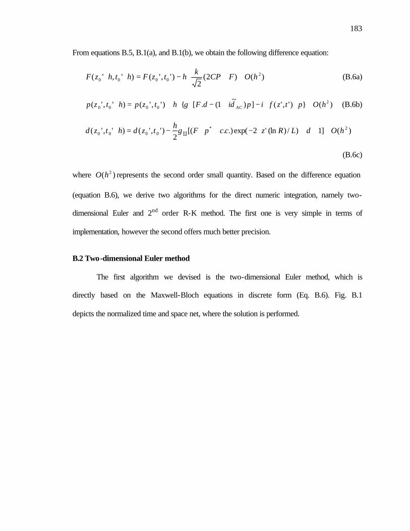
183
From equations B.5, B.1(a), and B.1(b), we obtain the following difference equation:
)()2(2
)','()','( 20000 hOFCP
khtzFhthzF ++⋅−=++ (B.6a)
)()','(])~
1(.[)','()','( 20000 hOptzfipidFhtzphtzp AC +⋅⋅−+−⋅+=+ ⊥ δγ (B.6b)
)(]1)/)(ln'2exp(.).[(2
)','()','( 2*0000 hOdLRzccpF
htzdhtzd +++⋅⋅−+⋅−=+ Cγ
(B.6c)
where )( 2hO represents the second order small quantity. Based on the difference equation
(equation B.6), we derive two algorithms for the direct numeric integration, namely two-
dimensional Euler and 2nd order R-K method. The first one is very simple in terms of
implementation, however the second offers much better precision.
B.2 Two-dimensional Euler method
The first algorithm we devised is the two-dimensional Euler method, which is
directly based on the Maxwell-Bloch equations in discrete form (Eq. B.6). Fig. B.1
depicts the normalized time and space net, where the solution is performed.

184
z’=0 z’=L’
t’
h
h
(zm’, t n’) (zm+1’, tn’)
(zm’, tn+1’) (zm+1’, tn+1’)
Figure B.1: Normalized time and space net to carry out the solution process.
By truncating the higher order small quantities (O(h2) terms), we immediately get
the difference equation for the Euler method,
)2(, ,,,11 nmnmnmnm FCPkhFF +⋅⋅−=++ (B.7a)
)],('
[])~
1(.[ ,,,,,1, nmnmnmACnmnmnmnm PtztG
iPidFhPP ⋅∂∂
⋅−+−⋅+= ⊥+ δγ (B.7b)
]1)/)'*(ln*2exp(.).[(2 ,
*,,,1, ++−+⋅−=+ nmmnmnmnmnm dLRzCCPF
hdd Cγ (B.7c)
With boundary condition,
1,10 , ++ = nMn FF (B.7d)
where h is the simulation step, m is the subscript for the space variable and
m=0,1,2,… (M-1), M is the total number of space point considered; and n is subscript for
the time coordinate variable, n =0,1,2 … The program flow diagram for the two
dimensional Euler method is shown in Fig. B.2.

185
Start
Enter initial condition: Fm,0 Pm,0 dm,0
Get (F,P,d)m,n+1 from (F,P,d)m,n using eq 3.68, m=0,1,2,… M-1
Enough time duration
End
n++
No
Figure B.2: The flow diagram for two-dimension Euler method.
The two dimension Euler method is a first order approach since the single step
error it introduced is: O(h2). For this reason, Euler method is a first order method with a
low precision, and it is not very suitable for the simulation of the instantaneous
frequency.
B.3 Two-dimensional Runge-Kutta method
In order to simulating the instantaneous optical frequency, we devised a numeric
method with higher precision, namely the two-dimensional Runge-Kutta method, which
we are going to explain in detail.
The starting point of Runge-Kutta (R-K) method is the single step estimation of
Euler method (Eq. B.7). To simplify the algorithm description, we use the following
notation,
)2(),,,','(1 FCPkdpFztf +−= (B.8a)

186
PtzfiPidFdPFztf AC ⋅⋅−+−= ⊥ )','(])~
1(.[),,,','(2 δγ (B.8b)
]1)/)(ln'2exp()[(21
),,,','( **3 ++⋅⋅−⋅+⋅−= dLRzpFpFdPFztf Cγ (B.8c)
The time-space net as shown in Fig. B.1 is also employed to perform the two
dimensional Runge-Kutta numeric solution. For simplicity, we only consider the second
order method. Higher order Runge-Kutta (>2) method can be derived in a similar fashion.
In the following, we’ll explain the single step estimation of the 2nd order R-K method in
detail, namely identifying the field, polarization, and inversion density (F,P,d)m,n at the
time instance t=tn= hn × , from the previous values of (F,P,d)m,n-1, m=0,1,2,…, M-1.
Step 1.
Using single step Euler estimation, we calculate the intermediate value,
1,)ˆ,ˆ,ˆ( +nmdPF , m=0, 1,2,… M-1, i.e.,
),,,(,ˆ,,,1,11 nmnmnmnmnmnm dPFtzfhFF ⋅⋅+=++ (B.9a)
),,,,(ˆ,,,2,1, nmnmnmnmnmnm dPFtzfhPP ⋅+=+ (B.9b)
),,,,(ˆ,,,3,1, nmnmnmnmnmnm dPFtzfhdd ⋅+=+ (B.9c)
With the boundary condition
1,10 ,ˆ++ = nMn FF
) (B.9d)
Step 2.
Using middle point theorem, we estimate field, polarization, and inversion density
values at the middle points, i.e., 2/1,)ˆ,ˆ,ˆ( +nmdPF , m=0, ½,1, 3/2, … M-1, M-1+1/2. The
middle points are marked as the blue diamonds in Fig. B.1.
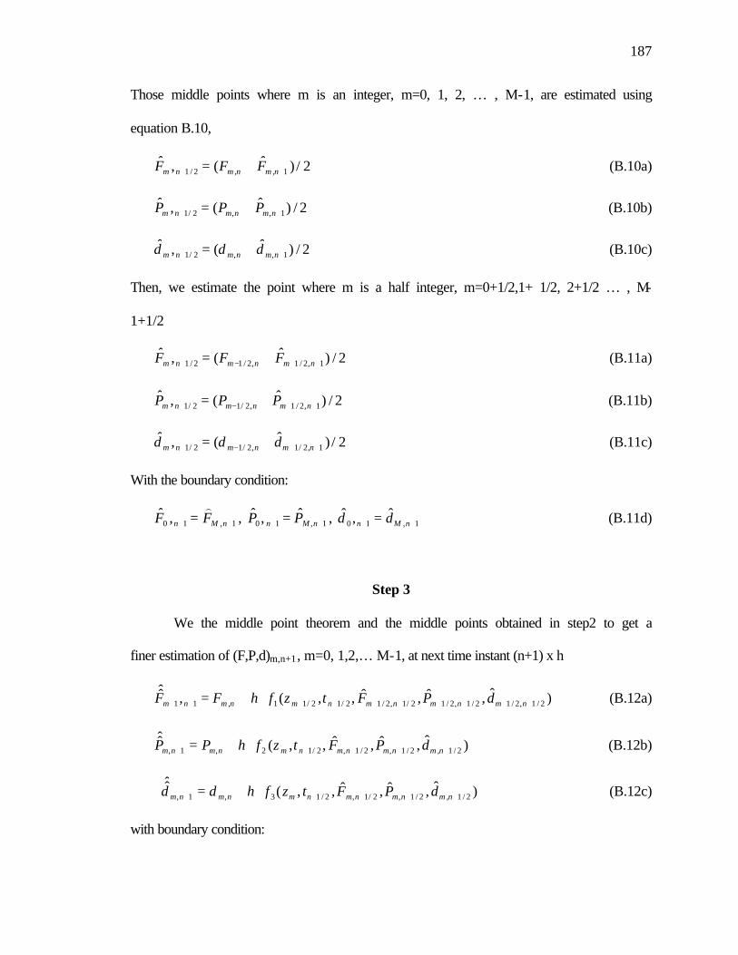
187
Those middle points where m is an integer, m=0, 1, 2, … , M-1, are estimated using
equation B.10,
2/)ˆ(,ˆ1,,2/1 ++ += nmnmnm FFF (B.10a)
2/)ˆ(,ˆ1,,2/1 ++ += nmnmnm PPP (B.10b)
2/)ˆ(,ˆ1,,2/1 ++ += nmnmnm ddd (B.10c)
Then, we estimate the point where m is a half integer, m=0+1/2,1+ 1/2, 2+1/2 … , M-
1+1/2
2/)ˆ(,ˆ1,2/1,2/12/1 ++−+ += nmnmnm FFF (B.11a)
2/)ˆ(,ˆ1,2/1,2/12/1 ++−+ += nmnmnm PPP (B.11b)
2/)ˆ(,ˆ1,2/1,2/12/1 ++−+ += nmnmnm ddd (B.11c)
With the boundary condition:
1,10 ,ˆ++ = nMn FF
), 1,10
ˆ,ˆ++ = nMn PP , 1,10
ˆ,ˆ++ = nMn dd (B.11d)
Step 3
We the middle point theorem and the middle points obtained in step2 to get a
finer estimation of (F,P,d)m,n+1, m=0, 1,2,… M-1, at next time instant (n+1) x h
)ˆ,ˆ,ˆ,,(,ˆ2/1,2/12/1,2/12/1,2/12/12/11,11 ++++++++++ ⋅+= nmnmnmnmnmnm dPFtzfhFF (B.12a)
)ˆ,ˆ,ˆ,,(ˆ2/1,2/1,2/1,2/12,1, +++++ ⋅+= nmnmnmnmnmnm dPFtzfhPP (B.12b)
)ˆ,ˆ,ˆ,,(ˆ
2/1,2/1,2/1,2/13,1, +++++ ⋅+= nmnmnmnmnmnm dPFtzfhdd (B.12c)
with boundary condition:
188
1,10ˆ,ˆ
++ = nMn FF)
(B.12d)
At this stage, we obtains the signal step estimation of (F,P,d)m,n+1 for the second
order two dimension R-K method. The single step error of this method is O(h3), and
therefore, it is a second order method. It should be emphasized that just by following the
steps similar to the traditional Runge-Kutta method, the higher order two-dimensional
method could be implemented as well. The flow diagram for the second order R-K
method is shown in Fig. B.3.
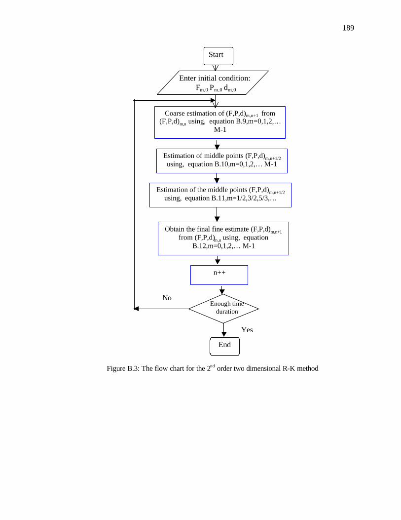
189
Start
Enter initial condition: Fm,0 Pm,0 dm,0
Coarse estimation of (F,P,d)m,n+1 from (F,P,d)m,n using, equation B.9,m=0,1,2,…
M-1
Enough time duration
End
n++
No
Estimation of middle points (F,P,d)m,n+1/2 using, equation B.10,m=0,1,2,… M-1
Estimation of the middle points (F,P,d)m,n+1/2 using, equation B.11,m=1/2,3/2,5/3,…
Obtain the final fine estimate (F,P,d)m,n+1 from (F,P,d)m,n using, equation
B.12,m=0,1,2,… M-1
Yes
Figure B.3: The flow chart for the 2nd order two dimensional R-K method

190
Appendix C. The derivation for fundamental mode cross section
In this appendix, we derive the closed-form expression specifically for the
fundamental mode cross section of the tunable laser cavity. First, the temperature field
inside the tunable laser is determined. Then the mode cross section is obtained using a
self-consistent condition for the transverse profile of the lasing field.
C.1 Temperature field inside the E/O tunable microchip laser crystal The E/O tunable microchip spatial mode is defined by the pump beam thermal
effect. Therefore, as the first step, we solve for the pump beam induced temperature field
inside the E/O microchip laser crystal. We assume that pump adsorption only occurs
inside the gain section and heat dissipates transversely inside the gain section. In
addition, for simplicity, it is also assumed that the E/O section maintains constant
temperature and its thermal guiding effect is neglected. The temperature field inside the
cavity satisfies the Laplace equation,
ckRP
T)(2
r⋅
−=∇α
(C.1)
where, α is the heat-generating efficiency of the pump, Rr
is three dimensional space
vector, P( Rr
) is the absorbed pump power distribution over space, and kc is the thermal
conductivity.
If the fundamental mode cross-section is much smaller than crystal cross-section,
the temperature field inside the modal volume should have cylindrical symmetry.
Therefore, Eq. C.1 can be greatly simplified in the cylindrical coordinates as,

191
ckrP
rT
rrT )(12
2 ⋅−=
∂∂
+∂∂ α
(C.2)
where r is the radius from the center of the cylinder.
Inside the modal volume, the temperature field can be expanded in a Taylor
series,
...)( 33
2210 +⋅+⋅+⋅+= rTrTrTTrT (C.3)
Substituting Eq. C.3 into Eq. C.2, we can get
....
9)0(
4)0(
,0
4
3
2
1
=
′⋅−=
⋅−=
=
T
kP
T
kP
T
T
c
c
α
α
(C.4)
To simplify the derivation, we neglect the 3rd or higher order effect. As a result,
the temperature field becomes,
20 4
)0()( r
kP
TrTc
⋅⋅
−=α
(C.5)
where T0 is determined from the crystal boundary condition. Next we calculate the spatial
mode cross-section.
C.2. Fundamental spatial mode cross-section Due to the transverse variation of temperature field (Eq. C.5), the refractive index
inside the Nd:YVO4 gain section varies quadratically from the optical axis. In addition,
the dielectric mirror deposited on the Nd:YVO4 surface will be deformed parabolically

192
by thermal expansion along the optical axis. The combined effect is equivalent to
introducing a change in the optical path,
)()()()( rTlrTlnlnl effne ⋅⋅=⋅+⋅= αααδ (C.6)
where n is the refractive index of Nd:YVO4, l is the Nd:YVO4 length, eα and nα are
Nd:YVO4 thermal expansion coefficient and refractive index temperature coefficient
respectively, and neeff n ααα +⋅= .
In case of the E/O tunable microchip laser, the gain section (with thermal effect)
is much shorter than overall cavity length. Therefore, we use the conceptual model
depicted in Fig. C.1 to study the thermal guiding effecting,
duct
lducf<<Leff
Leff
M1 M2 Ef
Eb
Figure C.1: The conceptual cavity structure under thermal guiding effect
In Fig. C.1, Leff is the effective cavity length,
LTlnLL effeff ≈⋅⋅⋅+= 0α
where L is the initial cavity length; ductl is the length of the infinitesimal thin duct inside
the conceptual cavity, 2
4)0(
rkP
llc
effduct ⋅⋅
⋅−=α
α

193
The negative length of duct is used to model the thermal effect, which introduces
a negative parabolic phase delay to the optical field inside the cavity,
2/4
)0( 22 rkrkP
lklkc
effductdelay ⋅∆⋅−=⋅⋅
⋅−=⋅=α
αφ (C.7a)
where
ceff k
Pl
2)0(⋅
⋅=∆α
α (C.7b)
λπ /2=k is the wave number in the vacuum (C.7c)
Under para-axial approximation, the fundamental optical field is a complex
Gaussian,
))(2
exp()(
1),(
2
zqr
kjnzq
zrE⋅
⋅−= (C.8)
where q(z) is the q-parameter of complex Gaussian wave. Next, we use a self-consistent
approach to calculate the fundamental spatial modal field.
Let 0q denote the q parameter of the Gaussian wave at beginning of the duct,
fq and bq are the q parameters of the forward and backward Gaussian waves at the end of
the duct respectively. Then 0q , fq and bq satisfy the following three equations,
nqq f
∆−=0
11 (C.9a)
efffb Lqq 2+= (C.9b)
nqq b
∆−=11
0
(C.9c)

194
where Eqs. C.9aa and C.9c result from parabolic phase change inside the duct and Eq.
C>(b follows from free space propagation model of complex Gaussian wave. Solving Eq
C.9, we get,
2)(1
nLeffnj
nq f
∆−
⋅∆
−∆
−= (C.10)
Substituting Eq. C.10 into Eq. C.8, we obtain the Gaussian beam waist at the gain
section,
knnLeffn
⋅⋅
∆−
⋅∆
=2
])([
1
412
ω (C.11)
Using the condition for the weak thermal guiding, i.e., n
Leff∆
>>/1 , the express
for the fundamental mode cross section (Eq. C.11) is reduced to:
knLeffn
⋅⋅
⋅∆
≈2
][
1
41
ω (C.12)
Substituting Eqs C.7b and C.7c into Eq. C.12, we obtain the final result for the
fundamental mode cross section as a function of the pump and laser cavity parameters,
4/1
4/1
)()
2
)0((
1l
L
nnk
Peff
c
eff
⋅⋅
⋅
⋅
⋅⋅≈
πλ
ααω (C.13)

195
Appendix D. A new discriminator structure minimizing the AM to phase noise conversion
The OFLL conceptual diagram (see Fig. 5.2) is over simplistic in terms of
practical implementation. The non-ideally balanced mixer introduces a subcarrier AM
noise into the frequency discriminator output, and significantly raises the OFLL phase
noise floor. In this section, we’ll discuss the OFLL implementation scheme (see in Fig.
5.4) that suppresses subcarrierr AM to PM noise conversion.
In Fig. 5.4, the mm-wave carrier signal of the second (delayed) path is amplitude
modulated by a fixed low frequency signal (fm) using mixer (double sideband up-
converter) M1, whose output is later mixed with the mm-wave carrier signal from the
first path by the second mixer M2, and the M2 output signal is mixed with the low
frequency modulation signal to recover the subcarrier phase error information (Eq. 5.8).
Next, we prove that using this approach, the subcarrier AM noise to phase noise
conversion is greatly suppressed.
The mixer M1 output signal is given by,
))(cos())(1(
)cos())(cos())(1()(
02/
0211
τφωτ
ωτφωτ
−+−++
−+−+=
tttnAk
ttttnAAktIF
IFRF
mmm (D.1)
The mixer M2 output signal is given by,
)cos())()(sin())()(1()( 021212 ttttntnAAAkktIF mnnmmm ωτωτφφτ +−−⋅−++=
)cos())(21(22/12 ttnAAkkk mmIFRFmb ωτ ⋅−+⋅+ (D.2)
The mixer M3 output signal is,
))()(sin()( 02
213213 τωτφφ +−−⋅= ttAAAkkktIF nnmmmm
))(21(222/312 τ−+⋅+ tnAAkkkk mIFRFmmb (D.3)

196
where kRF/IF is the RF / IF isolation of the first mixer, km1, km2 , km3 are the constants
related to the conversion gains of three mixers respectively, kb2 is the constant describing
the degree of balance of the second mixer. In the derivation, the second order terms (i.e.,
cross product between the AM and PM noise, etc) and signal components outside the
system bandwidth are neglected.
In the output (Eq. D.3) of the improved OFLL discriminator, the first term on the
RHS represents the phase error, while the second term describes the subcarrier AM to
phase noise contribution. In order to quantitatively analyze the AM to phase noise
conversion, we need to calculate the AM noise conversion to phase error ratio (APR) at
the discriminator output,
))()(sin())(2(
012
2/2
τωτφφτ+−−⋅
−⋅⋅==
ttAktnAkk
errorPhaseconversionnoiseAM
APRnnm
IFRFb (D.4)
The APR of the improved discriminator depends strongly on,
• The AM modulation index of first mixer (i.e., 2
// mIFRF kk ),
• The balance of second mixer and
• The ratio between the amplitudes of the first and second path
If the mixer balance remains the same, the subcarrier AM noise to phase noise
conversion is suppressed by the following expression,
dB )/log(20)log(20nSuppressio 21 AAIndex AM += (D.5)

197
Vita
Yifei Li was born in Anqin, Anhui province, P. R. of China, on March 30, 1974.
He received a B.S. degree in Electrical Engineering at Huazhong University of Science
and technology, Wuhan, P.R. China. He received an M. S. degree in Electrical
Engineering at Drexel University in Philadelphia, Pennsylvania in June 2001.

198


![Optically tunable and detectable magnetoelectric effects ...web.phys.ntu.edu.tw/nanomagnetism/eng/pdf/086... · devices [8,9], laser diodes [8–10] ranging from infrared to ultraviolet](https://img.pdfslide.net/doc/110x75/5f88a3d44d20e621e342bd08/optically-tunable-and-detectable-magnetoelectric-effects-webphysntuedutwnanomagnetismengpdf086.jpg)