Embed Size (px)
Citation preview

General rights Copyright and moral rights for the publications made accessible in the public portal are retained by the authors and/or other copyright owners and it is a condition of accessing publications that users recognise and abide by the legal requirements associated with these rights.
• Users may download and print one copy of any publication from the public portal for the purpose of private study or research. • You may not further distribute the material or use it for any profit-making activity or commercial gain • You may freely distribute the URL identifying the publication in the public portal
If you believe that this document breaches copyright please contact us providing details, and we will remove access to the work immediately and investigate your claim.
Downloaded from orbit.dtu.dk on: May 28, 2018
Optimal Design and Tradeoffs Analysis for Planar Transformer in High Power DC-DCConverters
Ouyang, Ziwei; Thomsen, Ole Cornelius; Andersen, Michael A. E.
Published in:The 2010 International Power Electronics Conference - ECCE ASIA - IPEC-Sapporo 2010
Publication date:2010
Document VersionPublisher's PDF, also known as Version of record
Link back to DTU Orbit
Citation (APA):Ouyang, Z., Thomsen, O. C., & Andersen, M. A. E. (2010). Optimal Design and Tradeoffs Analysis for PlanarTransformer in High Power DC-DC Converters. In The 2010 International Power Electronics Conference - ECCEASIA - IPEC-Sapporo 2010 IEEE.

Copyright (c) 2010 IEEE. Personal use is permitted. For any other purposes, Permission must be obtained from the IEEE by emailing [email protected].
This article has been accepted for publication in a future issue of this journal, but has not been fully edited. Content may change prior to final publication.
Optimal Design and Tradeoffs Analysis of Planar Transformer in High Power DC-DC Converters
Ziwei Ouyang, Student Member, IEEE, Ole C. Thomsen Member, IEEE and Michael A. E. Andersen Member, IEEE
Abstract -- The trend toward high power density, high
operating frequency, and low profile in power converters has exposed a number of limitations in the use of conventional wire-wound magnetic component structures. A planar magnetic is a low profile transformer or inductor utilizing planar windings instead of the traditional windings made of Cu-wires. In this paper, the most important factors for planar transformer (PT) design including winding loss, core loss, leakage inductance and stray capacitance have been investigated individually. The tradeoffs among these factors have to be analyzed in order to achieve optimal parameters. Combined with an application, four typical winding arrangements have been compared to illustrate each their advantages and disadvantages. An improved interleaving structure with optimal behaviors is proposed, which constructs the top layer paralleling with the bottom layer and then in series with the other turns of the primary so that a lower magneto motive force (MMF) ratio m can be obtained as well as minimized AC resistance, leakage inductance and even stray capacitance. A 1.2-kW full-bridge DC-DC converter prototype employing the improved planar transformer structure has been constructed, over 96% efficiency is achieved and a 2.7% improvement compared to the non-interleaving structure is obtained.
Index Terms-- planar transformer, interleaving, winding loss, core loss, leakage inductance, stray capacitance, magneto motive force (MMF), finite element analysis (FEA), DC-DC converter.
I. INTRODUCTION HE trend toward high power density, high operating frequency, and low profile in power converters has
exposed a number of limitations in the use of conventional wire-wound magnetic component structures. In recent years, planar transformer (PT) has become increasingly popular in high-frequency power converters because of the unique advantages they achieved in terms of low profile, excellent thermal characteristic, modularity and manufacturing simplicity, increased reliability and power density [1]-[3]. The use of higher switching frequency can result in passive component size reduction, which achieves higher power density in power converter. However, as well as for the conventional magnetic structures, the demand of high-frequency operation also causes a number of limitations in planar magnetic structures, such as the problem of increased losses due to the skin and the proximity effects particularly at
frequencies above 100 kHz. Regarding winding AC resistance, many efforts have been made to derive expressions allowing for an accurate representation of frequency behavior of AC resistance. The AC resistance effects due to high frequency current are tailored specifically for transformers by Dowell [4]. This work is based on a one dimensional solution of the diffusion equation as applied to conducting parallel plates. The expression for AC resistance has been rearranged in [5] due to the squared porosity factor η. The comparison of various methods for calculating the AC resistance of windings is given in [6]. The papers [7]-[9] analyze and improve the AC resistance expression specifically for different situations. Based on Dowell’s equation, an optimum layer-thickness of conductors minimizing winding loss can be found, which also affects the leakage inductance significantly as shown in paper [20]. Regarding core loss, there are three main methods to calculate: hysteresis models [11]-[12], loss separation approach [13], and empirical methods. Empirical approach enables loss determination with manufacturer provided data with an easy way to use expression. The typical expression, the Steinmetz equation, is limited by some constraints so that many publications focus on improving Steinmetz equation to extend its use [14]-[19].
In this work, a detail analysis in winding loss, core loss, leakage inductance and stray capacitance has been presented. The tradeoffs among these factors have to be analyzed in order to achieve an optimal design. Furthermore, winding arrangements can in part bring an optimal behavior in the tradeoffs without any sacrifices, which play an important role in optimizing PT. Combining with an application in 1.2-kW full-bridge DC-DC converter, four different winding arrangements have been compared to illustrate each their merits and drawbacks. An improved interleaving structure 0.5P-S-P-S-P-S-P-S-0.5P is proposed, which constructs the top layer paralleling with the bottom layer and then in series with the other turns of the primary so that a lower MMF ratio m can be obtained as well as minimized AC resistance, leakage inductance and even stray capacitance. The detail experimental results have been shown in section IV.
II. DETAIL DESIGN CONSIDERATION
A. Winding Loss Winding losses in transformers increase dramatically with
high frequency due to eddy current effects. For design and optimization of transformers, there is a need for an accurate prediction of the winding losses over a wide frequency range and for various winding arrangements. Eddy current losses,
T
Manuscript received November 27, 2009. Accepted for publication January 25, 2010. This work is supported by Flux A/S. Copyright © 2009 IEEE. Personal use of this material is permitted. However, permission to use this material for any other purposes must be obtained from the IEEE by sending a request to [email protected] The authors are with the Department of Electrical Engineering, Technical University of Denmark, 2800 Kongens Lyngby, Denmark (e-mail: [email protected]; [email protected]; [email protected]).
Authorized licensed use limited to: Danmarks Tekniske Informationscenter. Downloaded on July 27,2010 at 14:22:48 UTC from IEEE Xplore. Restrictions apply.

Copyright (c) 2010 IEEE. Personal use is permitted. For any other purposes, Permission must be obtained from the IEEE by emailing [email protected].
This article has been accepted for publication in a future issue of this journal, but has not been fully edited. Content may change prior to final publication.
including skin effect and proximity effect losses seriously impair the performance of transformers in high-frequency power conversion applications. For AC current flowing in a conductor, the alternating field inside this conductor induces eddy currents in the conductor which produce a field that tends to cancel the field produced by the original current. The tendency of the alternating current distributes itself within the conductor so that the current density near the surface of the conductor is greater than that at its center. This is called skin effect which causes the effective resistance of the conductor to increase with the frequency of the current. The proximity effect is similar but it is caused by the current carried by an adjacent conductor. The current in the adjacent conductor causes a time-varying field and induces a circulating current inside the conductor. Both the skin effect and the proximity effect cause the current density to be non-uniform in the cross-section of the conductor and thus cause a higher winding resistance at higher frequency.
The skin effect of an infinite foil conductor with sinusoidal excitation can be represented by the ratio of AC resistance to DC resistance as in [9]:
ξξξξξ
coscoshsinsinh
2 −+
⋅=dc
ac
RR (1)
where ξ=h/δ, and δ is skin depth in the conductor.
Based on Dowell’s assumptions and the general field solutions for the distribution of current density in a single layer of an infinitely foil conductor, the expression for AC resistance of the mth layer is derived as [5], [9].
⎥⎦
⎤⎢⎣
⎡+−
⋅−+−+
=ξξξξ
ξξξξξ
coscoshsinsinh)12(
coscoshsinsinh
22
,
, mRR
mdc
mac (2)
where m is defined as a ratio in (3),
)0()()(FhF
hFm−
= (3)
where F(0) and F(h) are MMFs at the limits of a layer as shown in Fig. 1. The first term in (2) is identical to (1) which describes the skin effect. And the second term represents the proximity effect factor. The proximity effect loss, in a multilayer winding, may strongly dominate over the skin effect loss depending on the value of m which is related to the winding arrangement. Interleaving transformer windings can reduce the proximity loss significantly when the primary and secondary currents are in phase. Fig. 1(a) and (b) show the MMF distributions alone vertical direction for non-interleaving arrangement and fully interleaving arrangement respectively. The value of m can be calculated according to (3) and quite different results are shown in Fig. 1 as well. In order to further illustrate the eddy current effect in different arrangements, a finite element analysis (FEA) tool
is used to analyze current distribution inside the conductors. Fig. 2 and Fig. 3 individually represent current distributions for interleaving windings and non-interleaving windings when the excitation frequency is 50 kHz. A two-dimensional PT model with cylindrical symmetry about Z axis has been built and all of conditions are the same in both figures except winding arrangement. It can be seen from the two figures that current density is higher towards the symmetrical Z-axis due to the DC spirality effect. The skin and the proximity effects can further increase the non-uniform distribution of current density when the frequency goes high. In other words, the color division of current distribution is not only caused by the DC spirality effect, but also by the skin and the proximity effects. It is noteworthy that AC resistance will not be contributed by the DC spirality effect. For the non-interleaving arrangement in Fig. 3, the tendency of current density toward conductor surface is enhanced due to higher proximity effect. The strongest tendency toward conductor surface appears in the layer close to the interface between the primary and the secondary, and thus the area of color division becomes smaller which means a higher AC resistance will be produced.
As seen in (2), AC resistance is not only related to MMF ratio m, but also dependent on the ratio ξ. With a given frequency, the minimal AC resistance can be determined by the layer-thickness of windings. The choice of thickness as a physical parameter has been a key in optimizing PT. Fig. 4 shows that the ratio of AC resistance to DC resistance increases with increasing thickness at a fixed frequency. For a large m, the proximity effect dominates over the skin effect which leads to a higher winding resistance. With decreasing thickness of the conductor, the ratio is close to 1 which represents a low eddy current effect in the conductor, but the DC resistance will be increased. Hereby, minimal AC resistances can be figured out for different MMF ratios m as shown in Fig. 5. Regarding the case that several number of turns are involved in a layer, the proximity effect among them in horizontal direction can be almost negligible if the
Fig. 1. MMF distributions. (a) Non-interleaving arrangement, and (b) Interleaving arrangement.
Authorized licensed use limited to: Danmarks Tekniske Informationscenter. Downloaded on July 27,2010 at 14:22:48 UTC from IEEE Xplore. Restrictions apply.

Copyright (c) 2010 IEEE. Personal use is permitted. For any other purposes, Permission must be obtained from the IEEE by emailing [email protected].
This article has been accepted for publication in a future issue of this journal, but has not been fully edited. Content may change prior to final publication.
width is much more than the thickness, otherwise the porosity factor η needs to be introduced [5], [9]. As seen in Fig. 5, the MMF ratio m is referred to be as small as possible so that a minimal AC resistance can be obtained. In fact, it is not practical in the middle frequency because a relative thicker conductor needs to be used. The window space of core is also a limitation on this issue. However, in high-frequency application (above 500 kHz), the MMF ratio m of 0.5 can be implemented practically because of very small skin depth.
Parallel connection of multi-layer for planar winding is now usually employed to increase the current handling capacity of the winding. However, with parallel winding connections, the magnetic field around windings becomes more complicated. Due to the leakage fluxes and the high frequency effects, the currents may not be equally shared among the paralleled layers. In other words, circulating currents may exist in parallel layers, which contributes to an extra winding loss. The papers [1] and [10] present the extra winding loss caused by “parallel effect loss” (circulating currents) in detail.
There are many limitations on the validity of (2) such as minimum distances between consecutive turns, between adjacent layers, and between the conductor edge and the magnetic core, as well as sinusoidal waveform. The most outstanding work as a calculation method of AC resistance for any current waveform to correct Dowell’s assumptions
can be found in [8]. And also several publications get generalized correction factors to be applied in Dowell’s resistance factor expression. However, these factors are usually derived from elaborated formulas and have to be determined from complicated coefficient tables [9]. Outside these minimum boundaries, it is advisable to determine winding losses with FEA simulations.
B. Core Loss Referring to most of the literature, there are three main
methods to deal with magnetic loss: hysteresis models, loss separation approach, and empirical methods. The former is usually based on Jiles-Atherton or Preisach models [11], [12]. The loss separation approach assumes that three fundamental effects are contributing to core losses: static hysteresis loss, eddy current loss and excess eddy current loss [13]. Finally, the empirical approaches are based on the Steinmetz equation, a curve-fitting expression of measured data under sinusoidal excitation. Although the hysteresis models and loss separation
Fig. 2. Current distribution in fully interleaving arrangement.
Fig. 3. Current distribution in non-interleaving arrangement.
10-1
100
10110
0
101
102
m=0.5
m=1
m=2
m=3m=4
m=5
m=6
m=7
m=10
h
dc
ac
RR
Fig. 4. The ratio of AC resistance to DC resistance as a function of ξ and MMF ratio m.
100
101
100
101
102
m=1
m=0.5
m=2
m=3
m=4m=5m=6m=7m=10
1dc
ac
R
R
h10
-1
10-1
Fig. 5. AC resistance relative to DC resistance in a layer having effective thickness of skin depth.
Authorized licensed use limited to: Danmarks Tekniske Informationscenter. Downloaded on July 27,2010 at 14:22:48 UTC from IEEE Xplore. Restrictions apply.

Copyright (c) 2010 IEEE. Personal use is permitted. For any other purposes, Permission must be obtained from the IEEE by emailing [email protected].
This article has been accepted for publication in a future issue of this journal, but has not been fully edited. Content may change prior to final publication.
approach can lead to satisfactory results, require extensive computations and measurement works. Empirical approach enables loss determination with manufacturer provided data with an easy way to use expression.
Nowadays, Steinmetz equation is widely used in the design of magnetic components in power converters, which expresses core loss density as power law with fixed exponent of frequency and flux density,
βα )2/( BfKPv Δ⋅⋅= (4)
where K, α, β are constants provided by manufacturer, ΔB is the peak to peak flux density which can be obtained from Faraday’s law,
eANtVB
⋅Δ⋅
=Δ (5)
where N is the number of turns, Ae is the cross-section of the core and V·Δt means volt-seconds.
However, (4) is only valid for sinusoidal waveform and in some case, loss for non-sinusoidal waveform can far exceed the loss due to sinusoidal ones, even when the frequencies and the peak flux densities are both equal. The paper [19] has been proven that core loss can lead to an error up to 45% in relation to the measured results for an H-bridge converter case operates with square waveform with zero-voltage period. In order to deal with any waveforms, some modified expressions including modified Steinmetz expression (MSE) [14], generalized Steinmetz equation (GSE) [15], improved GSE (IGSE) [16], natural Steinmetz extension (NSE) [17], equivalent elliptical loop (EEL) [18] and waveform coefficient Steinmetz equation (WCSE) [19] were introduced. A complete comparison among these modified empirical methods for bidirectional isolation DC-DC converter shows the MSE and the IGSE have the best loss determination; however, the IGSE copes better with a wide variety of voltage waveform [19].
dtBdt
tdBkT
PT
iv ⋅Δ⋅⋅= −∫ αβα
)()(10
∫ ⋅⋅⋅=
−− π αβαα θθπ2
0
1 2cos)2( d
Kk i . (6)
K, α, β are determined by equating the loss expression for a sinusoidal excitation case with (4). The angle θ represents the phase angle of the sinusoidal waveform. Applying a piecewise linear model (PWL) to the non-sinusoidal waveform and then combining it with the IGSE, leads to an easy-to-use expression for the determination of core loss. Furthermore, it is believed that the IGSE is the most practical method for calculating core loss with non-sinusoidal
waveforms in most high-frequency magnetics design work, because it requires only readily available sinusoidal loss data, in the form of parameters for the Steinmetz equation characterizing the material. For the full-bridge DC-DC converter operates with the symmetrical square waveforms, a new extension of Steinmetz equation can be deduced based on the IGSE and the PWL model,
1122 +−− ⋅⋅⋅⋅= αββαα DBfKP sqmv (7)
where D is the switching duty cycle. Bsqm is the peak flux density when the square waveform is with 50% duty cycle, which can be obtained from (5), Bsqm= (V·T) / (4N·Ae).
According (7), core loss can be determined by number of turns, core cross-section, excitation voltage, duty cycle, core volume and material. The peak flux is inversely proportional with the frequency, and the exponent β is higher than the exponent α in general magnetic materials. Therefore, core loss will decrease with increasing frequency. The frequency leads to a tradeoff between winding loss and core loss because high frequency increases AC resistance significantly as presented before. With increasing number of turns, core loss can be benefit from the lower peak flux density but sacrificing winding loss. Using several cores to be cascade to increase the core cross-section can minimize the flux density, but it also increases winding loss because an extra length of winding is added.
C. Leakage Inductance Not all the magnetic flux generated by AC current
excitation on the primary side follows the magnetic circuit and link with the secondary winding. The flux linkage between two windings or parts of the same winding is never complete. Some flux leaks from the core and returns to the air, winding layers and insulator layers, thus these flux causes imperfect coupling.
The energy associated with leakage inductance can be calculated according to analyze MMF distribution and energy distribution. From the Fig. 1, the differential volume of each turn is lw·bw·dx, therefore the total energy is sum of the energy stored in each elementary layer which can be given by
∑ ∫ ⋅⋅⋅=h
wwlk dxblHE0
20
2μ (8)
where lw is the length of each turn, bw is the width of each turn, h represents the thickness of each winding layer. The thickness dx, situated at a distance x from the inner surface of conductor. The field strength H depends on the number of ampere turns linked by the leak flux path. Since the flux disperses rapidly on leaving the winding, the associated energy is much reduced and the reluctance of the path within magnetic core can be ignored compared with that of the path
Authorized licensed use limited to: Danmarks Tekniske Informationscenter. Downloaded on July 27,2010 at 14:22:48 UTC from IEEE Xplore. Restrictions apply.

Copyright (c) 2010 IEEE. Personal use is permitted. For any other purposes, Permission must be obtained from the IEEE by emailing [email protected].
This article has been accepted for publication in a future issue of this journal, but has not been fully edited. Content may change prior to final publication.
in the windings, herby the flux path can be expressed by the width bw rather than the full closed flux path [20], [21]. According to (8), for non-interleaving structure in Fig. 1(a), the leak energy in total winding space can be deduced then,
⎥⎥⎥⎥⎥⎥⎥⎥
⎦
⎤
⎢⎢⎢⎢⎢⎢⎢⎢
⎣
⎡
⋅+
++⋅+++⋅+
∫ ∫ ++⋅+⋅⋅+⋅⋅
⋅⋅=
Δ
ΔΔ
Δ
hbI
hhhbIhhh
bI
hhhbIdxh
xbIdxh
xbI
blE
w
ww
h h
www
wwlk
21
2121
2121
10
20 21
212
2
12
1
1
0
)4(
)2()3()2()2(
)2()()(4)(4
2μ
2210 443
)(462 p
w
wlk Ihhh
bl
E ⋅⎥⎦
⎤⎢⎣
⎡ ++
⋅= Δμ (9)
where h1 and h2 are the lay-thickness of the primary and the secondary respectively, hΔ is the height of insulator layer. However, as for fully interleaving arrangement in Fig. 1(b), with the same approach, leakage inductance can be deduced as follows,
⎥⎦⎤
⎢⎣⎡ +
+⋅⋅= Δhhh
blL
w
wleakage 3
4 210μ . (10)
Apparently, the fully interleaving arrangement provides a
significant advantage in reducing leakage inductance. As a conclusion, besides winding structures, leakage inductance in PT can be changed by adjusting some physical parameters including conductor thickness and its width, insulator thickness and number of turns. As a parasitic element exists in transformers, the leakage inductance causes the main switch current at the device input to vary at a low slope between zero and rated value and reduces the rate of commutation between output diodes. In addition, the stored energy in the leakage inductance leads to a generation of voltage spikes on the main switch which, besides creating EMI problems, increases the switching losses and lowers the efficiency. However, in some applications such as a phase-shift-modulated soft switching DC/DC converter, the magnitude of leakage inductance determines the achievable load range under ZVS operation, and a relatively large leakage inductance is desirable. In order to avoid an additional magnetic component, a leakage layer with low permeability has been inserted between the primary and the secondary, to form a resonant inductor [22].
D. Stray Capacitance Stray capacitance in designing PT can’t be ignored. The
potential between turns, between winding layers and between windings and core create this parasitic element. In most papers about optimizing PT, the main purpose is to reduce leakage inductances, but stray capacitances have not seriously been considered. In fact, stray capacitances significantly affect the magnetic component performance in
such a way that the current waveform on the excitation side would be distorted and the overall efficiency of converters would be decreased. Subjected to high voltage stresses, stray capacitance between windings causes leakage currents and consequently contributes EMI problem [25].
Considering an equivalent model of two-winding PT as shown in Fig. 6, where Rp and Rs are the resistances of the primary and secondary windings. Cpo, Cso and Cpso are used to account for the self-capacitances of the primary and the secondary windings and the mutual capacitance between the two windings, respectively. It is desirable to keep Cpso to be as small as possible, and good EMI results could be achieved. The equivalent capacitors referred to the primary side can be determined approximately by the following relations [26],
psopop CkCC ⋅−+= )1(
psosos CkkCkC ⋅−⋅−⋅= )1(2
spstr CCC +≈ (11)
where k is the turns ratio. The mutual capacitance Cpso due to the electrical coupling between the primary and the secondary windings can be approximately measured directly by shorting both primary and secondary sides. The single equivalent capacitance referred to the primary side, Cstr in Fig. 7 can be approximately computed by (11).
In the case of PTs, static layer capacitances can be estimated easily since the windings consist of parallel and flat conductors. The formula for the capacitance between two parallel conductive plates is given by,
Δ⋅⋅=
hSC r 00 εε (12)
where εo is the permittivity of free air space, εr is the relative permittivity of the material. And S represents the overlapping
N1:N2
LIkRp
Cpo Lm Cso
Rs
Cpso
N1:N2
LIkRp
Cstr Lm
Rs
(a)
(b)Fig. 6. Equivalent circuit of transformer model (a) with self-capacitances and mutual capacitance, and (b) with single lumped stray capacitance referred to the primary side.
Authorized licensed use limited to: Danmarks Tekniske Informationscenter. Downloaded on July 27,2010 at 14:22:48 UTC from IEEE Xplore. Restrictions apply.

Copyright (c) 2010 IEEE. Personal use is permitted. For any other purposes, Permission must be obtained from the IEEE by emailing [email protected].
This article has been accepted for publication in a future issue of this journal, but has not been fully edited. Content may change prior to final publication.
surface area of the two plates. The distance between the plates is hΔ. Fig. 7(a) shows equivalent potential distribution model in dependence on the internal two layers of the same winding with opposite direction. Assuming that the potential distribution along the turns varies linearly,
Un
inUi ⋅−+
=)1( (i=1,2,3….,n) (13)
where n is number of turns in each layer and Ui represents the potential in each pair of plates. U is the voltage potential between the two terminations of the winding. The turn-to-turn capacitance C1 can be ignored by comparing with the layer-to-layer capacitance C0 due to very small overlapping surface area. The total energy associated with electric field in the two layers is given by,
20
2
1
20
1 12)12)(1(1
21 UC
nnn
ninUCEE
n
i
n
ii
++=⎟
⎠⎞
⎜⎝⎛ −+
== ∑∑==
. (14)
The equivalent capacitance of the same winding can be expressed by:
02 6)12)(1(2 C
nnn
UECd
++== . (15)
If there is m layers in series for the same winding as the same connection as Fig. 7(a), the overall equivalent capacitance could be deduced by equating the electric energy stored in all layers capacitors [29],
dd CmmC 2
' )1(4 −= . (16)
For the connection in Fig. 7(b), that provides an equivalent constant voltage distribution along the turns in each layer. Hereby, a lower equivalent capacitance Cd=(n/4)·Co in the winding with same direction has been shown up. Regarding stray capacitance in different windings, the voltage difference between high potential side and low potential side can be expressed by UΔ=UH-UL as shown in Fig. 7(c). The assumption that linear distributed voltage along different windings is still in valid. With the same procedure, the equivalent stray capacitance referred to the primary winding can be deduced by
02
22
2)1(6)12(
2 CU
UnUUnnnnU
UEC
LL
w
ΔΔ +−−
+== . (17)
Based on the above analysis for the stray capacitance, the
optimal solutions can be concluded as follows; 1) Reducing static layer capacitance by enhancing the distance or lowering the overlapping surface area between the two conductor
plates; 2) Reducing number of turns in each layer or/and increasing number of layers; 3) Reducing number of intersections between the primary and the secondary; 4) Arranging winding configurations to obtain the minimal energy associated with the electric field.
III. TRADEOFFS ANALYSIS Combining with the analysis of winding loss, core loss,
leakage inductance and stray capacitance, some overlapping occur in affecting each other as follows,
1) The number of turns N. The less N can bring less winding loss, but more core loss will be produced due to higher peak flux density; furthermore a lower leakage inductance also can be obtained. The stray capacitance is also probably benefited depending on the winding configuration. The choice of N will have to be a key in optimizing design.
2) The excitation frequency f. Although a higher frequency can cause a lower core loss as mentioned before, AC resistance will be increased due to eddy current effect. The leakage inductance slightly decreases with increased frequency because of a small change in the permeability of conductors. The designed frequency has to be considered the carrying capacity of switching devices as well as the switching losses.
3) The thickness of conductors h and insulator hΔ. The optimal thickness h for winding loss has been introduced in section II. A larger h also causes a larger leakage inductance. There is a contradiction for hΔ between the leakage inductance and the stray capacitance. The larger hΔ, the larger leakage inductance and the smaller capacitance. It is impossible to achieve both low values by optimizing the physical parameters. The only way to obtain optimal behaviors both leakage inductance and stray capacitance is to change winding configurations. Considering the loss in
U +
_C0 C0 C0U1 U2 Un
C1 C1
C1 C1
UL
+
_C0 C0 C0U1 U2 Un
C1 C1
C1 C1
UH
+
_
(a)
(c)
U +
_C0 C0 C0U1 U2 Un
C1 C1
C1 C1
(b)
Fig. 7. Equivalent potential distribution model in dependence on (a) the internal two layers of the same winding with opposite direction; (b) the internal two layers of the same winding with same direction; (c) the two layers of the different windings.
Authorized licensed use limited to: Danmarks Tekniske Informationscenter. Downloaded on July 27,2010 at 14:22:48 UTC from IEEE Xplore. Restrictions apply.

Copyright (c) 2010 IEEE. Personal use is permitted. For any other purposes, Permission must be obtained from the IEEE by emailing [email protected].
This article has been accepted for publication in a future issue of this journal, but has not been fully edited. Content may change prior to final publication.
parasitic elements, a low leakage inductance has priority over a low stray capacitance in high-current low-voltage application. Reversely, in low-current high-voltage application a low stray capacitance has to be required rather than a low leakage inductance.
4) The core geometry. For a certain number of turns, a bigger cross-section Ae of core can bring a lower core loss, but the length of windings will have to be sacrificed which increases winding loss.
In order to facilitate a clear understanding of tradeoffs in PT design, a 1:1 turn ratio transformer will be analyzed as an example for simplification. The assumed specification of a full-bridge buck DC-DC converter with primary excitation 50V/20A, duty cycle 50% and switching frequency 50 kHz is used. Fully interleaving is employed to form that the MMF ratios m in each layer is equal to 1. According to the analysis of winding loss and Fig. 5, 0.25mm thickness of conductors is chosen in this example. The authors write a small programme in virtue of Matlab to figure out the tradeoffs. Fig.8 shows the total loss, the winding loss and the core loss vary as a function of different number of turns when the other parameters are fixed. The red curve and blue curve individually represent the total loss for E-I-58 core and E-I-64 core. The core losses decrease with the increased number of turns this is due to the fact that the flux density is reduced. The winding losses, however, increase due to higher DC resistances are achieved. Apparently, an optimal number of turns in this example can be found. And Fig. 9 reflects a relationship between losses and frequency. An optimal frequency for the total loss can be found as well. Taken together Fig. 8 and Fig. 9, the intersection points between red line and blue line illuminates the tradeoff also caused by the core geometry.
Following the analysis of AC resistance and core loss, the relationship between the losses and number of turns N can be written by,
NKPw ⋅= 1
β−⋅= NKP c 2
⎥⎦
⎤⎢⎣
⎡+−
+−+
⋅⋅⋅=ξξξξ
ξξξξξ
coscoshsinsinh
coscoshsinsinh
22 2
1 dcRIK
1122 )
4(2 +−− ⋅
⋅⋅⋅⋅⋅= αββαα D
AfVfKK
e
(18)
The total loss is,
β−⋅+⋅= NKNKPt 21 (19)
The minimum of (19) is achieved by taking the partial derivative N, and setting to zero:
0121 =⋅⋅−=
∂∂ −− ββ NKK
NPt (20)
The optimal number of turns N,
1
21
KKN ⋅
=+ ββ (21)
cowo PP ⋅= β (22)
The minimum loss occurs when the winding loss is β times the core loss. The Fig. 8 also proves the place where the minimum loss occurs.
IV. EXPERIMENTAL COMPARISON Winding arrangements also can in part bring an optimal
behavior in the tradeoffs without any sacrifices, which play an important role in optimizing PT. In the following work, four typical winding arrangements are compared to illustrate each their advantages and disadvantages. Fig. 10 individually
Loss
es (W
)
Fig. 8. Total loss, winding loss and core loss vary with different number of turns in comparison of two planar cores.
Loss
es(W
)
Fig. 9. Total loss, winding loss and core loss vary with different frequency incomparison of two planar cores.
Authorized licensed use limited to: Danmarks Tekniske Informationscenter. Downloaded on July 27,2010 at 14:22:48 UTC from IEEE Xplore. Restrictions apply.

Copyright (c) 2010 IEEE. Personal use is permitted. For any other purposes, Permission must be obtained from the IEEE by emailing [email protected].
This article has been accepted for publication in a future issue of this journal, but has not been fully edited. Content may change prior to final publication.
shows their 3-D models. A full-bridge buck DC-DC converter employing these PTs has been built with the specifications presented in Table I.
TABLE I
SPECIFICATIONS OF TRANSFORMER Parameters Values Input voltage 50 V Input current 20 A
Turns ratio (N2/N1) 2:1 (8:4) Core type EELP 64
Core material Ferrite N87 Operating frequency 50 kHz
Duty cycle 50% Cross-section of core 519 mm2
Volume of core 41500 mm3 Thickness of copper foil
(primary) 0.25 mm
Thickness of PCB winding (secondary)
70 um * 4 (4 layers in parallel)
Insulator 0.1mm Kapton Tape
TABLE II MEASUREMENT RESULTS OF PARASITIC PARAMETERS
Frequency is 50 kHz Rac/Rdc (mOhm)
Lleak
(nH)
Cstr (nF)
Non-interleaving 32.2/6.55 324 1.15 P-S-P-S-P-S-P-S 9.14/6.14 43.8 9.41 P-S-S-P-P-S-S-P 10.1/6.21 47.4 4.24 P/2-S-P-S-P-S-P-S-P/2 7.68/5.69 40.6 3.89
Model a:
Non-interleaving has very high AC resistance and leakage inductance comparing with other arrangements as shown in Fig. 11 and Fig. 12. However, it merits the stray capacitance because of only one intersection between the primary and the secondary. Table ІІ shows the lowest stray capacitance can be achieved in the non-interleaving arrangement. Model b:
Based on Table ІІ, Fig. 11 and Fig. 12, AC resistance and
leakage inductance are reduced dramatically in general full interleaving P-S-P-S-P-S-P-S. A lower MMF ratio m causes a weaker proximity effect in the adjacent layers, which contributes a lower AC resistance. The energy associated with leakage inductance is reduced this is due to the fact that the magnetizing force is reduced in each layer as shown in Fig. 1(b). However, seven intersections between the primary and the secondary can be found where a higher stray capacitance caused by. As shown in Table ІІ, the stray capacitance in P-S-P-S-P-S-P-S is almost 10 times than that in non-interleaving. Model c:
P-S-S-P-P-S-S-P is another kind of full interleaving arrangement because the MMF ratios m in each layer are still equal to 1 as shown in Fig. 13(a). Comparing with the general full interleaving P-S-P-S-P-S-P-S, it has similar AC resistance and leakage inductance because their MMF distributions have the same functions. However, it is very noteworthy that stray capacitance is getting better without sacrificing any other behaviors (leakage inductance or AC resistance) this is due to the fact that fewer intersections (four) between the primary and the secondary can be found. Model d:
Model d represents an improved interleaving arrangement which constructs the top layer paralleling with the bottom layer and then in series with the other turns of the primary so that the MMF ratio m can be reduced further. Fig. 13(b) shows the analytical MMF distribution of 0.5P-S-P-S-P-S-P-S-0.5P. Since an unavoidable error of impedances on top and bottom layers, the currents in each branch are probably not equal and hence the MMF ratios m may not be 0.5. Anyhow, a lower MMF ratio m below 1 can be achieved. Thereby, as shown in Fig.11, a lower AC resistance appears in high frequency situation and a slow increasing tendency can be clearly identified when the frequency is above 100 kHz. The most impressive thing is not only AC resistance and leakage inductance can be reduced, but also stray capacitance can be benefit compared with the other interleaving arrangements. The paper [32] proposed that quadruple interleaving also achieves m=0.5 by splitting the secondary. However, the even turn ratio is limited in this construction as well as the stray capacitance might not be improved.
Fig.10 3-D models (a) non-interleaving (b) P-S-P-S-P-S-P-S (c) P-S-S-P-P-S-S-P (d) improved interleaving 0.5P-S-P-S-P-S-P-S-0.5P
Authorized licensed use limited to: Danmarks Tekniske Informationscenter. Downloaded on July 27,2010 at 14:22:48 UTC from IEEE Xplore. Restrictions apply.

Copyright (c) 2010 IEEE. Personal use is permitted. For any other purposes, Permission must be obtained from the IEEE by emailing [email protected].
This article has been accepted for publication in a future issue of this journal, but has not been fully edited. Content may change prior to final publication.
Fig.14 shows measured impedance with opening secondary winding in P-P-P-P-S-S-S-S, P-S-P-S-P-S-P-S, P-S-S-P-P-S- S-P and 0.5P-S-P-S-P-S-P-S-0.5P arrangements respectively. The non-interleaving has best parallel LC resonance frequency (L=magnetizing inductance; C=stray capacitance of primary) and the worst case occurs in the full interleaving P-S-P-S-P-S-P-S. Due to the magnetizing inductance in the four arrangements are the same, the parallel
LC resonance frequencies reflect the magnitude of the stray capacitors as the same results as shown in Table II.
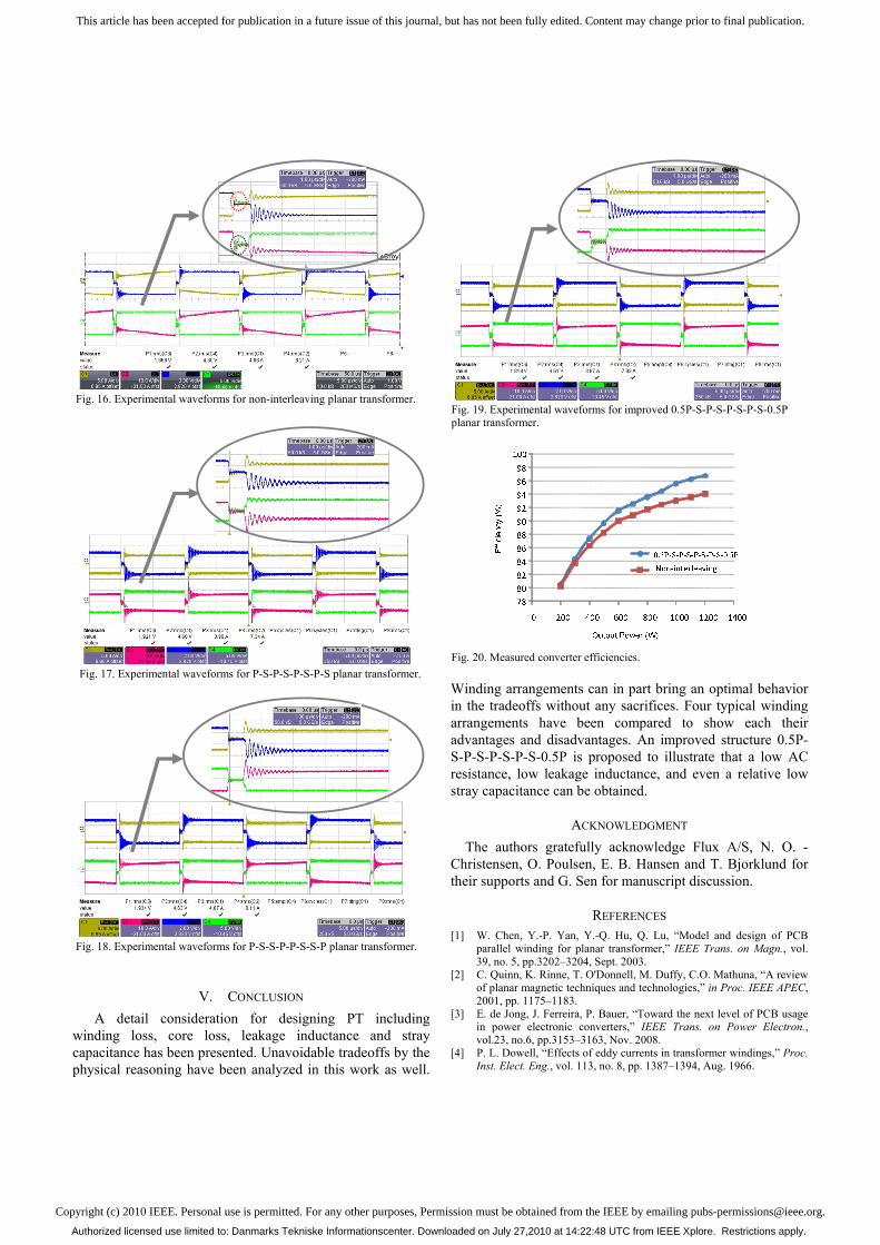
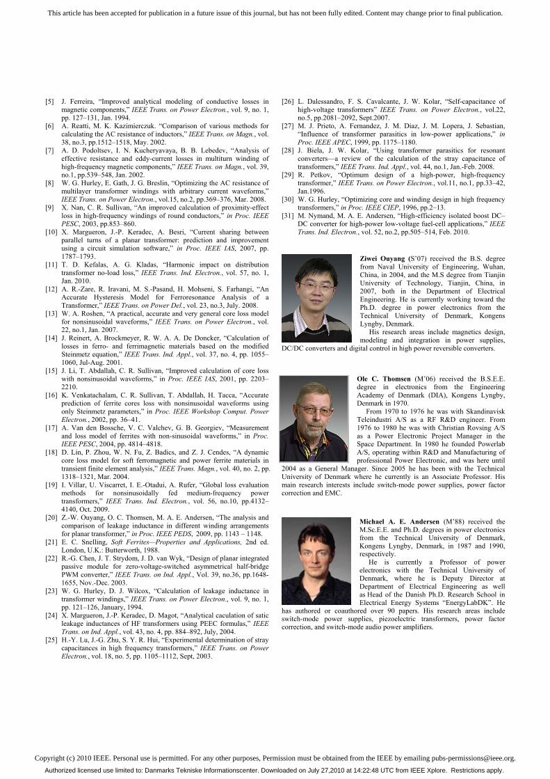
A 1.2-kW full-bridge converter prototype employing the improved planar transformer structure has been constructed as shown in Fig. 15. Fig. 16-19 shows the plots of transformer primary voltage, primary winding current, secondary voltage and current in different winding arrangements. In these figures, C3 and C4 represent the voltage across the transformer secondary winding and primary winding respectively. C1 and C2 represent the current on transformer primary and secondary respectively. A bigger ringing spike occurs in the dead time (or zero-voltage length if the duty cycle is not 0.5) for the non-interleaving arrangement this is due to the fact that the energy stored in the leakage inductance oscillates with the other parasitic elements in the circuit. The improved 0.5P-S-P-S-P-S-P-S-0.5P arrangement has the best high frequency property in ringing problem which can bring low switching losses and low EMI problem. The measured converter efficiencies are shown in Fig. 20. Over 96% efficiency can be achieved for the improved transformer and a 2.7% improvement compared to the non-interleaving structure is obtained when the output power is 1.2-kW.
Fig. 14. Measured impedance with opening secondary winding in P-P-P-P-S-S-S-S, P-S-P-S-P-S-P-S, P-S-S-P-P-S-S-P and 0.5P-S-P-S-P-S-P-S-0.5P respectively.
Rac
(Ohm
)
Fig. 11. AC resistances measurement.
Leak
age
Indu
ctan
ce (H
)
Fig. 12. Leakage inductances measurement.
Fig. 13. MMF distributions for (a) P-S-S-P-P-S-S-P and (b) 0.5P-S-P-S-P-S-P-S-0.5P respectively.
Fig. 15. Photo of 1.2-kW full bridge DC-DC prototype employing animproved PT.
Authorized licensed use limited to: Danmarks Tekniske Informationscenter. Downloaded on July 27,2010 at 14:22:48 UTC from IEEE Xplore. Restrictions apply.
Copyright (c) 2010 IEEE. Personal use is permitted. For any other purposes, Permission must be obtained from the IEEE by emailing [email protected].
This article has been accepted for publication in a future issue of this journal, but has not been fully edited. Content may change prior to final publication.
V. CONCLUSION A detail consideration for designing PT including
winding loss, core loss, leakage inductance and stray capacitance has been presented. Unavoidable tradeoffs by the physical reasoning have been analyzed in this work as well.
Winding arrangements can in part bring an optimal behavior in the tradeoffs without any sacrifices. Four typical winding arrangements have been compared to show each their advantages and disadvantages. An improved structure 0.5P-S-P-S-P-S-P-S-0.5P is proposed to illustrate that a low AC resistance, low leakage inductance, and even a relative low stray capacitance can be obtained.
ACKNOWLEDGMENT The authors gratefully acknowledge Flux A/S, N. O. -
Christensen, O. Poulsen, E. B. Hansen and T. Bjorklund for their supports and G. Sen for manuscript discussion.
REFERENCES [1] W. Chen, Y.-P. Yan, Y.-Q. Hu, Q. Lu, “Model and design of PCB
parallel winding for planar transformer,” IEEE Trans. on Magn., vol. 39, no. 5, pp.3202–3204, Sept. 2003.
[2] C. Quinn, K. Rinne, T. O'Donnell, M. Duffy, C.O. Mathuna, “A review of planar magnetic techniques and technologies,” in Proc. IEEE APEC, 2001, pp. 1175–1183.
[3] E. de Jong, J. Ferreira, P. Bauer, “Toward the next level of PCB usage in power electronic converters,” IEEE Trans. on Power Electron., vol.23, no.6, pp.3153–3163, Nov. 2008.
[4] P. L. Dowell, “Effects of eddy currents in transformer windings,” Proc. Inst. Elect. Eng., vol. 113, no. 8, pp. 1387–1394, Aug. 1966.
Fig. 16. Experimental waveforms for non-interleaving planar transformer.
Fig. 17. Experimental waveforms for P-S-P-S-P-S-P-S planar transformer.
Fig. 18. Experimental waveforms for P-S-S-P-P-S-S-P planar transformer.
Fig. 19. Experimental waveforms for improved 0.5P-S-P-S-P-S-P-S-0.5P planar transformer.
Fig. 20. Measured converter efficiencies.
Authorized licensed use limited to: Danmarks Tekniske Informationscenter. Downloaded on July 27,2010 at 14:22:48 UTC from IEEE Xplore. Restrictions apply.
Copyright (c) 2010 IEEE. Personal use is permitted. For any other purposes, Permission must be obtained from the IEEE by emailing [email protected].
This article has been accepted for publication in a future issue of this journal, but has not been fully edited. Content may change prior to final publication.
[5] J. Ferreira, “Improved analytical modeling of conductive losses in magnetic components,” IEEE Trans. on Power Electron., vol. 9, no. 1, pp. 127–131, Jan. 1994.
[6] A. Reatti, M. K. Kazimierczuk. “Comparison of various methods for calculating the AC resistance of inductors,” IEEE Trans. on Magn., vol. 38, no.3, pp.1512–1518, May. 2002.
[7] A. D. Podoltsev, I. N. Kucheryavaya, B. B. Lebedev, “Analysis of effective resistance and eddy-current losses in multiturn winding of high-frequency magnetic components,” IEEE Trans. on Magn., vol. 39, no.1, pp.539–548, Jan. 2002.
[8] W. G. Hurley, E. Gath, J. G. Breslin, “Optimizing the AC resistance of multilayer transformer windings with arbitrary current waveforms,” IEEE Trans. on Power Electron., vol.15, no.2, pp.369–376, Mar. 2008.
[9] X. Nan, C. R. Sullivan, “An improved calculation of proximity-effect loss in high-frequency windings of round conductors,” in Proc. IEEE PESC, 2003, pp.853–860.
[10] X. Margueron, J.-P. Keradec, A. Besri, “Current sharing between parallel turns of a planar transformer: prediction and improvement using a circuit simulation software,” in Proc. IEEE IAS, 2007, pp. 1787–1793.
[11] T. D. Kefalas, A. G. Kladas, “Harmonic impact on distribution transformer no-load loss,” IEEE Trans. Ind. Electron., vol. 57, no. 1, Jan. 2010.
[12] A. R.-Zare, R. Iravani, M. S.-Pasand, H. Mohseni, S. Farhangi, “An Accurate Hysteresis Model for Ferroresonance Analysis of a Transformer,” IEEE Trans. on Power Del., vol. 23, no.3, July. 2008.
[13] W. A. Roshen, “A practical, accurate and very general core loss model for nonsinusoidal waveforms,” IEEE Trans. on Power Electron., vol. 22, no.1, Jan. 2007.
[14] J. Reinert, A. Brockmeyer, R. W. A. A. De Doncker, “Calculation of losses in ferro- and ferrimagnetic materials based on the modified Steinmetz equation,” IEEE Trans. Ind. Appl., vol. 37, no. 4, pp. 1055–1060, Jul-Aug. 2001.
[15] J. Li, T. Abdallah, C. R. Sullivan, “Improved calculation of core loss with nonsinusoidal waveforms,” in Proc. IEEE IAS, 2001, pp. 2203–2210.
[16] K. Venkatachalam, C. R. Sullivan, T. Abdallah, H. Tacca, “Accurate prediction of ferrite cores loss with nonsinusoidal waveforms using only Steinmetz parameters,” in Proc. IEEE Workshop Comput. Power Electron., 2002, pp. 36–41.
[17] A. Van den Bossche, V. C. Valchev, G. B. Georgiev, “Measurement and loss model of ferrites with non-sinusoidal waveforms,” in Proc. IEEE PESC, 2004, pp. 4814–4818.
[18] D. Lin, P. Zhou, W. N. Fu, Z. Badics, and Z. J. Cendes, “A dynamic core loss model for soft ferromagnetic and power ferrite materials in transient finite element analysis,” IEEE Trans. Magn., vol. 40, no. 2, pp. 1318–1321, Mar. 2004.
[19] I. Villar, U. Viscarret, I. E.-Otadui, A. Rufer, “Global loss evaluation methods for nonsinusoidally fed medium-frequency power transformers,” IEEE Trans. Ind. Electron., vol. 56, no.10, pp.4132–4140, Oct. 2009.
[20] Z.-W. Ouyang, O. C. Thomsen, M. A. E. Andersen, “The analysis and comparison of leakage inductance in different winding arrangements for planar transformer,” in Proc. IEEE PEDS, 2009, pp. 1143 – 1148.
[21] E. C. Snelling, Soft Ferrites—Properties and Applications, 2nd ed. London, U.K.: Butterworth, 1988.
[22] R.-G. Chen, J. T. Strydom, J. D. van Wyk, “Design of planar integrated passive module for zero-voltage-switched asymmetrical half-bridge PWM converter,” IEEE Trans. on Ind. Appl., Vol. 39, no.36, pp.1648-1655, Nov.-Dec. 2003.
[23] W. G. Hurley, D. J. Wilcox, “Calculation of leakage inductance in transformer windings,” IEEE Trans. on Power Electron., vol. 9, no. 1, pp. 121–126, January, 1994.
[24] X. Margueron, J.-P. Keradec, D. Magot, “Analytical caculation of satic leakage inductances of HF transformers using PEEC formulas,” IEEE Trans. on Ind. Appl., vol. 43, no. 4, pp. 884–892, July, 2004.
[25] H.-Y. Lu, J.-G. Zhu, S. Y. R. Hui, “Experimental determination of stray capacitances in high frequency transformers,” IEEE Trans. on Power Electron., vol. 18, no. 5, pp. 1105–1112, Sept, 2003.
[26] L. Dalessandro, F. S. Cavalcante, J. W. Kolar, “Self-capacitance of high-voltage transformers” IEEE Trans. on Power Electron., vol.22, no.5, pp.2081–2092, Sept.2007.
[27] M. J. Prieto, A. Fernandez, J. M. Diaz, J. M. Lopera, J. Sebastian, “Influence of transformer parasitics in low-power applications,” in Proc. IEEE APEC, 1999, pp. 1175–1180.
[28] J. Biela, J. W. Kolar, “Using transformer parasitics for resonant converters—a review of the calculation of the stray capacitance of transformers,” IEEE Trans. Ind. Appl., vol. 44, no.1, Jan.-Feb. 2008.
[29] R. Petkov, “Optimum design of a high-power, high-frequency transformer,” IEEE Trans. on Power Electron., vol.11, no.1, pp.33–42, Jan.1996.
[30] W. G. Hurley, “Optimizing core and winding design in high frequency transformers,” in Proc. IEEE CIEP, 1996, pp.2–13.
[31] M. Nymand, M. A. E. Andersen, “High-efficiency isolated boost DC–DC converter for high-power low-voltage fuel-cell applications,” IEEE Trans. Ind. Electron., vol. 52, no.2, pp.505–514, Feb. 2010.
Ziwei Ouyang (S’07) received the B.S. degree from Naval University of Engineering, Wuhan, China, in 2004, and the M.S degree from Tianjin University of Technology, Tianjin, China, in 2007, both in the Department of Electrical Engineering. He is currently working toward the Ph.D. degree in power electronics from the Technical University of Denmark, Kongens Lyngby, Denmark.
His research areas include magnetics design, modeling and integration in power supplies,
DC/DC converters and digital control in high power reversible converters.
Ole C. Thomsen (M’06) received the B.S.E.E. degree in electronics from the Engineering Academy of Denmark (DIA), Kongens Lyngby, Denmark in 1970.
From 1970 to 1976 he was with Skandinavisk Teleindustri A/S as a RF R&D engineer. From 1976 to 1980 he was with Christian Rovsing A/S as a Power Electronic Project Manager in the Space Department. In 1980 he founded Powerlab A/S, operating within R&D and Manufacturing of professional Power Electronic, and was here until
2004 as a General Manager. Since 2005 he has been with the Technical University of Denmark where he currently is an Associate Professor. His main research interests include switch-mode power supplies, power factor correction and EMC.
Michael A. E. Andersen (M’88) received the M.Sc.E.E. and Ph.D. degrees in power electronics from the Technical University of Denmark, Kongens Lyngby, Denmark, in 1987 and 1990, respectively.
He is currently a Professor of power electronics with the Technical University of Denmark, where he is Deputy Director at Department of Electrical Engineering as well as Head of the Danish Ph.D. Research School in Electrical Energy Systems “EnergyLabDK”. He
has authored or coauthored over 90 papers. His research areas include switch-mode power supplies, piezoelectric transformers, power factor correction, and switch-mode audio power amplifiers.
Authorized licensed use limited to: Danmarks Tekniske Informationscenter. Downloaded on July 27,2010 at 14:22:48 UTC from IEEE Xplore. Restrictions apply.

![[MoA1-5]Analysis of Planar E+I and ER+I Transformers for Low-Voltage …orbit.dtu.dk/files/9728076/prod11339741325295.MoA1_5… · · 2015-10-20Analysis of Planar E+I and ER+I Transformers](https://img.pdfslide.net/doc/110x75/5abb52d77f8b9af27d8ca116/moa1-5analysis-of-planar-ei-and-eri-transformers-for-low-voltage-orbitdtudkfiles9728076.jpg)