Embed Size (px)
Citation preview

Optimizing Load Transient Response For PID & NLR Control Loops – 3E Series Power Modules
Application Note 306Flex Power Modules

Abstract
This application note provides information on optimizing load transient response performance on Flex 3E Series Digital Power Modules. This app note focuses on Point of Load products that use a digital PID control loop with an additional ‘Non-linear Response’ feature.
This application note applies to the following products:BMR450/451BMR462/463/464/466
Application Note 306 2 1/287 01-FGB 101 379 Uen Rev C © Flex, Dec 2017

Application Note 306 3 1/287 01-FGB 101 379 Uen Rev C © Flex, Dec 2017
Contents
Introduction 4Conceptual Overview 4
Load Transient Response Factors & Optimization 5Optimizing Transient Response 7
Optimizing with Non-Linear Response 10Transient Optimization Workflow 14Additional Design Considerations 15Maximal Correction and Estimates of Blanking Times 16
Non-Linear Response Advanced Usage 17Two Level NLR 17Hysteretic NLR 17NLR Mode Selection Guide 18
Appendix 1: NLR feature on BMR450/451 19
References 20
Introduction
A Point of Load (PoL) power regulator’s transient performance is a critical parameter in powering complex integrated circuits (IC). This is because the IC will often change its current consumption depending on the task being performed. These changes happen very quickly and can make the current change from a single Amp to tens of Amps within a number of microseconds.
Maintaining the voltage within the tight range required by the IC’s specification during transients is a design challenge. There are several factors involved ranging from the design of the power converter to the components used for the power stage. While the hardware components on the converter are fixed, all of the Flex digital PoL products offer a method of adjusting control loop features just by configuring a few of its parameters. In this application note we look into optimizing the digital PoL control loop on products featuring a digital Proportional Integral Derivative (PID) loop and a Non-Linear Response (NLR).
Conceptual Overview
Before optimizing transient response, let’s review what happens when a transient in the load occurs. A more in-depth explanation of these concepts is in Technical Paper 022 - Loop Compensation & Decoupling with the Loop Compensator [1].
To summarize the concepts, we view the behavior of a PoL buck converter as an energy transfer process. If the current of the load suddenly increases (or decreases), the output voltage will change. This is because the voltage across the inductor and any parasitic inductance is a function of changes in output current. In the case of a sudden load current increase, the
voltage will fall due to a delay in the energy delivery from the power source and decoupling capacitors to the load. In the case of a load current decrease, an absorbing of energy causes the voltage to increase. The delay mechanisms causing the voltage to change are the following:
1. Delay due to unintentional (parasitic) inductance as well as intentionally added inductance between the converter and the load.
2. Delay in changing current through the Output Inductor in the power module.
3. Delay due to the finite bandwidth of the feedback loop circuitry - i.e. for a digital control loop there are inherent delays due to a limited sampling rate and feedback loop bandwidth limitations.
Understanding these delay mechanisms and their impact on performance is helpful in finding the most efficient ways to reduce delays and their impact on transient performance.
Power Module Output PI Filter & Load
Transmission LineInductance
ModuleCapacitors
LoadCapacitors
OutputInductor
Load
Feedback
Figure 1. Schematic of a DC-DC buck regulator digital power module and it’s output PI filter. The components in this schematic such as the inductance and the control loop have an impact on the transient performance.
Application Note 306 4 1/287 01-FGB 101 379 Uen Rev C © Flex, Dec 2017
Load Transient Response Factors & Optimization
To get a better understanding of factors affecting transient response, we’ll use the Flex Power Designer (FPD) software (available at digitalpowerdesigner.com).
First, let’s simulate an output filter and vary the component values to show how they affect load transient response. More information on the specifics of setting up a rail and the loop compensator can be found in Technical Paper 022 [1] and the Flex Power Designer User Guide [2].
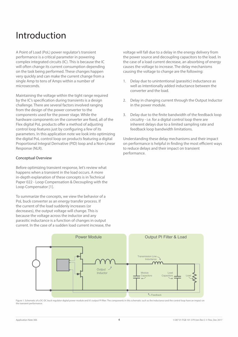
Our example uses a BMR 464 0x02/001 set to output 1.0V. The output filter configured in FPD’s loop compensator is as shown in Figure 2. As shown, the module has a collection of module and load-side capacitors with related Equivalent Series Resistance (ESR) values, combined with transmission line impedance and inductance. This arrangement of capacitance and inductance forms what’s known as a capacitor-input filter, or pi filter. The values chosen for the capacitance can typically be found in the load IC’s datasheet. More information on designing the pi filter can be found in AN321 - Output Filter Impedance Design [3].
Figure 2. Setup of the output filter. On the module-side there is one 470μF bulk capacitor and three 40μF ceramic capacitors, all with ESR values of 10mΩ. On the load-side there is two 220μF bulk capacitors and ten 20μF ceramic capacitors, with ESR values of 10mΩ and 5mΩ respectively.
Loop stability requirements are left at their defaults for this example, and loop transient requirements are as shown in Table 1. These requirements can be typically found in the load IC’s datasheet.
Load Transient Requirement
Value used in Example
Max Deviation 30mV (3% of 1V output)
Recovery Time 100μs
Recovery Limit 10mV (1% of 1V output)
Table 1. Setup of load transient response requirements.
Finally, we set some load transient simulation parameters to view the results of our output filter and PID coefficients. Typically in our engineering tests for characterization we will test a load transient of 25-75% of the product’s maximum current. However sometimes in real-world examples it may not be possible to do this due to limitations in how much current can be delivered through the vias and board itself. In this example (shown in Table 2) we use a 25-50% load step as our intent is to optimize loop behavior. We choose this value so we can practically compare results on an actual board, presented later in the section “Optimizing with Non-Linear Response”.
Transient Response Simulation Parameters
Value used in Example
Load Current Transition 10A to 20A (25-50% of BMR464’s 40A max)
Slew Rate 5A/μs
Step period 2ms
Vout Droop 0mV/A
Table 2. Setup of the load transient response simulation parameters.
NOTE: The BMR464 0x02/001 is used for this example because it has fixed factory-set PID settings. Modules with Dynamic Loop Compensation (such as BMR 464 0x08/001) are shipped with DLC enabled and as a result, actual PID settings are calculated by the DLC algorithm after the unit is turned on. For a unit with DLC enabled, the PID settings shown in the simulator are only used during the initial ramp-up, and are not relevant for simulating normal operation. For more information on DLC, please refer to the BMR464 0x008/001 Technical Specification [4].
Application Note 306 5 1/287 01-FGB 101 379 Uen Rev C © Flex, Dec 2017
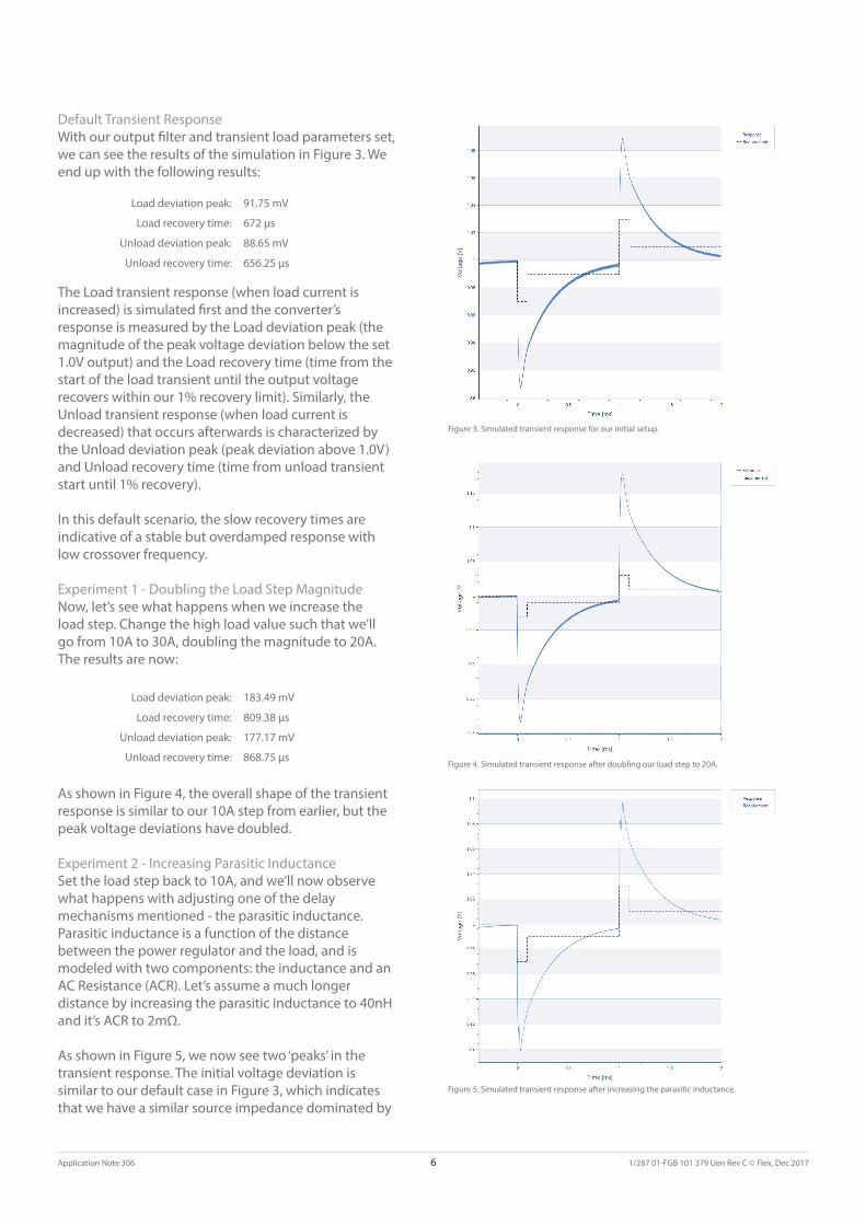
Default Transient Response With our output filter and transient load parameters set, we can see the results of the simulation in Figure 3. We end up with the following results:
Load deviation peak: 91.75 mV
Load recovery time: 672 μs
Unload deviation peak: 88.65 mV
Unload recovery time: 656.25 μs
The Load transient response (when load current is increased) is simulated first and the converter’s response is measured by the Load deviation peak (the magnitude of the peak voltage deviation below the set 1.0V output) and the Load recovery time (time from the start of the load transient until the output voltage recovers within our 1% recovery limit). Similarly, the Unload transient response (when load current is decreased) that occurs afterwards is characterized by the Unload deviation peak (peak deviation above 1.0V) and Unload recovery time (time from unload transient start until 1% recovery).
In this default scenario, the slow recovery times are indicative of a stable but overdamped response with low crossover frequency.
Experiment 1 - Doubling the Load Step MagnitudeNow, let’s see what happens when we increase the load step. Change the high load value such that we’ll go from 10A to 30A, doubling the magnitude to 20A. The results are now:
Load deviation peak: 183.49 mV
Load recovery time: 809.38 μs
Unload deviation peak: 177.17 mV
Unload recovery time: 868.75 μs
As shown in Figure 4, the overall shape of the transient response is similar to our 10A step from earlier, but the peak voltage deviations have doubled.
Experiment 2 - Increasing Parasitic InductanceSet the load step back to 10A, and we’ll now observe what happens with adjusting one of the delay mechanisms mentioned - the parasitic inductance. Parasitic inductance is a function of the distance between the power regulator and the load, and is modeled with two components: the inductance and an AC Resistance (ACR). Let’s assume a much longer distance by increasing the parasitic inductance to 40nH and it’s ACR to 2mΩ.
As shown in Figure 5, we now see two ‘peaks’ in the transient response. The initial voltage deviation is similar to our default case in Figure 3, which indicates that we have a similar source impedance dominated by
Figure 3. Simulated transient response for our initial setup.
Figure 4. Simulated transient response after doubling our load step to 20A.
Figure 5. Simulated transient response after increasing the parasitic inductance.
Application Note 306 6 1/287 01-FGB 101 379 Uen Rev C © Flex, Dec 2017
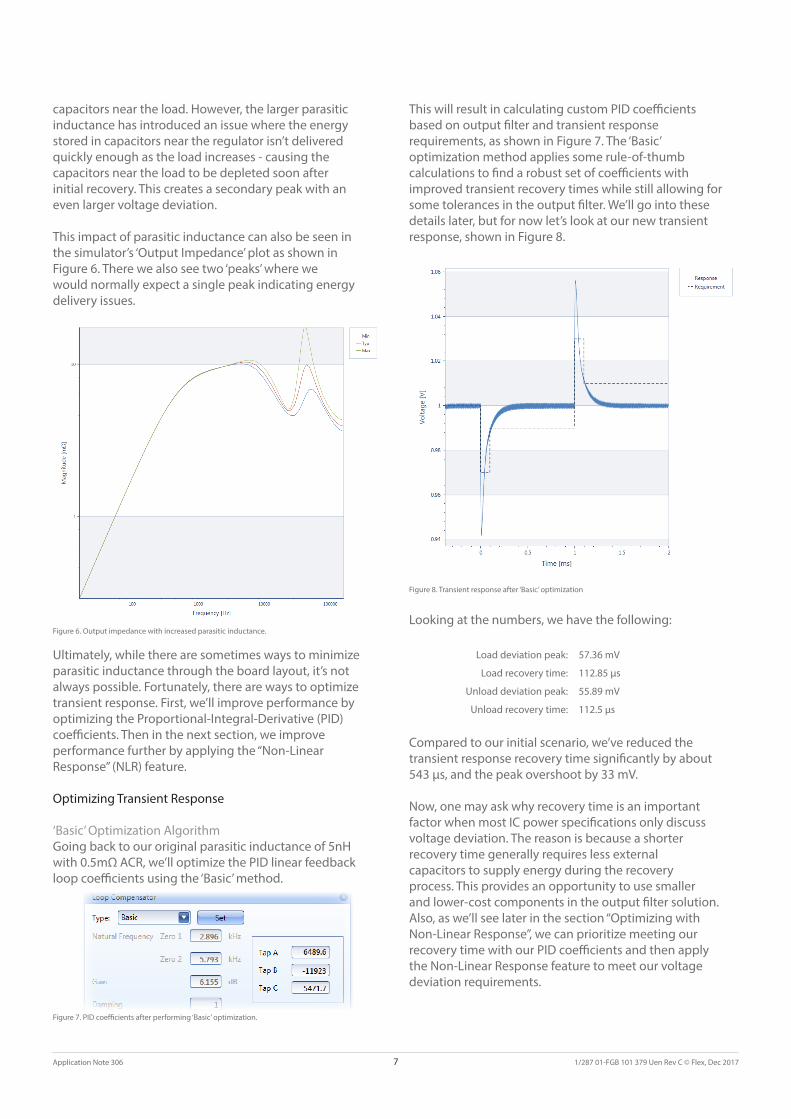
capacitors near the load. However, the larger parasitic inductance has introduced an issue where the energy stored in capacitors near the regulator isn’t delivered quickly enough as the load increases - causing the capacitors near the load to be depleted soon after initial recovery. This creates a secondary peak with an even larger voltage deviation.
This impact of parasitic inductance can also be seen in the simulator’s ‘Output Impedance’ plot as shown in Figure 6. There we also see two ‘peaks’ where we would normally expect a single peak indicating energy delivery issues.
Figure 6. Output impedance with increased parasitic inductance.
Ultimately, while there are sometimes ways to minimize parasitic inductance through the board layout, it’s not always possible. Fortunately, there are ways to optimize transient response. First, we’ll improve performance by optimizing the Proportional-Integral-Derivative (PID) coefficients. Then in the next section, we improve performance further by applying the “Non-Linear Response” (NLR) feature.
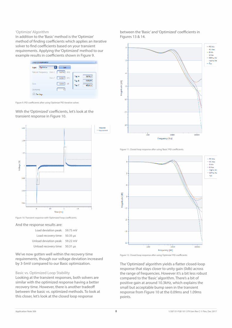
Optimizing Transient Response ‘Basic’ Optimization Algorithm Going back to our original parasitic inductance of 5nH with 0.5mΩ ACR, we’ll optimize the PID linear feedback loop coefficients using the ‘Basic’ method.
Figure 7. PID coefficients after performing ‘Basic’ optimization.
This will result in calculating custom PID coefficients based on output filter and transient response requirements, as shown in Figure 7. The ‘Basic’ optimization method applies some rule-of-thumb calculations to find a robust set of coefficients with improved transient recovery times while still allowing for some tolerances in the output filter. We’ll go into these details later, but for now let’s look at our new transient response, shown in Figure 8.
Figure 8. Transient response after ‘Basic’ optimization
Looking at the numbers, we have the following:
Load deviation peak: 57.36 mV
Load recovery time: 112.85 μs
Unload deviation peak: 55.89 mV
Unload recovery time: 112.5 μs
Compared to our initial scenario, we’ve reduced the transient response recovery time significantly by about 543 μs, and the peak overshoot by 33 mV.
Now, one may ask why recovery time is an important factor when most IC power specifications only discuss voltage deviation. The reason is because a shorter recovery time generally requires less external capacitors to supply energy during the recovery process. This provides an opportunity to use smaller and lower-cost components in the output filter solution. Also, as we’ll see later in the section “Optimizing with Non-Linear Response”, we can prioritize meeting our recovery time with our PID coefficients and then apply the Non-Linear Response feature to meet our voltage deviation requirements.
Application Note 306 7 1/287 01-FGB 101 379 Uen Rev C © Flex, Dec 2017
‘Optimize’ Algorithm In addition to the ‘Basic’ method is the ‘Optimize’ method of finding coefficients which applies an iterative solver to find coefficients based on your transient requirements. Applying the ‘Optimized’ method to our example results in coefficients shown in Figure 9.
Figure 9. PID coefficients after using ‘Optimize’ PID iterative solver.
With the ‘Optimized’ coefficients, let’s look at the transient response in Figure 10.
Figure 10. Transient response with ‘Optimized’ loop coefficients.
And the response results are:Load deviation peak: 59.75 mV
Load recovery time: 50.35 μs
Unload deviation peak: 59.22 mV
Unload recovery time: 50.31 μs
We’ve now gotten well within the recovery time requirements, though our voltage deviation increased by 3-5mV compared to our Basic optimization.
Basic vs. Optimized Loop Stability Looking at the transient responses, both solvers are similar with the optimized response having a better recovery time. However, there is another tradeoff between the basic vs. optimized methods. To look at this closer, let’s look at the closed loop response
between the ‘Basic’ and ‘Optimized’ coefficients in Figures 13 & 14.
Figure 11. Closed loop response after using ‘Basic’ PID coefficients.
Figure 12. Closed loop response after using ‘Optimize’ PID coefficients
The ‘Optimized’ algorithm yields a flatter closed-loop response that stays closer to unity gain (0db) across the range of frequencies. However it’s a bit less robust compared to the ‘Basic’ algorithm. There’s a bit of positive gain at around 10.3kHz, which explains the small but acceptable bump seen in the transient response from Figure 10 at the 0.09ms and 1.09ms points.
Application Note 306 8 1/287 01-FGB 101 379 Uen Rev C © Flex, Dec 2017
Generally, the ‘Optimized’ algorithm results in more aggressive loop performance that reacts faster to changes, at the tradeoff of making the loop more sensitive to the component values in the output filter. This means applying the Optimized algorithm without properly representing the capacitors or the parasitic inductance may result in ringing or even oscillation in the response. This tradeoff is not a hard rule though - there are scenarios where the optimized algorithm may yield a more robust set of coefficients than the basic algorithm. Ultimately one should test and compare both the Basic and Optimized algorithms for their actual requirements and output filter design.
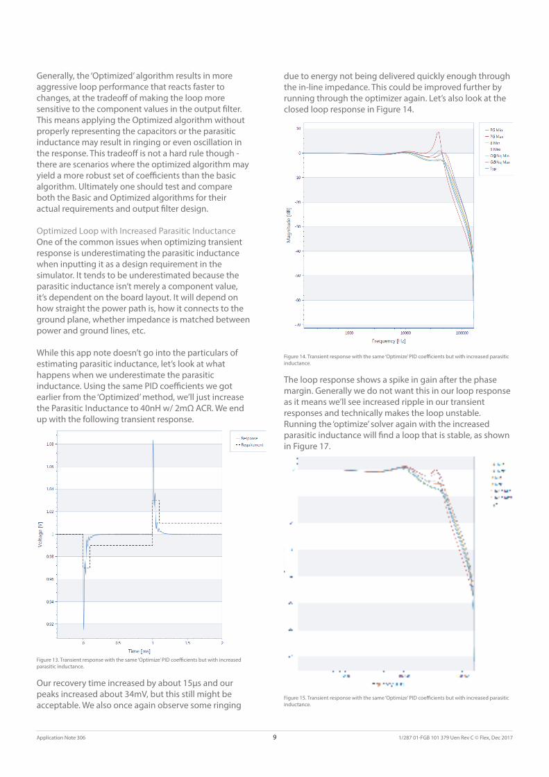
Optimized Loop with Increased Parasitic Inductance One of the common issues when optimizing transient response is underestimating the parasitic inductance when inputting it as a design requirement in the simulator. It tends to be underestimated because the parasitic inductance isn’t merely a component value, it’s dependent on the board layout. It will depend on how straight the power path is, how it connects to the ground plane, whether impedance is matched between power and ground lines, etc.
While this app note doesn’t go into the particulars of estimating parasitic inductance, let’s look at what happens when we underestimate the parasitic inductance. Using the same PID coefficients we got earlier from the ‘Optimized’ method, we’ll just increase the Parasitic Inductance to 40nH w/ 2mΩ ACR. We end up with the following transient response.
Figure 13. Transient response with the same ‘Optimize’ PID coefficients but with increased parasitic inductance.
Our recovery time increased by about 15μs and our peaks increased about 34mV, but this still might be acceptable. We also once again observe some ringing
due to energy not being delivered quickly enough through the in-line impedance. This could be improved further by running through the optimizer again. Let’s also look at the closed loop response in Figure 14.
Figure 14. Transient response with the same ‘Optimize’ PID coefficients but with increased parasitic inductance.
The loop response shows a spike in gain after the phase margin. Generally we do not want this in our loop response as it means we’ll see increased ripple in our transient responses and technically makes the loop unstable. Running the ‘optimize’ solver again with the increased parasitic inductance will find a loop that is stable, as shown in Figure 17.
Figure 15. Transient response with the same ‘Optimize’ PID coefficients but with increased parasitic inductance.
Application Note 306 9 1/287 01-FGB 101 379 Uen Rev C © Flex, Dec 2017
Optimizing with Non-Linear Response
So far we’ve seen how optimizing the feedback loop’s PID coefficients yields an improved transient response. This process of improvement is similar to that of a traditional analog feedback loop, but with the advantage of a much faster time of implementing changes. This is because we’re working with a digital PID loop that doesn’t require hardware changes to adjust loop coefficients.
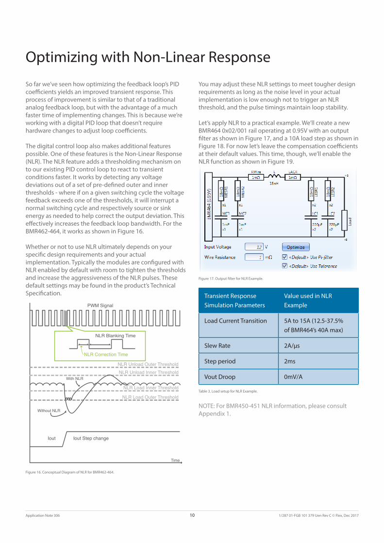
The digital control loop also makes additional features possible. One of these features is the Non-Linear Response (NLR). The NLR feature adds a thresholding mechanism on to our existing PID control loop to react to transient conditions faster. It works by detecting any voltage deviations out of a set of pre-defined outer and inner thresholds - where if on a given switching cycle the voltage feedback exceeds one of the thresholds, it will interrupt a normal switching cycle and respectively source or sink energy as needed to help correct the output deviation. This effectively increases the feedback loop bandwidth. For the BMR462-464, it works as shown in Figure 16.
Whether or not to use NLR ultimately depends on your specific design requirements and your actual implementation. Typically the modules are configured with NLR enabled by default with room to tighten the thresholds and increase the aggressiveness of the NLR pulses. These default settings may be found in the product’s Technical Specification.
NLR Correction Time
NLR Blanking Time
NLR Unload Outer ThresholdNLR Unload Inner Threshold
NLR Load Inner Threshold
NLR Load Outer Threshold
PWM Signal
Iout Step changeIout
Without NLR
With NLR
Time
Figure 16. Conceptual Diagram of NLR for BMR462-464.
You may adjust these NLR settings to meet tougher design requirements as long as the noise level in your actual implementation is low enough not to trigger an NLR threshold, and the pulse timings maintain loop stability. Let’s apply NLR to a practical example. We’ll create a new BMR464 0x02/001 rail operating at 0.95V with an output filter as shown in Figure 17, and a 10A load step as shown in Figure 18. For now let’s leave the compensation coefficients at their default values. This time, though, we’ll enable the NLR function as shown in Figure 19.
Figure 17. Output filter for NLR Example.
Transient Response Simulation Parameters
Value used in NLR Example
Load Current Transition 5A to 15A (12.5-37.5% of BMR464’s 40A max)
Slew Rate 2A/μs
Step period 2ms
Vout Droop 0mV/A
Table 3. Load setup for NLR Example.
NOTE: For BMR450-451 NLR information, please consult Appendix 1.
Application Note 306 10 1/287 01-FGB 101 379 Uen Rev C © Flex, Dec 2017
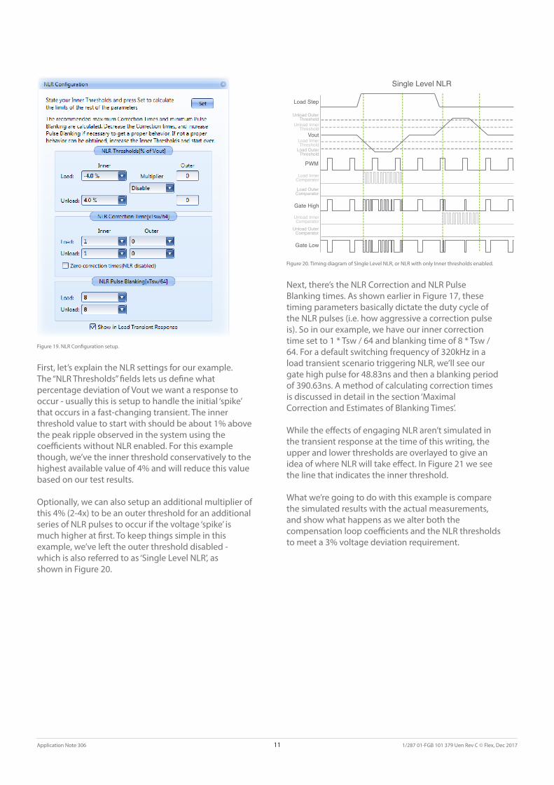
Figure 19. NLR Configuration setup.
First, let’s explain the NLR settings for our example. The “NLR Thresholds” fields lets us define what percentage deviation of Vout we want a response to occur - usually this is setup to handle the initial ‘spike’ that occurs in a fast-changing transient. The inner threshold value to start with should be about 1% above the peak ripple observed in the system using the coefficients without NLR enabled. For this example though, we’ve the inner threshold conservatively to the highest available value of 4% and will reduce this value based on our test results.
Optionally, we can also setup an additional multiplier of this 4% (2-4x) to be an outer threshold for an additional series of NLR pulses to occur if the voltage ‘spike’ is much higher at first. To keep things simple in this example, we’ve left the outer threshold disabled - which is also referred to as ‘Single Level NLR’, as shown in Figure 20.
Load Step
Unload InnerThreshold
Unload OuterThreshold
VoutLoad InnerThreshold
Load OuterThreshold
PWM
Load InnerComparator
Load OuterComparator
Gate High
Gate Low
Unload OuterComparator
Unload InnerComparator
Single Level NLR
Figure 20. Timing diagram of Single Level NLR, or NLR with only Inner thresholds enabled.
Next, there’s the NLR Correction and NLR Pulse Blanking times. As shown earlier in Figure 17, these timing parameters basically dictate the duty cycle of the NLR pulses (i.e. how aggressive a correction pulse is). So in our example, we have our inner correction time set to 1 * Tsw / 64 and blanking time of 8 * Tsw / 64. For a default switching frequency of 320kHz in a load transient scenario triggering NLR, we’ll see our gate high pulse for 48.83ns and then a blanking period of 390.63ns. A method of calculating correction times is discussed in detail in the section ‘Maximal Correction and Estimates of Blanking Times’.
While the effects of engaging NLR aren’t simulated in the transient response at the time of this writing, the upper and lower thresholds are overlayed to give an idea of where NLR will take effect. In Figure 21 we see the line that indicates the inner threshold.
What we’re going to do with this example is compare the simulated results with the actual measurements, and show what happens as we alter both the compensation loop coefficients and the NLR thresholds to meet a 3% voltage deviation requirement.
Application Note 306 11 1/287 01-FGB 101 379 Uen Rev C © Flex, Dec 2017
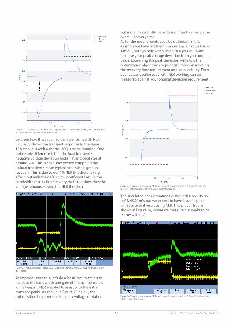
Figure 21. Transient response of NLR example with default PID coefficients, and markers (not simulation) of -/+ 4% NLR inner thresholds.
Let’s see how this circuit actually performs with NLR. Figure 22 shows the transient response to the same 10A step, but with a shorter 300μs pulse duration. One noticeable difference is that the load transient’s negative voltage deviation looks flat and oscillates at around -4%. This is a bit unexpected compared the unload transient’s more typical peak with a gradual recovery. This is due to our 4% NLR threshold taking effect, but with the default PID coefficients setup, the bandwidth results in a recovery that’s too slow, thus the voltage remains around the NLR threshold.
Figure 22. Actual results of NLR example with default PID coefficients and -/+ 4% NLR inner thresholds.
To improve upon this, let’s do a ‘basic’ optimization to increase the bandwidth and gain of the compensator, while keeping NLR enabled to assist with the initial transient peaks. As shown in Figure 23 below, the optimization helps reduce the peak voltage deviation
but more importantly helps to significantly shorten the overall recovery time. As for the requirements used by optimizer, in this example we have left them the same as what we had in Table 1, but typically when using NLR you will want increase your peak voltage deviation from your original value. Loosening the peak deviation will allow the optimization algorithms to prioritize more on meeting the recovery time requirement and loop stability. Then your actual oscilloscope with NLR working can be measured against your original deviation requirement.
Figure 23. Transient response of NLR example with ‘basic’ optimized PID coefficients, and markers (not simulation) of -/+ 4% NLR inner thresholds.
The simulated peak deviations without NLR are -45.96 mV & 45.21mV, but we expect to have less of a peak with our actual result using NLR. This proves true as shown in Figure 24, where we measure our peaks to be -43mV & 41mV.
Figure 24. Transient response of NLR example with ‘basic’ optimized PID coefficients and -/+ 4% NLR inner thresholds.
Application Note 306 12 1/287 01-FGB 101 379 Uen Rev C © Flex, Dec 2017
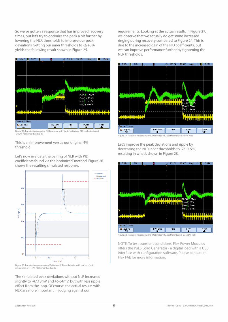
So we’ve gotten a response that has improved recovery times, but let’s try to optimize the peak a bit further by lowering the NLR thresholds to improve our peak deviations. Setting our inner thresholds to -2/+3% yields the following result shown in Figure 25.
Figure 25. Transient response of NLR example with ‘basic’ optimized PID coefficients and -2/+3% NLR inner thresholds.
This is an improvement versus our original 4% threshold.
Let’s now evaluate the pairing of NLR with PID coefficients found via the ‘optimized’ method. Figure 26 shows the resulting simulated response.
Figure 26. Transient response using ‘Optimized’ PID coefficients, with markers (not simulation) of -/+ 4% NLR inner thresholds.
The simulated peak deviations without NLR increased slightly to -47.18mV and 46.64mV, but with less ripple effect from the loop. Of course, the actual results with NLR are more important in judging against our
requirements. Looking at the actual results in Figure 27, we observe that we actually do get some increased ringing during recovery compared to Figure 24. This is due to the increased gain of the PID coefficients, but we can improve performance further by tightening the NLR thresholds.
Figure 27. Transient response using ‘Optimized’ PID coefficients and -/+4% NLR
Let’s improve the peak deviations and ripple by decreasing the NLR inner thresholds to -2/+2.5%, resulting in what’s shown in Figure 28.
Figure 28. Transient response using ‘Optimized’ PID coefficients and -2/+2.5% NLR
NOTE: To test transient conditions, Flex Power Modules offers the PuLS Load Generator - a digital load with a USB interface with configuration software. Please contact an Flex FAE for more information.
Application Note 306 13 1/287 01-FGB 101 379 Uen Rev C © Flex, Dec 2017

Transient Optimization Workflow To summarize, we took the following steps to optimize the transient response:
1. In the Flex Power Designer loop compensator tool, create a model of an output filter that includes an accurate approximation of parasitic impedance and output capacitance (both near the module and near the load). - Be sure to enter capacitance Equivalent Series Resistance (ESR) values that are consistent with frequency range near the module’s crossover frequency (i.e. bandwidth) - more on this is written in the ‘Output Filter ESR Calculation’ below in the section ‘Additional Design Considerations’.
2. Set transient response requirements. Initially, you may start by setting the response requirements to those found from the Load IC Datasheet. If desired performance can’t be met with the default NLR settings, you may modify the peak deviation requirement to be less strict by increasing the peak deviation value. This requirement is loosened to allow the PID optimization to prioritize meeting the recovery time requirement. The actual peak deviation requirement can then be met via adjusting NLR settings.
3. Evaluate both the ‘basic’ and ‘optimized’ solvers to find PID coefficients. Start by ensuring that one of the loop optimization methods yields a transient response simulation that meets your transient requirements and is stable. If neither method can meet your requirements, consider using NLR and adjust requirements as suggested in step two, iteratively adjusting the peak deviation requirement until you can meet your recovery time. Later, you’ll adjust the NLR settings to reduce the peak deviation to meet the original requirements.
4. Configure your module(s) using the PID coefficients found in step three. Then attach the module to a transient load similar to your simulation (such as the Flex PuLS Load Generator) and measure the actual transient response on an oscilloscope. This helps you confirm your loop is stable, provides a reference point for later comparison, and the measured voltage ripple and noise of the transient response will be used to determine the initial NLR threshold.
5. If you decided to adjust the NLR settings beyond their
defaults, go back to the Flex Power Designer loop compensator tool and setup NLR parameters per the following guidelines: - NLR Thresholds: should be set between 0.5% to 1.0% above the output voltage peak ripple and noise to avoid unintentional NLR pulses. The peak ripple should be found in step 3 by measuring the transient response with NLR temporarily disabled. For example, if you measure the noise to be 0.9% above the output voltage, the NLR threshold should initially be set to at 2%. Thresholds should be found this way unless mentioned otherwise in the product’s datasheet. - Correction & Recovery times: Set Correction & Recovery times using the equations detailed later in the section ‘Maximal Correction and Estimates of Blanking Times’ or by using the ‘Set’ button to automatically calculate initial values based on the Inner Thresholds then adjust as necessary. These timings will determine the aggressiveness of the NLR pulses. - NLR Mode: Beyond just the “Single Level NLR” mode measured in the previous example, there are “Dual Level NLR” and “Hysteretic NLR” modes that allow for a more aggressive response for higher voltage deviations. Refer to the section “Non-Linear Response Advanced Usage” for details on which mode to use. - NLR works best when the output impedance is minimized. Furthermore, as observed in comparing Figure 25 to Figure 28, the performance of the PID coefficients will influence the performance of the NLR circuit.
6. Configure your module(s) with your PID coefficients and NLR settings, and measure the actual transient performance again to see if you are meeting requirements with a stable transient response. - When a transient response is causing more than two overshoots, it may be due to the additional NLR pulses increasing the effective switching frequency. This may lead to a reduction in the overall power supply efficiency. To fix this, the correction and blanking time may need to be optimized until a balance between improved transient response and minimized overshoots is met.
Application Note 306 14 1/287 01-FGB 101 379 Uen Rev C © Flex, Dec 2017

Additional Design Considerations
Beyond this workflow, there are additional design considerations to ensure a stable and expected response:
Output Filter ESR CalculationSetting the capacitor’s ESR accurately is an iterative process - where you start conservatively with a higher than nominal ESR value, observe the resultant bandwidth calculated from the loop simulation, then decrease it as needed. You can find the ESR data from the component manufacturer such as Murata’s ‘SimSerfing’ online tool.
Capacitor Selection for NLR / Damping For the best flexibility in adjusting NLR settings, it is important for the power filter to accommodate optimal damping. This means that the output filter can respond to a transient with the most direct and minimal response. Filters with very little damping may limit the choices of NLR settings and overall performance gains of NLR. Suitable damping can be added through the choice of capacitors near the regulator’s output. Usually, capacitors with a low ESR, such as monolithic ceramic capacitors, are used to filter the ripple current. Additional bulk electrolytic capacitors are added to support the charge storage for transient loads.
Voltage Remote Sensing & NLR Because the NLR circuit samples the output voltage at a high speed (64 * Fsw), there is a risk of it responding to perturbations shorter than one switching cycle. Care should be taken in routing the remote sensing terminals - they should be routed as a differential pair, and preferably between signal ground planes that are not carrying high currents. The routing should avoid areas of high electric fields (such as the switching or gate drive nodes in the power stage) or magnetic fields (such as in the vicinity of a power inductor).
Current Sense & NLR The design of the BMR462-464/BMR466 regulators guarantee sampling of the output current for overcurrent protection even when NLR pulses are occurring. In order to accomplish current sampling, NLR activity will be suspended until a valid current sample is measured. This happens no later than the third switching cycle after NLR pulses begin. NLR resumes once the current measurement occurs. This may result in a perturbation of the voltage recovery, but is designed this way to provide protection from a catastrophic fault.
Voltage Droop The VOUT_DROOP command lets one specify the expected output load-line resistance in mV/A. When this is set to a positive non-zero value, it will decrease the output voltage setpoint in proportion to the measured load current. This function can be used to improve the transient envelope of the converter by as much of a factor of two. The NLR thresholds also adjust to stay relative to the target voltage of the droop function.
Since the droop function is dependent on measured current though, there is some delay (Tsw / 16) due to the digital filtering for the current. This means there will be some delay observed when tested against a step load function.
The droop resistance value can be determined by the maximum rated load current, and the transient voltage deviation requirements. The following equation calculates the droop value:
VO_Droop = ΔVO_PP / IO_Rated
Where:• ΔVO_PP is the difference between the maximum
positive and negative voltage deviation requirements in mV. This is the total transient voltage deviation budget.
• IO_Rated is the rated maximum load current in Amperes.
• VO_Droop is the droop parameter calculated in mV/A.
This calculation may be extended to include parasitic resistances (particularly for current sharing groups) or other constraints on the droop.
Current Sharing & NLR When the BMR462-464/BMR466 regulators are used in parallel for current sharing, the NLR thresholds are automatically scaled (known as threshold scaling), and a minimum droop value is set. For more details, see application note AN307 on current sharing.
Application Note 306 15 1/287 01-FGB 101 379 Uen Rev C © Flex, Dec 2017
Maximal Correction and Estimates of Blanking Times
In our earlier example, we chose a relatively conservative correction time of 1 * Tsw / 64 with a blanking time of 8 * Tsw / 64. What we could have also done is calculated the maximum correction time to safely experiment with a more aggressive transient correction time.
Calculating Correction TimeThe maximum correction time may be estimated for the output filter as long as the damping is not too excessive. To do this, we first assume that the ‘correction current’ needed to cause (or correct) a voltage deviation is:
ΔIL = ΔVO / ZO
Where:• ΔIL is the required correction current.• ΔVO is the error in the output voltage, assumed to
be equal to the threshold value. Note that this is for either just the load deviation or the unload deviation, not the maximum of both combined.
• ZO is the output filter’s characteristic impedance, calculated as √( L / C )
Once the correction current is found, the NLR correction units NLoad & NUnload can be estimated from these equations:
NLoad
NUnload =
= (V - V )In Out
( L * ΔI * 64 * F )L(Load) SWNLoad
( L * ΔV * 64 * F ) O(Load) SW
√ LC*
NUnload =( L * ΔV * 64 * F ) O(Unload) SW
√ LC*
( L * ΔI * 64 * F )L(Unload) SW
VOut
(V - V )In Out
VOut
NLoad-Blanking = NLoad(V - V )In Out
VOut*
NUnload-Blanking = NUnload (V - V )In Out
VOut*
=
Where:• NLoad & NUnload are the calculated correction time
units, rounded down to the next lower integer.• L is the inductor value.• VIn is the input voltage.• VOut is the output voltage.
Merging in our correction current equation, we can also express the equations as:
NLoad
NUnload =
= (V - V )In Out
( L * ΔI * 64 * F )L(Load) SWNLoad
( L * ΔV * 64 * F ) O(Load) SW
√ LC*
NUnload =( L * ΔV * 64 * F ) O(Unload) SW
√ LC*
( L * ΔI * 64 * F )L(Unload) SW
VOut
(V - V )In Out
VOut
NLoad-Blanking = NLoad(V - V )In Out
VOut*
NUnload-Blanking = NUnload (V - V )In Out
VOut*
=
Calculating Blanking TimeUsing the calculations of the correction times, we can also calculate some initial baseline blanking times using the following equations:
NLoad
NUnload =
= (V - V )In Out
( L * ΔI * 64 * F )L(Load) SWNLoad
( L * ΔV * 64 * F ) O(Load) SW
√ LC*
NUnload =( L * ΔV * 64 * F ) O(Unload) SW
√ LC*
( L * ΔI * 64 * F )L(Unload) SW
VOut
(V - V )In Out
VOut
NLoad-Blanking = NLoad(V - V )In Out
VOut*
NUnload-Blanking = NUnload (V - V )In Out
VOut*
=NLoad
NUnload =
= (V - V )In Out
( L * ΔI * 64 * F )L(Load) SWNLoad
( L * ΔV * 64 * F ) O(Load) SW
√ LC*
NUnload =( L * ΔV * 64 * F ) O(Unload) SW
√ LC*
( L * ΔI * 64 * F )L(Unload) SW
VOut
(V - V )In Out
VOut
NLoad-Blanking = NLoad(V - V )In Out
VOut*
NUnload-Blanking = NUnload (V - V )In Out
VOut*
=
The blanking times calculated here represent a safe baseline to start with. From here one can experiment with decreasing the blanking times for a more aggressive NLR response.
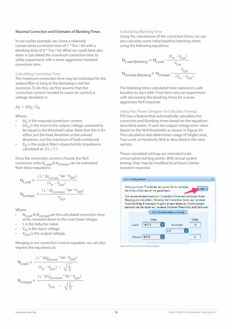
Using Flex Power Designer To Calculate TimingsFPD has a feature that automatically calculates the correction and blanking times based on the equations described earlier. It uses the output voltage error value based on the NLR thresholds as shown in Figure 29. This calculation also determines usage of Single Level, Two Level, or Hysteretic NLR as described in the next section.
These calculated settings are intended to be conservative starting points. With actual system testing, they may be modified to achieve a better transient response.
Figure 29. Two Level NLR Timing Diagram
Application Note 306 16 1/287 01-FGB 101 379 Uen Rev C © Flex, Dec 2017
Non-Linear Response Advanced Usage
While our example earlier was able to meet our requirements with just a ‘single level’ NLR configuration, there may be scenarios where more aggressive control of the transient response is needed. In these cases we make use of the NLR’s outer comparator which enables use of two modes: Two Level NLR and Hysteretic NLR. This section covers these additional modes and discusses which mode to apply for your system.
Two Level NLR
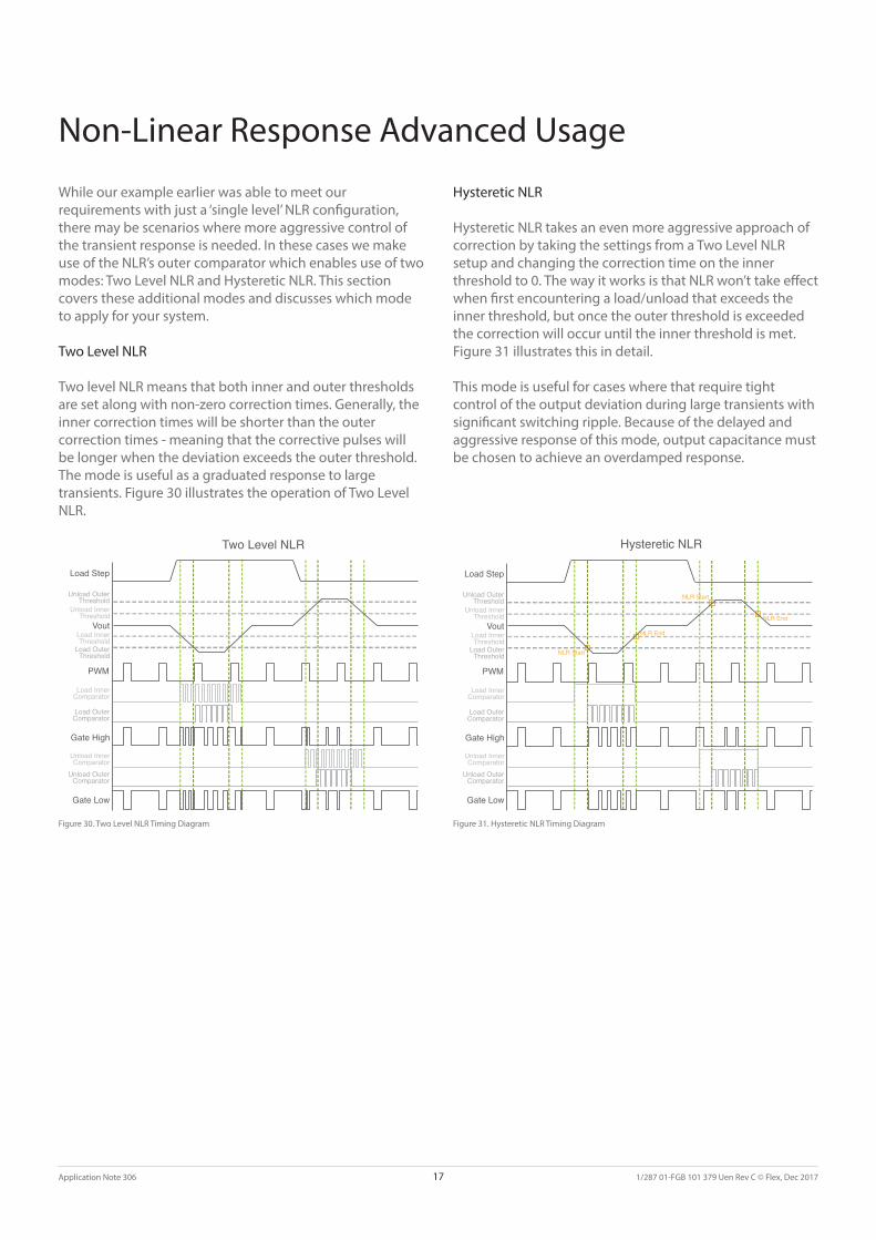
Two level NLR means that both inner and outer thresholds are set along with non-zero correction times. Generally, the inner correction times will be shorter than the outer correction times - meaning that the corrective pulses will be longer when the deviation exceeds the outer threshold. The mode is useful as a graduated response to large transients. Figure 30 illustrates the operation of Two Level NLR.
Load Step
Unload InnerThreshold
Unload OuterThreshold
VoutLoad InnerThreshold
Load OuterThreshold
PWM
Load InnerComparator
Load OuterComparator
Gate High
Gate Low
Unload OuterComparator
Unload InnerComparator
Two Level NLR
Figure 30. Two Level NLR Timing Diagram
Hysteretic NLR
Hysteretic NLR takes an even more aggressive approach of correction by taking the settings from a Two Level NLR setup and changing the correction time on the inner threshold to 0. The way it works is that NLR won’t take effect when first encountering a load/unload that exceeds the inner threshold, but once the outer threshold is exceeded the correction will occur until the inner threshold is met. Figure 31 illustrates this in detail.
This mode is useful for cases where that require tight control of the output deviation during large transients with significant switching ripple. Because of the delayed and aggressive response of this mode, output capacitance must be chosen to achieve an overdamped response.
Load Step
Unload InnerThreshold
Unload OuterThreshold
VoutLoad InnerThreshold
Load OuterThreshold
PWM
Load InnerComparator
Load OuterComparator
Gate High
Gate Low
Unload OuterComparator
Unload InnerComparator
Hysteretic NLR
NLR Start
NLR End
NLR End
NLR Start
Figure 31. Hysteretic NLR Timing Diagram
Application Note 306 17 1/287 01-FGB 101 379 Uen Rev C © Flex, Dec 2017
NLR Mode Selection Guide
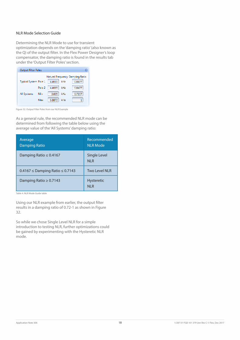
Determining the NLR Mode to use for transient optimization depends on the ‘damping ratio’ (also known as the Q) of the output filter. In the Flex Power Designer’s loop compensator, the damping ratio is found in the results tab under the ‘Output Filter Poles’ section.
Figure 32. Output Filter Poles from our NLR Example
As a general rule, the recommended NLR mode can be determined from following the table below using the average value of the ‘All Systems’ damping ratio:
Average Damping Ratio
Recommended NLR Mode
Damping Ratio ≤ 0.4167 Single Level NLR
0.4167 ≤ Damping Ratio ≤ 0.7143 Two Level NLR
Damping Ratio ≥ 0.7143 Hysteretic NLR
Table 4. NLR Mode Guide table
Using our NLR example from earlier, the output filter results in a damping ratio of 0.72-1 as shown in Figure 32.
So while we chose Single Level NLR for a simple introduction to testing NLR, further optimizations could be gained by experimenting with the Hysteretic NLR mode.
Application Note 306 18 1/287 01-FGB 101 379 Uen Rev C © Flex, Dec 2017
Appendix 1: NLR feature on BMR450/451
Other BMR450-451 uses an earlier generation of NLR that has some differences compared to the NLR used in our examples using the BMR462-464.
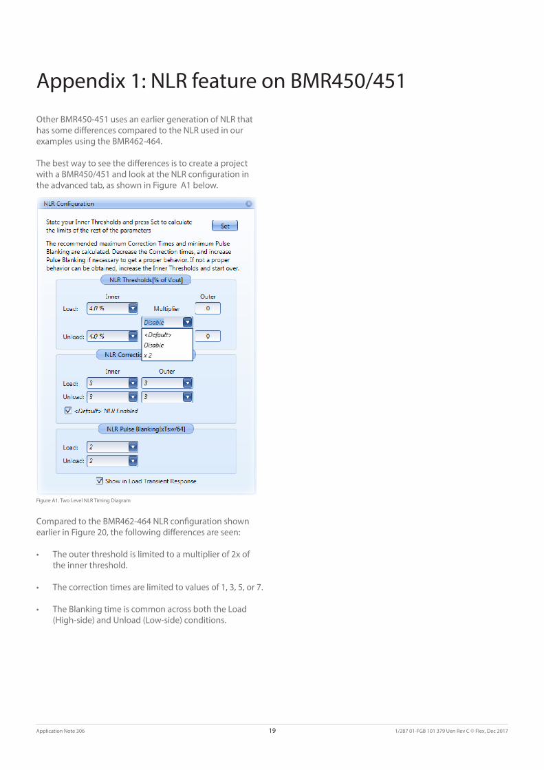
The best way to see the differences is to create a project with a BMR450/451 and look at the NLR configuration in the advanced tab, as shown in Figure A1 below.
Figure A1. Two Level NLR Timing Diagram
Compared to the BMR462-464 NLR configuration shown earlier in Figure 20, the following differences are seen:
• The outer threshold is limited to a multiplier of 2x of the inner threshold.
• The correction times are limited to values of 1, 3, 5, or 7.
• The Blanking time is common across both the Load (High-side) and Unload (Low-side) conditions.
Application Note 306 19 1/287 01-FGB 101 379 Uen Rev C © Flex, Dec 2017

References
[1] - Technical Paper 022 - Loop Compensation & Decoupling with the Loop Compensator.
[2] - Flex Power Designer User Guide - bundled with the Flex Power Designer and available at www.digitalpowerdesigner.com.
[3] - AN321 - Output Filter Impedance Design.
[4] - BMR464 0x008/001 Technical Specification.
Application Note 306 20 1/287 01-FGB 101 379 Uen Rev C © Flex, Dec 2017
Flex Power Modulesflex.com/expertise/power/modules
APPLICATION NOTE1/287 01-FGB 101 379 Uen Rev C
© Flex Dec 2017
Formed in the late seventies, Flex Power Modules is a division of Flex that primarily designs and manufactures isolated DC/DC converters and non-isolated voltage products such as point-of-load units ranging in output power from 1 W to 700 W. The products are aimed at (but not limited to) the new generation of ICT (information and communication technology) equipment where systems’ architects are designing boards for optimized control and reduced power consumption.
Flex Power Modules Torshamnsgatan 28 A164 94 Kista, SwedenEmail: [email protected]
Flex Power Modules - Americas600 Shiloh RoadPlano, Texas 75074, USATelephone: +1-469-229-1000
Flex Power Modules - Asia/PacificFlex Electronics Shanghai Co., Ltd 33 Fuhua Road, Jiading DistrictShanghai 201818, ChinaTelephone: +86 21 5990 3258-26093
The content of this document is subject to revision without notice due to continued progress in methodology, design and manufacturing. Flex shall have no liability for any error or damage of any kind resulting from the use of this document