Embed Size (px)
Citation preview

Optimizing your test and measurement solution by leveraging the industry’s most integrated SoC
Magnus von BrömssenCustomer System Solution Lead
Béatrice PhilibertCTO Radio Access Network
Texas Instruments
Optimizing your test and measurement solution by 2 November 2015 leveraging the industry’s most integrated SoC
1. Introduction
New challenges are brought to the test and measurement (T&M) market with the ever-increasing availability of new technology and with new ways to connect and interact between man and machine as well as machine to machine. New future-proof and cost efficient T&M products are required to enable effective test and validation not only during product development and product manufacturing, but also throughout the lifetime of the product.
The T&M market can be divided into three sub-segments, each having specific characteristics. The first segment consists of the general-purpose T&M segment, which includes end applications such as oscilloscopes and signal or logic analyzers/generators. This type of equipment is used in many diverse industry branches from lab to manufacturing test to field test. Another segment is the mechanical test segment, which includes non-destructive testing (NDT), industrial X-ray, material testing and highly accurate measurements of physical dimensions like LIDAR. Finally, the third segment consists of telecommunication testing with products for the wireline, wireless, optical and telecommunication markets.
Requirements of these sub-segments can be met by leveraging the processing capacity and acceleration capability of TI’s two new system-on-chips (SoCs) 66AK2L06 and TCI6630K2L for a cost-effective implementation of T&M products. Both SoCs offer a rich hardware environment as well as a complete software development environment that integrates the functions necessary to generate, process and analyze the signals at all stages, from discrete analog-to-digital converters (ADCs) and digital-to-analog converters (DACs) to the graphical user interface (GUI) connection and external mass storage. The SoCs provide a highly integrated solution with an integrated digital front end (DFE) and a JESD204B interface, enabling seamless connection to high-speed data converters like ADCs, DACs and analog front ends (AFEs). This paper will detail the capabilities and advantages of the 66AK2L06 SoC in the area of general-purpose testers. The paper describes the benefits of the 66AK2L06 SoC for two classes of application: arbitrary signal generators and real-time spectrum analyzers (SAs). The TCI6630K2L SoC is also a cost-effective solution for telecommunication testing products.
2. Application overview
Signal generators are key tools for the T&M
market. They produce well-defined signals that
enable engineers to explore and test their devices.
Early equipment generated simple continuous
waveforms, but as the industry of signal processing
has evolved at a fast pace, test signals have
become more complex and the control demands
on signal generators have increased accordingly.
Not only should a modern signal generator have
the capability to generate the expected modulated
waveform, it should also emulate the impairments
and interference that would impact the signal

Optimizing your test and measurement solution by 3 November 2015 leveraging the industry’s most integrated SoC
under test in the field. Such signal generators are
now widely used across the industry. The most
demanding industries in that respect are wireless
communication, aeronautic, satellite and defense
applications. They require vector signal generators
(VSGs), which produce digitally modulated signals
according to predefined formats. Depending on
the type of measurements, generated signals may
carry information for the purpose of testing user
equipment.
The most common vector measurements are power
measurements like adjacent channel power ratio
(ACPR), sensitivity and selectivity and amplitude/
phase errors like error vector magnitude. Accuracy
of the measurement depends on the accuracy of
the VSG. For example:
1. Power level accuracy affects the measurement
of an equipment sensitivity
2. Amplitude-/phase-level accuracy affects the
measurement of an equipment signal distortion
3. Frequency level accuracy affects the
measurement of an equipment selectivity
Some test applications require that the VSG creates
a very clean signal. This can be difficult as the
signal generator may introduce errors in the signal.
Nevertheless, it is possible to compensate for these
impairments using pre-distortion techniques proven
in the field of radio communications.
The natural companions of signal generators for
the T&M market are SAs. SAs of today range from
cheaper swept-tuned SAs that provide a snap shot
of the signal in the frequency domain, to vector SAs
that add phase information to enable analysis of
digital modulation, to real-time SAs that also provide
the time domain into the spectrum analysis.
Examples of advanced measurement challenges
that modern SAs need to address include:
• Transient and dynamic signal capture and
analysis
• Spread spectrum and frequency hopping
signals
• Burst transmissions, glitches and switching
transients
• Frequency drifting
• Noise analysis
• Modulation analysis including modulation quality
diagnostics
When the equipment to be tested is already
deployed in the field it is necessary to use
portable test equipment. The recent increase in
transceiver equipment has facilitated an increase
in maintenance and test needs in order to ensure
optimal performance of a radio network. It is not
possible to use high-precision laboratory equipment
such as that used for compliance testing or
production testing for on-site testing. Flexible,
portable and less expensive test equipment is
needed for in-field testing. Furthermore, T&M
functionality may be embedded into the equipment
for self-calibration or auto-diagnosis purposes.
Portable, embedded test equipment must balance
flexibility and precision
requirements with reduced
C-SWaP (cost, size, weight and
power), which is also referred
to as SWaP-C (size, weight,
power and cost) in some
regions. Such equipment can
be built around a monolithic
multicore device able to
digitally generate or analyze
complex signals, to apply or
compensate for impairments
while drawing its power supply
from a USB or PoE+ outlet. The 66AK2L06 SoC
and its rich set of libraries address this challenge.
TI’s KeyStone™ SoC-based multicore devices
are at the heart of C-SWaP efficiency, with their
Of particular note is the 66AK2L06 SoC, which delivers a flexible and high- performance devel-opment platform to address advanced measurement and precision require-ments with reduced C-SWaP.

Optimizing your test and measurement solution by 4 November 2015 leveraging the industry’s most integrated SoC
cost-effective performance and low power
consumption. The new TI 66AK2L06 SoC delivers
breakthrough performance and SWaP-C efficiency
to the designers of T&M equipment. Based on
TI’s new KeyStone II multicore architecture, the
66AK2L06 SoC integrates a mix of processing
elements including TI fixed- and floating-point
TMS320C66x digital signal processors (DSPs),
ARM® Cortex®-A15 cores and advanced signal
processing accelerators. The 66AK2L06 SoC is
equipped with a high-speed JESD204B interface for
direct connectivity to TI’s high-speed ADCs, DACs
and AFEs. Integration of a software-programmable
DFE for digital conversion and digital filtering
eliminates the need for what would otherwise be a
set of discrete components, further reducing power
and board space and yielding the best power-per-
watt in a small footprint.
3. Description of device
The use of multiple DSP cores is a key technology
which facilitates increasingly sophisticated signal-
processing algorithms to advance the vanguard of
waveform-intensive applications, such as avionics,
radar, sonar, T&M and radio communications.
Multicore capabilities combined with an expanding
array of AccelerationPacs and an integrated
transport solution enable high performance at
exceptionally low power consumption in a compact
form factor. Depending on the application supported
and the interfaces used, the power consumption
of the 66AK2L06 SoC ranges from 6W to 12W at
100°C (case temperature).
The key objective behind the KeyStone II platform is
to provide connectivity, abundant throughput and on-
chip resources so that the processing cores will be
able to reach their optimum processing performance
without constraints[3]. Referred to as “multicore
entitlement”, the empowerment of processing
cores is achieved by the architecture’s capability
to provide non-blocking access to all processing
cores, peripherals, coprocessors and I/O channels.
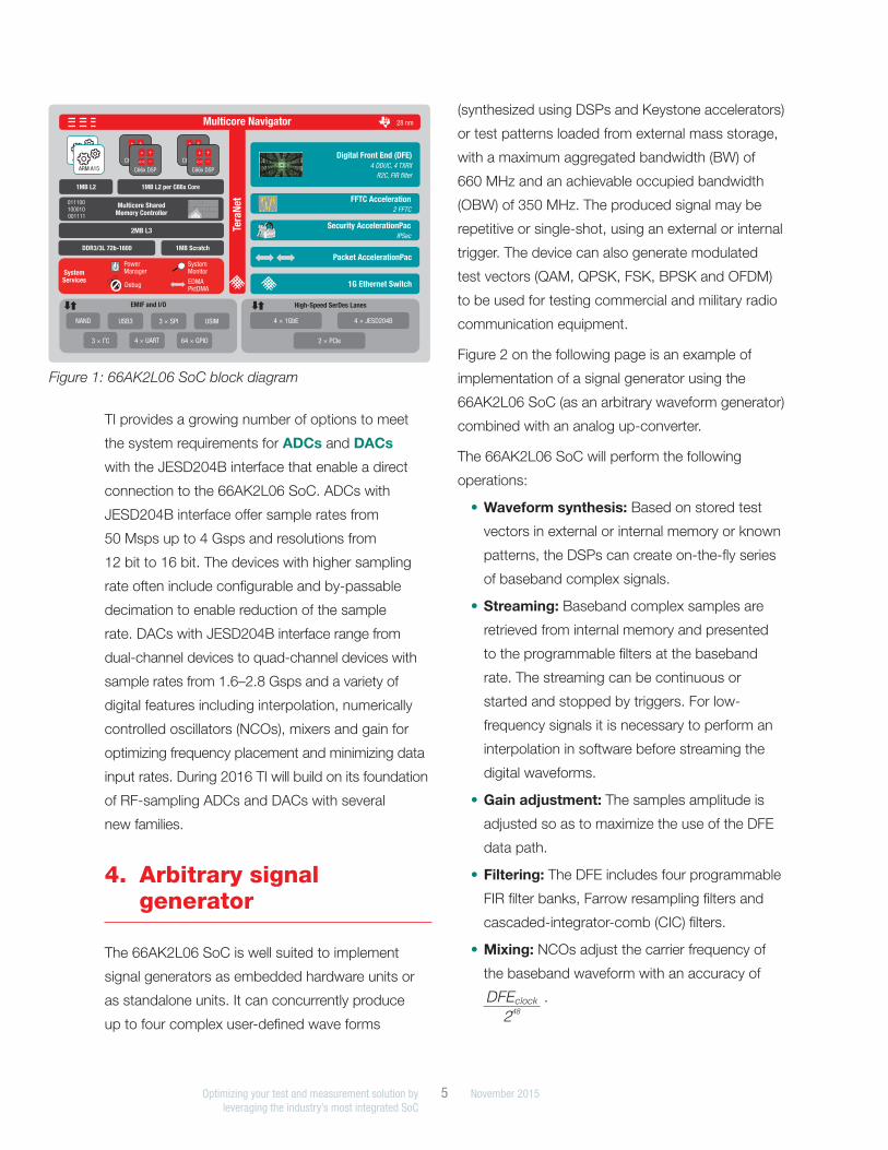
Key aspects of the KeyStone II architecture (see
Figure 1 on the following page) are the Multicore
Navigator, TeraNet and Multicore Shared Memory
Controller, leading to a highly flexible and scalable
solution for JESD204B attach applications.
66AK2L06 key features:• Two ARM Cortex-A15 RISC cores @ 1.2 GHz with
8400 DMIPS
• Four TMS320C66x DSP cores @ 1.2 GHz with fixed- and floating-point processing providing 76 GFLOPS and 153 GMACS
• Integrated DFE technology with programmable filtering, IQ imbalance correction, up and down sampling, etc. offloads heavy signal processing
• Advanced integrated network coprocessor offloads IP routing and IP termination from ARM and DSP cores
• Two Fast Fourier Transform coprocessors (FFTC) improve latency for FFT/inverse FFT (iFFT) execution up to 8K-points with better
performance than the fixed-point DSP core implementation
• Multicore Shared Memory Controller (MSMC) with 2MBytes of memory shared by the cores and the accelerators
• Multicore Navigator offers operation of single-core simplicity to multicore SoC software design
• Ethernet switch with 4× 1GbE ports
• Two single-lane PCIe Gen2 interfaces supporting up to 5 GBaud
• High-speed JESD204B chip-to-chip interface supporting up to four lanes each at 7.37 Gbps
• Compact package size: 25 mm × 25 mm FPBGA
Optimizing your test and measurement solution by 5 November 2015 leveraging the industry’s most integrated SoC
TI provides a growing number of options to meet
the system requirements for ADCs and DACs
with the JESD204B interface that enable a direct
connection to the 66AK2L06 SoC. ADCs with
JESD204B interface offer sample rates from
50 Msps up to 4 Gsps and resolutions from
12 bit to 16 bit. The devices with higher sampling
rate often include configurable and by-passable
decimation to enable reduction of the sample
rate. DACs with JESD204B interface range from
dual-channel devices to quad-channel devices with
sample rates from 1.6–2.8 Gsps and a variety of
digital features including interpolation, numerically
controlled oscillators (NCOs), mixers and gain for
optimizing frequency placement and minimizing data
input rates. During 2016 TI will build on its foundation
of RF-sampling ADCs and DACs with several
new families.
4. Arbitrary signal generator
The 66AK2L06 SoC is well suited to implement
signal generators as embedded hardware units or
as standalone units. It can concurrently produce
up to four complex user-defined wave forms
(synthesized using DSPs and Keystone accelerators)
or test patterns loaded from external mass storage,
with a maximum aggregated bandwidth (BW) of
660 MHz and an achievable occupied bandwidth
(OBW) of 350 MHz. The produced signal may be
repetitive or single-shot, using an external or internal
trigger. The device can also generate modulated
test vectors (QAM, QPSK, FSK, BPSK and OFDM)
to be used for testing commercial and military radio
communication equipment.
Figure 2 on the following page is an example of
implementation of a signal generator using the
66AK2L06 SoC (as an arbitrary waveform generator)
combined with an analog up-converter.
The 66AK2L06 SoC will perform the following
operations:
• Waveform synthesis: Based on stored test
vectors in external or internal memory or known
patterns, the DSPs can create on-the-fly series
of baseband complex signals.
• Streaming: Baseband complex samples are
retrieved from internal memory and presented
to the programmable filters at the baseband
rate. The streaming can be continuous or
started and stopped by triggers. For low-
frequency signals it is necessary to perform an
interpolation in software before streaming the
digital waveforms.
• Gain adjustment: The samples amplitude is
adjusted so as to maximize the use of the DFE
data path.
• Filtering: The DFE includes four programmable
FIR filter banks, Farrow resampling filters and
cascaded-integrator-comb (CIC) filters.
• Mixing: NCOs adjust the carrier frequency of
the baseband waveform with an accuracy of
DFEclock
248
.
High-Speed SerDes Lanes
2 × PCIe
4 × JESD204B4 × 1GbE
Multicore Shared
Memor Controller
FFTC Acceleration
2 FFTC
C66x DSP
<<
+
–
*
C66x DSP
<<
+
–
*C66x DSP
<<
+
–
*
C66x DSP
<<
+
–
*ARM A15
ARM A15
1MB L2
1MB Scratch
1MB L2 per C66x Core
28 nmMulticore Navigator
Multicore SharedMemory Controller
011100
100010
001111
EMIF and I/O
3 × I C2
4 × UART 64 × GPIO
NAND USB3 3 × SPI USIM
Tera
Net
2MB L3
DDR3/3L 72b-1600
SystemServices
PowerManager
SystemMonitor
EDMAPktDMA
Debug 1G Ethernet Switch
Packet AccelerationPac
Security AccelerationPac
IPSec
Digital Front End (DFE)
4 DDUC, 4 TXRX
R2C, FIR filter
Figure 1: 66AK2L06 SoC block diagram
Optimizing your test and measurement solution by 6 November 2015 leveraging the industry’s most integrated SoC
• Combining: Depending on the BW of the
different waveforms, the DFE can combine up
to 12 together in the same output stream. The
DFE can create four composite streams.
• Optional analog impairment correction:
Such as IQ distortion correction.
The digital/analog up-converter chain contains a
cluster of DACs which may also include interpolation
filter, some analog mixers, filters and amplifiers.
A large variety of DACs and AFEs from Texas
Instruments support JESD204B subclasses
0 and 1. They can connect to the 66AK2L06
SoC, supporting wide spectrum-span or narrow
spectrum-span signal generation. Table 1 displays
some examples of synthesis configurations that the
66AK2L06 SoC can support. It is worth noting that
the device storage capability in size and throughput
allows for the generation of long multichannel
waveform patterns. The performance of the
66AK2L06 SoC DDR interface enables real-time use
of the patterns, even for the highest signal BW.
Table 1: Signal generator use case examples
66AK2L06
C66x
C66x
C66x
C66x
4×1 MB L2
MSMC + 2 MB L3
Digital Front End
Network CoProcessor
TRX DDUC
1 GbE
PA
SA
USIM 3× SPI
4× UART
64 GPIO
NAND
2× PCIe USB 3× I C2
FFTC
FFTC
GigE
Switch
1 GbE
1 GbE
1 GbE
DDUC
DDUC
DDUC
FIR
filters
TRX
TRX
TRX
4×
JE
SD
204B
Navig
ato
r
72b DDR3 1600 1 MB Scratch
1 MB L2
A15
A15
DAC
Figure 2: Arbitrary signal generator diagram
DUC in DFE DUC in DFE/DSP*Composite analog signal bandwidth 737.28 MHz 368.64 MHz 184.32 MHz 92.16 MHz 92.16 MHz
Maximum number of composite analog channels 1 1 2 4 4
Composite signal sample rate 737.28 Msps 368.64 Msps 184.32 Msps 92.16 Msps 92.16 Msps
Number of digital channels per composite analog signal 1–12 1–12 1–12 1–12 1
Interpolation 1–192 1–192 1–192 1–192 1024
Effective bandwidth of a digital channel 3.07 MHz – 589.82 MHz 1.54 MHz – 294.91 MHz 1.54 MHz – 147.46 MHz 1.54 MHz – 73.73 MHz 0.29 MHz
Sample resolution 2× 16 bits 2× 16 bits 2× 16 bits 2× 16 bits 2× 16 bits
Total pattern length in DDR memory (sec) 0.46 s–87.38 s 0.91 s–174.76 s 1.82 s–174.76 s 3.64 s–174.76 s 932.07 s
Total pattern length in DDR memory (Msamples) 256
* An 8× interpolation filter is executed on a DSP core, then the DFE-DUC performs a 128× interpolation.

Optimizing your test and measurement solution by 7 November 2015 leveraging the industry’s most integrated SoC
Waveform synthesis
Arbitrary waveforms or test vectors can easily be
generated on 66AK2L06 and TCI6630K2L SoCs
using the optimized signal-processing libraries
for both SoCs and the radio communication
accelerators for the TCI6630K2L SoC. DSPLib
provides optimized correlation, convolution, filtering
and vector operations for 16b and 32b signals. For
example, applying a FIR filter on a complex vector
(1×1024) takes around 1.13 cycles per tap per
sample (i.e., 15.4 microsec for a 16-tap filter on a
single 1.2-GHz DSP core). If multiple waveforms are
combined in the same composite signal, the same
band sampling rate shall be used to form the digital
channels associated to the waveforms.
Streaming
Packets of baseband samples associated with
multiple digital channels are retrieved by the DFE
baseband interface from internal memory (MSMC)
or external memory (DDR) and streamed to the filter
banks. The 66AK2L06 SoC can stream up to 32
digital channels simultaneously.
Gain, mixing and combining
Depending on the configuration, each DUC filter
block can process up to 12 digital channels
simultaneously. The DDUC block in the DFE
supports:
• Gain, phase and delay adjustment of the digital
channels (pre- or post-filtering).
• Interpolation of the digital channels.
Interpolation is used to adapt the sampling
rate to the frequency span required by the
application. Programmable filtering is used to
meet the spectral emission requirements of the
synthesized signals.
• Up conversion of digital channels. The NCO
frequency is either static or varies under the
control of the DSP through the Radio Frequency
Software Developer Kit (RFSDK). The latter
option enables the synthesis of swept signals
(within a 660-MHz span).
Power meters can be used to monitor the power
of each of the digital channels separately. Up
converted digital channels are optionally aggregated
in the same composite signal. The DFE can create
four separate composite signals. The frequency
span of the composite signals is limited by their
allocated BW on the JESD204B interface as
described in the examples in Table 1 on the
previous page.
Impairment correction
Analog components suffer from impairments such
as IQ imbalance and non-linear distortion. For
instance, an analog quadrature modulator cannot
have identical amplitude on its three branches,
nor can its 90° phase shifter be perfect across the
total band of the signal. This may have an adverse
effect on the quality of the measurements in a test
environment, as measurement equipment generally
assumes that the transmitter equipment is free from
impairments. While some of the impairments may
be corrected in the measurement equipment an
alternative strategy would be to correct them in the
generator.
The 66AK2L06 SoC includes back-end automatic
gain control that helps optimize the use of the data
converter’s range and programmable FIR filters
(PFIR) that can be used to optimize either the
in-channel performance (thus reducing EVM) or out-
of-band performance (thus reducing ACPR). RFSDK
software provides a selection of predefined filters
with an optimized EVM/ACPR trade-off for LTE and
W-CDMA performance. It also allows the user to
define its own filter.

Optimizing your test and measurement solution by 8 November 2015 leveraging the industry’s most integrated SoC
More advanced corrections may be implemented
by using the capability of the 66AK2L06 or
TCI6630K2L SoCs to process simultaneously signal
synthesis (“TX path”) and signal measurements
(“feedback path”). The synthesized signal can be
pre-compensated for the impairment based on a
real-time adaptation (blind or calibrated) algorithm
executed on a DSP core. The TCI6630K2L SoC
enables the necessary feedback path.
Power estimation on the 66AK2L06 SoC
The 66AK2L06 SoC provides multiple ways of
monitoring the power of synthesized or received
signals. The DFE includes 16 flexible power
meters that can be configured to measure the
power of streaming signals at difference stages
of the processing. For signal synthesizers, the
DFE can monitor the power of the digital channel
components (up to 18 bits range) before and after
gain/filtering/interpolating. It can also monitor
the power of the digital composite signal after
optional combination of the digital channels before
and after filtering. For SAs, the DFE can monitor
the power of the received signals (up to 24 bits
range) and the power of sub-channels after gain/
filtering/decimation. The power meters may be
used in single-shot mode acting on a trigger or in
continuous mode with configurable RMS/Averaging
schemes, as well as min/max recording. A software
API in RFSDK sets up the power meters and
another API reads the power meter values. Control
of the measurement sequence in continuous
mode is automated through timers and counters.
Watermarks may be used on power meters to
trigger further processing. For example, advanced
spectrum analysis may be triggered on reception
of a transient signal. DSPLib also provides a set
of C66x optimized functions operating on real or
complex signals in support of more advanced
power analysis.
5. Arbitrary spectrum analyzer
The 66AK2L06 SoC is well suited for implementing
spectrum analyzer functions. It provides a
compact and low-power implementation due to
its JESD204B interface that enables a serialized
direct connection to the ADC and contains enough
processing, filtering and FFT resources to implement
the three most common types of spectrum
analyzers: the swept tunable SA, the vector SA and
the real-time analyzer.
The swept tunable SA is the traditional SA
architecture that has been in use for decades.
Originally implemented with purely analog
components, swept tunable SAs now also contain
an ADC and some digital signal processing.
It is designed to make frequency vs. power
measurements over a wide signal BW by down
converting the signal and sweeping it through the
passband of a resolution BW filter. The benefit of
a swept tunable SA is the large signal BW it can
handle in combination with its high dynamic range.
The fact that it is sweeping through the BW means it
can only calculate the power level at one frequency
point at a time and therefore works best in a
relatively stable input signal environment.
The vector SA does not only measure the power
level but also adds the phase information in order
to enable modulation measurements of digitally
modulated signals. The VSA digitizes the IF-signal
and performs the down conversion, filtering and
detection in the digital domain. Transformation
from time to frequency domain is done using FFT
processing.

Optimizing your test and measurement solution by 9 November 2015 leveraging the industry’s most integrated SoC
The real-time SA performs frequency vs. power
and phase measurements. It can display the time
domain data and provides seamless signal capture.
This enables real-time triggering and time-correlated
multi-dimensional measurements that enable
detection of dis-continuous signal problems such as
glitches, transients, burst transmissions and other
dynamic or intermittent phenomena.
This section will focus on how the 66AK2L06 SoC
can handle the requirements of a real-time SA since
it is the most demanding of the three applications
from a digital processing standpoint and is able to
emulate the functions of the other two types.
Figure 3 below is a generic block diagram of a real-
time SA using the 66AK2L06 SoC.
The AFE of the RTSA can be tuned across the
full frequency range of the instrument and down
converts the input signal to a fixed IF signal
matching the BW of the real time SA. The IF-signal
is filtered and digitized before being sent to the
SoC over the JESD204B interface. The signal is
further down converted and processed in time and
frequency domains within the SoC before results
are presented.
Signal processing
The 66AK2L06 SoC can support digital signal
processing techniques used in spectrum analysis,
applied to samples, frames or blocks of data.
• Sample level processing:
• DDUC accelerators in DFE support filtering of
the captured samples. Variable band low-
pass filtering can be used to reject part of the
incoming signal or to shape it.
• DDUC blocks in DFE support down
conversion of the captured samples and
support decimation of the captured samples
(I/Q pairs). Decimation is used to adapt the
sampling rate to the frequency span required
by the user.
• Frame level processing
• FFTC accelerators support FFT, iFFT, DFT and
iDFT.
• DSPLib provides a large variety of optimized
fixed- and floating-point FFTs and DFT C66x
routines for real or complex data.
66AK2L06
C66x
C66x
C66x
C66x
4×1 MB L2
MSMC + 2 MB L3
Digital Front End
Network CoProcessor
TRX DDUC
1 GbE
PA
SA
USIM 3× SPI
4× UART
64 GPIO
NAND
2× PCIe USB 3× I C2
FFTC
FFTC
GigE
Switch
1 GbE
1 GbE
1 GbE
DDUC
DDUC
DDUC
FIR
filters
TRX
TRX
TRX
4×
JE
SD
204B
Navig
ato
r
72b DDR3 1600 1 MB Scratch
1 MB L2
A15
A15
ADC
IF filter
Low-pass filter
Mixer
Attenuator
DDR3
Figure 3: Generic block diagram of a real-time spectrum analyzer

Optimizing your test and measurement solution by 10 November 2015 leveraging the industry’s most integrated SoC
• Block level processing
• DSPLib provides optimized vector
multiplication routines to implement
smoothing spectrogram windows.
• The Multi-Core Software Developer Kit
(MCSDK) supports the manipulation of large
blocks of data in overlapping spectrograms.
• DSPLib provides a large variety of filtering,
correlation and convolution routines to be
used in multi-domain analysis.
Table 2 below presents the performance to expect
from the 66AK2L06 SoC depending on the
implementation of the Fast Fourier Transform (16b
fixed-point I/Q on FFTC, 16b fixed-point I/Q on
C66x, floating point (FP) on C66x).
Leveraging the DDC and the filtering in the DFE
block in conjunction with the FFT performance
of the FFTC and the C66x cores, the 66AK2L06
SoC can support a wide range of SA use cases.
The digital down converter in the DFE block has a
maximum down conversion ratio of 192. If a higher
ratio is required, the DFE limitation can be overcome
by leveraging the device DMA infrastructure, as
long as the DFE DDC filter is set to meet Nyquist
limit for the total decimation. Instead of passing all
samples from the DFE to the FFTC, the DMA engine
passes one out of two, four or eight samples. This
will increase the maximum decimation to 1,536.
If further decimation is needed it can easily be
implemented using one of the C66x DSP cores and
the appropriate optimized functions from DSPLib.
Table 3 on the following page includes a few
examples of SA use cases. The example on the far
right is using the DSP for down conversion.
The indicated sample rate assumes complex data
so 368 Msps corresponds to 736 Msps for real
data. This is currently the upper limit of what the
66AK2L06 SoC DFE block is able to support and
requires a speed of 7.3 Gbps over two lanes on the
JESD204B interface. Future enhancements include
running the DFE at higher clock speeds and thus
higher sampling rates.
All of the examples in Table 3 on the following page
may use continuous acquisition storing the data in
DDR memory configured as a FIFO. The highest
rate accounts for no more than 12 percent of the
DDR BW capacity. This enables real-time triggers
to be implemented in the DSP. Once triggered, the
data acquisition can either be stopped immediately
or can continue to run for a configurable amount of
time to store enough data to enable analysis both
before and after the trigger point.
Table 2: FFT performance table
FFT size 16 32 64 128 256 512 1024 2048 4096 8192
SNR
(dB)
16b I/Q on FFTC 91.1 89.3 88.4 86.2 87.5 85.5 85.2 84.8 84.1 83.8
16b I/Q on C66x 72.2 69.1 69 67.1 67 65.7 65.6 64.6 64.5 63.7
FP on C66x ~300 dB
FFTs
/s
16b I/Q on one FFTC 22.86M 12.97M 9.80M 4.95M 2.98M 1.33M 705k 303k 154k 66k
16b I/Q on one C66x 175k 75k 36k 9k
FP on one C66x 74k 35k 9k 4k
GFLO
PS 16b I/Q on FFTC 7.3 10.4 18.8 22.2 30.5 30.6 36.1 34.1 37.8 35.4
16b I/Q on C66x 9.0 8.4 8.9 5
FFT performance measured in GFLOPS uses the following complex transform formula where T is the time (in ns) to execute one FFT and N is the FFT size
GFLOPS =5 logN N
T
2

Optimizing your test and measurement solution by 11 November 2015 leveraging the industry’s most integrated SoC
In order to avoid spectrum leakage caused
by discontinuities between the FFT frames, a
combination of windowing and overlapping
FFT frames can be applied. The windowing
deemphasizes the samples close to the edge of the
FFT frame where the artificial spurious responses
would occur while the overlapping FFT frames will
ensure that spectral events close to the fame edge
are not lost due to the windowing. The windowing
can be implemented by post-processing the results
of the FFTC, using DSP cores and optimized library
functions. The two FFTC accelerators are able to
fully offload all of the FFT processing including the
use of overlapping FFT frames, reserving the use of
the DSP resources for advanced signal processing
tasks. The Packet DMA engine solves the intense
internal data management by moving data between
memory-mapped locations without any processor
intervention. A descriptor, associated to every
block of data, identifies the source and destination
address for the move, as well as the data structure.
The descriptors are generated by the processing
cores or by the peripherals. They are distributed
in hardware queues managed by the Multicore
Navigator.
Another function that could be offloaded to the DFE
block is the IQ-imbalance correction that would
be implemented using logic within the JESD204B
receiver block. Correction parameters are estimated
either based of complex gain imbalance correction
information from the JESD204B block or based on
a single-tap blind estimation algorithm. This function
would be useful when a zero IF complex stream is
input to the RX sub-block.
Triggers
The 66AK2L06 SoC enables flexible triggers of
different types to be implemented. The triggers can
be used to either start or stop data acquisition.
These can be split into two main categories.
1. External triggers can trigger through a transition
on one of the 64 GPIOs or through messaging
DDC in DFE DDC in DSPSuper side span Wide span Medium span Medium span Narrow span Narrow span
Spectrum bandwidth 330 MHz 20 MHz 1 MHz 1 MHz 1 kHz 1 kHz
Sample rate 368 Msps 368 Msps 368 Msps 368 Msps 368 Msps 368 Msps
Decimation 1 12 128 128 1536* 131072
Effective sample rate 368 Msps 31 Msps 3 Msps 3 Msps 240 ksps 3 ksps
Time domain resolution (sample) 2.72 ns 32.61 ns 347.83 ns 347.83 ns 4.17 µs 356.17 µs
FFT size 8196 8196 8196 1024 8196 2048
Spectrogram time resolution (frame length) 22 µs 267 µs 2851 µs 356 µs 34 ms 729 ms
Sample size 32 bits 32 bits 32 bits 32 bits 32 bits 32 bits
Maximum record length with MSMC (2 MB memory) 178 µs 2137 µs 23 ms 23 ns 274 ms 23342 ms
Maximum record length with DDR (8 GB memory) 729 ms 8.75 s 93 s 93 s 1120 s 26.6 h
Frequency resolution (FFT bin width) 44.9 kHz 3.7 kHz 0.35 kHz 2.8 kHz 29.2 Hz 1.4 Hz
* Decimation achieved by a combination of DDC and DMA.
Table 3: Spectrum analyzer example use cases for a single channel

Optimizing your test and measurement solution by 12 November 2015 leveraging the industry’s most integrated SoC
passed through one of the complex I/Os
including PCIe, Ethernet, I2C, SPI, UART, USB
or the JESD204B.
2. Internal triggers are generated by the cores or
by signal-processing accelerators. One of the
most interesting families of internal triggers is
generated by the DFE. While processing the
data from the ADC, it can generate a trigger
based on the characteristics of incoming data.
Examples of internal triggers include:
• Power based DFE triggers: These can
be based on the power level of the digitized
signal from the ADC before filtering and
decimation looking at the full spectrum or the
power level after filtering and decimation. The
DFE block has a number of built-in power
meters that can provide power measurements
before and after DDC and filtering.
• Software-based frequency triggers: A
frequency-based trigger can be implemented
in software using the C66x DSPs and is
therefore very flexible. The DSPs are able to
post-process all the results from the FFTCs
enabling complex frequency masks to trigger
on specific power levels being above or below
the defined threshold in selected parts of
the spectrum. To enable the analysis in real
time, the packet DMA engine is used for all
internal DMA traffic between the DSP cores
and the FFTC, offloading the DSP cores and
minimizing stalls.
As the trigger analysis runs in real time, software-
defined timers can be used to detail how much
data shall be stored in DDR before and after the
trigger point to enable the user to do analysis of
the spectrum both before and after the trigger
occurred.
6. I/O connectivity
In addition to greater integration at the silicon level,
the 66AK2L06 SoC enables a small bill of materials
(BOM), reducing board production costs through
the use of high-performance serial interfaces such
as JESD204B, PCIe, 1 GbE, USB and SPI. They
simplify circuit board design and layout, and enable
a vast number of ways to connect and present the
analyzed data. See Figure 4 on the following page.
USB
The USB interface is a general-purpose cable-
bus supporting data exchange between a host
and several peripherals. It can interface with a
PC or a graphics processor such as TI Sitara™
processors. The interface can also be used as a
hard drive port for mass storage.
The 66AK2L06 SoC has two bidirectional USB
lanes. Each lane supports Full/High/Super-speed
modes in both directions in both peripheral and
host mode. When in host mode, the Low speed
mode is also supported. The controller is backward
compatible with USB 2.0. All software drivers
needed for the USB interface are available through
the MCSDK.[2]
1 GbE
The 66AK2L06 SoC has a five-port (four external)
gigabit Ethernet switch for 802.3-compliant Ethernet
traffic. The four external ports are independent
SGMII modules that can be configured individually.
The 66AK2L06 SoC can also implement a
Linux®-based web server to enable remote control.
A web server is available in the RFSDK for the
control and operation of the DFE subsystem.
The Network Coprocessor – (NetCP) resides
behind the gigabit Ethernet switch and implements

Optimizing your test and measurement solution by 13 November 2015 leveraging the industry’s most integrated SoC
a packet accelerator (PA) for header processing
such as header matching and CRC generation, a
security accelerator for encryption and decryption
operations and a packet DMA controller for internal
packet communication.
The NetCP is able to handle up to 1500 kpps. The
PA supports ingress features like L3 reassembly,
access control list (ACL) processing and multi-
route processing, on egress IP-fragmentation,
L2 framing and L4 checksum is supported. The
security accelerator supports up to 6.4 Gbps of
encryption and decryption for IPSEC (IKE, AH, ESP,
SRTP), 3GPP and others. Other functions include
true random number generation and public key
accelerator. All low-level drivers (LLD) needed to
drive the NetCP are available in the NetLib software
that is part of the MCSDK.[2]
PCIe
The PCIExpress (PCIe) module is a high-speed
serial interface that provides a reliable general-
purpose connection primarily used over PCB or
backplane to connect to other PCIe-compliant
devices. Each lane can be operated with a raw bit
rate up to 5.0 Gbps. All software drivers needed for
the PCIe interface are available through the MCSDK.
For more information on the PCIe interface see [2].
An extension to the PCIe interface commonly used
within automated test systems is PCI Express
eXtensions for Instrumentation (PXI Express). PXI
and PXI Express are industry standards governed
by the PXI Systems Alliance (PXISA) and provide a
cheap, robust and high-speed interface based on
standard PCI/PCIe interfaces. On top of the PCI/
PCIe interface, timing and synchronization features
have been added to enable accurate remote control
66AK2L06
C66x
C66x
C66x
C66x
4×1 MB L2
MSMC + 2 MB L3
Digital Front End
Network CoProcessor
TRX DDUC
1 GbE
PA
SA
USIM 3× SPI
4× UART
64 GPIO
NAND
2× PCIe USB 3× I C2
FFTC
FFTC
GigE
Switch
1 GbE
1 GbE
1 GbE
DDUC
DDUC
DDUC
FIR
filters
TRX
TRX
TRX
4×
JE
SD
204B
Navig
ato
r
72b DDR3 1600 1 MB Scratch
1 MB L2
A15
A15
DDR3
High-Speed
Data Converter
High-Speed
Data Converter
SitaraProcessor
™
Figure 4: 66AK2L06 I/O connection options

Optimizing your test and measurement solution by 14 November 2015 leveraging the industry’s most integrated SoC
of the measurement system. The 66AK2L06 SoC
supports PCIe and with buffered GPIO signals can
also be used to enable a PXIe board design.
SPI
The Serial Peripheral Interconnect (SPI) port is a
synchronous serial input/output port that allows a bit
stream of programmable length to be shifted in/out [2]. The main intent behind the SPI port is to provide
a connection to a SPI ROM for boot. The 66AK2L06
SoC has three SPI ports that can operate at speeds
up to 66 MHz. All necessary drivers for the interface
are part of the MCSDK.
JESD204B
JESD204B provides a high-throughput, low-pin-
count serial link between ADCs, DACs, DSPs,
SoCs, field programmable gate arrays (FPGAs) and
application-specific integrated circuits (ASIC). The
interface enables a low-power implementation with
reduced board space and complexity compared to
traditional CMOS or LVDS implementations. More
information on the benefits of JESD204B can be
found in [5].
The JESD204B interface on the 66AK2L06 SoC
consists of four bidirectional SERDES lanes
operating at rates up to 7.3 Gbps. It connects
directly to the DFE block. The DFE uses the lanes
separately or combined to transport one, two or
four data streams in each direction. The DFE can
split or aggregate up to 12 digital channels on
each of the data streams. The interface supports
JESD204B subclass 0 for backward compatibility
with JESD204A and subclass 1 that supports
deterministic latency. See Figure 5.
7. 66AK2L06 SoC development environment
Besides providing powerful hardware resources,
the 66AK2L06 SoC comes with a rich set of
development tools and libraries, that can kick-start
a design, shorten the overall development time and
sustain upgrades throughout the life of the product.
An evaluation module and reference design is also
available.
• 66AK2L06 Evaluation Module – The
66AK2L06 SoC evaluation module with the
JESD204B interfaces rooted to an FMC
connector. This module connects seamlessly to
TI DACs and ADC evaluation modules.[6]
• TI Design TIDEP0034 – a reference design
connecting TI’s ADC12J4000 and DAC38J84
to the 66AK2L06 SoC through the JESD204B
interface. For more information see [4].
• Code Composer Studio™ Integrated
Development Environment (IDE) provides an
integrated development environment supporting
all TI processor platforms and is used to
develop and debug embedded applications.
It consists of a suite of tools including C/C++
compiler, source code editor, project build
environment, debugger, profiler, libraries and
many other features.
Maximum
lane rate
Synchronization with
deterministic latency
Lower pin
counts
Simplifies layout with
fewer interconnects
JESD204BADC
DAC
ADC
DAC
66AK2L06
SoC
JESD204B
Reduces design complexity,
board space and cost
Figure 5: JESD interface benefits

Optimizing your test and measurement solution by 15 November 2015 leveraging the industry’s most integrated SoC
• MCSDK – Provides foundational software for
TI ARM and DSP-based devices. It includes
components like:
• SYS/BIOS real-time embedded operating
system on DSP cores
• Linux high-level operating system running on
ARM processors (SMP mode for multicore
ARM processors)
• DSP chip support libraries, DSP/ARM drivers,
and basic platform utilities
• Inter-processor communication across cores
and devices
• SoC resource management
• Trace debug and instrumentation
• Bootloaders and boot utilities, power-on self-
test
• Latest toolchain (Linaro, DSP TI CodeGen)
• Host tools, integrated development
environment
• DSPLib – The library, delivered in source as
part of Code Composer Studio IDE, contains
a large portfolio of digital signal processing
functions used as building blocks in various
applications. These routines are highly
optimized utilizing all the features of the C66x
core and include both fixed- and floating-point
kernels. DSPLib includes following functions:
• Adaptive filtering
• Correlation
• Fast Fourier Transform
• Filtering and convolution
• Matrix computations
• RFSDK – Contains a set of APIs that are used
to setup and control the DFE block inside the
66AK2L06 SoC, the JESD204B interface and
also any ADC, DAC or AFE connected to the
JESD interface.
• NetLib/TransportNetLib, delivered as a part
of the MCSDK, consists of a software package
for ARM user space applications to gain
access to NetCP. The NetLib includes two main
software components, the High-Performance
Lib (HPLIB) and Network API (NetAPI) modules.
The HPLIB is a low-overhead library optimized
for fast path applications (user plane, UDP/IP)
while the NetAPI contains send/receive APIs
along with data path configurations (control
plane, GTP/IP).
8. Conclusion
Based on TI’s high-throughput KeyStone II
architecture, the 66AK2L06 SoC is a scalable, low-
power solution with a superior processing system
including integrated FFT hardware acceleration,
DFE, high-speed JESD204B interface and a
network coprocessor with an integrated GBE
switch.
The platform offers FFT performance, using the
FFTCs and C66x DSP cores, up to 46 MFFT/s
with an SNR that ranges from 84 dB (fixed point)
to 300 dB (floating point). The JESD204B interface
provides a high-speed, low-power connection
directly to the analog front end or data converters.
The C66x cores together with the rich set of
provided signal-processing source code libraries
bring efficient signal-processing capacity, while the
ARM Cortex-A15 cores provide access to a large
set of Linux-based and open-source libraries and
services. These features together with the rich set
of I/Os makes it an excellent SoC platform for the
demanding requirements of the T&M market including
SWaP-C, time to market and future proof-ness.
This device offers designers of T&M applications a
single hardware and software platform to address
SPRY293© 2015 Texas Instruments Incorporated
Important Notice: The products and services of Texas Instruments Incorporated and its subsidiaries described herein are sold subject to TI’s standard terms and conditions of sale. Customers are advised to obtain the most current and complete information about TI products and services before placing orders. TI assumes no liability for applications assistance, customer’s applications or product designs, software performance, or infringement of patents. The publication of information regarding any other company’s products or services does not constitute TI’s approval, warranty or endorsement thereof.
The platform bar, Code Composer Studio, KeyStone and Sitara are trademarks of Texas Instruments. All trademarks are the property of their respective owners.
a variety of applications for signal generation and
signal analysis. It enables differentiated features with
product lifetime upgrades as well as field upgrades.
Designers can get started today with the 66AK2L06
SoC and TI high-speed data converters on the
evaluation module.[4]
References
[1] Hardik Gandhi, Debbie Greenstreet, Joe Quintal
Digital, Texas Instruments white paper “Radio
Front-End strategies provide game-changing
benefits for small cell base stations”.
[2] 66AK2L06 technical documents
[3] TCI6630K2L SoC, High-performance, low-
power solution for indoor enterprise PoE+
small cells and outdoor pico deployments.
[4] 66AK2L06 DSP+ARM SoC JESD204B Attach
to Wideband ADCs and DACs TI Reference
Design
[5] Ready to make the jump to JESD204B?
[6] 66AK2L06 Evaluation Module

IMPORTANT NOTICE
Texas Instruments Incorporated and its subsidiaries (TI) reserve the right to make corrections, enhancements, improvements and otherchanges to its semiconductor products and services per JESD46, latest issue, and to discontinue any product or service per JESD48, latestissue. Buyers should obtain the latest relevant information before placing orders and should verify that such information is current andcomplete. All semiconductor products (also referred to herein as “components”) are sold subject to TI’s terms and conditions of salesupplied at the time of order acknowledgment.TI warrants performance of its components to the specifications applicable at the time of sale, in accordance with the warranty in TI’s termsand conditions of sale of semiconductor products. Testing and other quality control techniques are used to the extent TI deems necessaryto support this warranty. Except where mandated by applicable law, testing of all parameters of each component is not necessarilyperformed.TI assumes no liability for applications assistance or the design of Buyers’ products. Buyers are responsible for their products andapplications using TI components. To minimize the risks associated with Buyers’ products and applications, Buyers should provideadequate design and operating safeguards.TI does not warrant or represent that any license, either express or implied, is granted under any patent right, copyright, mask work right, orother intellectual property right relating to any combination, machine, or process in which TI components or services are used. Informationpublished by TI regarding third-party products or services does not constitute a license to use such products or services or a warranty orendorsement thereof. Use of such information may require a license from a third party under the patents or other intellectual property of thethird party, or a license from TI under the patents or other intellectual property of TI.Reproduction of significant portions of TI information in TI data books or data sheets is permissible only if reproduction is without alterationand is accompanied by all associated warranties, conditions, limitations, and notices. TI is not responsible or liable for such altereddocumentation. Information of third parties may be subject to additional restrictions.Resale of TI components or services with statements different from or beyond the parameters stated by TI for that component or servicevoids all express and any implied warranties for the associated TI component or service and is an unfair and deceptive business practice.TI is not responsible or liable for any such statements.Buyer acknowledges and agrees that it is solely responsible for compliance with all legal, regulatory and safety-related requirementsconcerning its products, and any use of TI components in its applications, notwithstanding any applications-related information or supportthat may be provided by TI. Buyer represents and agrees that it has all the necessary expertise to create and implement safeguards whichanticipate dangerous consequences of failures, monitor failures and their consequences, lessen the likelihood of failures that might causeharm and take appropriate remedial actions. Buyer will fully indemnify TI and its representatives against any damages arising out of the useof any TI components in safety-critical applications.In some cases, TI components may be promoted specifically to facilitate safety-related applications. With such components, TI’s goal is tohelp enable customers to design and create their own end-product solutions that meet applicable functional safety standards andrequirements. Nonetheless, such components are subject to these terms.No TI components are authorized for use in FDA Class III (or similar life-critical medical equipment) unless authorized officers of the partieshave executed a special agreement specifically governing such use.Only those TI components which TI has specifically designated as military grade or “enhanced plastic” are designed and intended for use inmilitary/aerospace applications or environments. Buyer acknowledges and agrees that any military or aerospace use of TI componentswhich have not been so designated is solely at the Buyer's risk, and that Buyer is solely responsible for compliance with all legal andregulatory requirements in connection with such use.TI has specifically designated certain components as meeting ISO/TS16949 requirements, mainly for automotive use. In any case of use ofnon-designated products, TI will not be responsible for any failure to meet ISO/TS16949.
Products ApplicationsAudio www.ti.com/audio Automotive and Transportation www.ti.com/automotiveAmplifiers amplifier.ti.com Communications and Telecom www.ti.com/communicationsData Converters dataconverter.ti.com Computers and Peripherals www.ti.com/computersDLP® Products www.dlp.com Consumer Electronics www.ti.com/consumer-appsDSP dsp.ti.com Energy and Lighting www.ti.com/energyClocks and Timers www.ti.com/clocks Industrial www.ti.com/industrialInterface interface.ti.com Medical www.ti.com/medicalLogic logic.ti.com Security www.ti.com/securityPower Mgmt power.ti.com Space, Avionics and Defense www.ti.com/space-avionics-defenseMicrocontrollers microcontroller.ti.com Video and Imaging www.ti.com/videoRFID www.ti-rfid.comOMAP Applications Processors www.ti.com/omap TI E2E Community e2e.ti.comWireless Connectivity www.ti.com/wirelessconnectivity
Mailing Address: Texas Instruments, Post Office Box 655303, Dallas, Texas 75265Copyright © 2015, Texas Instruments Incorporated