Embed Size (px)
Citation preview
BSL316C
OptiMOS™ 2 + OptiMOS™-P 2 Small Signal Transistor
Features
· Complementary P + N channel
· Enhancement mode
· Logic level (4.5V rated)
· Avalanche rated
· Qualified according to AEC Q101
· 100% lead-free; RoHS compliant
· Halogen free according to IEC61249-2-21
Maximum ratings, at T j=25 °C, unless otherwise specified 1)
Parameter Symbol Conditions Unit
P N
Continuous drain current I D T A=25 °C -1.5 1.4 A
T A=70 °C -1.2 1.1
Pulsed drain current I D,pulse T A=25 °C -6.0 5.6
Avalanche energy, single pulse E AS
P: I D=-1.5 A,
N: I D=1.4 A,
R GS=25 W
11 3.7 mJ
Gate source voltage V GS V
Power dissipation1) P tot T A=25 °C W
Operating and storage temperature T j, T stg °C
ESD class JESD22-A114-HBM
Soldering temperature T solder °C
IEC climatic category; DIN IEC 68-1
Value
-55 ... 150
55/150/56
260
±20
0.5
1) Remark: only one of both transistors active
0 (<250V)
PG-TSOP6
Type Package Tape and Reel Information Marking Lead Free Packing
BSL316C PG-TSOP-6 H6327: 3000 pcs / reel sPJ Yes Non dry
P N
VDS -30 30 V
RDS(on),max VGS=±10 V 150 160 mW
VGS=±4.5 V 270 280
ID -1.5 1.4 A
Product Summary
4 5
6
1 2
3
Rev. 2.3 page 1 2014-07-21
BSL316C
Parameter Symbol Conditions Unit
min. typ. max.
Thermal characteristics
P
N
Electrical characteristics, at T j=25 °C, unless otherwise specified
Static characteristics
Drain-source breakdown voltage P V (BR)DSS V GS=0 V, I D=-250 µA - - -30 V
N V GS=0 V, I D=250 µA 30 - -
Gate threshold voltage P V GS(th) V DS=V GS, I D=-11 µA -2 -1.5 -1
N V DS=V GS, I D=3.7 µA 1.2 1.6 2
Zero gate voltage drain current P I DSS
V DS=-30 V, V GS=0 V,
T j=25 °C- - -1 µA
NV DS=30 V, V GS=0 V,
T j=25 °C- - 1
PV DS=-30 V, V GS=0 V,
T j=150 °C- - -100
NV DS=30 V, V GS=0 V,
T j=150 °C- - 100
Gate-source leakage current P
N
P R DS(on)
V GS=-4.5 V, I D=-
1.1 A- 177 270 mW
N V GS=4.5 V, I D=-1.1 A - 191 280
P V GS=-10 V, I D=-1.5 A - 113 150
N V GS=10 V, I D=1.4 A - 119 160
Transconductance P g fs
|V DS|>2|I D|R DS(on)max,
I D=-1.18 A- 2.7 - S
N|V DS|>2|I D|R DS(on)max,
I D=1.1 A- 2.3 -
±100
R thJA
nAI GSS -V GS=±20 V, V DS=0 V -
Values
2) Performed on 40mm
2 FR4 PCB. The traces are 1mm wide, 70μm thick and 20mm long; they are present on both
sides of the PCB
Drain-source on-state
resistance
Thermal resistance, junction -
ambient1) - - 250minimal footprint
2) K/W
Rev. 2.3 page 2 2014-07-21
BSL316C
Parameter Symbol Conditions Unit
min. typ. max.
Dynamic characteristics
Input capacitance P C iss - 212 282 pF
N - 71 94
Output capacitance P C oss - 69 91
N - 26 35
Reverse transfer capacitance P Crss - 56 84
N - 5 7
Turn-on delay time P t d(on) - 5.0 - ns
N - 3.4 -
Rise time P t r - 6.5 -
N - 2.3 -
Turn-off delay time P t d(off) - 14.3 -
N - 5.8 -
Fall time P t f - 7.5 -
N - 1.0 -
Gate Charge Characteristics
Gate to source charge P Q gs - -0.6 - nC
Gate to drain charge Q gd - -1.2 -
Switching charge Q g - -2.4 -
Gate plateau voltage V plateau - -2.9 -
Gate to source charge N Q gs - 0.3 -
Gate to drain charge Q gd - 0.2 -
Switching charge Q g 0.6 -
Gate plateau voltage V plateau - 3.4 -
V DD=15 V,
I D=1.4 A,
V GS=0 to 5 V
Values
V GS=0 V,
P: V DS=-15 V,
N: V DS= 15 V,
f =1 MHz
P: V DD=-15 V,
V GS=-10 V, R G=6 W,
I D=-1.5 A
N: V DD=15 V,
V GS=10 V, R G=6 W,
I D=1.4 A
V DD=-15 V,
I D=-1.5 A,
V GS=0 to -5 V
Rev. 2.3 page 3 2014-07-21
BSL316C
Parameter Symbol Conditions Unit
min. typ. max.
Reverse Diode
P I S - - -0.5 A
N - - 0.5
Diode pulse current P I S,pulse - - -6.0
N - - 5.6
Diode forward voltage P V SD
V GS=0 V, I F=-1.5 A,
T j=25 °C- -0.8 -1.1 V
NV GS=0 V, I F=1.4 A,
T j=25 °C- 0.86 1.1
Reverse recovery time P t rr - 8.2 - ns
N - 9.1 -
Reverse recovery charge P Q rr - 2.1 - nC
N - 2.6 -
Diode continuous forward current
Values
T C=25 °C
V R=±15 V, I F=I S,
di F/dt =100 A/µs
Rev. 2.3 page 4 2014-07-21
BSL316C
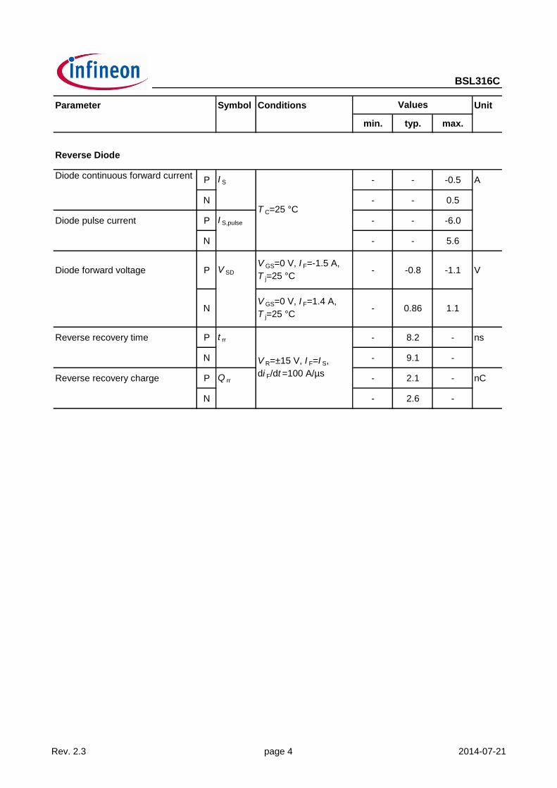
1 Power dissipation (P) 2 Power dissipation (N)
P tot=f(T A) P tot=f(T A)
3 Drain current (P) 4 Drain current (N)
I D=f(T A) I D=f(T A)
parameter: V GS≤-10 V parameter: V GS≥10 V
0
0.1
0.2
0.3
0.4
0.5
0.6
0 40 80 120 160
Pto
t [W
]
TA [°C]
0
0.2
0.4
0.6
0.8
1
1.2
1.4
1.6
0 40 80 120 160
I D [
A]
TA [°C]
0
0.1
0.2
0.3
0.4
0.5
0.6
0 40 80 120 160
Pto
t [W
]
TA [°C]
0
0.2
0.4
0.6
0.8
1
1.2
1.4
1.6
0 40 80 120 160
-ID [
A]
TA [°C]
Rev. 2.3 page 5 2014-07-21
BSL316C
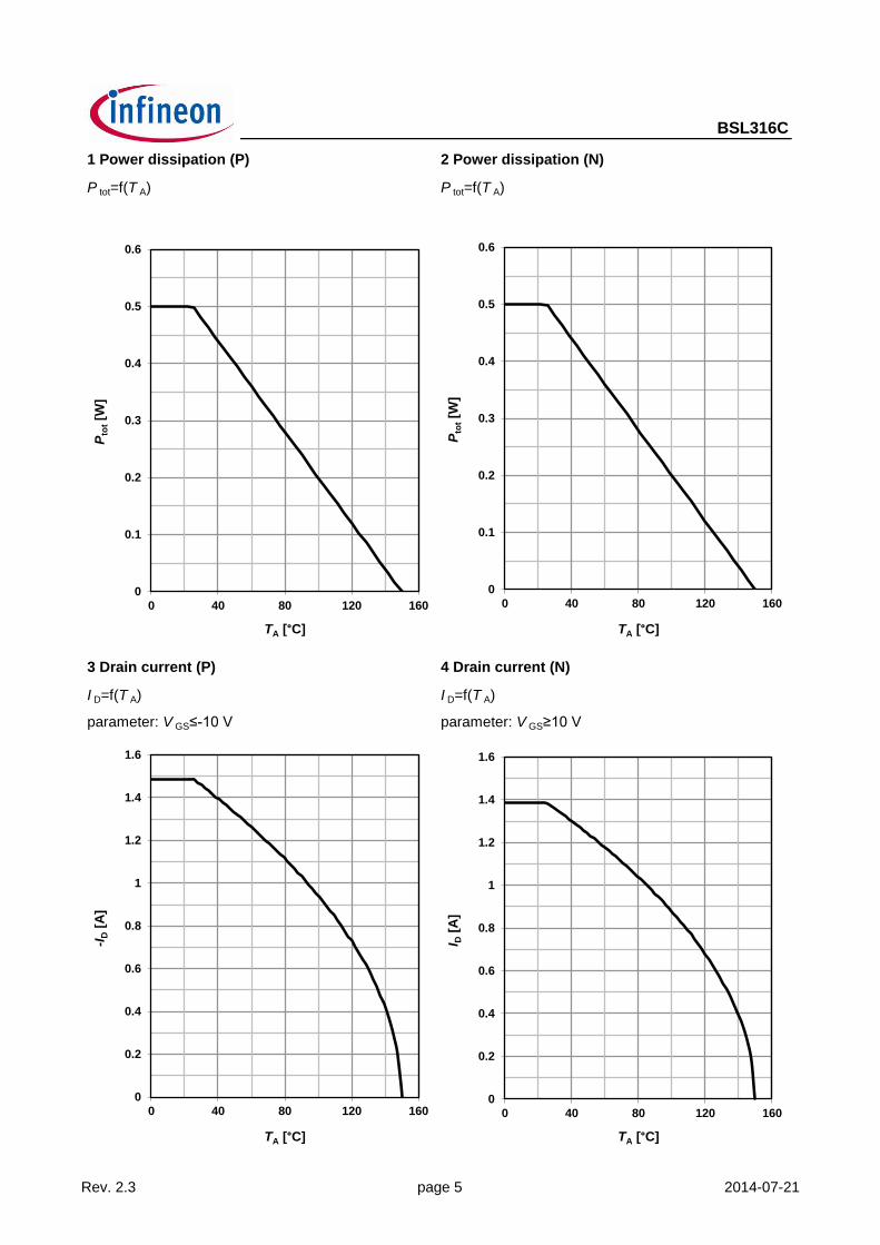
5 Safe operating area (P) 6 Safe operating area (N)
I D=f(V DS); T A=25 °C; D =0 I D=f(V DS); T A=25 °C; D =0
parameter: t p parameter: t p
7 Max. transient thermal impedance (P) 8 Max. transient thermal impedance (N)
Z thJA=f(t p) Z thJA=f(t p)
parameter: D =t p/T parameter: D =t p/T
1 µs
10 µs
100 µs
1 ms
10 ms
DC
10-1 100 101 102
10-2
10-1
100
101
I D [
A]
VDS [V]
single pulse
0.01
0.02
0.05
0.1
0.2
0.5
10-5 10-4 10-3 10-2 10-1 100 101 102
100
101
102
103
Zth
JA [
K/W
]
tp [s]
1 µs
10 µs
100 µs
1 ms
10 ms
DC
10-1 100 101 102
10-2
10-1
100
101
-ID [
A]
-VDS [V]
single pulse
0.01
0.02
0.05
0.1
0.2
0.5
10-5 10-4 10-3 10-2 10-1 100 101 102
100
101
102
103
Zth
JA [
K/W
]
tp [s]
Rev. 2.3 page 6 2014-07-21
BSL316C
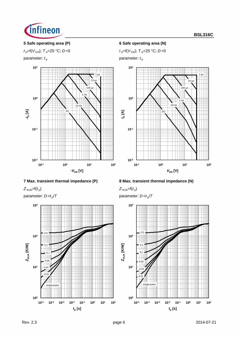
9 Typ. output characteristics (P) 10 Typ. output characteristics (N)
I D=f(V DS); T j=25 °C I D=f(V DS); T j=25 °C
parameter: V GS parameter: V GS
11 Typ. drain-source on resistance (P) 12 Typ. drain-source on resistance (N)
R DS(on)=f(I D); T j=25 °C R DS(on)=f(I D); T j=25 °C
parameter: V GS parameter: V GS
2.5 V
3 V
3.5 V
4 V
4.5 V 5 V
10 V
0
1
2
3
4
5
6
0 1 2 3
I D [
A]
VDS [V]
3.5 V
4 V
4.5 V
5 V
10 V
0
50
100
150
200
250
300
350
400
0 1 2 3 4 5
RD
S(o
n) [
mW
]
ID [A]
-2.5 V
-3 V
-3.5 V
-4 V -4.5 V -5 V -10 V
0
1
2
3
4
5
6
0 1 2 3
-ID [
A]
-VDS [V]
-3 V
-3.5 V
-4 V
-4.5 V
-5 V
-10 V
0
50
100
150
200
250
300
350
400
0 1 2 3 4 5
RD
S(o
n) [
mW
]
-ID [A]
Rev. 2.3 page 7 2014-07-21
BSL316C
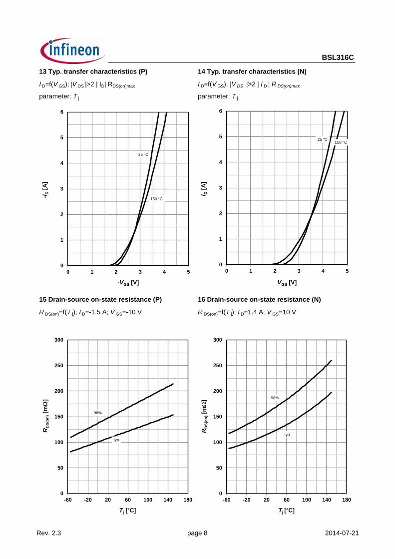
13 Typ. transfer characteristics (P) 14 Typ. transfer characteristics (N)
I D=f(V GS); |V DS |>2 | ID| RDS(on)max I D=f(V GS); |V DS |>2 | I D | R DS(on)max
parameter: T j parameter: T j
15 Drain-source on-state resistance (P) 16 Drain-source on-state resistance (N)
R DS(on)=f(T j); I D=-1.5 A; V GS=-10 V R DS(on)=f(T j); I D=1.4 A; V GS=10 V
25 °C 150 °C
0
1
2
3
4
5
6
0 1 2 3 4 5
I D [
A]
VGS [V]
25 °C
150 °C
0
1
2
3
4
5
6
0 1 2 3 4 5
-ID [
A]
-VGS [V]
typ
98%
0
50
100
150
200
250
300
-60 -20 20 60 100 140 180
RD
S(o
n) [m
W]
Tj [°C]
typ
98%
0
50
100
150
200
250
300
-60 -20 20 60 100 140 180
RD
S(o
n) [m
W]
Tj [°C]
Rev. 2.3 page 8 2014-07-21
BSL316C
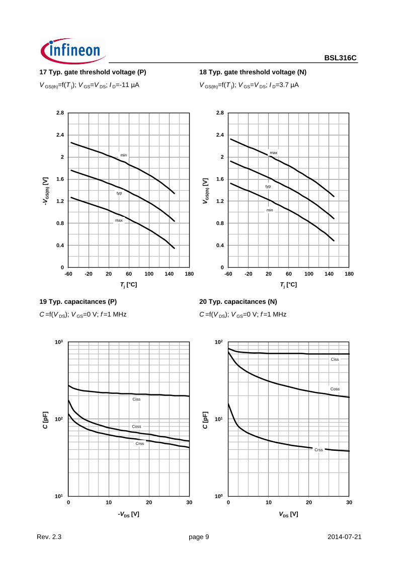
17 Typ. gate threshold voltage (P) 18 Typ. gate threshold voltage (N)
V GS(th)=f(T j); V GS=V DS; I D=-11 µA V GS(th)=f(T j); V GS=V DS; I D=3.7 µA
19 Typ. capacitances (P) 20 Typ. capacitances (N)
C =f(V DS); V GS=0 V; f =1 MHz C =f(V DS); V GS=0 V; f =1 MHz
Ciss
Coss
Crss
101
102
103
0 10 20 30
C [
pF
]
-VDS [V]
Ciss
Coss
Crss
100
101
102
0 10 20 30
C [
pF
]
VDS [V]
typ
max
min
0
0.4
0.8
1.2
1.6
2
2.4
2.8
-60 -20 20 60 100 140 180
-VG
S(t
h) [V
]
Tj [°C]
typ
min
max
0
0.4
0.8
1.2
1.6
2
2.4
2.8
-60 -20 20 60 100 140 180
VG
S(t
h) [V
]
Tj [°C]
Rev. 2.3 page 9 2014-07-21
BSL316C
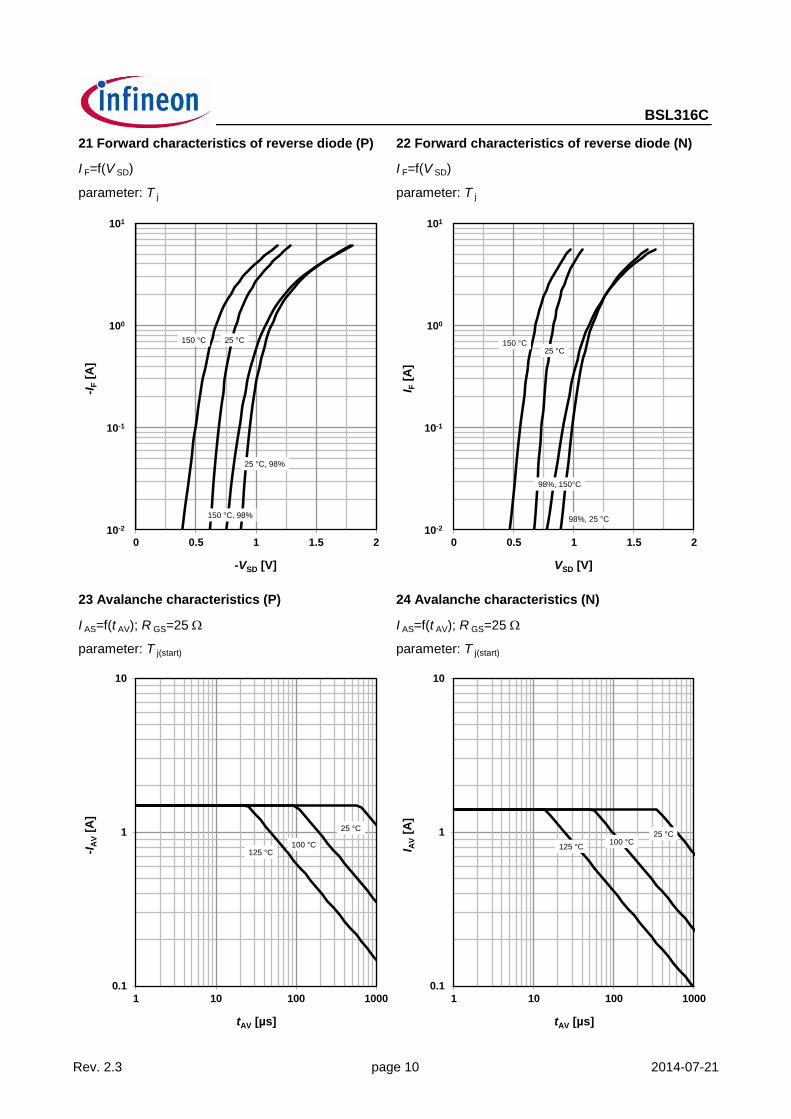
21 Forward characteristics of reverse diode (P) 22 Forward characteristics of reverse diode (N)
I F=f(V SD) I F=f(V SD)
parameter: T j parameter: T j
23 Avalanche characteristics (P) 24 Avalanche characteristics (N)
I AS=f(t AV); R GS=25 W I AS=f(t AV); R GS=25 W
parameter: T j(start) parameter: T j(start)
25 °C
100 °C 125 °C
0.1
1
10
1 10 100 1000
-IA
V [
A]
tAV [µs]
25 °C 100 °C
125 °C
0.1
1
10
1 10 100 1000
I AV [
A]
tAV [µs]
25 °C 150 °C
25 °C, 98%
150 °C, 98%
10-2
10-1
100
101
0 0.5 1 1.5 2
-IF [
A]
-VSD [V]
25 °C 150 °C
98%, 25 °C
98%, 150°C
10-2
10-1
100
101
0 0.5 1 1.5 2
I F [
A]
VSD [V]
Rev. 2.3 page 10 2014-07-21
BSL316C
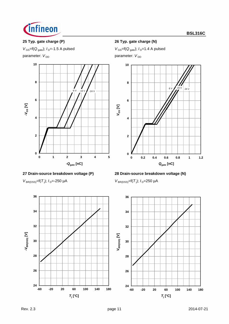
25 Typ. gate charge (P) 26 Typ. gate charge (N)
V GS=f(Q gate); I D=-1.5 A pulsed V GS=f(Q gate); I D=1.4 A pulsed
parameter: V DD parameter: V DD
27 Drain-source breakdown voltage (P) 28 Drain-source breakdown voltage (N)
V BR(DSS)=f(T j); I D=-250 µA V BR(DSS)=f(T j); I D=250 µA
24
26
28
30
32
34
36
-60 -20 20 60 100 140 180
-VB
R(D
SS
) [V
]
Tj [°C]
24
26
28
30
32
34
36
-60 -20 20 60 100 140 180
VB
R(D
SS
) [V
]
Tj [°C]
-6 V -15 V -24 V
0
2
4
6
8
10
0 1 2 3 4 5
-VG
S [
V]
-Qgate [nC]
6 V 15 V 24 V
0
2
4
6
8
10
0 0.2 0.4 0.6 0.8 1 1.2
VG
S [
V]
Qgate [nC]
Rev. 2.3 page 11 2014-07-21
BSL316C
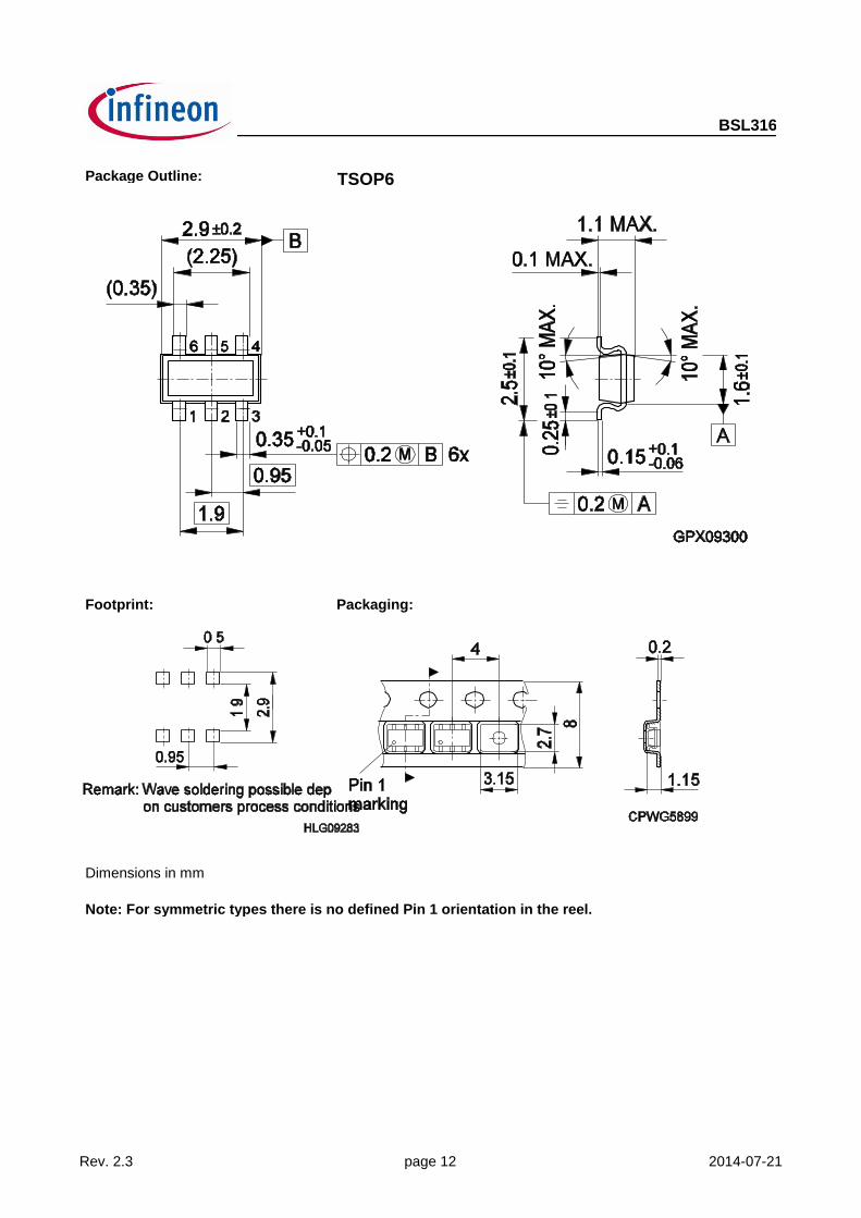
Package Outline:
Footprint: Packaging:
Dimensions in mm
Note: For symmetric types there is no defined Pin 1 orientation in the reel.
TSOP6
Rev. 2.3 page 12 2014-07-21
BSL316C
Published by
Infineon Technologies AG
81726 Munich, Germany
© 2008 Infineon Technologies AG
All Rights Reserved.
Legal Disclaimer
The information given in this document shall in no event be regarded as a guarantee of
conditions or characteristics. With respect to any examples or hints given herein, any typical
values stated herein and/or any information regarding the application of the device,
Infineon Technologies hereby disclaims any and all warranties and liabilities of any kind,
including without limitation, warranties of non-infringement of intellectual property rights
of any third party.
Information
For further information on technology, delivery terms and conditions and prices, please
contact the nearest Infineon Technologies Office (www.infineon.com).
Warnings
Due to technical requirements, components may contain dangerous substances. For information
on the types in question, please contact the nearest Infineon Technologies Office.
Infineon Technologies components may be used in life-support devices or systems only with
the express written approval of Infineon Technologies, if a failure of such components can
reasonably be expected to cause the failure of that life-support device or system or to affect
the safety or effectiveness of that device or system. Life support devices or systems are
intended to be implanted in the human body or to support and/or maintain and sustain
and/or protect human life. If they fail, it is reasonable to assume that the health of the user
or other persons may be endangered.
Rev. 2.3 page 13 2014-07-21


![ECEN325: Electronics Spring 2021[Sedra/Smith] L x V GC x V GS V x V GS V DS • When V DS V GS-V TH=V OV, V GC no longer exceeds V TH, resulting in the channel “pinching off” and](https://img.pdfslide.net/doc/110x75/612a01ce79234c2dda6a1604/ecen325-electronics-spring-2021-sedrasmith-l-x-v-gc-x-v-gs-v-x-v-gs-v-ds-a.jpg)