Embed Size (px)
Citation preview
Progress In Electromagnetics Research B, Vol. 32, 283–297, 2011
OPTIMUM HIGH IMPEDANCE SURFACE CONFIGU-RATION FOR MUTUAL COUPLING REDUCTION INSMALL ANTENNA ARRAYS
N. Capet 1, *, C. Martel 2, J. Sokoloff 3, and O. Pascal 3
1CNES, Antenna Department, 18 Avenue E. Belin, 31401 Toulousecedex 9, France2ONERA-DEMR, 2 Avenue E. Belin, BP 4025, Toulouse 31055, France3Universite de Toulouse UPS, INPT, CNRS LAPLACE (LaboratoirePlasma et Conversion d’Energie), 118 Route de Narbonne, F-31062Toulouse cedex 9, France
Abstract—In this paper, the electromagnetic properties of two differ-ent High Impedance Surfaces (HIS) with or without ElectromagneticBand Gap (EBG) in different configurations are investigated for mutualcoupling reduction in small antenna arrays. The resonant mechanismsof these structures are studied using transmission calculations in a par-allel plate waveguide. An optimum configuration is then proposed. Itis shown that a good isolation performance can be achieved withoutthe need of metallic vias when the structure is embedded in a metal-lic cavity, which limits significantly the number of HIS cells needed toperform a good isolation and the cost of manufacture.
1. INTRODUCTION
Mutual couplings in an array can represent severe drawbacks insome applications. In Controlled Reception Pattern Antenna (CRPA)applications, the antenna generally consists of an array of a fewelements separated by a physical distance of about half a free spacewavelength [1]. Therefore, mutual couplings between the elements ofthe array are generally strong and degrade the antenna and overallsystem performances [2]. Numerous strategies can be used to reducemutual coupling in an array such as: corrugations [3, 4], Split Ring
Received 5 May 2011, Accepted 9 July 2011, Scheduled 20 July 2011* Corresponding author: Nicolas Capet ([email protected]).
284 Capet et al.
Resonators (SRR) [5] and Defected Ground Structures (DGS) [6, 7].Moreover, mushroom like High Impedance Surfaces (HIS) are welldescribed in [8] and are well known to suppress surface waves and thusto improve the isolation of radiating elements in an array. This articlefocuses on such HIS technology and the way to optimize the insertionof the structure in a small array. Although the metamaterial unit cellsof the HIS are very small compared to the wavelength, typically belowλ0/10, only a few rows of these structures can be inserted betweenthe elements. Thus a trade-off between mutual coupling and the inter-element distance reduction has to be made.
Many different Electronic Band Structures based on mushroomlike HIS as introduced in [8] have been designed and inserted betweentwo antennas to reduce the coupling levels [9–13]. Generally, thesestructures consist of metallic patches printed on the substrate of thepatch antennas and connected or not to the ground plane with ametallic vias. For single layer structures, the size of the patches isabout half the substrate wavelength [11]. We can easily understandthat this type of structure can not be used for CRPA applications dueto the size of the unit cell. Thus, to optimize the compactness, a simpledesign of a two layered High Impedance Surface structure will be usedinspired from [14], although further improvements in terms of size andcost can be achieved [15].
The use of metallic vias has been studied in our previousworks [16, 17]. Their removal presents some advantages. Indeed,their manufacture is restrictive, especially regarding to the maximumthickness allowed by standard industrial processes. They are soexpensive to build that their cost can represent a significant part ofthe total price of the antenna. Moreover, their radii can also lead tointeresting discussions as the so called plasmonic resonance is relatedto this parameter [18, 19]. However, this topic is not developed inthe present paper since our goal is to improve the isolation betweenradiating elements using a structure without vias.
In this paper, two high impedance surfaces are studied: one withmetallic vias, the other without. Their capability to suppress surfacewaves has already been modeled and discussed in [20]. In the presentpaper, a conventional study of an infinite lattice of HIS cells is carriedout leading to useful field distribution on an elementary cell. Theresonant mechanisms of these structures with a limited number of cellsare then studied in view of being integrated within an array. The waythe structure is inserted is also assessed and highlights the impact ofedge effects.
In Section 2, the designs of two square shaped HIS with or withoutmetallic vias are presented together with their high impedance surface
Progress In Electromagnetics Research B, Vol. 32, 2011 285
properties. The dispersion properties of these structures highlight theirdifferences.
In Section 3, an innovative means of characterizing the computedperformances of the HIS for mutual coupling reduction is used(Figure 6) to study its frequency behavior. It is shown that thecapability of the HIS with EBG is greatly affected by its size (i.e.,the number of cells of the HIS has an impact on both the frequencystop bands and the attenuation levels) (Figures 7 and 8). Two differentconfigurations are studied: when the HIS with EBG is embedded ornot.
Finally, a study of the resonant processes is carried out inSection 4 for both structures (with and without vias) and bothconfigurations (embedded or non embedded). It is shown that theuse of the embedded configuration enables the excitation of the HISresonance independently of the number of cells. As a consequence,this configuration enables an efficient mutual coupling reduction witha very limited number of cells. Moreover, it allows the suppression ofthe metallic vias — i.e., the use of HIS with no EBG — while keepinggood isolation properties.
2. HIGH IMPEDANCE SURFACES
2.1. Design of Two Layered HIS
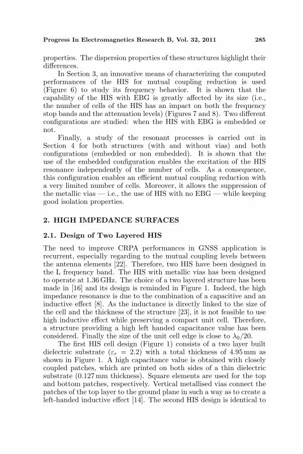
The need to improve CRPA performances in GNSS application isrecurrent, especially regarding to the mutual coupling levels betweenthe antenna elements [22]. Therefore, two HIS have been designed inthe L frequency band. The HIS with metallic vias has been designedto operate at 1.36GHz. The choice of a two layered structure has beenmade in [16] and its design is reminded in Figure 1. Indeed, the highimpedance resonance is due to the combination of a capacitive and aninductive effect [8]. As the inductance is directly linked to the size ofthe cell and the thickness of the structure [23], it is not feasible to usehigh inductive effect while preserving a compact unit cell. Therefore,a structure providing a high left handed capacitance value has beenconsidered. Finally the size of the unit cell edge is close to λ0/20.
The first HIS cell design (Figure 1) consists of a two layer builtdielectric substrate (εr = 2.2) with a total thickness of 4.95mm asshown in Figure 1. A high capacitance value is obtained with closelycoupled patches, which are printed on both sides of a thin dielectricsubstrate (0.127 mm thickness). Square elements are used for the topand bottom patches, respectively. Vertical metallised vias connect thepatches of the top layer to the ground plane in such a way as to create aleft-handed inductive effect [14]. The second HIS design is identical to
286 Capet et al.
Figure 1. View in 3 dimensions of the HIS cell with metallic vias(a1 = 10 mm, a2 = 5.35mm, acell = 14mm, h = 4.95mm).
the first one except that no vertical metallised vias connect the patchesof the top layer to the ground plane. Square shaped patches have beenchosen for convenience in the observation of the studied fields.
2.2. High Impedance Effect
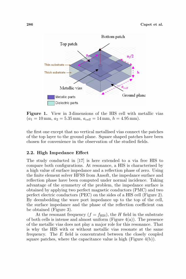
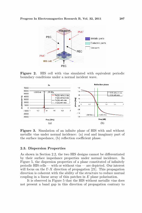
The study conducted in [17] is here extended to a via free HIS tocompare both configurations. At resonance, a HIS is characterised bya high value of surface impedance and a reflection phase of zero. Usingthe finite element solver HFSS from Ansoft, the impedance surface andreflection phase have been computed under normal incidence. Takingadvantage of the symmetry of the problem, the impedance surface isobtained by applying two perfect magnetic conductors (PMC) and twoperfect electric conductors (PEC) on the sides of a HIS cell (Figure 2).By deembedding the wave port impedance up to the top of the cell,the surface impedance and the phase of the reflection coefficient canbe obtained (Figure 3).
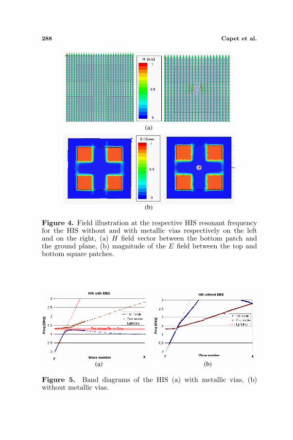
At the resonant frequency (f = fHIS), the H field in the substrateof both cells is intense and almost uniform (Figure 4(a)). The presenceof the metallic vias does not play a major role for this resonance. Thatis why the HIS with or without metallic vias resonate at the samefrequency. The E field is concentrated between the closely coupledsquare patches, where the capacitance value is high (Figure 4(b)).
Progress In Electromagnetics Research B, Vol. 32, 2011 287
Figure 2. HIS cell with vias simulated with equivalent periodicboundary conditions under a normal incident wave.
(a) (b)
Figure 3. Simulation of an infinite plane of HIS with and withoutmetallic vias under normal incidence: (a) real and imaginary part ofthe surface impedance, (b) reflection coefficient phase.
2.3. Dispersion Properties
As shown in Section 2.2, the two HIS designs cannot be differentiatedby their surface impedance properties under normal incidence. InFigure 5, the dispersion properties of a plane constituted of infinitelyperiodic HIS cells — with or without vias — are depicted. Our interestwill focus on the Γ-X direction of propagation [21]. This propagationdirection is coherent with the ability of the structure to reduce mutualcoupling in a linear array of thin patches in E plane polarisation.
It is observed in Figure 5 that the HIS without metallic vias doesnot present a band gap in this direction of propagation contrary to
288 Capet et al.
(a)
(b)
Figure 4. Field illustration at the respective HIS resonant frequencyfor the HIS without and with metallic vias respectively on the leftand on the right, (a) H field vector between the bottom patch andthe ground plane, (b) magnitude of the E field between the top andbottom square patches.
(a) (b)
Figure 5. Band diagrams of the HIS (a) with metallic vias, (b)without metallic vias.
Progress In Electromagnetics Research B, Vol. 32, 2011 289
the HIS with metallic vias. Thus, the HIS without vias might not beable to stop surface currents propagation and reduce mutual couplingbetween antennas. It is consistent with [14, 20] and [23] and confirmsthat the first mode is disturbed by the presence of the vias, whichinduces the band gap — the inductive effect works as a low pass forthe first mode. Thus, the computation of the band diagrams highlightsthe differences between the two structures.
3. PROPERTIES OF A FINITE HIS
3.1. Description of the Setup
In Section 2, we have computed some electromagnetic properties ofan infinite plane constituted of periodic HIS cells. Since the space islimited between the radiating elements of the array, the EM propertiesof a few periods of both HIS structure is considered.
It has been shown that the HIS resonant frequency of suchmushroom structures is slightly shifted depending on the angle of theincident wave [11]. Within a linear array of thin patches in E planepolarisation, it can be assumed that the coupling between the elementsis in the form of grazing incidence. In view of characterising theproperties of the HIS in these conditions, transmission measurementsof a waveguide containing the two types of HIS are carried out. Thefollowing setup is valid as far as the coupling between the radiatingelements is mainly due to TM0 substrate modes, which is the case forthin patches or cavity backed patch antennas [24].
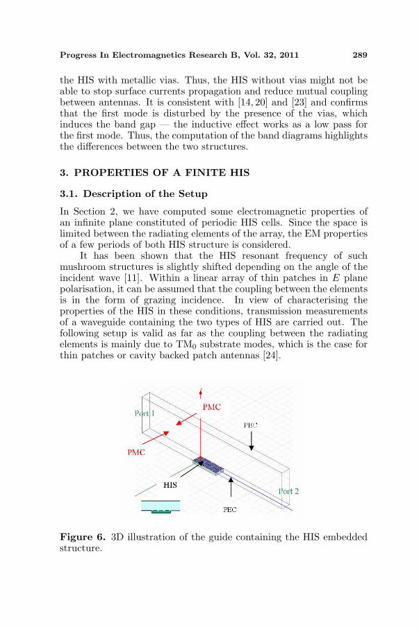
Figure 6. 3D illustration of the guide containing the HIS embeddedstructure.
290 Capet et al.
The wave guide is composed of two perfect metallic plates onthe top and the bottom. The HIS is inserted in the wave guide intwo different ways: on or embedded in a metallic cavity connectedto the bottom plate of the guide (as illustrated in Figure 6) — theembedded configuration is studied as it has the potential to isolateradiating elements more efficiently [16, 17]. The number of cells of theHIS can be adjusted. When the cells are not embedded, the groundof the cells corresponds to the bottom metallic part of the guide. Thewalls of the guide are composed of perfect magnetic conductors. Thus,a TEM mode can propagate in this guide.
This means of characterisation is relevant of the couplingphenomenon between two patch antennas. Indeed, for wavespropagating from one microstrip antenna to another, the E field vectoris predominantly normal to the ground plane surface and the H field ismainly contained in the plane orthogonal to the propagation directionand tangential to the ground plane.
3.2. Transmission Results
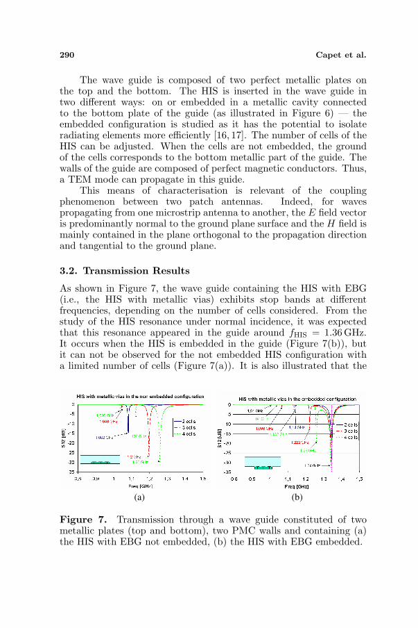
As shown in Figure 7, the wave guide containing the HIS with EBG(i.e., the HIS with metallic vias) exhibits stop bands at differentfrequencies, depending on the number of cells considered. From thestudy of the HIS resonance under normal incidence, it was expectedthat this resonance appeared in the guide around fHIS = 1.36 GHz.It occurs when the HIS is embedded in the guide (Figure 7(b)), butit can not be observed for the not embedded HIS configuration witha limited number of cells (Figure 7(a)). It is also illustrated that the
(a) (b)
Figure 7. Transmission through a wave guide constituted of twometallic plates (top and bottom), two PMC walls and containing (a)the HIS with EBG not embedded, (b) the HIS with EBG embedded.
Progress In Electromagnetics Research B, Vol. 32, 2011 291
(a) (b)
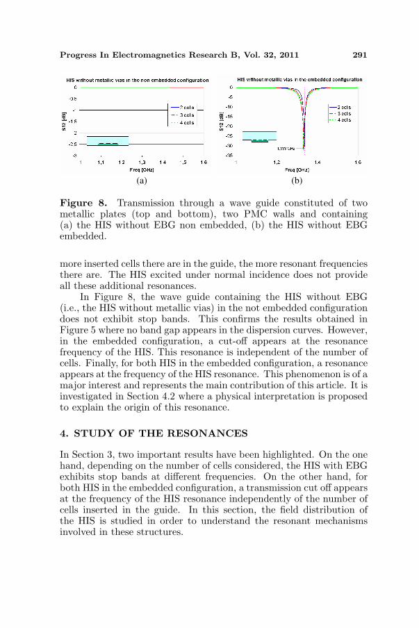
Figure 8. Transmission through a wave guide constituted of twometallic plates (top and bottom), two PMC walls and containing(a) the HIS without EBG non embedded, (b) the HIS without EBGembedded.
more inserted cells there are in the guide, the more resonant frequenciesthere are. The HIS excited under normal incidence does not provideall these additional resonances.
In Figure 8, the wave guide containing the HIS without EBG(i.e., the HIS without metallic vias) in the not embedded configurationdoes not exhibit stop bands. This confirms the results obtained inFigure 5 where no band gap appears in the dispersion curves. However,in the embedded configuration, a cut-off appears at the resonancefrequency of the HIS. This resonance is independent of the number ofcells. Finally, for both HIS in the embedded configuration, a resonanceappears at the frequency of the HIS resonance. This phenomenon is of amajor interest and represents the main contribution of this article. It isinvestigated in Section 4.2 where a physical interpretation is proposedto explain the origin of this resonance.
4. STUDY OF THE RESONANCES
In Section 3, two important results have been highlighted. On the onehand, depending on the number of cells considered, the HIS with EBGexhibits stop bands at different frequencies. On the other hand, forboth HIS in the embedded configuration, a transmission cut off appearsat the frequency of the HIS resonance independently of the number ofcells inserted in the guide. In this section, the field distribution ofthe HIS is studied in order to understand the resonant mechanismsinvolved in these structures.
292 Capet et al.
4.1. The Non HIS Resonances (f 6= fHIS)
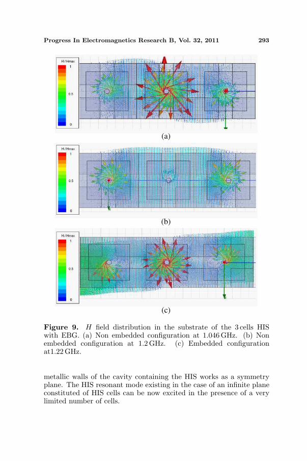
The wave guide containing the HIS with EBG (i.e., the HIS withmetallic vias) exhibits stop bands at different frequencies, dependingon the number of cells considered. In Figure 9, the H field distributionat some of non HIS resonant frequencies for the 3 cells HIS with EBGis depicted.
As expected from its frequency response, for resonant frequenciesdifferent from the HIS resonant frequency (f 6= fHIS), the nonembedded configuration does not exhibit the H field distribution at theHIS resonance in the presence of a limited number of cells (Figures 9(a)and 9(b)). Its shows that the environmental conditions of the HIS donot allow this resonance obtained in the case of an infinite plane.
In addition, it can be seen from Figure 9 that the H fieldorientation is not the same in the three cells. It illustrates that aresonance can be generated by a group of cells and affected by thepresence of the metallic cavity. It is the case for all resonances,except the HIS resonance discussed in the Section 4.2. This is furtherillustrated in Figure 7, where various resonances can be observeddepending on the configuration and the number of cells considered.It also explains the increase in the number of resonances as more cellsare introduced in the guide.
4.2. The HIS Resonances (f = fHIS)
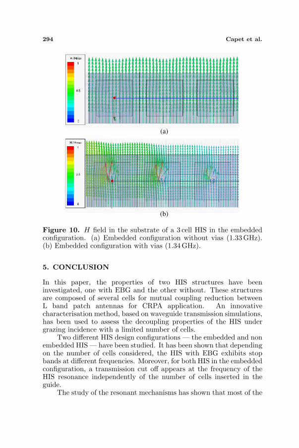
In this section, the field distributions of the 3 HIS cells structuresembedded in the wave guide are studied at the HIS resonance.
In Figure 10, the H field in the substrate of a 3 cell HIS withor without EBG embedded is shown at the HIS resonance. We cannotice that the H field distribution is uniform in the substrate of theHIS without EBG and all these three cells resonate in phase with thesame H field orientation. In the case of the HIS with EBG, we cannotice that the H field distributions of the cells are similar. However,a uniform attenuation can be observed from cell to cell in the directionof wave propagation. For both cases each cell then works as when itwas infinitely periodised and normally illuminated (Figure 4) and thesame transmission levels are observed at this frequency (Figures 7(b)and 8(b)). This explains why Figure 4(a) is almost in accordancewith Figure 10. It can be observed that the same high impedanceresonance and frequency are achieved whether the two HIS are excitedunder normal or grazing incidence, independently of the number ofcells considered. The edge effects introduced by the cavity containingthe HIS recreate the necessary conditions for the apparition of the HISresonance. Indeed, due to the shape of the HIS resonant mode, the
Progress In Electromagnetics Research B, Vol. 32, 2011 293
(a)
(b)
(c)
Figure 9. H field distribution in the substrate of the 3 cells HISwith EBG. (a) Non embedded configuration at 1.046 GHz. (b) Nonembedded configuration at 1.2GHz. (c) Embedded configurationat1.22GHz.
metallic walls of the cavity containing the HIS works as a symmetryplane. The HIS resonant mode existing in the case of an infinite planeconstituted of HIS cells can be now excited in the presence of a verylimited number of cells.
294 Capet et al.
(a)
(b)
Figure 10. H field in the substrate of a 3 cell HIS in the embeddedconfiguration. (a) Embedded configuration without vias (1.33 GHz).(b) Embedded configuration with vias (1.34GHz).
5. CONCLUSION
In this paper, the properties of two HIS structures have beeninvestigated, one with EBG and the other without. These structuresare composed of several cells for mutual coupling reduction betweenL band patch antennas for CRPA application. An innovativecharacterisation method, based on waveguide transmission simulations,has been used to assess the decoupling properties of the HIS undergrazing incidence with a limited number of cells.
Two different HIS design configurations — the embedded and nonembedded HIS — have been studied. It has been shown that dependingon the number of cells considered, the HIS with EBG exhibits stopbands at different frequencies. Moreover, for both HIS in the embeddedconfiguration, a transmission cut off appears at the frequency of theHIS resonance independently of the number of cells inserted in theguide.
The study of the resonant mechanisms has shown that most of the
Progress In Electromagnetics Research B, Vol. 32, 2011 295
resonances are based on multiple cells. This explains the frequencydependence regarding the number of cells considered. However, inthe embedded configuration, the side effects introduced by the cavitycontaining the HIS recreate the necessary conditions for the apparitionof the HIS resonance. This explains why this resonance appearsindependently of the number of the cells.
In conclusion, it has been shown that the HIS structure in theembedded configuration provides the optimum performance for ourapplication. It allows the use of a very limited number of cells whilepreserving a good isolation. It can also be noticed that the HIS withmetallic vias allows multi-frequency isolation. Moreover, the designdoes not require metallic vias, which limits significantly the cost ofmanufacture.
As shown in this paper with a basic HIS cell and considering thediversity of possible HIS topologies, similar studies could be done withother kind of unit cells. Complementary experimental works will beperformed to confirm the promising simulation results of this paper.
ACKNOWLEDGMENT
N. Capet wishes to acknowledge ONERA (The French Aerospace Lab)for providing the funding and the place for this work during his Ph.Doctor courses.
REFERENCES
1. Van Trees, H. L., Optimum Array Processing, Part IVof Detection, Estimation, and Modulation Theory, Wiley-Interscience, 2002.
2. Ngai, E. C. and D. J. Blejer, “Mutual coupling analyses for smallGPS adaptive arrays,” IEEE Antennas and Propagation SocietyInternational Symposium, Vol. 4, 3841, 2001.
3. Kildal, P.-S., “Artificially soft and hard surfaces in electromag-netics and their application to antenna design,” 23rd EuropeanMicrowave Conference, 30–33, Sep. 6–10, 1993.
4. Rajo-Iglesias, E., O. Quevedo-Teruel, and L. Inclan-Sanchez,“Planar soft surfaces and their application to mutual couplingreduction,” IEEE Transactions on Antennas and Propagation,Vol. 57, No. 12, 3852–3859, Dec. 2009.
5. Buell, K., H. Mosallaei, and K. Sarabandi, “Electromagneticmetamaterial insulator to eliminate substrate surface waves,”
296 Capet et al.
IEEE Antennas and Propagation Society International Sympo-sium, Vol. 2A, 574–577, Jul. 3–8, 2005.
6. Guha, D., S. Biswas, M. Biswas, J. Y. Siddiqui, andY. M. M. Antar, “Concentric ring-shaped defected groundstructures for microstrip applications,” IEEE Antennas andWireless Propagation Letters, Vol. 5, No. 1, 402–405, Dec. 2006.
7. Chiu, C.-Y., C.-H. Cheng, R. D. Murch, and C. R. Rowell,“Reduction of mutual coupling between closely-packed antennaelements,” IEEE Transactions on Antennas and Propagation,Vol. 55, No. 6, 1732–1738, Jun. 2007.
8. Sievenpiper, D., L. Zhang, R. F. J. Broas, N. G. Alexopolous, andE. Yablonovitch, “High impedance electromagnetic surfaces witha forbidden frequency band,” IEEE Transactions on MicrowaveTheory and Techniques, Vol. 47, No. 11, Nov. 1999.
9. Yang, F. and Y. Rahmat-Samii, “Microstrip antennas integratedwith electromagnetic band-gap (EBG) structures: A low mutualcoupling design for array applications,” IEEE Transactions onAntennas and Propagation, Vol. 51, No. 10, 2936–2946, Oct. 2003.
10. Simovski, C. R. and A. A. Sochava, “High-impedance surfacesbased on self-resonant grids. Analytical modelling and numericalsimulations,” Progress In Electromagnetics Research, Vol. 43, 239–256, 2003.
11. E. Rajo-Iglesias, O. Quevedo-Teruel, and L. Inclan-Sanchez,“Mutual coupling reduction in patch antenna arrays by using aplanar EBG structure and a multilayer dielectric substrate,” IEEETransactions on Antennas and Propagation, Vol. 56, No. 6, 1648–1655, Jun. 2008.
12. Fan, M. Y., R. Hu, Z. H. Feng, X. X. Zhang, and Q. Hao,“Advance in 2D-EBG research,” Journal of Infrared MillimeterWaves, Vol. 22, No. 2, 2003.
13. Lin, B.-Q., Q.-R. Zheng, and N.-C. Yuan, “A novel spiral highimpedance surface structure for size reduction,” Microwave andOptical Technology Letters, Vol. 49, No. 9, Sep. 2007.
14. Caloz, C. and T. Itoh, Electromagnetic Metamaterials: Transmis-sion Line Theory and Microwave Applications: The EngineeringApproach, Wiley-Interscience, 2006.
15. Costa, F., S. Genovesi, and A. Monorchio, “On the bandwidthof high-impedance frequency selective surfaces,” IEEE Antennasand Wireless Propagation Letters, Vol. 8, 1341–1344, 2009.
16. Capet, N., C. Martel, J. Sokoloff, and O. Pascal, “Reduction ofthe mutual coupling between two adjacent patches using various
Progress In Electromagnetics Research B, Vol. 32, 2011 297
ideal High Impedance Surface positionings,” Proceedings of the3rd European Conference on Antennas and Propagation, EuCAP2009, 3151–3154, Mar. 23–27, 2009.
17. Capet, N., C. Martel, J. Sokoloff, and O. Pascal, “Study ofthe behaviour of a two layered high impedance surface withelectromagnetic band gap,” Proceedings of the Fourth EuropeanConference on Antennas and Propagation, EuCAP 2010, 1–4,Apr. 12–16, 2010.
18. Luukkonen, O., M. G. Silveirinha, A. B. Yakovlev, C. R. Simovski,I. S. Nefedov, and S. A. Tretyakov, “Effects of spatial dispersionon reflection from mushroom-type artificial impedance surfaces,”IEEE Transactions on Microwave Theory and Techniques, Vol. 57,No. 11, 2692–2699, Nov. 2009.
19. Luukkonen, O., F. Costa, C. R. Simovski, A. Monorchio, andS. A. Tretyakov, “A thin electromagnetic absorber for wideincidence angles and both polarizations,” IEEE Transactions onAntennas and Propagation, Vol. 57, No. 10, 3119–3125, Oct. 2009.
20. Luukkonen, O., A. B. Yakovlev, C. R. Simovski, andS. A. Tretyakov, “Comparative study of surface waves on high-impedance surfaces with and without vias,” IEEE Antennas andPropagation Society International Symposium, 1–4, Jul. 5–11,2008.
21. Joannopoulos, J. D., S. G. Johnson, J. N. Winn, and R. D. Meade,Photonic Crystals: Molding the Flow of Light, 2nd edition,Princeton University Press, 2008.
22. Ngai, E. C. and D. J. Blejer, “Mutual coupling analyses for smallGPS adaptive arrays,” MIT Lincoln Laboratory, 2001.
23. Rahmat-Samii, Y., “EBG structures for low profile antennadesigns: What have we learned?,” Proceedings of the SecondEuropean Conference on Antennas and Propagation, EuCAP2007, 1–5, Nov. 11–16, 2007.
24. Pozar, D., “Considerations for millimeter wave printed antennas,”IEEE Transactions on Antennas and Propagation, Vol. 31, No. 5,740–747, Sep. 1983.