Embed Size (px)
Citation preview
Materials Letters 66 (2012) 270–272
Contents lists available at SciVerse ScienceDirect
Materials Letters
j ourna l homepage: www.e lsev ie r .com/ locate /mat le t
Optoelectronic characteristics of single ZnAlO nanotetrapod
Feifei Wang a, Chong Wang b,⁎, Jiannong Chen a, Yongjiang Yu a
a School of Physics, Ludong University, Yantai 264025, Chinab Institute of Optic Electro Information, Yantai University, 264005, China
⁎ Corresponding author. Tel.: +86 535 690 1947; faxE-mail address: [email protected] (C. Wang).
0167-577X/$ – see front matter © 2011 Elsevier B.V. Aldoi:10.1016/j.matlet.2011.08.070
a b s t r a c t
a r t i c l e i n f oArticle history:Received 21 June 2011Accepted 19 August 2011Available online 26 August 2011
Keywords:Nanocrystalline materialsElectrical properties
The ZnAlO nanotetrapods were prepared by a simple thermal evaporation method. The typical characteristicsof I–V curves for one of our devices illustrated that both the green light and the UV light could induce the in-creasing of conductance, but the conductance under the UV light is much larger than that under the illumi-nation of green light. With the increasing of temperature, the conductance of the sample is also increased.Furthermore, the change of current versus time as the UV light is switched on and off shows the samplehas good switch characteristics. These findings illustrate the sample may be used in room temperaturelight sensors.
: +86 535 690 1947.
l rights reserved.
© 2011 Elsevier B.V. All rights reserved.
1. Introduction
Nowadays, nanomaterials have attracted great attention due totheir promising applications in nanodevices. Photodetector is alsoone of the most important applications of semiconductor materials.So far, the photoconducting properties of semiconductor materialssuch as ZnO[1], SnO2[2], GaN[3], and CdS[4] have been investigated.Yet, the report on photoconducting properties of metal elementdoped or alloyed ZnO nanostructures is few [5,6]. In recent years,great efforts have been taken to investigate ZnO nanostructureswith various metal element doped or alloyed, such as Mg, Sn and In[7–9], due to their potential applications in optoelectronic devices.Among them, ZnAlO nanomaterials, with high crystal quality, goodfield emission and ultraviolet detector property, have also beenreported [10–13]. However, the photoconducting properties ofthree-dimensional branched nanostructured ZnAlO have not beenreported yet.
In this paper, we reported the preparation of ZnAlO nanotetrapodsby a simple thermal evaporation method. The current–voltage (I–V)curves of the sample were obtained at the illumination of green andUV light. The electric properties at different temperature were alsostudied. Furthermore, the change of photocurrent versus time was in-vestigated as the UV light is switched on and off. Compared with thephotoconductivity reported in literature 13, the single ZnAlO nanote-trapod has shorter recovery time to UV light, which suggested that itis a good candidate for optoelectronic switches.
2. Experimental procedure
ZnAlO nanotetrapods were synthesized through a simple thermalevaporation method. The Al and Zn mixed powders with the weightratio of 1:5 were loaded in an alumina boat and Si substrates withthin (4 nm) Au film sputtered were positioned on the boat. The boatwas then placed at the center of a quartz tube which was insertedinto a horizontal tube furnace. The furnace was heated to 960 °Cwith a mix gas of argon and oxygen at the flow rate of 100 sccmand kept at this temperature for 1 h. After the furnace was cooleddown to room temperature naturally, the substrates covered withthe resulting products were collected.
The morphology of the as-synthesized sample was characterized byscanning electron microscopy (SEM, Hitachi, S-4200) and the chemicalcomposition analysis was achieved by energy-dispersive X-ray spec-troscopy (EDS) attached to SEM. The crystal structure was analyzedby X-ray diffraction (XRD, Japan, Rigaku, D/MAX-2400) with graphite-monochromatized Cu Kα radiation (λ=1.54178 Å). A CW He–Cdlaser (50 mW, wavelength at 325 nm, IK 3552R-G) was used to mea-sure the photoluminescence (PL) of the sample. The device used forphotoconducting characteristics was fabricated by conventional photo-lithography. The electrodes of Au with a thickness of 50 nm were de-posited by e-beam deposition on a silicon substrate with a 500 nmthick thermally grown SiO2 layer. Then individual nanotetrapods areplaced on the top of the electrodes. The separation between the twoelectrodes is about 1.2 μm. All the measures were taken in air.
3. Results and discussion
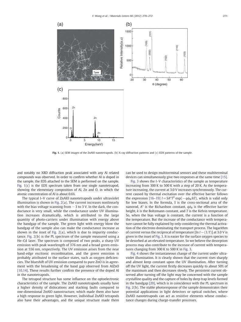
Fig. 1(a) is the SEM image of the as-prepared sample, it is indicatedthat each individual structure is consisted of tetrahedrally arranged rod-like legs. Fig. 1(b) is XRD profile pattern of the nanomaterials, almost allsharp peaks coincide with the peaks of zincite ZnO (JCPDS: 36-1451)
20 30 40 50 60
0
500
1000
1500
(b)
Rel
ativ
e In
tens
ity(a
.u)
(100
)(0
02)
(101
)
(102
)
(110
)
(103
)
(a)
(c)
800
600
400
200 O
Zn
Zn
Zn
00 5 10
Energy(keV)
Cou
nts
15
Fig. 1. (a) SEM images of the ZnAlO nanotetrapods. (b) X-ray diffraction patterns and (c) EDX patterns of the sample.
271F. Wang et al. / Materials Letters 66 (2012) 270–272
and notably no XRD diffraction peak associated with any Al relatedcompounds was observed. In order to confirm whether Al is doped inthe sample, the EDS attached to the SEM is performed on the sample.Fig. 1(c) is the EDS spectrum taken from one single nanotetrapod,showing the elementary composition of Al, Zn and O, in which theatomic concentration of Al is about 0.6%.
The typical I–V curve of ZnAlO nanotetrapods under ultravioletillumination is shown in Fig. 2(a). The current increases nonlinearlywith the bias voltage scanning from −3 to 3 V. In the dark, the con-ductance is very small, while the conductance under UV illumina-tion increases dramatically, which is attributed to the largequantity of photo-carriers under illumination with energy abovethe bandgap of the sample. The green light with energy blow thebandgap of the sample also can make the conductance increase asshown in the inset of Fig. 2(a), which is due to impurity conduc-tance. Fig. 2(b) is the PL spectrum of the sample measured using aHe–Cd laser. The spectrum is composed of two peaks, a sharp UVemission with peak wavelength of 376 nm and a broad green emis-sion at 556 nm, respectively. The UV emission arises from the nearband-edge excitonic recombination, and the green emission isprobably attributed to the surface states, such as oxygen deficien-cies. The blueshift of UV emission compared to pure ZnO is in agree-ment with the broadening of the band gap observed from AlZnO[10,14]. These results further confirm the presence of the doped Alin the nanotetrapods.
The tetrapod structure has some influence on the optoelectroniccharacteristics of the sample. The ZnAlO nanotetrapods usually havea higher density of dislocations and stacking faults compared toone-dimensional ZnAlO nanostructure, which made them also havea high response to green light. However, individual ZnAlO tetrapodsalso have their advantages, and the unique structure made them
can be used to design multiterminal sensors and these multiterminaldevices can simultaneously give two responses at the same time [15].
Fig. 3 shows the I–V characteristics of the sample as temperatureincreasing from 300 K to 500 K with a step of 20 K. As the tempera-ture increasing, the current at 3.0 V increases synchronously. The cur-rent caused by thermal excitation over the effective barrier followsthe expression [16–19] I=SA*T2 exp(−qϕB/kT), which is valid onlyfor low biases. In the formula, S is the cross-sectional area of thenanorod, A* is the Richardson constant, qϕB is the effective barrierheight, k is the Boltzmann constant, and T is the Kelvin temperature.So, when the bias voltage is constant, the current is a function ofthe temperature. But the increase of the conductance with tempera-ture cannot be fully explained by only considering the thermal activa-tion of the electrons dominating the transport process. The logarithmof current versus the reciprocal of temperature [ln I−(1/T)] at 3.0 V isgiven in the inset of Fig. 3. It is easier for the surface oxygen species tobe desorbed at an elevated temperature. So we believe the desorptionprocess may also contribute to the increase of current with tempera-tures changing from 300 K to 500 K in Fig. 3.
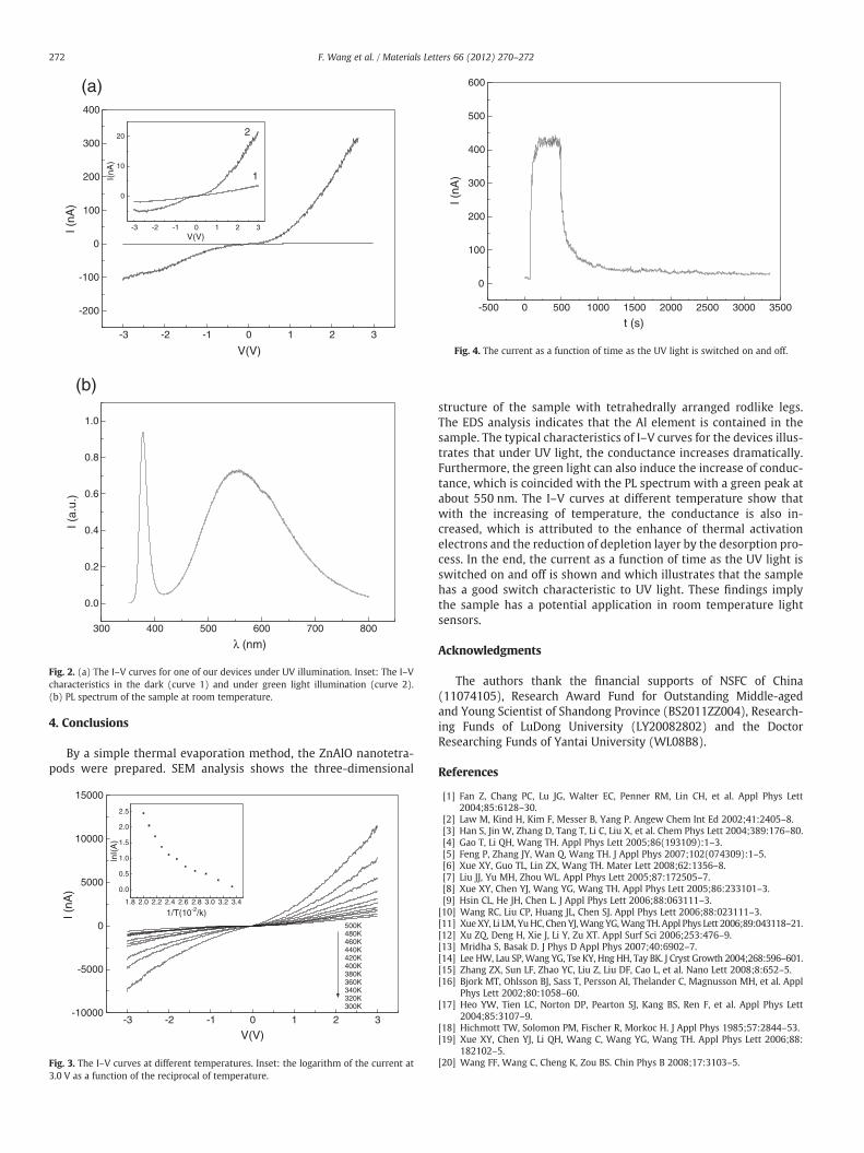
Fig. 4 shows the instantaneous change of the current under ultra-violet illumination. It is clearly shown that the current rises sharplyand almost keep constant upon the UV illumination. After turningoff the UV light, the current firstly decreases quickly to about 50% ofthe maximum and then decreases slowly. The persistent current ob-served after turning off the light may be concerned with the samplecrystalline quality and the capture of holes by deep trap levels formedin the bandgap [20], which is in coincidence with the PL spectrum inFig. 2(b). The stable photoresponse of the sample demonstrates theirpotential applications in light detectors or optical switches, whereZnAlO nanotetrapods can act as resistive elements whose conduc-tance changes during charge-transfer processes.
-200
-3 -2 -1 0 1 2 3
-3 -2 -1 0 1 2 3
-100
0
100
200
300
400
0
10
20
I(nA
)
V(V)
(a)
2
1
I (nA
)
V(V)
0.0
300 400 500 600 700 800
0.2
0.4
0.6
0.8
1.0
(b)
I (a.
u.)
λ (nm)
Fig. 2. (a) The I–V curves for one of our devices under UV illumination. Inset: The I–Vcharacteristics in the dark (curve 1) and under green light illumination (curve 2).(b) PL spectrum of the sample at room temperature.
0
100
200
300
400
500
-500 0 500 1000 1500 2000 2500 3000 3500
600
I (nA
)
t (s)
Fig. 4. The current as a function of time as the UV light is switched on and off.
272 F. Wang et al. / Materials Letters 66 (2012) 270–272
4. Conclusions
By a simple thermal evaporation method, the ZnAlO nanotetra-pods were prepared. SEM analysis shows the three-dimensional
-10000-3 -2 -1 0 1 2 3
-5000
0
5000
10000
15000
500K480K460K440K420K400K380K360K340K320K300K
0.0
1.8 2.0 2.2 2.4 2.6 2.8 3.0 3.2 3.4
0.5
1.0
1.5
2.0
2.5
lnI(
A)
1/T(10-2/k)I (nA
)
V(V)
Fig. 3. The I–V curves at different temperatures. Inset: the logarithm of the current at3.0 V as a function of the reciprocal of temperature.
structure of the sample with tetrahedrally arranged rodlike legs.The EDS analysis indicates that the Al element is contained in thesample. The typical characteristics of I–V curves for the devices illus-trates that under UV light, the conductance increases dramatically.Furthermore, the green light can also induce the increase of conduc-tance, which is coincided with the PL spectrum with a green peak atabout 550 nm. The I–V curves at different temperature show thatwith the increasing of temperature, the conductance is also in-creased, which is attributed to the enhance of thermal activationelectrons and the reduction of depletion layer by the desorption pro-cess. In the end, the current as a function of time as the UV light isswitched on and off is shown and which illustrates that the samplehas a good switch characteristic to UV light. These findings implythe sample has a potential application in room temperature lightsensors.
Acknowledgments
The authors thank the financial supports of NSFC of China(11074105), Research Award Fund for Outstanding Middle-agedand Young Scientist of Shandong Province (BS2011ZZ004), Research-ing Funds of LuDong University (LY20082802) and the DoctorResearching Funds of Yantai University (WL08B8).
References
[1] Fan Z, Chang PC, Lu JG, Walter EC, Penner RM, Lin CH, et al. Appl Phys Lett2004;85:6128–30.
[2] Law M, Kind H, Kim F, Messer B, Yang P. Angew Chem Int Ed 2002;41:2405–8.[3] Han S, Jin W, Zhang D, Tang T, Li C, Liu X, et al. Chem Phys Lett 2004;389:176–80.[4] Gao T, Li QH, Wang TH. Appl Phys Lett 2005;86(193109):1–3.[5] Feng P, Zhang JY, Wan Q, Wang TH. J Appl Phys 2007;102(074309):1–5.[6] Xue XY, Guo TL, Lin ZX, Wang TH. Mater Lett 2008;62:1356–8.[7] Liu JJ, Yu MH, Zhou WL. Appl Phys Lett 2005;87:172505–7.[8] Xue XY, Chen YJ, Wang YG, Wang TH. Appl Phys Lett 2005;86:233101–3.[9] Hsin CL, He JH, Chen L. J Appl Phys Lett 2006;88:063111–3.[10] Wang RC, Liu CP, Huang JL, Chen SJ. Appl Phys Lett 2006;88:023111–3.[11] XueXY, Li LM, YuHC, Chen YJ,Wang YG,Wang TH. Appl Phys Lett 2006;89:043118–21.[12] Xu ZQ, Deng H, Xie J, Li Y, Zu XT. Appl Surf Sci 2006;253:476–9.[13] Mridha S, Basak D. J Phys D Appl Phys 2007;40:6902–7.[14] Lee HW, Lau SP,Wang YG, Tse KY, Hng HH, Tay BK. J Cryst Growth 2004;268:596–601.[15] Zhang ZX, Sun LF, Zhao YC, Liu Z, Liu DF, Cao L, et al. Nano Lett 2008;8:652–5.[16] Bjork MT, Ohlsson BJ, Sass T, Persson AI, Thelander C, Magnusson MH, et al. Appl
Phys Lett 2002;80:1058–60.[17] Heo YW, Tien LC, Norton DP, Pearton SJ, Kang BS, Ren F, et al. Appl Phys Lett
2004;85:3107–9.[18] Hichmott TW, Solomon PM, Fischer R, Morkoc H. J Appl Phys 1985;57:2844–53.[19] Xue XY, Chen YJ, Li QH, Wang C, Wang YG, Wang TH. Appl Phys Lett 2006;88:
182102–5.[20] Wang FF, Wang C, Cheng K, Zou BS. Chin Phys B 2008;17:3103–5.