Embed Size (px)
Citation preview
Service Manual
Main Manual
© 2005 Panasonic Corporation of North America.
All rights reserved. Unauthorized copying
and distribution is a violation of law.
ORDER NO. MTNC050310C3
B01
Color Television
ChassisTMC573
This service manual is issued as a service guide for the model listed above.
Included in this manual are a set of schematic, block diagrams, functional descriptions, alignment procedures,
disassembly procedures and a complete parts list.
“WARNING! This Service Manual is designed for experienced repair technicians only and is not designed for use by the general public.
It does not contain warnings or cautions to advise non-technical individuals of potential dangers in attempting to service a product.
Products powered by electricity should be serviced or repaired only by experienced professional technicians. Any attempt to
service or repair the product or products dealt with in this Service Manual by anyone else could result in serious injury or death.”
The service technician is required to read and follow the “Safety Precautions” and “Important Safety Notice” in this Main Manual.
Panasonic
ModelsCT-Z1425
'CT-Z1425
'CT-Z1425
CONTENTS
A1-1
CONTENTS .................................................................................................................................................Important Safety Notice ............................................................................................................................Service Notes .............................................................................................................................................About lead free solder (PbF) ....................................................................................................................GENERAL SPECIFICATIONS ...................................................................................................................DISASSEMBLY INSTRUCTIONS
1. REMOVAL OF ANODE CAP ............................................................................................................2. NOTE FOR THE REMOVAL OF THE MAIN PCB ............................................................................
SERVICE MODE LIST ................................................................................................................................CONFIRMATION OF HOURS USED .........................................................................................................WHEN REPLACING EEPROM (MEMORY) IC ..........................................................................................ELECTRICAL ADJUSTMENTS
1. BEFORE MAKING ELECTRICAL ADJUSTMENTS .........................................................................2. BASIC ADJUSTMENTS ....................................................................................................................3. PURITY AND CONVERGENCE ADJUSTMENTS ...........................................................................4. ELECTRICAL ADJUSTMENT PARTS LOCATION GUIDE (WIRING CONNECTION) ...................
BLOCK DIAGRAM ......................................................................................................................................PRINTED CIRCUIT BOARDS
MAIN/CRT ..............................................................................................................................................SCHEMATIC DIAGRAMS
MICON/CHROMA/TUNER ..................................................................................................................... TV POWER ............................................................................................................................................
DEFLECTION/CRT ................................................................................................................................SOUND/AV .............................................................................................................................................
VOLTAGE LIST ..........................................................................................................................................WAVEFORMS .............................................................................................................................................MECHANICAL EXPLODED VIEW .............................................................................................................MECHANICAL REPLACEMENT PARTS LIST .........................................................................................ELECTRICAL REPLACEMENT PARTS LIST ...........................................................................................
A1-1A2-1A2-2, A2-3A2-4A3-1~A3-5
B-1B-1C-1C-1C-1
D-1D-1, D-2D-3D-4E-1, E-2
F-1~F-4
G-1, G-2G-3, G-4G-5, G-6G-7, G-8H-1I-1, I-2J-1K1-1K2-1~K2-3

A2-1
Important Safety Notice
Safety PrecautionsGeneral GuidelinesAn Isolation Transformer should always be usedduring the servicing of a receiver whose chassis is notisolated from AC power line. Use a transformer ofadequate power rating as this protects the technicianfrom accidents resulting in personal injury from electricalshocks. It will also protect the Receiver from beingdamaged by accidental shorting that may occur duringservicing.When servicing, observe the original lead dress,especially in the high voltage circuit. Replace alldamaged parts (also parts that show signs ofoverheating.)Always Replace Protective Devices, such asfishpaper, isolation resistors and capacitors, and shieldsafter servicing the Receiver. Use only manufacturer'srecommended rating for fuses, circuits breakers, etc.High potentials are present when this Receiver isoperating. Operation of the Receiver without the rearcover introduces danger for electrical shock. Servicingshould not be performed by anyone who is notthoroughly familiar with the necessary precautions whenservicing high-voltage equipment.Extreme care should be practiced when Handling thePicture Tube. Rough handling may cause it to implodedue to atmospheric pressure. (14.7 lbs per sq. in.). Donot nick or scratch the glass or subject it to any unduepressure. When handling, use safety goggles and heavygloves for protection. Discharge the picture tube byshorting the anode to chassis ground (not to the cabinetor to other mounting hardware). When dischargingconnect cold ground (i.e. dag ground lead) to the anodewith a well insulated wire or use a grounding probe.Avoid prolonged exposure at close range to unshieldedareas of the picture tube to prevent exposure to X-rayradiation.The Test Picture Tube used for servicing the chassis atthe bench should incorporate safety glass and magneticshielding. The safety glass provide shielding for the tubeviewing area against X-ray radiation as well asimplosion. The magnetic shield limits the X-ray radiationaround the bell of the picture tube in addition to therestricting magnetic effects. When using a picture tubetest jig for service, ensure that the jig is capable ofhandling 50kV without causing X-ray radiation.Before returning a serviced receiver to the owner,the service technician must thoroughly test the unit toensure that is completely safe to operate. Do not use aline isolation transformer when testing.Leakage Current Cold CheckUnplug the AC cord and connect a jumper between thetwo plug prongs.
Measure the resistance between the jumpered AC plugand expose metallic parts such as screwheads, antennaterminals, control shafts, etc. If the exposed metallicpart has a return path to the chassis, the reading shouldbe between 240k and 5.2M . If the exposed metallicpart does not have a return path to the chassis, thereading should be infinite.Leakage Current Hot Check (Fig. 1)
Plug the AC cord directly into the AC outlet. Do not usean isolation transformer during the check.Connect a 1.5k 10 watt resistor in parallel with a0.15µF capacitor between an exposed metallic part andground. Use earth ground, for example a water pipe.Using a DVM with a 1000 ohms/volt sensitivity or higher,measure the AC potential across the resistor.Repeat the procedure and measure the voltage presentwith all other exposed metallic parts.Verify that any potential does not exceed 0.75 volt RMS.A leakage current tester (such a Simpson Model 229,Sencore Model PR57 or equivalent) may be used in theabove procedure, in which case any current measuremust not exceed 0.5 milliamp. If any measurement is outof the specified limits, there is a possibility of a shockhazard and the Receiver must be repaired andrechecked before it is returned to the customer.
Special components are used in this television set which are important for safety. These parts are identified on the
schematic diagram by the symbol and printed in BOLD TYPE on the replacement part list. It is essential thatthese critical parts are replaced with the manufacturer's specified replacement part to prevent X-ray radiation, shock,fire or other hazards. Do not modify the original design without the manufacturer's permission.
X-ray RadiationWARNING: The potential source of X-ray radiation inthe TV set is in the High Voltage section and the picture
AC VOLTMETER
0.15µF
COLDWATERPIPE(GROUND)
TO INSTRUMENT’SEXPOSED METALPARTS
1500 ,10 W
Figure 1. Hot Check Circuit
It is important to use an accurate, calibrated highvoltage meter.
Set the brightness and picture controls to Minimum.Measure the High Voltage. The high voltage should be24.5 ± 1.0kV. If the upper limit is out of tolerance,immediate service and correction is required to insuresafe operation and to prevent the possibility ofpremature component failure.
Note:
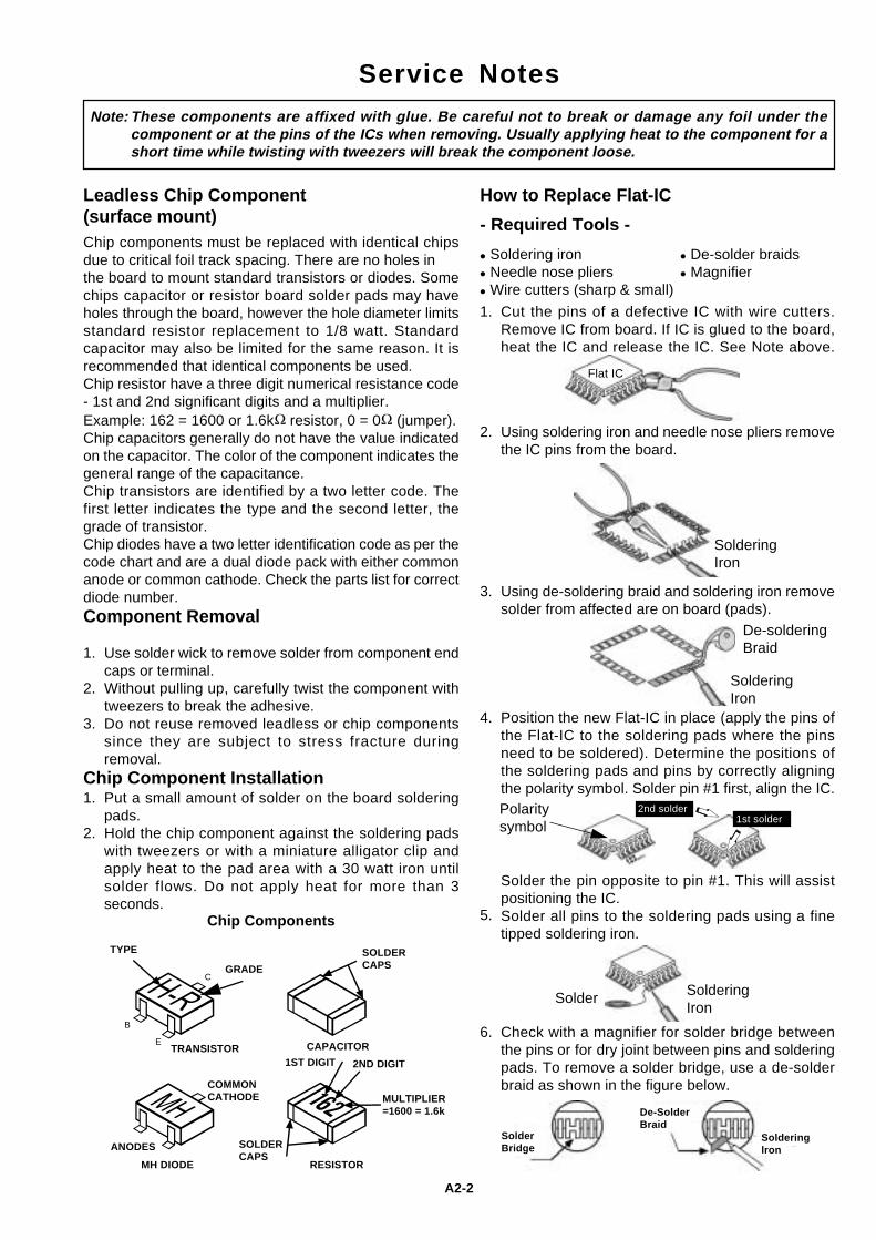
Leadless Chip Component(surface mount)
Service NotesThese components are affixed with glue. Be careful not to break or damage any foil under thecomponent or at the pins of the ICs when removing. Usually applying heat to the component for ashort time while twisting with tweezers will break the component loose.
How to Replace Flat-IC
Note:
Cut the pins of a defective IC with wire cutters.Remove IC from board. If IC is glued to the board,heat the IC and release the IC. See Note above.
Check with a magnifier for solder bridge betweenthe pins or for dry joint between pins and solderingpads. To remove a solder bridge, use a de-solderbraid as shown in the figure below.
Solder the pin opposite to pin #1. This will assistpositioning the IC.Solder all pins to the soldering pads using a finetipped soldering iron.
Position the new Flat-IC in place (apply the pins ofthe Flat-IC to the soldering pads where the pinsneed to be soldered). Determine the positions ofthe soldering pads and pins by correctly aligningthe polarity symbol. Solder pin #1 first, align the IC.
Using de-soldering braid and soldering iron removesolder from affected are on board (pads).
Using soldering iron and needle nose pliers removethe IC pins from the board.
- Required Tools -Chip components must be replaced with identical chipsdue to critical foil track spacing. There are no holes inthe board to mount standard transistors or diodes. Somechips capacitor or resistor board solder pads may haveholes through the board, however the hole diameter limitsstandard resistor replacement to 1/8 watt. Standardcapacitor may also be limited for the same reason. It isrecommended that identical components be used.Chip resistor have a three digit numerical resistance code- 1st and 2nd significant digits and a multiplier.Example: 162 = 1600 or 1.6k resistor, 0 = 0 (jumper).Chip capacitors generally do not have the value indicatedon the capacitor. The color of the component indicates thegeneral range of the capacitance.Chip transistors are identified by a two letter code. Thefirst letter indicates the type and the second letter, thegrade of transistor.Chip diodes have a two letter identification code as per thecode chart and are a dual diode pack with either commonanode or common cathode. Check the parts list for correctdiode number.Component Removal
Chip Components
TYPE
GRADE
TRANSISTOR CAPACITOR
SOLDERCAPS
1ST DIGIT 2ND DIGIT
MULTIPLIER=1600 = 1.6k
SOLDERCAPS
RESISTORMH DIODE
COMMONCATHODE
ANODES
C
B
E
A2-2
Flat IC
SolderingIron
De-solderingBraid
SolderingIron
Polaritysymbol
1st solder
SolderingIron
Solder
SolderBridge
De-SolderBraid
Solderinglron
2nd solder
Use solder wick to remove solder from component endcaps or terminal.Without pulling up, carefully twist the component withtweezers to break the adhesive.Do not reuse removed leadless or chip componentssince they are subject to stress fracture duringremoval.
Chip Component Installation
1.
2.
3.
1.
2.
Put a small amount of solder on the board solderingpads.Hold the chip component against the soldering padswith tweezers or with a miniature alligator clip andapply heat to the pad area with a 30 watt iron untilsolder flows. Do not apply heat for more than 3seconds.
1.
2.
3.
4.
5.
6.
Soldering iron De-solder braids Needle nose pliers Magnifier Wire cutters (sharp & small)
Service Notes (Continued)
IMPORTANT: To protect against possible damage to thesolid state devices due to arcing or static discharge, makecertain that all ground wires and CRT DAG wire aresecurely connected.
CAUTION: The power supply circuit is above earthground and the chassis cannot be polarized. Use anisolation transformer when servicing the Receiver to avoiddamage to the test equipment or to the chassis. Connectthe test equipment to the proper ground ( ) or ( ) whenservicing, or incorrect voltages will be measured.
WARNING: This Receiver has been designed to meetor exceed applicable safety and X-ray radiationprotection as specified by government agencies andindependent testing laboratories.
To maintain original product safety design standardsrelative to X-ray radiation and shock and fire hazard,
parts indicated with the symbol on the schematicmust be replaced with identical parts. Order parts fromthe manufacturer’s parts center using the partsnumbers shown in this service manual, or provide thechassis number and the part reference number.
For optimum performance and reliability, all other partsshould be replaced with components of identicalspecification.
A2-3
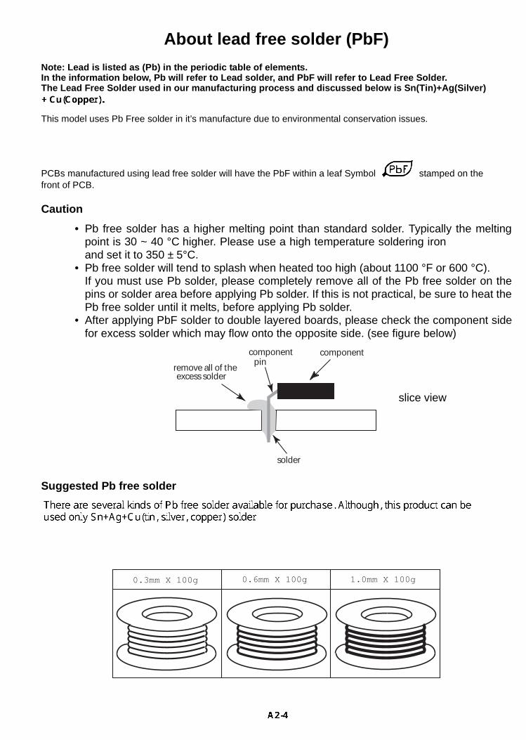
About lead free solder (PbF)
Note: Lead is listed as (Pb) in the periodic table of elements.In the information below, Pb will refer to Lead solder, and PbF will refer to Lead Free Solder.The Lead Free Sold er used in our manuf acturing process and discussed below is Sn(Tin)+Ag (Silver)
This model uses Pb Free solder in it’s manufacture due to environmental conservation issues.
PCBs manufactured using lead free solder will have the PbF within a leaf Symbol stamped on thefront of PCB.
Caution
• Pb free solder has a higher melting point than standard solder. Typically the meltingpoint is 30 ~ 40 °C higher. Please use a high temperature soldering ironand set it to 350 ± 5°C.
• Pb free solder will tend to splash when heated too high (about 1100 °F or 600 °C).If you must use Pb solder, please completely remove all of the Pb free solder on thepins or solder area before applying Pb solder. If this is not practical, be sure to heat thePb free solder until it melts, before applying Pb solder.
• After applying PbF solder to double layered boards, please check the component sidefor excess solder which may flow onto the opposite side. (see figure below)
Suggested Pb free solder
componentcomponentpin
solder
excess solderremove all of the
slice view
0.3mm X 100g 0.6mm X 100g 1.0mm X 100g
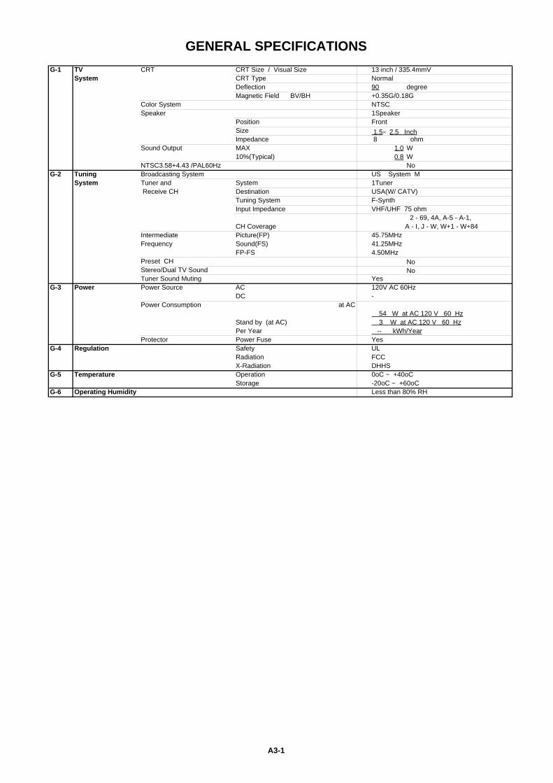
GENERAL SPECIFICATIONS
G-1 TV CRT CRT Size / Visual Size 13 inch / 335.4mmVSystem CRT Type Normal
Deflection 90 degreeMagnetic Field BV/BH +0.35G/0.18G
Color System NTSCSpeaker 1Speaker
Position FrontSize × 1.5 2.5 InchImpedance 8 ohm
Sound Output MAX 1.0 W10%(Typical) 0.8 W
NTSC3.58+4.43 /PAL60Hz NoG-2 Tuning Broadcasting System US System M
System Tuner and System 1Tuner Receive CH Destination USA(W/ CATV)
Tuning System F-SynthInput Impedance VHF/UHF 75 ohm
2 - 69, 4A, A-5 - A-1, CH Coverage A - I, J - W, W+1 - W+84
Intermediate Picture(FP) 45.75MHzFrequency Sound(FS) 41.25MHz
FP-FS 4.50MHzPreset CH NoStereo/Dual TV Sound NoTuner Sound Muting Yes
G-3 Power Power Source AC 120V AC 60HzDC -
Power Consumption at AC 54 W at AC 120 V 60 Hz
Stand by (at AC) 3 W at AC 120 V 60 HzPer Year -- kWh/Year
Protector Power Fuse YesG-4 Regulation Safety UL
Radiation FCC X-Radiation DHHS
G-5 Temperature Operation 0oC ~ +40oCStorage -20oC ~ +60oC
G-6 Operating Humidity Less than 80% RH
A3-1
GENERAL SPECIFICATIONS
G-7 On Screen Menu YesDisplay Menu Type Picture(Matsusita Type)
Picture YesContrast(Picture) YesBrightness YesColor YesTint YesSharpness YesNormal Yes
Audio NoBass NoTreble NoBalance NoBBE On/Off NoStable Sound On/Off No
SET UP YesLanguage YesMode YesAuto Program YesManual Program YesCC Yes
Timer YesLock YesExit Yes
CH Label NoFavorite CH NoColor Stream DVD/DTV No
Control Level YesSound YesBrightness YesContrast(Picture) YesColor YesTint YesSharpness YesTuning NoBass NoTreble NoBalance NoBack Light No
Stereo,Audio Output,SAP NoVideo(Aux) YesColor Stream NoChannel(TV/Cable) YesCH Label NoSound Mute YesV-chip Rating Yes
G-8 OSD Language English French Spanish
G-9 Clock and Sleep Timer Max Time 120 Min Timer Step 10 Min
On/Off Timer Program(On Tim / Off Tim) NoWake Up Timer NoTimer Back-up (at Power Off Mode) more than -- Min Sec
A3-2
GENERAL SPECIFICATIONS
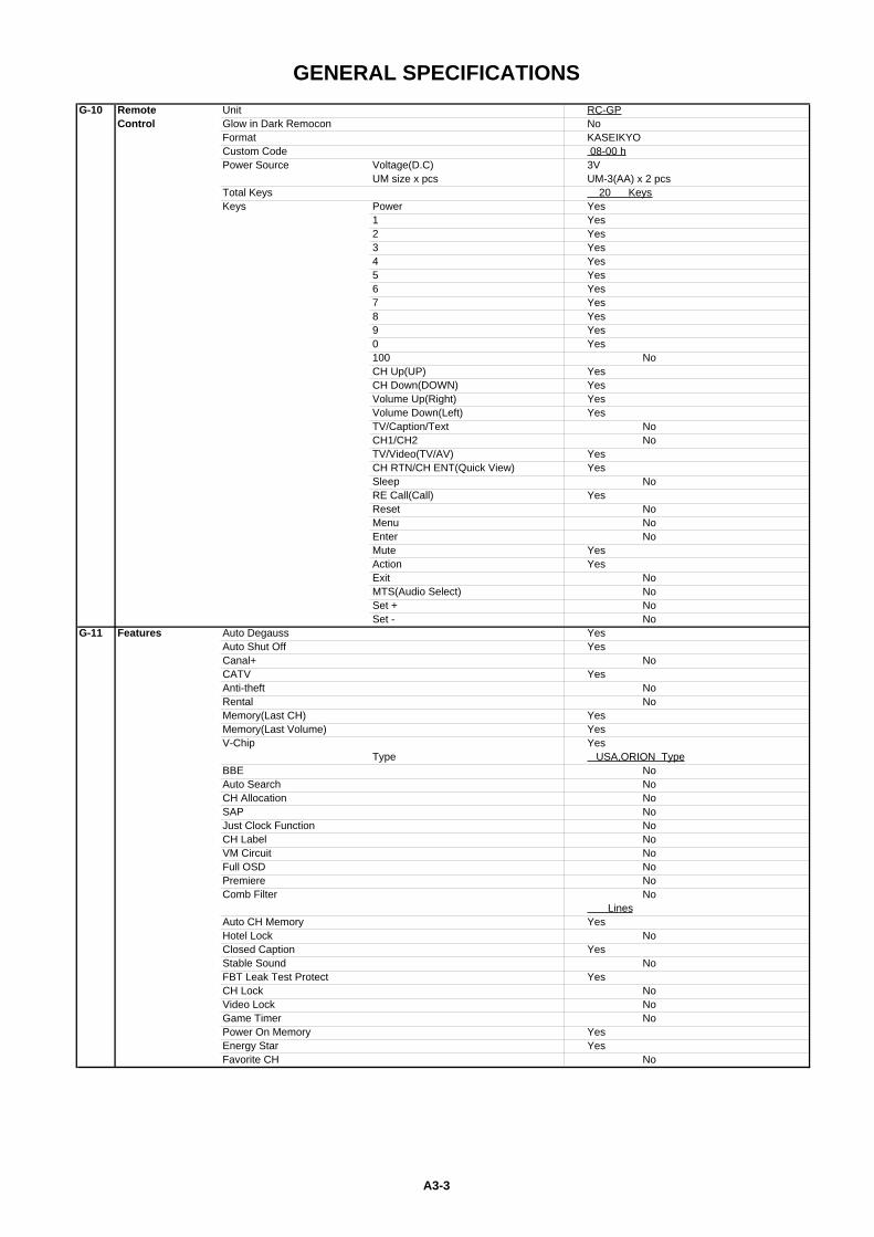
G-10 Remote Unit RC-GPControl Glow in Dark Remocon No
Format KASEIKYOCustom Code 08-00 hPower Source Voltage(D.C) 3V
UM size x pcs UM-3(AA) x 2 pcs Total Keys 20 KeysKeys Power Yes
1 Yes2 Yes3 Yes4 Yes5 Yes6 Yes7 Yes8 Yes9 Yes0 Yes100 NoCH Up(UP) YesCH Down(DOWN) YesVolume Up(Right) YesVolume Down(Left) YesTV/Caption/Text NoCH1/CH2 NoTV/Video(TV/AV) YesCH RTN/CH ENT(Quick View) YesSleep NoRE Call(Call) YesReset NoMenu NoEnter NoMute YesAction YesExit NoMTS(Audio Select) NoSet + NoSet - No
G-11 Features Auto Degauss YesAuto Shut Off YesCanal+ NoCATV YesAnti-theft NoRental NoMemory(Last CH) YesMemory(Last Volume) YesV-Chip Yes
Type USA,ORION TypeBBE NoAuto Search NoCH Allocation NoSAP NoJust Clock Function NoCH Label NoVM Circuit NoFull OSD NoPremiere NoComb Filter No
LinesAuto CH Memory YesHotel Lock NoClosed Caption YesStable Sound NoFBT Leak Test Protect YesCH Lock NoVideo Lock NoGame Timer NoPower On Memory YesEnergy Star YesFavorite CH No
A3-3
GENERAL SPECIFICATIONS
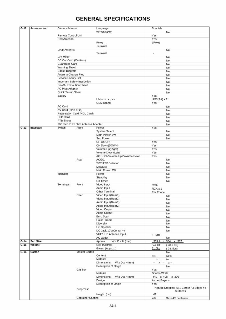
G-12 Accessories Owner's Manual Language SpanishW/ Warranty No
Remote Control Unit YesRod Antenna Yes
Poles 1PolesTerminal
Loop Antenna NoTerminal -
U/V Mixer NoDC Car Cord (Center+) NoGuarantee Card NoWarning Sheet NoCircuit Diagram NoAntenna Change Plug NoService Facility List NoImportant Safety Instruction NoDew/AHC Caution Sheet NoAC Plug Adapter NoQuick Set-up Sheet NoBattery Yes
UM size x pcs UM3(AA) x 2OEM Brand Yes
AC Cord NoAV Cord (2Pin-1Pin) NoRegistration Card (NDL Card) NoESP Card NoPTB Sheet No300 ohm to 75 ohm Antenna Adapter No
G-13 Interface Switch Front Power YesSystem Select No Main Power SW No Sub Power No CH Up(UP) YesCH Down(DOWN) YesVolume Up(Right) YesVolume Down(Left) YesACTION=Volume Up+Volume Down Yes
Rear AC/DC No TV/CATV Selector No Degauss No Main Power SW No
Indicator Power NoStand-by No On Timer No
Terminals Front Video Input RCA Audio Input RCA x 1 Other Terminal Ear Phone
Rear Video Input(Rear1) NoVideo Input(Rear2) NoAudio Input(Rear1) No Audio Input(Rear2) No Video Output NoAudio Output No Euro Scart NoColor Stream NoDiversity NoExt Speaker NoDC Jack 12V(Center +) NoVHF/UHF Antenna Input F TypeAC Outlet No
G-14 Set Size Approx. W x D x H (mm) 359.4 x 354 x 337 G-15 Weight Net (Approx.) 9.5 kg ( 20.9 lbs)
Gross (Approx.) 11.0kg ( 24.4lbs)G-16 Carton Master Carton No
Content ---- SetsMaterial -- /--Dimensions W x D x H(mm) -- x -- x -- Description of Origin No
Gift Box YesMaterial Double/WhiteDimensions W x D x H(mm) 440 x 408 x 396 Design As per Buyer'sDescription of Origin Yes
Drop Test Natural Dropping At 1 Corner / 3 Edges / 6Surfaces
Height (cm) 62 Container Stuffing 725 Sets/40' container
A3-4
GENERAL SPECIFICATIONS
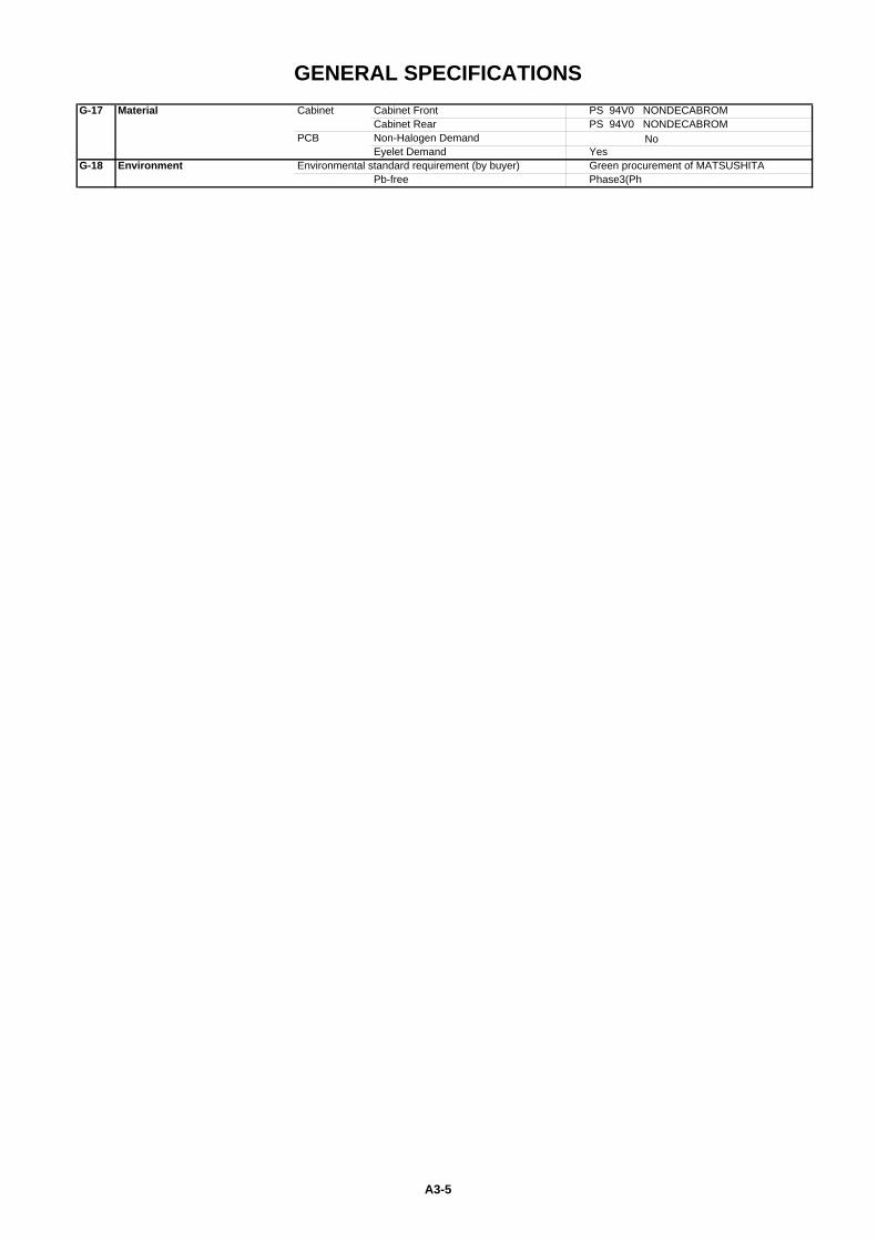
G-17 Material Cabinet Cabinet Front PS 94V0 NONDECABROM Cabinet Rear PS 94V0 NONDECABROM
PCB Non-Halogen Demand NoEyelet Demand Yes
G-18 Environment Environmental standard requirement (by buyer) Green procurement of MATSUSHITAPb-free Phase3(Ph
A3-5

1. REMOVAL OF ANODE CAPRead the following NOTED items before starting work.
After turning the power off there might still be a potentialvoltage that is very dangerous. When removing theAnode Cap, make sure to discharge the Anode Cap'spotential voltage.Do not use pliers to loosen or tighten the Anode Capterminal, this may cause the spring to be damaged.
*
*
REMOVAL
1. Follow the steps as follows to discharge the Anode Cap.Connect one end of an Alligator Clip to the metal part of aflat-blade screwdriver and the other end to ground.While holding the plastic part of the insulated Screwdriver,touch the support of the Anode with the tip of theScrewdriver.A cracking noise will be heard as the voltage is discharged.
Flip up the sides of the Rubber Cap in the direction of thearrow and remove one side of the support.
2.
DISASSEMBLY INSTRUCTIONS
3. After one side is removed, pull in the opposite direction toremove the other.
NOTE
Take care not to damage the Rubber Cap.
INSTALLATION
1. Clean the spot where the cap was located with a smallamount of alcohol.
Location of Anode Cap
NOTE
Confirm that there is no dirt, dust, etc. at the spot wherethe cap was located.
2.
3.
Arrange the wire of the Anode Cap and make sure thewire is not twisted.Turn over the Rubber Cap.
4. Insert one end of the Anode Support into the anode button,then the other as shown in the figure below.
5.6.
Confirm that the Support is securely connected.Put on the Rubber Cap without moving any parts.
B-1
GND on the CRT
Screwdriver
Alligator Clip
SupportCRT
GND on the CRT
Rubber Cap
CRTSupport
CRTSupport
2. NOTE FOR THE REMOVAL OF THEMAIN PCBWhen the removal of the Main PCB, remove the hookfirst, then draw it in the direction of the arrow.
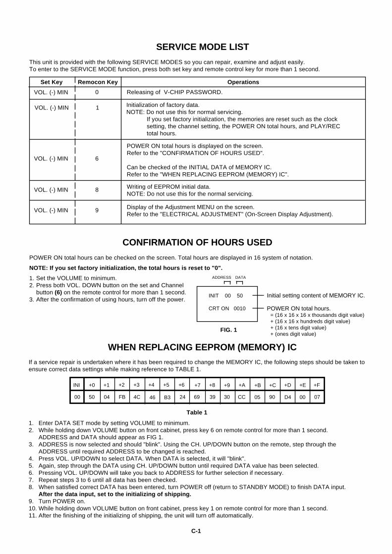
SERVICE MODE LIST
This unit is provided with the following SERVICE MODES so you can repair, examine and adjust easily.To enter to the SERVICE MODE function, press both set key and remote control key for more than 1 second.
Set Key Remocon Key Operations
VOL. (-) MIN 1 Initialization of factory data.NOTE: Do not use this for normal servicing. If you set factory initialization, the memories are reset such as the clock
setting, the channel setting, the POWER ON total hours, and PLAY/REC total hours.
VOL. (-) MIN 6
POWER ON total hours is displayed on the screen.Refer to the "CONFIRMATION OF HOURS USED".
Can be checked of the INITIAL DATA of MEMORY IC.Refer to the "WHEN REPLACING EEPROM (MEMORY) IC".
VOL. (-) MIN 8 Writing of EEPROM initial data.NOTE: Do not use this for the normal servicing.
VOL. (-) MIN Display of the Adjustment MENU on the screen.Refer to the "ELECTRICAL ADJUSTMENT" (On-Screen Display Adjustment).
9
CONFIRMATION OF HOURS USED
POWER ON total hours can be checked on the screen. Total hours are displayed in 16 system of notation.
NOTE: If you set factory initialization, the total hours is reset to "0".
1.2.
3.
Set the VOLUME to minimum.Press both VOL. DOWN button on the set and Channelbutton (6) on the remote control for more than 1 second.After the confirmation of using hours, turn off the power.
FIG. 1
Initial setting content of MEMORY IC.
POWER ON total hours. = (16 x 16 x 16 x thousands digit value) + (16 x 16 x hundreds digit value) + (16 x tens digit value) + (ones digit value)
ADDRESS DATA
INIT 00 50
CRT ON 0010
VOL. (-) MIN 0 Releasing of V-CHIP PASSWORD.
WHEN REPLACING EEPROM (MEMORY) IC
If a service repair is undertaken where it has been required to change the MEMORY IC, the following steps should be taken toensure correct data settings while making reference to TABLE 1.
Table 1
+9+2INI +0 +1 +3 +4 +5 +6 +7
00
+8 +A
46 B3 24 69 39 30 CC50 04 FB 4C
+B +C +D +E +F
05 90 D4 00 07
1.2.
3.
4.5.6.7.8.
9.10.11.
Enter DATA SET mode by setting VOLUME to minimum.While holding down VOLUME button on front cabinet, press key 6 on remote control for more than 1 second.ADDRESS and DATA should appear as FIG 1.ADDRESS is now selected and should "blink". Using the CH. UP/DOWN button on the remote, step through theADDRESS until required ADDRESS to be changed is reached.Press VOL. UP/DOWN to select DATA. When DATA is selected, it will "blink".Again, step through the DATA using CH. UP/DOWN button until required DATA value has been selected.Pressing VOL. UP/DOWN will take you back to ADDRESS for further selection if necessary.Repeat steps 3 to 6 until all data has been checked.When satisfied correct DATA has been entered, turn POWER off (return to STANDBY MODE) to finish DATA input.After the data input, set to the initializing of shipping.Turn POWER on.While holding down VOLUME button on front cabinet, press key 1 on remote control for more than 1 second.After the finishing of the initializing of shipping, the unit will turn off automatically.
C-1
ELECTRICAL ADJUSTMENTS
D-1
1.
Read and perform these adjustments when repairing thecircuits or replacing electrical parts or PCB assemblies.
CAUTION
•
•
•
•
•
Use an isolation transformer when performing any serviceon this chassis.Before removing the anode cap, discharge electricitybecause it contains high voltage.When removing a PCB or related component, afterunfastening or changing a wire, be sure to put the wireback in its original position.When you exchange IC and Transistor with a heat sink,apply silicon grease (YG6260M) on the contractsection of the heat sink, Before applying new silicongrease, remove all the old silicon grease. (Old greasemay cause damages to the IC and Transistor.)The adjustments are needed for each mode, RF mode andAV mode. Perform the adjustments refering each adjust-ment items.
2. BASIC ADJUSTMENTSBEFORE MAKING ELECTRICALADJUSTMENTS 2-1: CUT OFF (RF)
1.
2.3.
4.
Adjust the unit to the following settings.R.DRIVE=10, B.DRIVE=10, R.BIAS=64, G.BIAS=64,B.BIAS=64, BRI.CENT=120, CONT.MAX=40.Place the set in Aging Test for more than 15 minutes.Activate the adjustment mode display of Fig. 1-1 andpress the channel button (01) on the remote control toselect "CUT OFF".Adjust the Screen Volume until a dim raster is obtained.
2-2: FOCUS (RF)
1.2.3.
Receive a broadcast.Turn the Focus Volume fully counterclockwise once.Adjust the Focus Volume until picture is distinct.
2-3: WHITE BALANCE (RF)
NOTE: Adjust after performing CUT OFF adjustment.
Place the set in Aging Test for more than 10 minutes.Receive the white 100% signal from the PatternGenerator.Using the adjustment control, set the brightness andcontrast to normal position.Activate the adjustment mode display of Fig. 1-1 andpress the channel button (10) on the remote control toselect "R.BIAS".Using the VOL. UP/DOWN button on the remote control,adjust the R.BIAS.Press the CH. UP/DOWN button on the remote control toselect the "R.DRIVE", "B.DRIVE", "G.BIAS" or "B.BIAS".Using the VOL. UP/DOWN button on the remote control,adjust the R.DRIVE, B.DRIVE, G.BIAS or B.BIAS.Perform the above adjustments 6 and 7 until the whitecolor is achieved.
1.2.
3.
4.
5.
6.
7.
8.
1. Synchro Scope2. Digital Voltmeter
On-Screen Display Adjustment
In the condition of NO indication on the screen.Press the VOL. DOWN button on the set and theChannel button (9) on the remote control for more than1 second to appear the adjustment mode on the screenas shown in Fig. 1-1.
1.
Fig. 1-1
Use the Channel UP/DOWN button or Channel button(0-9) on the remote control to select the options shownin Fig. 1-2.Press the ACTION button on the remote control to endthe adjustments.
2.
3.
Prepare the following measurement tools for electricaladjustments.
FUNCTIONOSD HCUT OFFH.VCOH.PHASEV.SIZEV.SHIFTR.DRIVEB.DRIVER.BIASG.BIASB.BIASBRIGHT CENT
NO.000104050607080910111213
Fig. 1-2
FUNCTIONBRIGHT MAXBRIGHT MINCONTRAST CENTCONTRAST MAXCONTRAST MINCOLOR CENTCOLOR MAXCOLOR MINTINTSHARPNESSTEST MONOTEST STEREO
NO.141516171819202122232829
TV
00 OSD 19
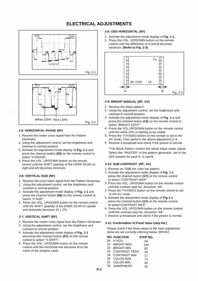
2-4: SUB TINT/SUB COLOR (RF, AV)
1.2.3.
4.
5.6.
7.
8.9.
Receive the color bar pattern. (RF Input)Connect the oscilloscope to TP023.Activate the adjustment mode display of Fig. 1-1 andpress the channel button (22) on the remote control toselect "TINT".Press the VOL. UP/DOWN button on the remote controluntil the section "A" becomes as straight line.(Refer to Fig. 2-1)Connect the oscilloscope to TP022.Activate the adjustment mode display of Fig. 1-1 andpress the channel button (19) on the remote control toselect "COLOR CENT".Press the VOL. UP/DOWN button on the remote controluntil the red color level is adjusted to 110 ±10% of thewhite level. (Refer to Fig. 2-2)Receive the color bar pattern. (Audio Video Input)Press the TV/VIDEO button on the remote control to set to the AV mode. Then perform the above adjustments2~7.
ELECTRICAL ADJUSTMENTS
D-2
2-8: OSD HORIZONTAL (RF)
1.2.
Activate the adjustment mode display of Fig. 1-1.Press the VOL. UP/DOWN button on the remotecontrol until the difference of A and B becomesminimum. (Refer to Fig. 2-3)
BA
TV
00 OSD 19
Fig. 2-3
Receive the black pattern*.Using the adjustment control, set the brightness andcontrast to normal position.Activate the adjustment mode display of Fig. 1-1 andpress the channel button (13) on the remote control toselect "BRIGHT CENT".Press the VOL.UP/DOWN button on the remote controluntil the white 10% is starting to be visible.Press the TV/VIDEO button on the remote to set to theAV mode. Then perform the above adjustment 2~4.Receive a broadcast and check if the picture is normal.
1.2.
3.
4.
5.
6.
2-9: BRIGHT MANUAL (RF, AV)
Fig. 2-1
Fig. 2-2
2-5: HORIZONTAL PHASE (RF)
1.
2.
3.
4.
Receive the center cross signal from the PatternGenerator.Using the adjustment control, set the brightness andcontrast to normal position.Activate the adjustment mode display of Fig. 1-1 andpress the channel button (05) on the remote control toselect "H.PHASE".Press the VOL. UP/DOWN button on the remotecontrol until the SHIFT quantity of the OVER SCAN onright and left becomes minimum.
2-6: VERTICAL SIZE (RF)
1.2.
3.
4.
Receive the cross hatch signal from the Pattern Generator.Using the adjustment control, set the brightness andcontrast to normal position.Activate the adjustment mode display of Fig. 1-1 andpress the channel button (06) on the remote control toselect "V.SIZE".Press the VOL. UP/DOWN button on the remote controluntil the SHIFT quantity of the OVER SCAN on upsideand downside becomes 10 ± 2%.
2-7: VERTICAL SHIFT (RF)
1.2.
3.
4.
Receive the center cross signal from the Pattern Generator.Using the adjustment control, set the brightness andcontrast to normal position.Activate the adjustment mode display of Fig. 1-1and press the channel button (07) on the remotecontrol to select "V.SHIFT".Press the VOL. UP/DOWN button on the remotecontrol until the horizontal line becomes fit to thenotch of the shadow mask.
White 100% Red 110%
"A"
Receive an 70dB the color bar pattern.Activate the adjustment mode display of Fig. 1-1press the channel button (17) on the remote controlto select "CONTRAST MAX".Press the VOL. UP/DOWN button on the remote controluntil the contrast step No. becomes "44".Press the TV/VIDEO button on the remote control to set to the AV mode.Activate the adiustment mode display of Fig 1-1press the channel button (17) on the remote controlto select"CONTRAST MAX".Press the VOL.UP/DOWN button on the remote controlunitil the contrast step No. becomes "48".Receive a broadcast and check if the picture is normal.
1.2.
3.
4.
5.
6.
7.
2-10: SUB CONTRAST (RF, AV)
Please check if the fixed values of the each adjustmentitems are set correctly referring below. (RF/AV)
2-11: Confirmation of Fixed Value (step No.)
NO.0414151618202123
FUNCTIONH VCOBRIGHT MAXBRIGHT MINCONTRAST CENTCONTRAST MINCOLOR MAXCOLOR MINSHARPNESS
STEP NO.
*The Black Pattern means the whole black raster signal.Select the "RASTER" of the pattern generator, set to theOFF position for each R, G and B.
04140603017740040
ELECTRICAL ADJUSTMENTS
D-3
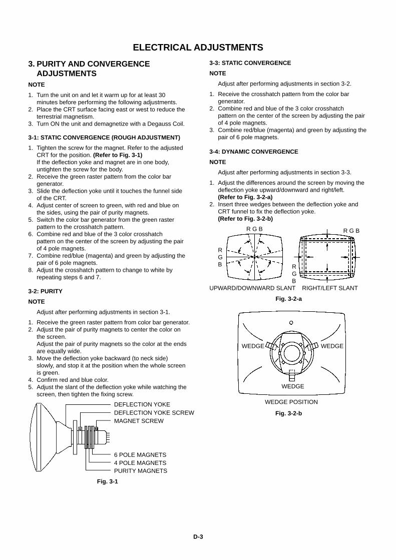
3. PURITY AND CONVERGENCEADJUSTMENTS
NOTE
1.
2.
3.
Turn the unit on and let it warm up for at least 30minutes before performing the following adjustments.Place the CRT surface facing east or west to reduce theterrestrial magnetism.Turn ON the unit and demagnetize with a Degauss Coil.
3-1: STATIC CONVERGENCE (ROUGH ADJUSTMENT)
1.
2.
3.
4.
5.
6.
7.
8.
Tighten the screw for the magnet. Refer to the adjustedCRT for the position. (Refer to Fig. 3-1)If the deflection yoke and magnet are in one body,untighten the screw for the body.Receive the green raster pattern from the color bargenerator.Slide the deflection yoke until it touches the funnel sideof the CRT.Adjust center of screen to green, with red and blue onthe sides, using the pair of purity magnets.Switch the color bar generator from the green rasterpattern to the crosshatch pattern.Combine red and blue of the 3 color crosshatchpattern on the center of the screen by adjusting the pairof 4 pole magnets.Combine red/blue (magenta) and green by adjusting thepair of 6 pole magnets.Adjust the crosshatch pattern to change to white byrepeating steps 6 and 7.
3-2: PURITY
NOTE
Adjust after performing adjustments in section 3-1.
1.2.
3.
4.5.
Receive the green raster pattern from color bar generator.Adjust the pair of purity magnets to center the color onthe screen.Adjust the pair of purity magnets so the color at the endsare equally wide.Move the deflection yoke backward (to neck side)slowly, and stop it at the position when the whole screenis green.Confirm red and blue color.Adjust the slant of the deflection yoke while watching thescreen, then tighten the fixing screw.
DEFLECTION YOKEDEFLECTION YOKE SCREWMAGNET SCREW
6 POLE MAGNETS4 POLE MAGNETSPURITY MAGNETS
Fig. 3-1
3-3: STATIC CONVERGENCE
NOTE
Adjust after performing adjustments in section 3-2.
1.
2.
3.
Receive the crosshatch pattern from the color bargenerator.Combine red and blue of the 3 color crosshatchpattern on the center of the screen by adjusting the pairof 4 pole magnets.Combine red/blue (magenta) and green by adjusting thepair of 6 pole magnets.
3-4: DYNAMIC CONVERGENCE
NOTE
Adjust after performing adjustments in section 3-3.
1.
2.
Adjust the differences around the screen by moving thedeflection yoke upward/downward and right/left.(Refer to Fig. 3-2-a)Insert three wedges between the deflection yoke andCRT funnel to fix the deflection yoke.(Refer to Fig. 3-2-b)
R G B
RGB R
GB
R G B
UPWARD/DOWNWARD SLANT RIGHT/LEFT SLANT
Fig. 3-2-a
WEDGE WEDGE
WEDGE
WEDGE POSITION
Fig. 3-2-b
ELECTRICAL ADJUSTMENTS
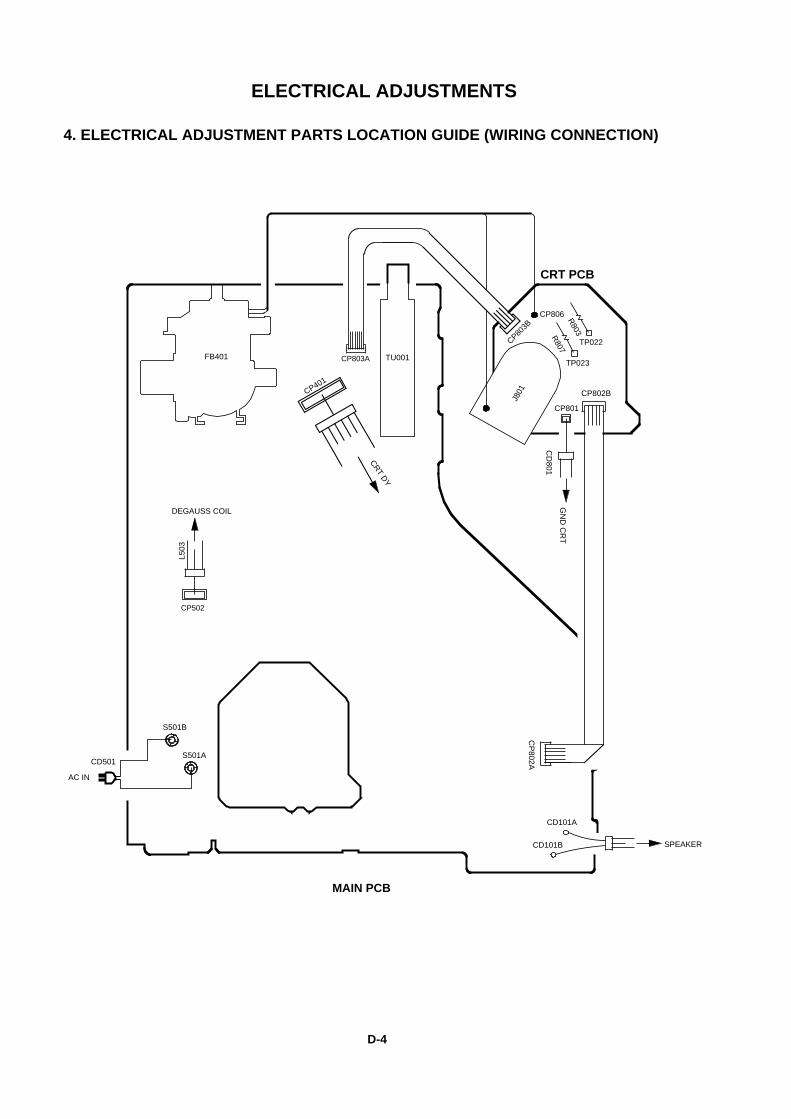
4. ELECTRICAL ADJUSTMENT PARTS LOCATION GUIDE (WIRING CONNECTION)
CD101A
CP
802A
TU001
S501A
S501B
FB401
CD101B
AC IN
CP401
CP802B
CP806
CP803B
CP801
R807
R803
SPEAKER
TP023
TP022
CRT PCB
MAIN PCB
GN
D C
RT
CD
801
DEGAUSS COIL
CP502
L503
CR
T DY
D-4
CP803A
J801
CD501

OSD
BLOCK DIAGRAM
74
78
70
69
68
67
73
66 ATTRGB Proc.2OSD SWCONTRAST BRIGHTNESS
I/OIICTIMINT
PWMAD
MCUCLK
VCXO
RGB OUTPUT Stage DRIVE CUT OFF HV BLK
Ver.Proc.Ver SYNC SEPVer.COUNT DOWNV RAMP
2021
IC1001 AN7511
Q801
RED OUT
Q802
GREEN OUT
Q803
BLUE OUT
Q402
H. DRIVE
Q401
H. OUTPUT
2 6
SOUND AMPIC4 8
Q607
H-CTL
SPEAKERSP1001
52
51
50
34
45
46
9
HV
F
S
FB401
10
1
2
3
CRTV801
3 9 7
RGB
Heater
F 84
PUMP UP
AMP+
-
7 53 6
V-OUT ICIC401 AN5522
VCC
RGB Proc.1RGB MATRIXCOLOR CONT
ROMRAM
38372627575856 16
Hor.Proc.SYNC SEPA/Hor. VCOHor.COUNT DOWNAFC-1/H COINCIDENTAFC-2 H PHASE
1
J703
2
J702
2
DYD501~D504
RECTIFIER
31
42L501
AC IN
F501
Q507
FEED BACK
T502
4
8
13
FEED BACKSW
Q502
BUFFER
Q501
POWER AMP
6
DEGAUSS COILL503
65MEMORY ICIC199 BR24L02F-WE2
SDA SCL
POWER
VOL. DOWN
CH. DOWN
VOL. UP
CH. UP
X6013.579545MHz
TU001
10 1311 12 17
OS101
1
16
Q505
Q503
PROTECT DRV.
MICON/CHROM ICIC101 OEC7094B
Chroma Proc.ACC/C-BPFAPC/KILLERTINT/DEMO
P. FAIL
IC501LTV-817M-VB
1
3
2EAR PHONE_JACKJ1001
E-1 E-2
TM
C573C
TCC434C
Q602
Q606
R605
D604
D603
C621
C620_1
W803
C1003
IC1001
C1005
C1001
W813
W032W031
W036
L001
D001
R602
W053
W054
C616
C615
D608
D609
D607
W046
R608
R621
R604
D606
R606
W048
Q607C633
R616
R617
R109
IC199_1
Q601Q603
D102
D101
W040
R615
R613R614
R611
C628
W051
D605
C605
R601
X601
C601C106
W041
C614
W060
CP
802A
CD
101A
CD
101B
C612
R701
J703
J702
TU
001
R002
SW101 SW102 SW103 SW104 SW105
R516
Q505R505
R449
R448
R413
W038
W039
C427
R416
D403
R415
R418
R424
C414
J1001
R629
IC40
1
W027
W001
C437
R408_1
D412
D509
D508
HS501
C513_1
C508
TH501_1
C511
C526_1
C519
C446
C417
W005
W826
W020
R814C810_1
R816
R809
R811
R813C808_1
R815
R504
TP024
TP023
TP022
TP401
R519
R509
D512
R429
FH
501
FH502
F501
S501B
CP801
R806
R802
L501
CP803B
L801
R805_
1
R80
3_1
R80
7_1
CP806
Q802
CP802B
S501A
C435
R518_1
R502
D515
W006
IC501
D511
R515 R513
D528
R512
D516
R447
CP401
R507
CP803A
C403
R514
C410_1
R427
D501
HS402
R520
C509
R506
R503
Q502
R508
Q501
R542
D503D
502
CP502
D408
D405
B504
B501
R51
7_1
D504
R422
D510
D513
D505
D506
R1007
D410
R410
AF
C
HS401
C123
OS101
J801
CO
L
+B
8V
AB
L
GN
D
25V
12V180V
HE
AT
ER
FB401
R423
R538
D524
W003
Q801
Q803D
411
C434
C401
L401
W802
Q507
W035
R417C516
R525
Q503W049
C507
D514
R523
R527
R607
W037
D521
C622
W061
C610
W052
R530
Q511
W050
C617
W816
W028
R405
C809_1D
404
W007
W008
W029
D522
R001
R445
W042
R528
D701
D610
R1001
C1006
Q509 D520
R130
C521_1
R510_1
W817
W026
C103
C606
W014
W012
C002
C118
Q401
W011
W004
CP601
W043
W044
W045
W018
R110
R113
R112
W057
W058
C602
C004
W062
W059
W023
W017
W030
W022
R421
C440
R446
R403
W033W068
C448_1
C624_1
C630
D406
D409
C634_1
W067
W064
R120_1
W070
W019
R401_1
R409_1
W010
W009
C007
W024
W065
W069
R119
W071
R804_1
C406
T401
R620
R404
Q402
C518
T502
C510
C422
C502
C503
C505
R501
C515
C514_1
C517_1
C418
C506
C819_1
CP503
C443
W072
Q510
W073
W025
W034
W015
R603
R537
C623
C420_1
D601
W055
D703
D602
W056
W066
D704
D705
R704
D702
D612
D523
C1007
R500
W828
W823
W808
W831
D413
W811
W809
S803Y
S803X
C423
W810
W832
W830
W819
W827
CD
501
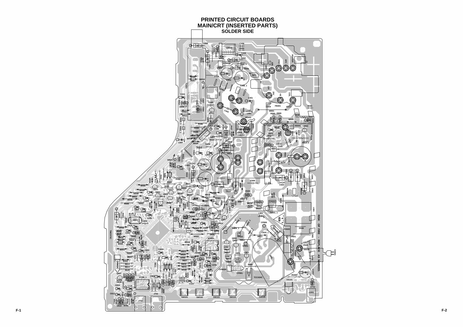
PRINTED CIRCUIT BOARDSMAIN/CRT (INSERTED PARTS)
SOLDER SIDE
F-1 F-2
RIS
KO
FF
IRE
-R
EP
LA
CE
AS
MA
RK
ED
.
1
25
41
64
TM
C57
3C
TC
C43
4C
C1004_2
R10
03R004R003
R610
C10
1
C60
9
R61
8
C11
2
C62
9
C62
6C
627
C60
4
C104C102
IC10
1
R702
R70
3
R128
R12
6
R101
R14
3
R10
08
R420
R41
9C501_2
C60
3
R104C10
8_1
C10
7
C10
5R
102
R10
3
R533
R12
5
R535
R534
C113_1
R609
R11
5
C001
R10
05
R10
04
R122
R12
7
R11
6
R627
R12
4R
106
R105
R10
7
R108
R129
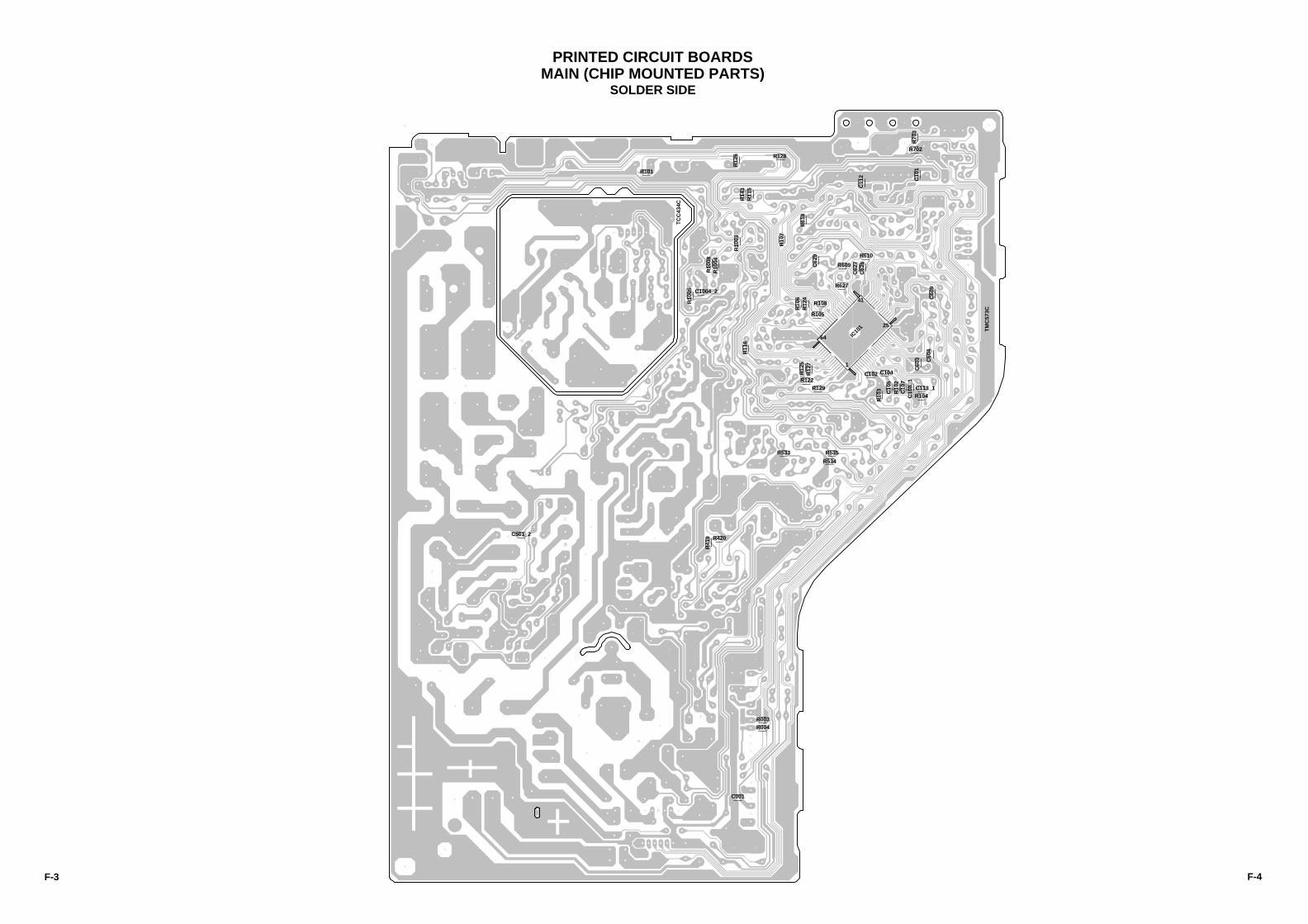
PRINTED CIRCUIT BOARDSMAIN (CHIP MOUNTED PARTS)
SOLDER SIDE
F-3 F-4

A B C D E F G H
A B C D E F G H
2
1
3
4
5
6
7
8
2
1
3
4
5
6
7
8
AUDIO SIGNAL
WAS RECEIVED IN GOOD CONDITION AND PICTURE IS NORMAL.WITH THE DIGITAL TESTER WHEN THE COLOR BROADCAST
NOTE:THE DC VOLTAGE AT EACH PART WAS MEASURED
C001
0.01 F
C624
_1 163
VM
KT
C626
0.01
F
C627
0.01
F
C629
0.01F
C112
100P
CH
C602
0.1
F
C104
0.01
F
C108
_1
0.00
1B
C113
_1
560P
BC102
0.01 F
C101
0.01 F
C004
0.02
2F
C620_1
0.01 B
C105
470P
B
C107
220P
B
C609
0.01 FC6
04
0.02
2F
C603
22P
CH
C007
0.02
2B
C634_1
0.0056 B
C002
10006.3V YK
C628 1
50V
KA
C623
2.250V KA
C630
47010VYK
C616
150V KA
C106
150
VKA
C103
4725
VYK
C617
10010V YK
C118
1006.3V KA
C633
1050
VKA
C606 10
010
VYK
C123
1025
VKA
C622
150V KA
C614
150V KA C612
150V KA
C621
4725V YK
C610
476.3V KAC6
05
150
VKA
C601 1
50V
KAC615
150V KA
R618
22K
R106
4.7K
R130
10K 1/4W
R108 100
R107 100
R105
4.7K
R617
47K
1/4W
R611
10K
1/4W
R609
120K
R604
100 1/4W
R120
_1
470
1/4W
R116 2.2K
R115 22K
R613
100
1/4W
R614
100
1/4W
R102 1K
R602
1001
/4W
R603
120 1/2W
R605
220 1/2W
R606
22K 1/4W
R610
6.8K
R607
100 1/4W
R615
100
1/4W
R126
2.7K
R101
560
R122
10K
R109
10K 1/4W
R621
220 1/4W
R608
1K 1/4W
R620
2.2K
1/2W
R143
47
R001
15K 1/2W
R002
15K 1/2W
R003
100
R004
100
R104
1M
R128
560
R127
1K
R627
10K
R124
10K
R125
47K
R129
47K
R119
22K 1/4W
R103
1K
R601
8.2K
1/4W
R110
10K 1/4W
R112 2.2K 1/4W
R113 2.2K 1/4W
R616
1K1/
4W
OF PRINTING AND SUBJECT TO CHANGE WITHOUT NOTICENOTE:THIS SCHEMATIC DIAGRAM IS THE LATEST AT THE TIME
DANS LA NOMENCLATURE DES PIECESN’UTILISER QUE CELLS DECRITESDANGEREUSES AN POINT DE VUE SECURITE
:LES PIECES REPAREES PAR UN ETANTATTENTION:SINCE THESE PARTS MARKED BYCAUTIONDESCRIBED IN PARTS LIST ONLYCRITICAL FOR SAFETY,USE ONES
ARE
W82
3
W80
8
W82
8
W80
9
W81
6
IC19
9_1
BR24
L02F
-WE2
MEM
ORY
IC
1 2 3 4
5678
TUNER VIDEO SIGNAL
D607
MTZ
J9.1
B
D608
MTZ
J9.1
B
D609
MTZ
J9.1
B
D605
MTZJ9.1B
D610
MTZJ6.8B
D102
MTZ
J5.6
B
D001
MTZ
J33B
D101
MTZ
J5.6
B
D604
MTZJ8.2B
D602
MTZJ9.1B
D601
MTZJ6.8B
DEFLECTION SIGNALB.SIGNALG.SIGNALR.SIGNAL
D612
1SS1
33
D603
1SS133
D606
11E1
-EIC
Q606KTC3203_Y
8V REG
Q601KTC3203_Y
5V REG
Q602KTC3203_Y
5V REG
Q603KTC3203_Y
5V REG
Q607
KTC3198
H.CTL
R629
22 3W
IC101OEC7094B
MICON/CHROMA IC
1 10 11 12 13 14 15 16 17 18 192 20 21 22 23 24
2526
2728
29
3
3031
3233
3435
3637
3839
4
40
414243444546474849
5
50515253545556575859
6
6061626364
6566
6768
69
7
7071
7273
7475
7677
7879
8
80
9
SW10
4EV
Q215
05R
VOL
DOW
N
SW10
3EV
Q215
05R
VOL
UP
SW10
2EV
Q215
05R
CH D
OWN
SW10
1EV
Q215
05R
CH U
P
SW10
5EV
Q215
05R
POW
ER
X601
100C
T3R5
053.
5795
45M
Hz
CP601A2001WR2-6P
1
2
3
4
5
6
L001
3.3uH 0305
VoutB+ GN
D
OS101RPM7137-WH5
123
TU001ENG36A29GF
1
10
11
12
13
14
15
16
17
1819
2
20 21
3
4
5
6
7
8
9
S803X
P.CO
N+5V
P.CO
N+5V
H_OU
T
H_CT
L
ABCL
CLAMP
H_CT
L
G.OU
T
R.OU
T
H_SY
NC
STAN
DBY_
H
B.OU
T
P.CON+B
V_OUT
GND
V_FEEDBACKAT+5VABCL
H_OUT
X-RAYSDA
R.OUTSCL
G.OUT
B.OUT
H_SYNC
AFTUNREG+12V
STANDBY_HKEY1 V_OUTPOWER_FAIL
UNREG+12VKEY2 V_FEEDBACK
X-RAYGNDPOWER_ON
P.CON+5VREMOCON
AT+5VAUDIO_OUT
AUDIO_MUTE
X-RAY
AUDIO_MUTEP.CON+5VIIC_OFF VIDEO_INTUNER+5V
AUDIO_IN
AUDIO_OUT
P.CON+5V
GNDPOWER_FAIL AUDIO_IN
VIDEO_IN
TUNER+5V
AT+5V
TU_VIDEO
TU_AUDIO
SCL
KEY1
KEY2
REM
OCON
AT+5
V
POW
ER_O
N
SDA
AFTIIC_OFF
TU_AUDIO SDA
SCL
P.CON+B
TU_VIDEO
PCB010TMC573
E0 E1 E2 VSS
SDA
SCL
MOD
E
VCC
4.804.9
00 0 0
4.8
7.9
8.5 11.3
TEST POINT
SCL
SDA
IIC_OFF
GND
NC
NC
NC
NC
NC
NC
NC
NC
NC
TUNER+5V
NC
NC
NC
NC
NC
NC
NC
NC
NC
NC NC
SCL
SDA
AFT
TU_AUDIO
P.CON+B
TU_VIDEO
3
4
(MAIN PCB)MICON/CHROMA/TUNER SCHEMATIC DIAGRAM
8.8
5.54.9
4.9
7.25.5
5.57.2
4.9
6 MCU VCC
7 TEST0
8 FILT
9 HLT
5 VSS
1 CNVSS
2 XIN
3 XOUT
4 TEST1
11 CVIN
10 VHOLD
12 RESET IN
13 MCU RESET OUT
14 Y SW OUT
15 V/C GND
16 3.58 XTAL
17 C-APC
18 MCU5.7V REG OUT
19 NC
20 CVBS IN3
21 AUDIO IN3
22 V/C VCC
23 MCU TEST
24 CVBS IN2
25 AUDIO IN2
26 CVBS IN1
27 AUDIO IN1
28 5.7V REG OUT
29 C(Y/C) IN
33 MONITOR OUT
32 FSC OUT
31 VREG VCC
30 Y(Y/C) IN
34 AUDIO ATT OUT
37 V RAMP F/B
38 V RAMP OUT
39 V RAMP CAP
40 8.7V REG OUT
Ver SYNC SEPVer.COUNT DOWNV RAMP
Ver.Proc.Hor.Proc.SYNC SEPA/Hor.VCOHor.COUNT DOWNAFC-1/H COINCIDENTAFC-2 H PHASE
PGB OUTPUT StageDRIVECUT-OFFHV BLK
IIC BUSDECODER
OSDROMRAM
CCD
CPU core
VCOXO
COLOR CONTRGB MATRIXRGB Proc.1
RGB Proc.2OSD SWCONTRASTBRIGHTNESS
MCU RESETPower Manage.
MCUCLK Y MUTE
BLACK STRETCH
Vldeo Proc.C-TRAP/YDELAYSHARPNESS
Chroma Proc.ACC/C-BPFAPC/KILLERTINT/DEMO
ATT
VCXO
LPF6bB AMP
MCU GND
IIC
TIM
AD
PWM
INT
I/O
CLK CONT
P-ON CONT
SDA/SCL
NC
NC
4.9
4.80
NC
NC
NC
NC
35 AUDIO ATT FILTER
41 NC
42 HVCO F/B
43 AFC FILTER
44 DEF GND
45 FBP IN
46 H OUT
47 DEF VCC
48 NC
49 HI VCC
50 R OUT
51 G OUT
52 B OUT
53 ACL
54 NC
55 PROTECT
56 SDA
57 H_CTL
58 SCL
62 DEGAUSS_H
63 STANDBY_H
64 VOLUME
66 AFT
67 KEY1
68 KEY2
71 AV2
72 AV1
73 AUDIO_MUTE
77 SYNC
78 POWER FAIL
80 EXT_MUTE
76 ON_TIMER
60 NC
61 NC
79 NC
75 IIC_OFF
65 NC
59 NC
NC
NC
NC
NC
70 REMOCON
69 POWER_ON
74 X-RAY
36 TEST 3
NC
NC
NC
NC
FROM/TO DEFLECTION/CRT
FROM/TO TV POWER
FROM/TO SOUND/AV
5.6
NC NC
0 0 5.0 5.0 0 4.9 0 1.2 2.0 0.8 3.4 4.9 5.0 3.4 0 3.4 2.9 5.6NC
2.82.90 5.0 0 2.0
2.2
2.0
8.8
4.6
2.3
4.5
0
2.6
5.7
2.3
3.3
4.0
4.6
3.1
8.8
2.0
03.73.404.94.68.008.03.53.23.22.34.604.90.34.90000
2.4
4.9
4.9
4.9
4.9
0
4.9
4.9
2.9
4.9
0
0
4.9
0
0
4.9
4.9
2
5 6 7
1
4.9 5
A B C D E F G H
A B C D E F G H
2
1
3
4
5
6
7
8
2
1
3
4
5
6
7
8
C516 1
50V
YK
C515 22
0016
VYK
C519 10
0016
VYK
C521
_1
100
200V
MHE
CP503003P-2100
1
CP502A1561WV2-2P
1
2
HS501763WSAA021
R518
_1
5.6K
1/4W
+-1%
R514
0.22 1W
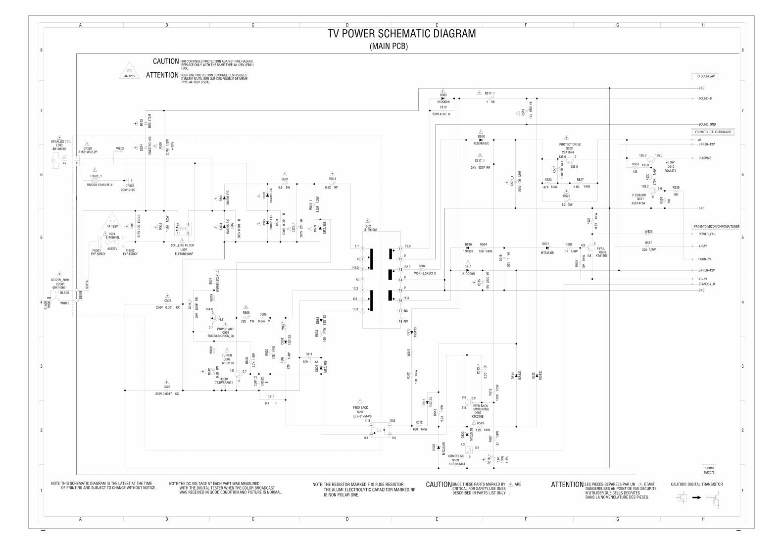
CAUTION: DIGITAL TRANSISTOR
S501
A
S501
B
IS NON POLAR ONE.THE ALUMI ELECTROLYTIC CAPACITOR MARKED NPTHE RESISTOR MARKED F IS FUSE RESISTOR.NOTE:
Q5102SA1371
+B SW
Q505KTA1266
P.FAIL
Q5032SA1624
PROTECT DRIVE
R501
5.6 5W
L501ELF15N010AP
COIL,LINE FILTER
1 2
3 4
21
L5038R140032
DEGAUSS COIL
FH502EYF-52BCY
FH501EYF-52BCY
F50151MS040L
4A125V
IC501LTV-817M-VB
FEED BACK
123
4
B504
W5RH3.5X5X1.0
B501
W5R
H3.5
X5X1
.0
TH501_1
B59203-S1060-B14
4A 125V
4A 125V
TYPE 4A 125V (F501).D’INCEIE N’UTILISER QUE DES FUSIBLE DE MEME
:POUR UNE PROTECTION CONTINUE LES RISQUESATTENTIONFUSE.REPLACE ONLY WITH THE SAME TYPE 4A 125V (F501)
CAUTION:FOR CONTINUED PROTECTION AGAINST FIRE HAZARD,
S
DG
Q5012SK3563(ORION_Q)
POWER AMP
BLACK
WHITE
BLAD
EW
IDE
CD50109414909
AC120V_60Hz
T50281291084
11
12
13
14
15
16
17
18
2
3
4
5
6
7
8
D524
ENE2
71D-
10A
D523
DSS-
272M
Q509KRC102MAT
COMPOUND
WAS RECEIVED IN GOOD CONDITION AND PICTURE IS NORMAL.WITH THE DIGITAL TESTER WHEN THE COLOR BROADCAST
NOTE:THE DC VOLTAGE AT EACH PART WAS MEASURED
C517_1
820P2KV RR
C513
_1
0.00
1CH
C514
_1
820P
2KV
RR
C518
470P500V B
C505
0.22
275V
ECQU
L
C503
0.00
150
0VB
C509
0.047 M
C508
0.0047250V KX
C502
0.00
150
0VB
C510
0.1 F
C501
_2
0.00
82B
C506
0.001250V KX
C507
1010
0VM
HE
C526
_1
220
200V
YK
C511
150V KA
R533
1M
R534
10K
R530
270K
1/4W
R523
47K 1/4W
R527
5.6K 1/4W R535
10K
R528
6.8K
1/4W
R513
2.2K
1/4W
R509
220
1/4W
R515
120K
1/2W
R512
680 1/4W
R504
100 1/4W
R505
1K 1/4W
R500
2.7M
1/2W
+-10
%
R516
10K
1/4W
R502
100
1/4W
R538
1.5M
1/2W
R506
2.7K
1/4W
R519
1.2K 1/4W
R507
271/
4W
R537
22K 1/2W
R510
_1
3.3M
1/2W
R503
100
1/4W
R520
12K
1/4W
OF PRINTING AND SUBJECT TO CHANGE WITHOUT NOTICENOTE:THIS SCHEMATIC DIAGRAM IS THE LATEST AT THE TIME
DANS LA NOMENCLATURE DES PIECESN’UTILISER QUE CELLS DECRITESDANGEREUSES AN POINT DE VUE SECURITE
:LES PIECES REPAREES PAR UN ETANTATTENTION:SINCE THESE PARTS MARKED BYCAUTIONDESCRIBED IN PARTS LIST ONLYCRITICAL FOR SAFETY,USE ONES
ARE
W83
0
W81
0
W82
7
W81
9
W802
W832D509
MTZ
J18B
D521
MTZJ5.6B
D520
MTZ
J5.1
B
D528
MTZ
J5.6
B
D506
MTZ
J10B
D514
1SS1
33
D522
1SS1
33
D511
1SS1
33
D508
1SS1
33
D505
21DQ09N
D501
1N40
05-E
IC
D502
1N40
05-E
IC
D503
1N40
05-E
IC
D516
1N4937
D513
21DQ09N
D515
1SS1
33
D504
1N40
05-E
IC
D510
RU2AM-EIC
D512
1SS1
33
Q5112SC1473A
P.CON SW
Q502KTC3198
BUFFER
Q507KTC3198
FEED BACKSWITCHING
R525
1.2 2W
R517_1
1 1W
R508
220 1W
R542
0.68
1W
GND
SOUND+B
SOUND_GND
+BUNREG+12V
P.CON+B
GND
POWER_FAIL
X-RAY
P.CON+5V
UNREG+12V
AT+5V
STANDBY_H
GND
10.0
144.0
NC10.3
6.6
10.3
PCB010TMC573
5.97.3
135.0
5.0135.0
0
135.0 135.0
TO SOUND/AV
FROM/TO DEFLECTION/CRT
FROM/TO MICON/CHROMA/TUNER
135.0
NC
NC
TV POWER SCHEMATIC DIAGRAM(MAIN PCB)
9.50.1
10.511.5
144.0
NC
0
0
1.7
0
132.3
11.3
9.5
5.5
6.0
0.1
0
4.8
0
135.0 0
0.1
4.8
4.9 0
4.8
A B C D E F G H
A B C D E F G H
2
1
3
4
5
6
7
8
2
1
3
4
5
6
7
8
TP024TP022 TP023
TP401
CP401A1561WV2-A5P
1
2
3
4
5
IC401 AN5522V-OUT IC
1 2 3 4 5 6 7
T401ETH09K14BZ
1
2
3 4
6
BGR
1168
109
175
V801A34AGT13X98_J(L)
F
J801ISMS01S
1
345
67
8 9
CD801_1
Q4012SC5885
H.OUTPUTVIDEO
8
E8E25
E12
GND
TERHEAAFC
B+
GND
ABL
GND
COLHV
F
S
FB401 FNI14B002_M
1
10
11
2
3
4
5
6
7
8
9
L801
220u
H
CD802
CD803 CP803B B2013H02-4P
1
2
3
4
CP803A B2013H02-4P
1
2
3
4
CP802AB2013H02-5P
1
2
3
4
5
CP802BB2013H02-5P
1
2
3
4
5
C427 10
50V
YKC417
4725
VYK
CP801131001101K1
1
HS401763WSAA021
HS402763WSAA019
R401_1
27K 1/4W +-1%
R408
_1
10K
1/4W
+-1%
R409_1
27K 1/4W +-1%
R429
4.7 1W
R404
681/
2W
CP806
IS NON POLAR ONE.THE ALUMI ELECTROLYTIC CAPACITOR MARKED NPTHE RESISTOR MARKED F IS FUSE RESISTOR.NOTE:
WAS RECEIVED IN GOOD CONDITION AND PICTURE IS NORMAL.WITH THE DIGITAL TESTER WHEN THE COLOR BROADCAST
NOTE:THE DC VOLTAGE AT EACH PART WAS MEASURED
C406
150P500V B
C420
_1
820P
2KV
RR
C410
_1
0.00
1CH
C422 0.
1510
0VM
KT
C437
0.47
250V
PMS
C440
0.01
100V
MM
TS
C819
_1
0.00
12K
VB
C810
_1
330P
CH
C809
_1
330P
CH
C808
_1
330P
CH
C423
220P CH
C443
0.00
861.
25KV
MPP
C448
_1
2225
0VYK
C414 10
035
V YK
C418
470
25V
YK
C403 47
035
V YK C435
0.1
100V
MHE
C446 22
50V
YK
C434
2210
0VYK
C401
125
0VM
HE
R806
2.7K
1/4W
R802
2.7K
1/4W
R804
_12.
7K1/
2W
R403
10K 1/4W
R448
560 1/2W
R449
560 1/2W
R416
11/
2W
R422
2.2
1/2W
R417
10K
1/4W
R815
330
1/4W
R813
330
1/4W
R420
2.7K
R421
220K
1/4W
R445
180K 1/4W
R410
330
1/2W
R415
1.8K 1/2W
R816
330
1/4W
R413
2.2K
1/2W
R419 47
0
R418
22K 1/4W
R446
470
1/2W
R423
100 1/4WR424
470 1/4W
R814
4.7K
1/4W
R811
4.7K
1/4W
R809
4.7K
1/4W
R427
100
1/4W
R405
1K1/
4W
OF PRINTING AND SUBJECT TO CHANGE WITHOUT NOTICENOTE:THIS SCHEMATIC DIAGRAM IS THE LATEST AT THE TIME
DANS LA NOMENCLATURE DES PIECESN’UTILISER QUE CELLS DECRITESDANGEREUSES AN POINT DE VUE SECURITE
:LES PIECES REPAREES PAR UN ETANTATTENTION
:SINCE THESE PARTS MARKED BYCAUTIONDESCRIBED IN PARTS LIST ONLYCRITICAL FOR SAFETY,USE ONES
ARE
W817
W831
W826
D404
MTZ
J6.2
B
D412
MTZ
J5.1
B
D413
MTZ
J5.6
B
DEFLECTION SIGNALB.SIGNAL
G.SIGNAL
R.SIGNAL
D409
11E1
-EIC
D403
11E1-EIC
D410
AU02
A-EI
C
D405
AU02
A-EI
C
D408
11E1
-EIC
D406
11E1-EIC
D411
AU02A-EIC
Q4022SC1627_Y
H.DRIVE
Q8012SC1473A
RED OUTQ802
2SC1473A
GREEN OUTQ803
2SC1473A
BLUE OUT
R803
_115
K1W
R805
_115
K1W
R807
_115
K1W
R447
150 2W
L401
4.7m
H
S803Y
GND GND
CLAMP CLAMP CLAMP
G.OUT G.OUT G.OUT
R.OUT R.OUT R.OUT
B.OUT B.OUT B.OUT
HEATER HEATER
GND GND
180V 180V
X-RAY
P.CON+B
GND
V_FEEDBACK
V_OUT
ABCL
H_OUT
H_SYNC
GND
+B
P.CON+B
UNREG+12V
48.0
132.5
132.5
130.0
0
25.0
1
NC NC
GND GND
CLAMP CLAMP
G.OUT G.OUT
R.OUT R.OUT
B.OUT B.OUT
HEATER
GND
NC
180V
HEATER
GND
NC
180V
FROM/TO TV POWER
FROM/TO MICON//CHROMA/TUNER
9
NC
NC
TO DY
SCREEN
FOCUS
NC
FOCUS
SCREEN
130.0
00
0
27.0
0.3
3.2
2.7
100.6
3.2
2.7
98.4
3.2
2.7
95.4
3.5 2.0 12.0 25.0 3.5
0
025.0
4.3
(MAIN PCB)DEFLECTION/CRT SCHEMATIC DIAGRAM
NC
00
0
101.6
6.4 99.6
96.4
AMP
THERMALPROTECTION
PUMPUP
PCB010TMC573
PCB110TCC434
FROM MICON/CHROMA/TUNER
14 15 16
13
12
8
10
11
7.0
0
A B C D E F G H
A B C D E F G H
2
1
3
4
5
6
7
8
2
1
3
4
5
6
7
8
AUDIO SIGNAL
SPEAKER
SP1001YDP47-58
8 OHM
J1001MSJ-035-12A_PC
EAR PHONE_JACK
1
2
3
H E
J703AV1-09AD-4
RCA JACK WHITE
12H E
J702AV1-09AD-3
RCA JACK YELLOW
12 ANT001HPAS-2S400
TM101EUR7713020
BT001R6SPTT
UM-4
BT002R6SPTT
UM-4
C1006
4716V KANP
C100
3
150
VKA
CD101BCH013203
CD101ACH013202
WAS RECEIVED IN GOOD CONDITION AND PICTURE IS NORMAL.WITH THE DIGITAL TESTER WHEN THE COLOR BROADCAST
NOTE:THE DC VOLTAGE AT EACH PART WAS MEASURED
C100
4_2
0.00
27B
C1001
0.150V KA
C100
7
1000
10V
YK
C100
5
1025
VKA
R703
820
R1003
68KR1
005
270K
R100
4
100K
R1001
47K 1/4W
R100
8
39K
R701
681/
4W
R704
10 1/2W
R1007
47 1/2W
R702
47K
OF PRINTING AND SUBJECT TO CHANGE WITHOUT NOTICENOTE:THIS SCHEMATIC DIAGRAM IS THE LATEST AT THE TIME
DANS LA NOMENCLATURE DES PIECESN’UTILISER QUE CELLS DECRITESDANGEREUSES AN POINT DE VUE SECURITE
:LES PIECES REPAREES PAR UN ETANTATTENTION:SINCE THESE PARTS MARKED BYCAUTIONDESCRIBED IN PARTS LIST ONLYCRITICAL FOR SAFETY,USE ONES
ARE
W81
3
W811
W80
3
IC10
01AN
7511
SOUN
D AM
P IC
1234
5 6 7 8
TUNER VIDEO SIGNALD7
03
MTZ
J12B
D701
MTZ
J6.8
B
D704
MTZ
J9.1
B
D702
MTZ
J5.6
B
D705
MTZ
J9.1
B
AUDIO_IN
VIDEO_IN
GND
SOUND_GND
SOUND+B
GND
AUDIO_MUTE
P.CON+5V
GND
AUDIO_OUTPCB010TMC573
11
22
FROM MICON/CHROMA/TUNER
FROM TV POWER
TO MICON/CHROMA/TUNER
18
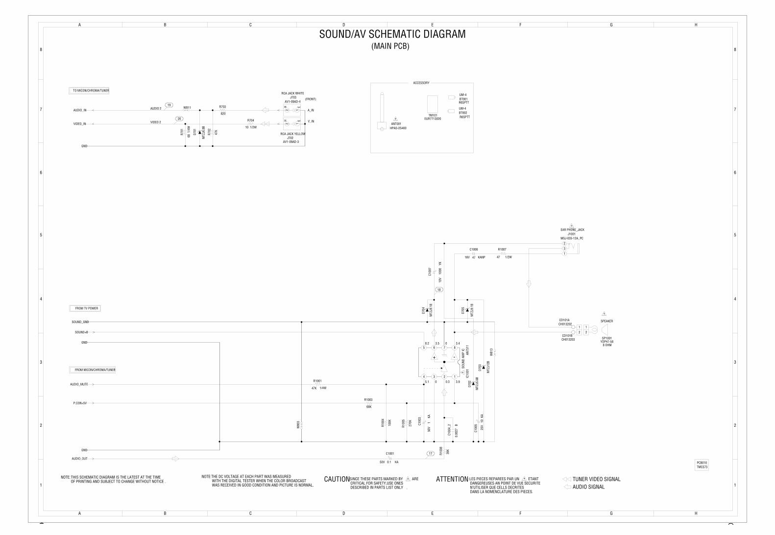
VIDEO 2
AUDIO 2
(FRONT)
V_IN
A_IN
-+
0
08.2 3.5 3.4
3.95.1 0.3
SOUND/AV SCHEMATIC DIAGRAM(MAIN PCB)
ACCESSORY
19
20
17
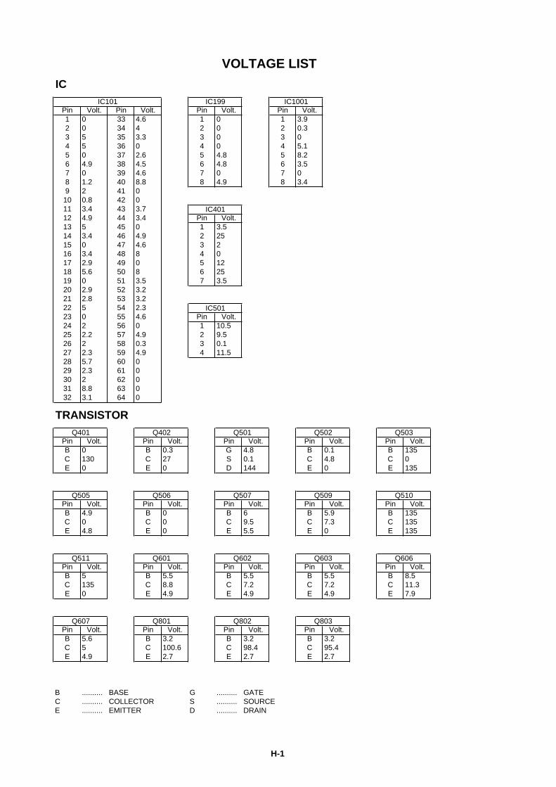
IC
Pin Volt. Pin Volt. Pin Volt. Pin Volt.1 0 33 4.6 1 0 1 3.92 0 34 4 2 0 2 0.33 5 35 3.3 3 0 3 04 5 36 0 4 0 4 5.15 0 37 2.6 5 4.8 5 8.26 4.9 38 4.5 6 4.8 6 3.57 0 39 4.6 7 0 7 08 1.2 40 8.8 8 4.9 8 3.49 2 41 010 0.8 42 011 3.4 43 3.712 4.9 44 3.4 Pin Volt.13 5 45 0 1 3.514 3.4 46 4.9 2 2515 0 47 4.6 3 216 3.4 48 8 4 017 2.9 49 0 5 1218 5.6 50 8 6 2519 0 51 3.5 7 3.520 2.9 52 3.221 2.8 53 3.222 5 54 2.323 0 55 4.6 Pin Volt.24 2 56 0 1 10.525 2.2 57 4.9 2 9.526 2 58 0.3 3 0.127 2.3 59 4.9 4 11.528 5.7 60 029 2.3 61 030 2 62 031 8.8 63 032 3.1 64 0
TRANSISTOR
Pin Volt. Pin Volt. Pin Volt. Pin Volt. Pin Volt.B 0 B 0.3 G 4.8 B 0.1 B 135C 130 C 27 S 0.1 C 4.8 C 0E 0 E 0 D 144 E 0 E 135
Pin Volt. Pin Volt. Pin Volt. Pin Volt. Pin Volt.B 4.9 B 0 B 6 B 5.9 B 135C 0 C 0 C 9.5 C 7.3 C 135E 4.8 E 0 E 5.5 E 0 E 135
Pin Volt. Pin Volt. Pin Volt. Pin Volt. Pin Volt.B 5 B 5.5 B 5.5 B 5.5 B 8.5C 135 C 8.8 C 7.2 C 7.2 C 11.3E 0 E 4.9 E 4.9 E 4.9 E 7.9
Pin Volt. Pin Volt. Pin Volt. Pin Volt.B 5.6 B 3.2 B 3.2 B 3.2C 5 C 100.6 C 98.4 C 95.4E 4.9 E 2.7 E 2.7 E 2.7
B .......... BASE G .......... GATEC .......... COLLECTOR S .......... SOURCEE .......... EMITTER D .......... DRAIN
Q607
Q502
Q603
Q802Q801
Q606Q602
Q803
IC101 IC199
VOLTAGE LIST
Q503Q401 Q402 Q501
IC401
IC1001
IC501
Q505 Q510
Q511 Q601
Q506 Q507 Q509
H-1
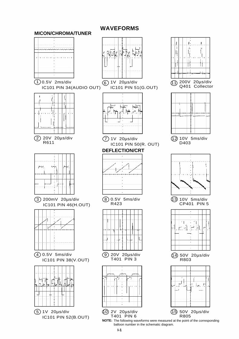
WAVEFORMS
1V 20µs/divIC101 PIN 52(B.OUT)
MICON/CHROMA/TUNER
1 0.5V 2ms/divIC101 PIN 34(AUDIO OUT)
NOTE: The following waveforms were measured at the point of the correspondingballoon number in the schematic diagram.
2 20V 20µs/divR611
3 200mV 20µs/divIC101 PIN 46(H.OUT)
0.5V 5ms/divIC101 PIN 38(V.OUT)
4
5
6 1V 20µs/divIC101 PIN 51(G.OUT)
DEFLECTION/CRT
0.5V 5ms/divR423
1V 20µs/divIC101 PIN 50(R. OUT)
7
8
9 20V 20µs/divT401 PIN 3
10 2V 20µs/divT401 PIN 6
200V 20µs/divQ401 Collector
11
10V 5ms/divD403
12
10V 5ms/divCP401 PIN 5
13
50V 20µs/divR803
14
15 50V 20µs/divR805
I-1

WAVEFORMS
NOTE: The following waveforms were measured at the point of the correspondingballoon number in the schematic diagram.
16 50V 20µs/divR807
SOUND/AV
0.5V 1ms/divC1001
17
1V 1ms/divIC1001 PIN 6
18
200mV 500µs/divR703
19
20 500mV 20µs/divR704
I-2
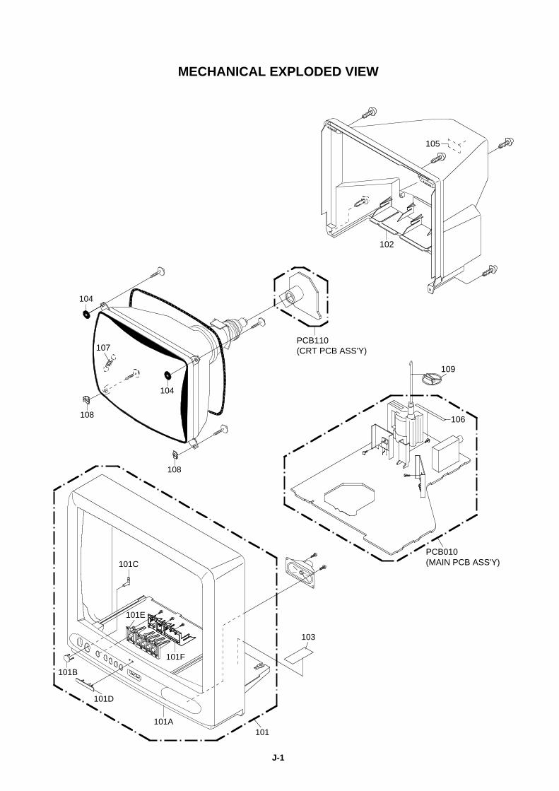
MECHANICAL EXPLODED VIEW
J-1
102
105
PCB110(CRT PCB ASS'Y)
104
104
108
108
107
PCB010(MAIN PCB ASS'Y)
106
109
101A
101D
101B
103
101
101E
101F
101C

MECHANICAL REPLACEMENT PARTS LIST
Location No. Part No. Description Reference No. 101 7A701A384A FRONT CABI ASS'Y 101A 701WPJD014 CABINET,FRONT 101B 711WPAA125 PLATE,FRONT 101C 713WPAA193 GUIDE,REMOCON 101D 723576A004 BADGE,BRAND 101E 735WPAA958 BUTTONN,FRAME 101F 735WPAA959 BUTTON,BASE
102 702WPAA857 CABINET,BACK
103 723000C727 SHEET,CAUTION 104 800WR0A011 SHEET,CRT SUPPORT (D) 105 726000A091 SHEET,CRT SERVICEMAN 106 800WQ0A064 FELT SHEET 107 741WUA0021 SPRING,EARTH 108 769WSAA011 WASHER CRT T=1 109 899HV3T000 HOLDER,ANODE WIRE
--- J3M13301A INSTRUCTION BOOK
K1-1
ELECTRICAL REPLACEMENT PARTS LIST
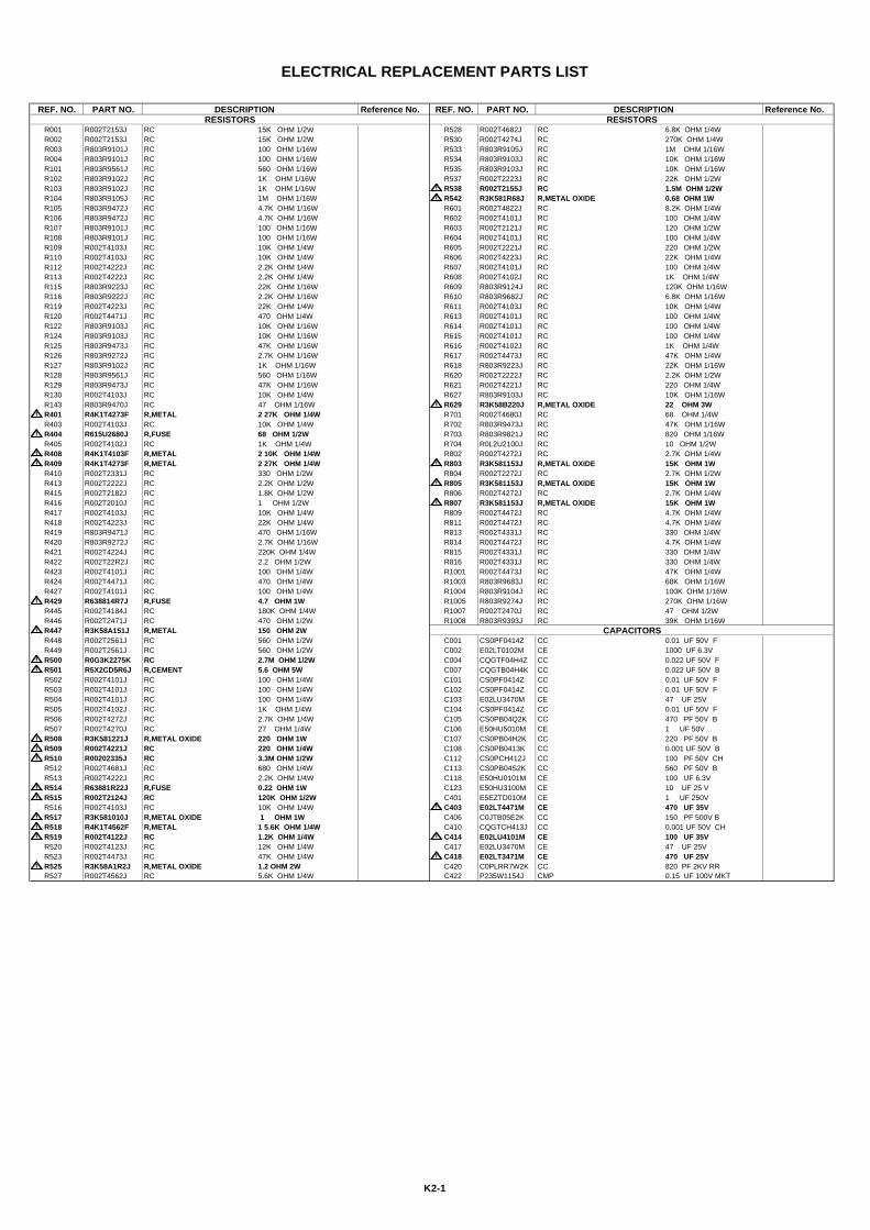
REF. NO. PART NO. DESCRIPTION Reference No. REF. NO. PART NO. DESCRIPTION Reference No.RESISTORS RESISTORS
R001 R002T2153J RC 15K OHM 1/2W R528 R002T4682J RC 6.8K OHM 1/4W R002 R002T2153J RC 15K OHM 1/2W R530 R002T4274J RC 270K OHM 1/4W R003 R803R9101J RC 100 OHM 1/16W R533 R803R9105J RC 1M OHM 1/16W R004 R803R9101J RC 100 OHM 1/16W R534 R803R9103J RC 10K OHM 1/16W R101 R803R9561J RC 560 OHM 1/16W R535 R803R9103J RC 10K OHM 1/16W R102 R803R9102J RC 1K OHM 1/16W R537 R002T2223J RC 22K OHM 1/2W R103 R803R9102J RC 1K OHM 1/16W ! R538 R002T2155J RC 1.5M OHM 1/2W R104 R803R9105J RC 1M OHM 1/16W ! R542 R3K581R68J R,METAL OXIDE 0.68 OHM 1W R105 R803R9472J RC 4.7K OHM 1/16W R601 R002T4822J RC 8.2K OHM 1/4W R106 R803R9472J RC 4.7K OHM 1/16W R602 R002T4101J RC 100 OHM 1/4W R107 R803R9101J RC 100 OHM 1/16W R603 R002T2121J RC 120 OHM 1/2W R108 R803R9101J RC 100 OHM 1/16W R604 R002T4101J RC 100 OHM 1/4W R109 R002T4103J RC 10K OHM 1/4W R605 R002T2221J RC 220 OHM 1/2W R110 R002T4103J RC 10K OHM 1/4W R606 R002T4223J RC 22K OHM 1/4W R112 R002T4222J RC 2.2K OHM 1/4W R607 R002T4101J RC 100 OHM 1/4W R113 R002T4222J RC 2.2K OHM 1/4W R608 R002T4102J RC 1K OHM 1/4W R115 R803R9223J RC 22K OHM 1/16W R609 R803R9124J RC 120K OHM 1/16W R116 R803R9222J RC 2.2K OHM 1/16W R610 R803R9682J RC 6.8K OHM 1/16W R119 R002T4223J RC 22K OHM 1/4W R611 R002T4103J RC 10K OHM 1/4W R120 R002T4471J RC 470 OHM 1/4W R613 R002T4101J RC 100 OHM 1/4W R122 R803R9103J RC 10K OHM 1/16W R614 R002T4101J RC 100 OHM 1/4W R124 R803R9103J RC 10K OHM 1/16W R615 R002T4101J RC 100 OHM 1/4W R125 R803R9473J RC 47K OHM 1/16W R616 R002T4102J RC 1K OHM 1/4W R126 R803R9272J RC 2.7K OHM 1/16W R617 R002T4473J RC 47K OHM 1/4W R127 R803R9102J RC 1K OHM 1/16W R618 R803R9223J RC 22K OHM 1/16W R128 R803R9561J RC 560 OHM 1/16W R620 R002T2222J RC 2.2K OHM 1/2W R129 R803R9473J RC 47K OHM 1/16W R621 R002T4221J RC 220 OHM 1/4W R130 R002T4103J RC 10K OHM 1/4W R627 R803R9103J RC 10K OHM 1/16W R143 R803R9470J RC 47 OHM 1/16W ! R629 R3K58B220J R,METAL OXIDE 22 OHM 3W ! R401 R4K1T4273F R,METAL 2 27K OHM 1/4W R701 R002T4680J RC 68 OHM 1/4W R403 R002T4103J RC 10K OHM 1/4W R702 R803R9473J RC 47K OHM 1/16W ! R404 R615U2680J R,FUSE 68 OHM 1/2W R703 R803R9821J RC 820 OHM 1/16W R405 R002T4102J RC 1K OHM 1/4W R704 R0L2U2100J RC 10 OHM 1/2W ! R408 R4K1T4103F R,METAL 2 10K OHM 1/4W R802 R002T4272J RC 2.7K OHM 1/4W ! R409 R4K1T4273F R,METAL 2 27K OHM 1/4W ! R803 R3K581153J R,METAL OXIDE 15K OHM 1W R410 R002T2331J RC 330 OHM 1/2W R804 R002T2272J RC 2.7K OHM 1/2W R413 R002T2222J RC 2.2K OHM 1/2W ! R805 R3K581153J R,METAL OXIDE 15K OHM 1W R415 R002T2182J RC 1.8K OHM 1/2W R806 R002T4272J RC 2.7K OHM 1/4W R416 R002T2010J RC 1 OHM 1/2W ! R807 R3K581153J R,METAL OXIDE 15K OHM 1W R417 R002T4103J RC 10K OHM 1/4W R809 R002T4472J RC 4.7K OHM 1/4W R418 R002T4223J RC 22K OHM 1/4W R811 R002T4472J RC 4.7K OHM 1/4W R419 R803R9471J RC 470 OHM 1/16W R813 R002T4331J RC 330 OHM 1/4W R420 R803R9272J RC 2.7K OHM 1/16W R814 R002T4472J RC 4.7K OHM 1/4W R421 R002T4224J RC 220K OHM 1/4W R815 R002T4331J RC 330 OHM 1/4W R422 R002T22R2J RC 2.2 OHM 1/2W R816 R002T4331J RC 330 OHM 1/4W R423 R002T4101J RC 100 OHM 1/4W R1001 R002T4473J RC 47K OHM 1/4W R424 R002T4471J RC 470 OHM 1/4W R1003 R803R9683J RC 68K OHM 1/16W R427 R002T4101J RC 100 OHM 1/4W R1004 R803R9104J RC 100K OHM 1/16W ! R429 R638814R7J R,FUSE 4.7 OHM 1W R1005 R803R9274J RC 270K OHM 1/16W R445 R002T4184J RC 180K OHM 1/4W R1007 R002T2470J RC 47 OHM 1/2W R446 R002T2471J RC 470 OHM 1/2W R1008 R803R9393J RC 39K OHM 1/16W ! R447 R3K58A151J R,METAL 150 OHM 2W CAPACITORS R448 R002T2561J RC 560 OHM 1/2W C001 CS0PF0414Z CC 0.01 UF 50V F R449 R002T2561J RC 560 OHM 1/2W C002 E02LT0102M CE 1000 UF 6.3V ! R500 R0G3K2275K RC 2.7M OHM 1/2W C004 CQGTF04H4Z CC 0.022 UF 50V F ! R501 R5X2CD5R6J R,CEMENT 5.6 OHM 5W C007 CQGTB04H4K CC 0.022 UF 50V B R502 R002T4101J RC 100 OHM 1/4W C101 CS0PF0414Z CC 0.01 UF 50V F R503 R002T4101J RC 100 OHM 1/4W C102 CS0PF0414Z CC 0.01 UF 50V F R504 R002T4101J RC 100 OHM 1/4W C103 E02LU3470M CE 47 UF 25V R505 R002T4102J RC 1K OHM 1/4W C104 CS0PF0414Z CC 0.01 UF 50V F R506 R002T4272J RC 2.7K OHM 1/4W C105 CS0PB04Q2K CC 470 PF 50V B R507 R002T4270J RC 27 OHM 1/4W C106 E50HU5010M CE 1 UF 50V ! R508 R3K581221J R,METAL OXIDE 220 OHM 1W C107 CS0PB04H2K CC 220 PF 50V B ! R509 R002T4221J RC 220 OHM 1/4W C108 CS0PB0413K CC 0.001 UF 50V B ! R510 R00202335J RC 3.3M OHM 1/2W C112 CS0PCH412J CC 100 PF 50V CH R512 R002T4681J RC 680 OHM 1/4W C113 CS0PB04S2K CC 560 PF 50V B R513 R002T4222J RC 2.2K OHM 1/4W C118 E50HU0101M CE 100 UF 6.3V ! R514 R63881R22J R,FUSE 0.22 OHM 1W C123 E50HU3100M CE 10 UF 25 V ! R515 R002T2124J RC 120K OHM 1/2W C401 E5EZTD010M CE 1 UF 250V R516 R002T4103J RC 10K OHM 1/4W ! C403 E02LT4471M CE 470 UF 35V ! R517 R3K581010J R,METAL OXIDE 1 OHM 1W C406 C0JTB05E2K CC 150 PF 500V B ! R518 R4K1T4562F R,METAL 1 5.6K OHM 1/4W C410 CQGTCH413J CC 0.001 UF 50V CH ! R519 R002T4122J RC 1.2K OHM 1/4W ! C414 E02LU4101M CE 100 UF 35V R520 R002T4123J RC 12K OHM 1/4W C417 E02LU3470M CE 47 UF 25V R523 R002T4473J RC 47K OHM 1/4W ! C418 E02LT3471M CE 470 UF 25V ! R525 R3K58A1R2J R,METAL OXIDE 1.2 OHM 2W C420 C0PLRR7W2K CC 820 PF 2KV RR R527 R002T4562J RC 5.6K OHM 1/4W C422 P235W1154J CMP 0.15 UF 100V MKT
K2-1
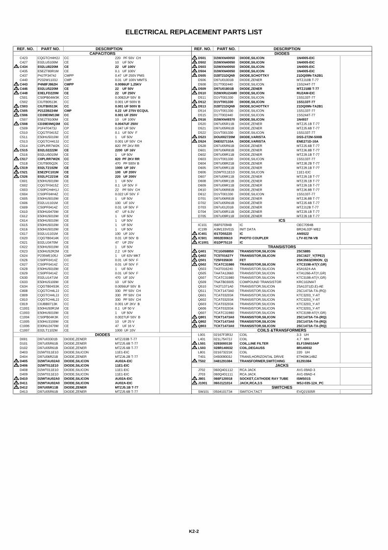
ELECTRICAL REPLACEMENT PARTS LIST
REF. NO. PART NO. DESCRIPTION REF. NO. PART NO. DESCRIPTIONCAPACITORS DIODES
C423 CQGTCH4H2J CC 220 PF 50V CH ! D501 D2WXN40050 DIODE,SILICON 1N4005-EIC C427 E02LU5100M CE 10 UF 50V ! D502 D2WXN40050 DIODE,SILICON 1N4005-EIC ! C434 E02LU8220M CE 22 UF 100V ! D503 D2WXN40050 DIODE,SILICON 1N4005-EIC C435 E5EZT80R1M CE 0.1 UF 100V ! D504 D2WXN40050 DIODE,SILICON 1N4005-EIC C437 P4J7F3474J CMPP 0.47 UF 250V PMS ! D505 D28T21DQN9 DIODE,SCHOTTKY 21DQ09N-TA2B1 C440 P232W1103J CMP 0.01 UF 100V MMTS D506 D97U01001B DIODE,ZENER MTZJ10B T-77 ! C443 P4N8FJ862H CMPP 0.0086UF 1.25KV D508 D17T002440 DIODE,SILICON 1SS244T-77 ! C446 E02LU5220M CE 22 UF 50V ! D509 D97U01801B DIODE,ZENER MTZJ18B T-77 ! C448 E0ELFD220M CE 22 UF 250V ! D510 D2WXRU2AM0 DIODE,SILICON RU2AM-EIC C501 CS0PB04W3K CC 0.0082UF 50V B D511 D1VT001330 DIODE,SILICON 1SS133T-77 C502 C0JTB0513K CC 0.001 UF 500V B ! D512 D1VT001330 DIODE,SILICON 1SS133T-77 ! C503 C0JTB0513K CC 0.001 UF 500V B ! D513 D28T21DQN9 DIODE,SCHOTTKY 21DQ09N-TA2B1 ! C505 P2122B224M CMP 0.22 UF 275V ECQUL D514 D1VT001330 DIODE,SILICON 1SS133T-77 ! C506 CD39E0M13M CC 0.001 UF 250V D515 D17T002440 DIODE,SILICON 1SS244T-77 C507 E5EZT8100M CE 10 UF 100V ! D516 D2WXN49370 DIODE,SILICON 1N4937 ! C508 CD39E0MQ3M CC 0.0047UF 250V D520 D97U05R11B DIODE,ZENER MTZJ5.1B T-77 C509 P1F4T0473J CP 0.047 UF 50V D521 D97U05R61B DIODE,ZENER MTZJ5.6B T-77 C510 CQGTF0415Z CC 0.1 UF 50V F D522 D1VT001330 DIODE,SILICON 1SS133T-77 C511 E50HU5010M CE 1 UF 50V ! D523 DOU002720M DIODE,VARISTA DSS-272M-S00B C513 CQGTCH413J CC 0.001 UF 50V CH ! D524 D6E027110A DIODE,VARISTA ENE271D-10A C514 C0PLRR7W2K CC 820 PF 2KV RR D528 D97U05R61B DIODE,ZENER MTZJ5.6B T-77 ! C515 E02L02222M CE 2200 UF 16V D601 D97U06R81B DIODE,ZENER MTZJ6.8B T-77 C516 E02LU5010M CE 1 UF 50V D602 D97U09R11B DIODE,ZENER MTZJ9.1B T-77 ! C517 C0PLRR7W2K CC 820 PF 2KV RR D603 D1VT001330 DIODE,SILICON 1SS133T-77 C518 C0JTB05Q2K CC 470 PF 500V B D604 D97U08R21B DIODE,ZENER MTZJ8.2B T-77 ! C519 E02LT2102M CE 1000 UF 16V D605 D97U09R11B DIODE,ZENER MTZJ9.1B T-77 ! C521 E5EZFC101M CE 100 UF 200V D606 D2WT011E10 DIODE,SILICON 11E1-EIC ! C526 E02LFC221M CE 220 UF 200V D607 D97U09R11B DIODE,ZENER MTZJ9.1B T-77 C601 E50HU5010M CE 1 UF 50V D608 D97U09R11B DIODE,ZENER MTZJ9.1B T-77 C602 CQGTF0415Z CC 0.1 UF 50V F D609 D97U09R11B DIODE,ZENER MTZJ9.1B T-77 C603 CS0PCH4H1J CC 22 PF 50V CH D610 D97U06R81B DIODE,ZENER MTZJ6.8B T-77 C604 CS0PF04H4Z CC 0.022 UF 50V F D612 D1VT001330 DIODE,SILICON 1SS133T-77 C605 E50HU5010M CE 1 UF 50V D701 D97U06R81B DIODE,ZENER MTZJ6.8B T-77 C606 E02LU1101M CE 100 UF 10V D702 D97U05R61B DIODE,ZENER MTZJ5.6B T-77 C609 CS0PF0414Z CC 0.01 UF 50V F D703 D97U01201B DIODE,ZENER MTZJ12B T-77 C610 E50HU0470M CE 47 UF 6.3V D704 D97U09R11B DIODE,ZENER MTZJ9.1B T-77 C612 E50HU5010M CE 1 UF 50V D705 D97U09R11B DIODE,ZENER MTZJ9.1B T-77 C614 E50HU5010M CE 1 UF 50V ICS C615 E50HU5010M CE 1 UF 50V IC101 I56F07094B IC OEC7094B C616 E50HU5010M CE 1 UF 50V IC199 A3M133V015 INIT DATA BR24L02F-WE2 C617 E02LU1101M CE 100 UF 10V ! IC401 I01TD55220 IC AN5522 C620 CQGTB0414K CC 0.01 UF 50V B ! IC501 0002E00610 PHOTO COUPLER LTV-817M-VB C621 E02LU3470M CE 47 UF 25V ! IC1001 I01DP75110 IC C622 E50HU5010M CE 1 UF 50V TRANSISTORS C623 E50HU52R2M CE 2.2 UF 50V ! Q401 TC1G058850 TRANSISTOR,SILICON 2SC5885 C624 P235WE105J CMP 1 UF 63V MKT ! Q402 TC5T01627Y TRANSISTOR,SILICON 2SC1627_Y(TPE2) C626 CS0PF0414Z CC 0.01 UF 50V F ! Q501 T25F035630 FET 2SK3563(ORION_Q) C627 CS0PF0414Z CC 0.01 UF 50V F ! Q502 TCATC31980 TRANSISTOR,SILICON KTC3198-AT(Y,GR) C628 E50HU5010M CE 1 UF 50V Q503 TA3T016240 TRANSISTOR,SILICON 2SA1624-AA C629 CS0PF0414Z CC 0.01 UF 50V F Q505 TAATA12660 TRANSISTOR,SILICON KTA1266-AT(Y,GR) C630 E02LU1471M CE 470 UF 10V Q507 TCATC31980 TRANSISTOR,SILICON KTC3198-AT(Y,GR) C633 E50HU5100M CE 10 UF 50V Q509 TNATB03005 COMPOUND TRANSISTOR KRC102MAT C634 CQGTB04S3K CC 0.0056UF 50V B Q510 TA3T1371A0 TRANSISTOR,SILICON 2SA1371(D,E)-AE C808 CQGTCH4L2J CC 330 PF 50V CH Q511 TCKT1473A0 TRANSISTOR,SILICON 2SC1473A-TA-(RQ) C809 CQGTCH4L2J CC 330 PF 50V CH Q601 TCAT032034 TRANSISTOR,SILICON KTC3203_Y-AT C810 CQGTCH4L2J CC 330 PF 50V CH Q602 TCAT032034 TRANSISTOR,SILICON KTC3203_Y-AT C819 C0JBB0713K CC 0.001 UF 2KV B Q603 TCAT032034 TRANSISTOR,SILICON KTC3203_Y-AT C1001 E50HU50R1M CE 0.1 UF 50 V Q606 TCAT032034 TRANSISTOR,SILICON KTC3203_Y-AT C1003 E50HU5010M CE 1 UF 50V Q607 TCATC31980 TRANSISTOR,SILICON KTC3198-AT(Y,GR) C1004 CS0PB04K3K CC 0.0027UF 50V B ! Q801 TCKT1473A0 TRANSISTOR,SILICON 2SC1473A-TA-(RQ) C1005 E50HU3100M CE 10 UF 25 V ! Q802 TCKT1473A0 TRANSISTOR,SILICON 2SC1473A-TA-(RQ) C1006 E00NU2470M CE 47 UF 16 V ! Q803 TCKT1473A0 TRANSISTOR,SILICON 2SC1473A-TA-(RQ) C1007 E02LT1102M CE 1000 UF 10V COILS &TRANSFORMERS
DIODES L001 02167F3R3J COIL 3.3 UH D001 D97U03301B DIODE,ZENER MTZJ33B T-77 L401 021L75472J COIL 4.7 MH D101 D97U05R61B DIODE,ZENER MTZJ5.6B T-77 ! L501 0293000130 COIL,LINE FILTER ELF15N010AP D102 D97U05R61B DIODE,ZENER MTZJ5.6B T-77 ! L503 028R140032 COIL,DEGAUSS 8R140032 D403 D2WT011E10 DIODE,SILICON 11E1-EIC L801 021673221K COIL 220 UH D404 D97U06R21B DIODE,ZENER MTZJ6.2B T-77 T401 045009003J TRANS,HORIZONTAL DRIVE ETH09K14BZ ! D405 D2WTAU02A0 DIODE,SILICON AU02A-EIC ! T502 0481291084 TRANSFORMER,SWITCHING 81291084 ! D406 D2WT011E10 DIODE,SILICON 11E1-EIC JACKS D408 D2WT011E10 DIODE,SILICON 11E1-EIC J702 060Q401112 RCA JACK AV1-09AD-3 D409 D2WT011E10 DIODE,SILICON 11E1-EIC J703 060Q401111 RCA JACK AV1-09AD-4 ! D410 D2WTAU02A0 DIODE,SILICON AU02A-EIC ! J801 066F120018 SOCKET,CATHODE RAY TUBE ISMS01S ! D411 D2WTAU02A0 DIODE,SILICON AU02A-EIC ! J1001 060J121014 JACK,RCA,3.5 MSJ-035-12A_PC ! D412 D97U05R11B DIODE,ZENER MTZJ5.1B T-77 SWITCHES D413 D97U05R61B DIODE,ZENER MTZJ5.6B T-77 SW101 0504101T34 SWITCH,TACT EVQ21505R
K2-2

ELECTRICAL REPLACEMENT PARTS LIST
REF. NO. PART NO. DESCRIPTIONSWITCHES
SW102 0504101T34 SWITCH,TACT EVQ21505R SW103 0504101T34 SWITCH,TACT EVQ21505R SW104 0504101T34 SWITCH,TACT EVQ21505R SW105 0504101T34 SWITCH,TACT EVQ21505R
P.C.BOARD ASSEMBLIES PCB010 A3M133V010 PCB ASS'Y TMC573C PCB110 A3M133V110 PCB ASS'Y TCC434C
MISCELLANEOUS ! ANT001 125C104001 ANTENNA,ROD HPAS-2S400 B501 024HT03553 CORE,BEADS W5RH3.5X5X1.0 B504 024HT03553 CORE,BEADS W5RH3.5X5X1.0 ! CD501 1209414909 CORD,AC BUSH 9414909 ! CP401 069S450089 CONNECTOR PCB SIDE A1561WV2-A5P ! CP502 069S420110 CONNECTOR PCB SIDE A1561WV2-2P CP503 069W01001A CONNECTOR PCB SIDE CP601 069S260639 CONNECTOR PCB SIDE A2001WR2-6P CP801 069W010340 CONNECTOR PCB SIDE 131001101K1 CD101A 06CH013202 CORD,CONNECTOR CH013202 CD101B 06CH013203 CORD,CONNECTOR CH013203 ! F501 081PC04005 FUSE 51MS040L ! FB401 043214050F TRANSFORMER,FLYBACK FNI14B002_M OS101 0773071005 REMOTE RECEIVER RPM7137-WH5 S101 WBL6026038 FLAT CABLE AWM2468 A WG26 4C BLACK 260MM S102 WCL6834038 FLAT CABLE AWM2468 A WG26 5C GRAY 340MM ! SP1001 070N533034 SPEAKER YDP47-58 ! TH501 D8EE0B1400 DEGAUSS ELEMENT B59203-S1060-B14 TM101 076G0GP010 TRANSMITTER EUR7713020 ! TU001 0163100017 RF UNIT ENG36A29GF ! V801 098Q1404B3 CRT W/DY A34AGT13X98_J(L) X601 100CT3R505 CRYSTAL HC-49/U
RESISTORRC................... CARBON RESISTOR
CAPACITORSCC................... CERAMIC CAPACITORCE................... ALUMI ELECTROLYTIC CAPACITORCP................... POLYESTER CAPACITORCPP.................. POLYPROPYLENE CAPACITORCPL.................. PLASTIC CAPACITORCMP.................... METAL POLYESTER CAPACITORCMPL................ METAL PLASTIC CAPACITORCMPP................ METAL POLYPROPYLENE CAPACITOR
K2-3

Printed in U.S.A.