Embed Size (px)
Citation preview
Energies 2010, 3
314
includes devices with flat and bulk heterojunction between the various types of conjugated polymers,
small molecules, fullerene derivatives, and carbon nanotubes [1-3]. Despite substantial progress in
solar cell architecture, design and rational choice of the donor-acceptor materials over the past two
decades, organic PVs are still unable to overcome the 6–7% barrier of conversion efficiency [4,5]. In
terms of the low conversion efficiency, there are currently at least four major fundamental aspects
making organic PVs vulnerable for commercial applications as compared with conventional
semiconducting solar cells: (i) low carrier mobility, (ii) lack of absorption in the red/NIR part of
spectrum, (iii) poor environmental stability, and (iv) excitonic character of photocarrier generation. If
the first three above-mentioned statements are obvious, the fourth requires some explanation.
The source of photocarriers in organics is small radius excitons generated as a result of photon
absorption. Excitons in organics have a binding energy in the range 200–400 meV [6,7], which is
considerably higher than the binding exciton energy for semiconductor materials ~2–40 meV [8].
Thermal energy at room temperature is not sufficient (~25 meV) for exciton dissociation to hole and
electron in the bulk medium. Therefore, exciton dissociation should occur at the interface between the
donor and acceptor materials with proper HOMO and LUMO energy levels. The mechanism of
exciton dissociation is not completely understood, however the major factor governing the charge
separation at the interface is the charge transfer process between the donor and acceptor components.
After charge separation, holes and electrons move to the opposite electrodes owing to drift (induced by
the electric field at the interface) and diffusion (gradient of the charge concentration from the interface
to the surface). In the case of a flat heterojunction, the diffusion length of the singlet excitons (several
tens nanometers) should be comparable with the thickness of at least of one active layer (donor or
acceptor) to minimize energy loss, otherwise not all excitons are able to reach the interface. However,
at such small thickness, the absorbed energy is very low since the penetration length of incident light
for organics is typically more than 100 nm. The possible solution could be formation of bulk
heterojunctions (blend of donor and acceptor materials) with separation scale factor comparable with
the excitonic diffusion lengths and relatively thick films to absorb more light energy. Nevertheless, an
increase of the film thickness should result in a longer photocarrier pathway to the external electrodes,
which reduces the conversion efficiency owing to carriers trapping and lower carrier mobility.
An alternative to pure organic PVs is the class of organic-inorganic hybrid solar cells [9-12], where
heterojunction is formed between inorganic semiconductors and organic compounds (small molecules,
oligomers, polymers, carbon nanotubes). An advantage of hybrid PVs over organics PVs lies in the
high carrier mobility of the semiconductor and the light absorption at longer wavelengths than for
organic compounds. On the other hand, the existence of the organic component allows hybrid solar
cells to be superior over conventional semiconducting PVs in terms of cost efficiency, scalable wet
processing, the variety of organic materials (mismatch between inorganic components can be
minimized or prevented), light weight, and flexibility. Moreover, the recent progress in advanced
semiconducting nanostructures in combination with organic nanomaterials [e.g., fullerenes and carbon
nanotubes (CNTs)] opens new opportunities to overcome the 10% barrier of conversion efficiency for
hybrid solar cells in the near future. Note, that band engineering can be a useful instrument in the
design of the hybrid solar cell architecture, however it is not as straightforward as for semiconducting
PVs. For example, the chemical functionalizing of the organic component (introduction of reducing or
oxidizing groups in the chemical structure) is capable of significantly affecting the band gap energy
Energies 2010, 3
315
and position of the Fermi level for conducting polymers and small molecules. Even physical doping
(e.g., by simple exposure of polymer film upon iodine vapors) can strongly increase the polymer
conductivity and reduce its transparency, thus altering the polymer optoelectronic properties. Thus, the
PV performance of hybrid solar cell can be readily optimized by tuning the band structure of organic
component (work function, band gap, Fermi level) for the best matching with the corresponding band
structure of the inorganic counterpart.
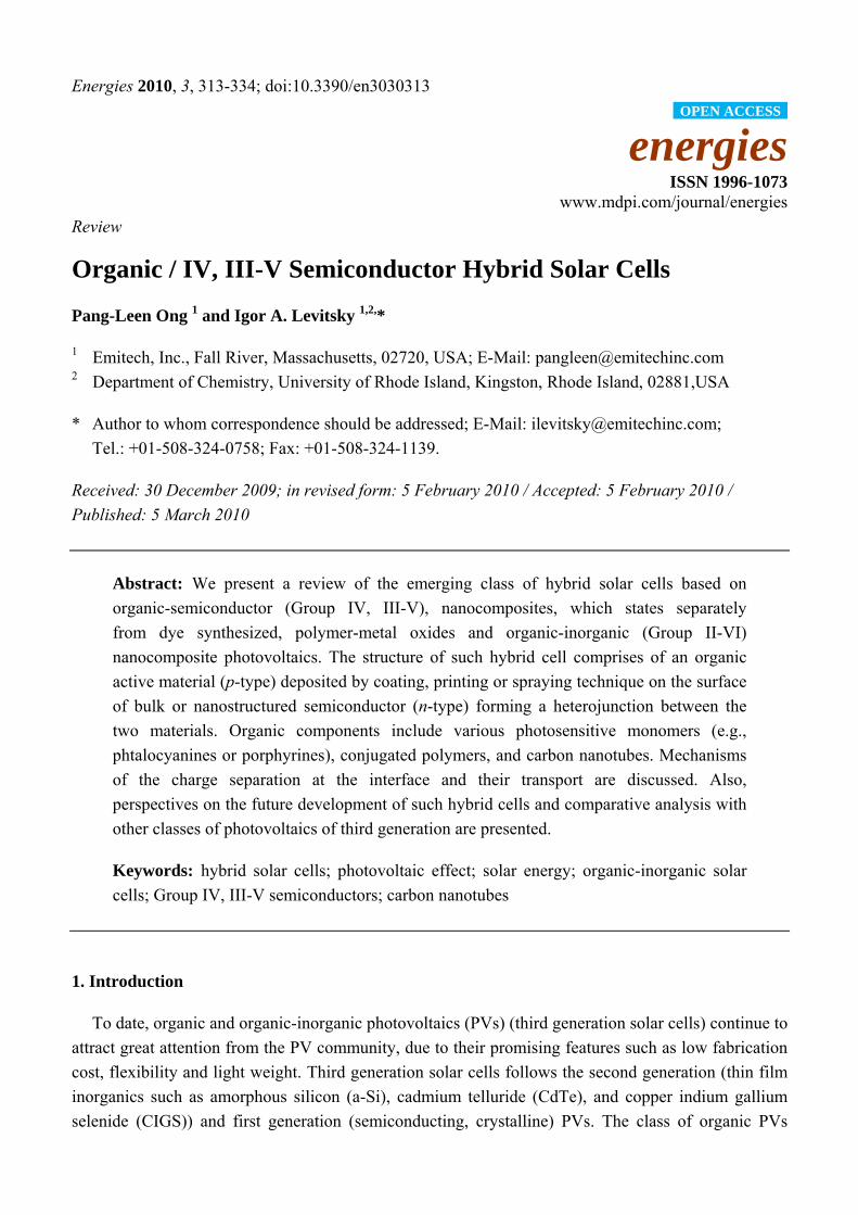
Figure 1 systemizes the types of hybrid PVs depending on the nature of organic and inorganic
component and the morphology of the devices. This review is focused on hybrid solar cells based on
Group IV (Si) and Group III-V (mostly GaAs) semiconductors forming the heterojunction with
various organic components. However, for generality purposes, we will briefly describe other types
of hybrid PVs.
Figure 1. Classification of hybrid solar cells.
Organic-Inorganic
Hybrid Solar Cells
Flat Surface
Small Molecules
Polymers Carbon Nanotubes
Blend of semiconducting nanoparticles/nanorods
with polymers
Metal Oxides - Organics
DSSC Porous MeOinfiltrated
with polymers
IV, III-V Semiconductors Organics
NanostructuredSurface
Dye-sensitized solar cells (DSSCs) [9,11] is probably the most well studied hybrid solar cells.
DSSC is composed of nanoporous metal oxide (usually TiO2) infiltrated with sensitized dye molecules
(ruthenium based “N3” dye) and liquid electrolyte. Photon absorption by the dye results in fast electron
transfer to the metal oxide followed by electron transport to the electrode (SnO2). Dye regeneration
occurs through the electron transfer from the liquid electrolyte. DSSC possess the highest conversion
efficiency (up to 11%) among organic and hybrid PVs [9,13]. The major factor contributing to the
enhanced efficiency is the highly mobile ions in the liquid electrolyte which rapidly compensates the
Coulomb interaction between photogenerated electron-hole pairs and thus minimizing the
recombination process at the interface. At the same time, the liquid electrolyte is the serious drawback
of DSSCs, making them problematic for future technology transition. Attempts to employ solid
electrolytes were not very successful and so far the highest reported conversion efficiency for solid
DSSC is only 4.5% [14].
Another class of hybrid PVs as shown in Figure 1 is similar to DSSC because of the same
nanoporous metal-oxide inorganic matrixes (e.g., TiO2, ZnO2) incorporated in the device architecture.
However, instead of employing dye or electrolyte, conjugated polymers (e.g., polythiophene
derivatives [10,12], or thiophene-fluorene copolymers [10,15]) function as the organic counterpart. It
was previously envisioned that such organic-inorganic system should be very efficient for charge
separation and carrier transport due to the large interfacial area between the nanoporous metal oxide
Energies 2010, 3
316
and the infiltrated polymer, as well as the relatively high carrier mobility in polythiophenes
(~0.1 cm2 V−1 s−1 [16]). Electron mobility in metal oxide semiconductors is significantly higher
(e.g., ~440 cm2V−1s−1 for ZnO [17]) than in organic systems. However, reported conversion efficiency
to date for these hybrid PVs are relatively low (~0.1–0.6%), which could be associated with the high
recombination rate at the interface (in contrast to DSSC) and the twisted conformation of polymers
inside the nanopores, leading to the reduction of hole mobility [10,12,18]. An interesting theoretical
model describing the factors limiting the efficiency of organic solar cells (hybrid metal-oxide/organic
PVs were included) was reported by Nelson et al. [19]. Note, that for metal oxide based hybrid PVs,
only the dye or the polymer component contributes to the photoconversion process while the inorganic
component provides the interface for charge separation and photocarrier transportation. Because of the
wide band gap (TiO2 ~ 3.1 eV; ZnO ~ 3.4 eV), metal oxide semiconductors cannot absorb solar light at
lower spectral energy.
Hybrid PVs based on inorganic nanoparticles (mostly Group II-VI) blended with conjugated
polymers (Figure 1) have been considered as a promising nanocomposite photosensitive materials for
the past decade [20]. High charge mobility in semiconducting colloidal nano-objects, contribution to
the solar light absorption (as distinct from the metal oxides based solar cells), bulk heterojunction and
easy wet processing could provide advantages over other hybrid and organic PVs. Nevertheless, their
conversion efficiency remains low in the range of 1–3%. The main reasons likely are the electrically
inactive network of colloidal nanoparticles/nanorods and the high interfacial recombination rate.
2. Hybrid Solar Cells Based on Flat Heterojunction Between Group IV, III-V Semiconductors
and Organics
2.1. Semiconductor—polymer solar cells
One of the first studies of Si-polymer solar cells was reported by Lewis et al. [21], describing a
device prepared by coating of poly-(CH3)3Si-cyclooctatetracene over crystalline Si surface with
reported conversion efficiency between 1% and 5%. The role of the polymer in the device design was
dual: providing an interface with n-type Si (nSi) for photocarriers separation and hole collection
through the polymer film to the external electrode. The polymer was doped with iodine vapors to
enhance the film conductivity. After doping, the polymer became relatively transparent to solar light,
thus only Si was involved in photocarrier generations. The achieved photovoltage (Voc = 0.64 V) was
in good agreement with theoretical calculations made for the case of negligibly low interfacial
recombination. The control device (Au/nSi-Schottky cell) showed Voc ~ 0.3 V, twice lower than the
theoretical limit. Historically, the first results about polymer-semiconductors heterojunction for PV
applications were reported in 1978 by McDiarmid group [22]. In this work, polyacetylene polymers
(p-type) were directly grown on an n-type ZnS semiconductor wafer. The quantum efficiency spectrum
showed a sizable response below the band gap energy (3.7 eV) of ZnS, which was attributed to the
polymer contributing to the photoconversion process. The short circuit current was very low (nA
range) as a result of the point contact between the electrode wire and the polymer surface.

Energies 2010, 3
317
Figure 2. Organic compounds commonly used to interface with Group IV,
III-V semiconductors. MEH-PPV is poly(2-methoxy-5-(2-ethyl-hexyloxy)1,4-
phenelynevinylene); P3HT is poly (3-hexylthiophene) ; P3MT is poly (3-methylthiophene);
TPP is tetraphenyl porphyrin.
S
Me
n
P3MT
* C C * n
polyacetylene
n
O
O
MEH-PPV
S
C6 H13
n
P3HT
SS
SS
SS
SS
octiethiophene
Me-Phtalocyanine
LC Me-Phtalocyanine
N
NH
NH
N
TPP
polyacetylene
CNT
Me-Phtalocyanine
MEH-PPV
P3HT
Octithiophene (8T)
TPP
Liquid Crystal Cu-Phtalocyanine
R = -O-C12H25
N N
N NCu
N
N N
R
R R
R
R
R
R
R
P3MT
Relatively recent studies of Si-polymer hybrids cells, as a rule, dealt with wet coating of conjugated
polymers on semiconductor surfaces [23-26]. McGehee et al. [23] investigated photovoltaic properties
of the heterojunction between amorphous Si (a-Si) and two conjugated polymers, P3HT and
MEH-PPV (Figure 2). Amorphous Si is attractive for PV applications because it is inexpensive and
can be deposited as a thin film over flexible metal substrates. Based on the photocurrent action spectra,
it was found that polymers instead of a-Si provide the major contribution to photoconversion process
despite the a-Si absorbing light in the visible/UV range of the solar spectrum. These intriguing results
demonstrate the substantial difference between inorganic a-Si solar cells (where a-Si is a photoactive
component) and hybrid devices when excitonic effects in polymers dominate over unbound photo
electron-hole pairs in amorphous semiconductor. The authors suggested two mechanisms of charge

Energies 2010, 3
318
separation at the a-Si/polymer interface: (i) exciton diffusion toward the interface, its dissociation and
electron injection to semiconductor; (ii) Forster like energy transfer from polymer to semiconductor
followed by backward hole injection in the polymer. Despite of the interesting approach for the
development of cost effective, thin film hybrid photovoltaics, conversion efficiencies were very low,
e.g., 0.16% for a-Si/P3HT and 0.01% for a-Si/MEH-PPV devices [23]. Some improvements in the
conversion efficiency were attained later by nanostructuring of a-Si surface [24] (see next section).
The replacement of amorphous Si with crystalline nSi in the similar device with P3HT resulted in
considerable enhancement of the conversion efficiency, up to 2.46% (60 mW/cm2) [26]. This could be
explained by the faster electron mobility, higher absorption in NIR/red spectral range, and lower
interfacial recombination in the crystalline Si as compared with amorphous Si.
Another class of hybrid solar cells with flat heterojunctions is GaAs/thiophene based polymers and
oligomers [27-30] (Figure 2). The first study of poly (2 metylthiphene) (PMeT)/GaAs based solar cell
was reported in 1986 by Horowitz and Garnier [27]. Later, an almost identical result was published by
Garnier in 2002 [28]. The top electrode in these devices was a thin Au layer sputtered on the polymer.
This circumstance added certain difficulties in interpreting the experimental results because of the PV
action for Au/nGaAs heterojunction, which is typical for Schottky barrier solar cells. Thus, although
the polymer insertion between Au and GaAs could improve the PV performance, which indeed was
observed, the real picture of photoconversion process at the presence of the two interfaces (Au/P3HT
and P3HT/nGaAs) is far from a complete understanding. Despite the authors claiming a conversion
efficiency of 17.5% (corrected on Au reflection), the actual values did not exceed 1% for a real
Au/P3HT/nGaAs based solar cell.
It is interesting that a similar device structure, where the P3HT polymer was replaced by thermally
evaporated rod-like octylthiophene (8T) (Figure 2) allows to elucidate the role of the film morphology
for efficient photoconversion [29]. Microcrystalline 8T films (deposited at 140 C, grain size 1–2 µm)
exhibited much higher conversion efficiency than nanocrystalline 8T films (deposited at 100 C, grain
size 0.1 µm). It was found that microcrystalline films provides better ordering of 8T oligomers leading
to the exciton diffusion length of several tens nanometers, while nanocrystalline film with low
ordering clearly demonstrated photocurrent losses presumably owing to the higher trap density (mostly
at the grain border). The best conversion efficiency for a Au/8T/nGaAs cell was 4.2%, corresponding
to an organic layer thickness of 20 nm. However, the power intensity was only 60 mW/cm2 and the Au
layer was doped with iodine vapors in order to increase the electrode conductivity. In contrast to study
[27] (where PMeT was photo-inactive), 8T layer definitely contributed to the photoconversion process.
2.2. Semiconductor—small molecules solar cells
The use of organic small molecules to form heterojunctions with semiconductors (mostly Si) for
hybrid PVs has been intensively studied for the past decade. In solar cell design, small molecules
could have advantages over polymers due to the higher molecular ordering (quasi–
crystalline/crystalline structure) and better environmental stability. In the crystal phase, charge
mobility (~0.2 cm2V−1s−1 [31]) can be comparable or even exceed the carrier mobility in polythiophene
based polymers (~0.1 cm2V−1s−1 [16]). The physical and chemical properties of organic molecules
selected should satisfy at least two major conditions: high absorption coefficient in the solar spectrum

Energies 2010, 3
319
and sufficient electrical conductivity in the solid state. A various derivatives of phtalocyanines (Pc)
and porphyrines (Ph) can be considered as promising candidates for the construction of the
heterojunction with semiconductors (Figure 2). Phtalocyanines and porphyrines (especially metal
substituted Pc (MePc)) have been well studied for molecular optoelectronic and electrophotography
applications. Pc and Ph demonstrated an excellent photoconductivity that allows for utilizing in the
design of various organic solar cells and photodetectors. Therefore, most of the reported studies of
semiconductor-small molecules hybrid cells are related to Pc and Ph compounds. In particular,
pSi/CuPc [32], Si/ZnPc [33,34], nSi/MgPc [35], pSi/NiPc [36], nGaAs/CuPc [37] and nSi/TTP [38]
(Figure 2) hybrid solar cells were reported in literature with conversion efficiencies in the range of 1–
3.5%. An additional advantage of phtalocyamines is their exceptional chemical stability. However, for
film deposition, the major amount of Pc and Ph compounds requires vacuum sublimation due to the
low solubility in organic solvents and water (except derivatives with long alkyloxy chains). This
circumstance is a serious drawback making it impossible to apply the simple and cost effective wet
processing for hybrid cell fabrication.
The physics of photovoltaic effect is far from a full understanding in terms of photocarrier
generation and separation. Surprisingly, none of these studies presented photocurrent action spectra.
Therefore, it is difficult to estimate the contribution of Si and organic component to the light
absorption and photoconversion. Only in study [35], the photocurrent spectrum of nSi/MgPc device
was detected, and matches well with the optical absorption of MgPc. This is indicative of the
dominating role of organic layer in the photoconversion process (note that the minimal thickness of
MgPc film was 170 nm, which could be sufficient to block the light for Si component). The analysis of
the optoelectronic properties for all of the above-mentioned diodes were based on p-n heterojunction
models applicable for inorganic semiconductors and neglecting the excitonic origin of photocarriers in
organic component. Despite such limitations, several important parameters were extracted from the
analysis of I-V and C-V characteristics. In particular, in almost all types of devices, it was found that
the predominant current mechanism (in forward direction) is trap assisted multistep tunneling. Also, all
of the solar cells demonstrated better PV performance than the control device (Au/Si solar cell) which
is indicative of the contribution of excitons generated in organic layer and the reduction of interfacial
trap density.
3. Hybrid Devices Composed from Nanostructured Semiconductors (Si, GaAs, InP, Ge)
and Organics
Recent progress in the nanostructuring of semiconductors opens a new opportunity for
improvements in the performance of hybrid solar cells. First of all, the quantum confinement
dramatically changes the opto-electronic properties of nanostructured semiconductor leading to the
tunable band gap, enhancement of the light absorption, and altered electrical conductivity depending
on the characteristic size at nanoscale environment. Such circumstance provides an additional
parameter (nanoscale tunability) for optimal compatibility between the organic and the inorganic
components in order to form heterojunctions with advanced PV characteristics. The morphology of the
heterojunction is also important as such devices have increased interfacial area and reduced average
distance from one point to an interface. As the separation of charge carriers occurs at interfaces

Energies 2010, 3
320
through exciton dissociation, such structures enhance it, and thus lead to an increase in the
photocurrent. Figure 3 presents the schematic demonstrating potential advantages of nanostructured
organic-inorganic interface over flat heterojunction. In terms of the efficiency of the organic layer in
the case of a flat heterojunction, the figure of merit can be formulated as F ~ Lex/Lab, where Lex is the
exciton diffusion length and Lab = 1/k is the light penetration length (k is the absorption coefficient).
Thus, thin organic layer with thickness of d ~ Lex and d < Lab, provides efficient charge separations (all
excitons reach the interface) but low absorbance (Figure 3a). In contrary, relatively thick organic layer
(Lab ~ d > Lex) absorbs more light energy, but only a fraction of the excitons are capable of dissociating
at the interface (Figure 3b). In the case of nanostructured semiconductor infiltrated with organics, the
characteristic length (average distance between pillars or pore diameter) can be comparable with the
exciton diffusion length, while the nanostructured layer can be thick enough to absorb substantial light
energy (Figure 3c). However, it should be noted that the large interface increases interfacial
recombination. As a rule, for many polymers and small molecules, Lex (several tens nm for singlet
excitons) is lower than Lab of several hundreds nm. Therefore, an optimal design of nanostructured
semiconductor could comprise of axial nanoobjects such as pillars or pores (better ordered) with an
average distance ~5–20 nm and length of 500–1,000 nm or longer.
Figure 3. Exciton (dots) generation in the hybrid structures with flat (a,b) and
nanostructured heterojunction (c).
hv hv hv
LexLex
Lab
LabLex
Lab
(a) (b) (c)
3.1. Nanowires and nanopillars
Recently, a new trend in hybrid photovoltaics emerges as a result of intensive efforts in the field of
nanowires/nanopilars growth from Group IV, III-V semiconductors. These nanostructures provides a
large interfacial surface in contact with the organic materials and can be easily fabricated by various
techniques such as chemical vapor deposition (CVD) [43], laser ablation [41], molecular beam epitaxy
(MBE) [42], dry etching [24]. Hybrid solar cells based on Si [39-41], GaAs [42], InP [43], Ge [44]
nanowires (NW) and polymers (mostly P3HT) has been reported in literature for the last 2–3 years.
Figure 4 shows the cross-sectional SEM image of ordered GaAs nanowires grown on n-type GaAs
substrate after infiltration with P3HT polymer [42]. The conversion efficiency of the cell with
ITO/P3HT-NW/GaAs/Me structure can be varied from <0.1% to 1.04% (2.6 sun) depending on the

Energies 2010, 3
321
P3HT solvent composition and the nanowire etching time (prior to deposition to remove the native
oxide). The control devices (nanowires without P3HT and P3HT without nanowires) demonstrated
negligible PV response, which is indicative of the importance of the nanostructured interface in the
device architecture.
Figure 4. Cross-sectional image of GaAs nanowires infiltrated with P3HT [42].
Reproduced with permission from the Institute of Physics and IOP Publishing
Limited, ©2009.
PV response of Si nanowires-P3HT interface has been investigated in study [39]. The NWs of
smaller sizes (3–5 nm) resulted in higher open-circuit voltage and higher short circuit current than
nanowires with larger diameters (10–20 nm) [39]. The authors suggested that a widening of the band
gap for smaller NWs decreases the conduction band offset between the Si NW and the P3HT leading
to reduced voltage loss during exciton dissociation. The highest conversion efficiency was 1.15% (1
sun) for Si NWs with diameters of 3–5 nm and 35 wt% ratio of NW to P3HT. In study [41], the Si
NWs were fabricated by etching process. Then, the NWs were pressed into P3HT layer followed by
removal of the wafer. The reported conversion efficiency of such device was 1.93%. In both studies
[39,41], the Si NWs definitely contributed in the photoconversion process by light harvesting in the
NIR range, where the polymer cannot absorb light energy.
A novel approach in the design of hybrid solar cells has been described in Ref. [43], where InP
nanowires were directly grown on ITO substrate. It was shown that Ohmic contacts were formed
between the NWs and the ITO layer, which is a substantial achievement compared to NW/polymer
blend sandwiched between two electrodes. In this case, the NWs provide a direct pathway for electron
transport and collection at the ITO electrode. PV response was improved by the passivation of the InP
surface with sulfur, which reduces nonradiactive recombination. However, the conversion efficiency
was low (<0.1%), likely because of the thick non-uniform P3HT (4–6 μm) layer prepared by drop
casting. At such thicknesses, charge transport through the polymer network cannot supply enough
holes to the external electrode due to low hole mobility and hole trapping ( Lab ~ d > Lex, Figure 3b).

Energies 2010, 3
322
Nanostructured surface of amorphous Si (a-Si), prepared by nanosphere lithography and reactive
ion etching, resulted in an improvement of the PV response for ITO/nanostructured a-Si/P3HT/Ag
device [24]. Such nanostructure can be presented as interconnected array of nanopillars with average
pore sizes of 30–40 nm. The conversion efficiency was increased up to 0.3% as compared with flat
heterojunctions (0.16%) [23]. The higher pillar height leads to enhancement of the short circuit current
and is likely associated with an increase of the surface interface between P3HT and a-Si.
3.2. Nanoporous wet etched structures
An alternative approach to nanowire growth is the use of nanoporous semiconductors fabricated by
electrochemical etching process (mostly porous Si, however porous GaAs and other III-V
semiconductors were also investigated [45]). The electrochemical etching of Si is a well known
technique for preparation of various porous structures with pore sizes from ~5–50 nm (mesoporous) to
several hundreds nanometers (macroporous) [46]. There are only a few reports about hybrid cells
based on mesoporous Si infiltrated with small molecules [47-49], however this fabrication method is
simple (wet processing as distinct from nanowire growth) and can obtain conversion efficiencies up to
~3% [48], exceeding those of nanowire based hybrid PVs [39-44].
In study [47], mesoporous n-type Si (PSi) was infiltrated with CuPC and its derivative discotic
liquid crystal CuPC (CuPCL) (Figure 2). The choice of CuPCL was motivated by the possibility of
increasing the hole mobility along the quasi-1D columns, similar to LC perylene derivatives [31]. It
was shown by A. Komolov et al. [50] that electron transfers from CuPC film to n-Si (100) substrates
extends a positively charged layer into the CuPC film up to 10 nm. Porous Si has several important
functions in hybrid solar cells. It serves as light absorber, antireflection coating and as nanostructured
material for electron transfer and transport. The CuPC provides the light absorption, charge separation
at the interface with PSi and hole transport medium. Figure 5 shows the SEM image of PSi prior to and
after infiltration with CuPC.
Contrary to anticipations, CuPCL based cells demonstrated significantly lower conversion
efficiency, ~0.01% (comparable with the control device—the same cell without organic components)
than solar cells infiltrated with CuPC with efficiencies up to 3%. Such striking differences can be
explained in terms of the interfacial area between the organic and the inorganic components.
Presumably, the electron transfer from CuPCL to Si is slow enough or is nonexistent due to relatively
long alkyloxy chains (Figure 2), which could prevent close contact of the CuPCL molecular core with
PSi. Thus, the critical issue becomes an average distance between a CuPC core to the PSi surface and
LC organization cannot compensate the low photoinduced electron transfer caused by the long
alkyloxy chains.

Energies 2010, 3
323
Figure 5. (a) SEM image of Si surface and cross-section after electrochemical
etching: 15% HF/ethanol solution, 20 s, 50 mA/cm2, the porous layer depth is 1,400 nm.
(b) The same sample after infiltration with CuPC/H2SO4 (cross-section only) [48].
Reproduced with permission from SPIE, ©2005.
(a) (b)
Figure 6. (a) I-V characteristics of the ITO/PSi-CuPC/Si/Cr/Au cells with different
thicknesses of PSi layer at white light illumination (33 mW/cm2): Circles: PSi layer
thickness is 1.8 µm: Isc = 7.40 mA/cm2, Voc = 0.237 V, FF = 29%, = 1.6%; Squares: PSi
layer depth is 12 µm (Isc = 7.56 mA/cm2, Voc = 0.325 V, FF = 40%, = 3%. (b) The
dependence of reflectivity of PSi layer with porosity 35% on its thickness at 650 nm [48].
Reproduced with permission from SPIE, ©2005.
-0.6 -0.4 -0.2 0.0 0.2 0.4 0.6-10
-5
0
5
10
15
20
Cu
rren
t d
ensi
ty, m
A/c
m2
Voltage, V
12 m thick PSi layer 1.8 m thick PSi layer
4 6 8 10 12
0.3
0.4
0.5
0.6
0.7
Ref
lect
ivit
y, a
.u.
Layer thickness, m
(a) (b)
In addition, the effect of porosity and layer thickness on PV performance was investigated [48]. The
I-V characteristics are shown in Figure 6a for two devices with different thickness of PSi layer. The
conversion efficiency was enhanced from 1.6% to 3% with an increase of the pore depth from 1.8 µm
to 12 µm. At the same time, the reflectivity drops from 80 % to 30%, measured at 650 nm (Figure 6b).
Thus, an increase of the conversion efficiency is most likely a result of reduced reflectivity of the
deeper porous layer. An efficient penetration depth of CuPC is about 200 nm according to XPS data,
Energies 2010, 3
324
which is indicative of potential for the following improvements of PV properties using deep and
uniform filling.
Two PSi samples with similar reflectance spectra but with different porosity (35% and 75%) were
employed to fabricate PV devices. It was found that the sample with lower porosity (35%) exhibits
higher conversion efficiency by an order of magnitude than the sample with higher porosity (75%).
Hence, the Si porosity plays a key role in the carrier transport, affecting the device performance [48].
According to study [51], as crystalline Si becomes porous, conductivity decreases because of the
strong dependence of the diffusion coefficient on the porosity value. When the porosity reaches 57%,
the conductivity of the PSi is dramatically reduced. This implies that the conductivity in PSi with
porosity higher then 57% is determined by a hopping mechanism between crystallites. Thus, an ideal
structure of the PSi layer for PV applications could be a low porous layer with sufficient thickness of
~10 μm and higher.
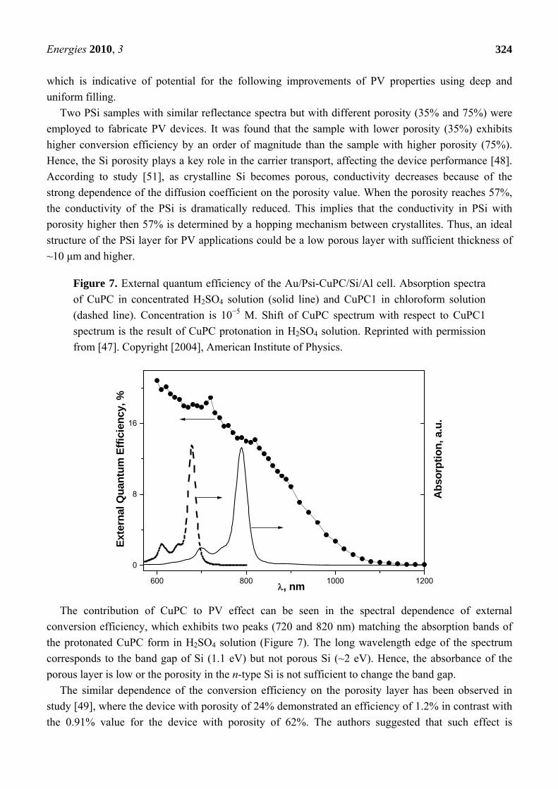
Figure 7. External quantum efficiency of the Au/Psi-CuPC/Si/Al cell. Absorption spectra
of CuPC in concentrated H2SO4 solution (solid line) and CuPC1 in chloroform solution
(dashed line). Concentration is 10−5 M. Shift of CuPC spectrum with respect to CuPC1
spectrum is the result of CuPC protonation in H2SO4 solution. Reprinted with permission
from [47]. Copyright [2004], American Institute of Physics.
600 800 1000 1200
0
8
16
Ab
sorp
tio
n, a
.u.
, nm
Ext
ern
al Q
uan
tum
Eff
icie
ncy
, %
The contribution of CuPC to PV effect can be seen in the spectral dependence of external
conversion efficiency, which exhibits two peaks (720 and 820 nm) matching the absorption bands of
the protonated CuPC form in H2SO4 solution (Figure 7). The long wavelength edge of the spectrum
corresponds to the band gap of Si (1.1 eV) but not porous Si (~2 eV). Hence, the absorbance of the
porous layer is low or the porosity in the n-type Si is not sufficient to change the band gap.
The similar dependence of the conversion efficiency on the porosity layer has been observed in
study [49], where the device with porosity of 24% demonstrated an efficiency of 1.2% in contrast with
the 0.91% value for the device with porosity of 62%. The authors suggested that such effect is
Energies 2010, 3
325
associated with the increased distance between CuPC and PSi surface for highly porous structure.
However, a more plausible explanation is related to the abrupt conductivity reduction for porosities
more than 57% [51].
4. Solar Cells Based on Silicon and Carbon Nanotubes
Despite significant achievements for the past decade, hybrid PVs from Group IV, III-V
semiconductors and organics (polymer and small molecules) still remain promising objects for future
research. Their conversion efficiency so far does not exceed the level of 3–4%, which is not sufficient
for any commercial applications. This situation however can soon be dramatically changed, as a result
of recent research related to PV properties of CNTs—Si heterojunction [52-56].
It is known that the major drawback of hybrid solar cells is insufficient PV quality of the organic
component, which is attributed to the low charge mobility, lack of absorbance in the red/NIR spectral
range, and chemical instability. On the other hand, the obvious advantages of organics are wet
processings, light weight and flexibility.
Remarkably, CNTs possess the above-mentioned advantage and are free from the mentioned
deficiency. Indeed, the unique optoelectronic properties of CNTs [57] make them a favorite candidate
compared to other organic materials for incorporating in the structure of hybrid solar cells. First, CNT
charge mobility can be up to 105 cm2V−1s−1 for individual nanotubes [58] and ~60 cm2V−1s−1 for CNT
films [59], which is much higher than the hole mobility in P3HT polymer (one of the best organic
conductor). Second, CNTs has a high light absorbance in the red and NIR spectrum (absorbance
coefficient of 10−4–10−5 cm−1). Third, they exhibit an exceptional environmental stability. Fourth,
carbon nanotubes can be deposited easily to the semiconductor surface by wet processing techniques
(coating, spraying, and printing). Finally, CNTs can be easily doped or functionalized, thus tuning the
Fermi level to the favorable position when forming heterojunction with semiconductors [60-62].
The photoconductive response of films prepared from single walled carbon nanotube (SWNT)
under laser pulse excitation was first reported by Fujiwara et al. [63]. Subsequently, photocurrent
response of SWNT film under continuous wave illumination were reported by Levitsky et al. (SWNT
films) [64] and for individual SWNT bundle by Freitag et al. [65]. It is important that the combination
of CNTs of varying diameters and chiralities, and correspondingly different band gap (the band gap is
inversely proportional to diameters) makes it theoretically possible to obtain a continuous
photoresponse over a broad spectral range covering the red and NIR part of the solar spectrum.
For the past decade, applications of CNTs in organic solar cells were mostly focused as nanoscale
fillers for polymer films [66-71]. The donor-acceptor configuration, where the high aspect ratio and
large surface area of nanotubes incorporated in these polymers was believed to be favorable for higher
exciton dissociation and increased charge carrier transport. However, the power conversion efficiency
for these structures remains relatively low (<1%) possibly due to the low carrier mobility in polymers
and poor dispersion of CNTs in polymer matrix. Another way to employ CNTs in solar cell design is
the use of CNTs as a transparent conductive coating to replace metal oxides electrodes (e.g., ITO) for
organic PVs [62,73]. Nevertheless, little progress has been achieved in this direction as the
conductivity of the CNT network is still lower than the conductivity of ITO at the same transparency
level in the visible spectral range.
Energies 2010, 3
326
Very recently several groups reported the hybrid solar cells based on heterojunction of CNTs and
n-type Si [52-56] where CNTs function as active photosensing component being involved in the light
absorption, charge separation and charge transport. Surprisingly, only for the past two years, the
conversion efficiency of such devices exceed the level of 7% [54] and are very promising for even
higher conversion efficiency with special CNTs treatments and device optimizations.
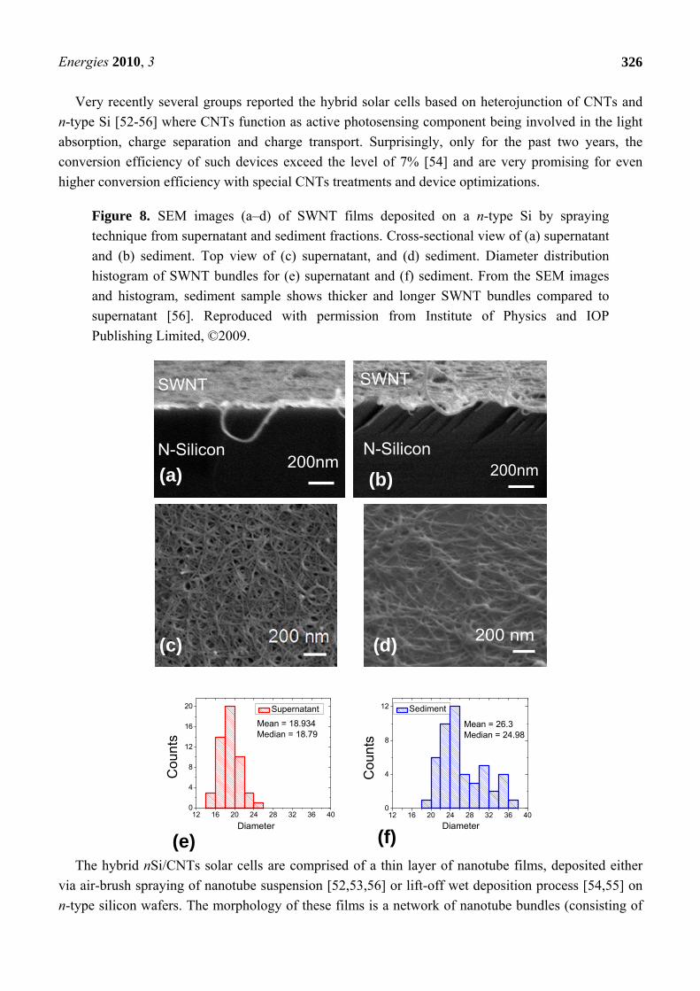
Figure 8. SEM images (a–d) of SWNT films deposited on a n-type Si by spraying
technique from supernatant and sediment fractions. Cross-sectional view of (a) supernatant
and (b) sediment. Top view of (c) supernatant, and (d) sediment. Diameter distribution
histogram of SWNT bundles for (e) supernatant and (f) sediment. From the SEM images
and histogram, sediment sample shows thicker and longer SWNT bundles compared to
supernatant [56]. Reproduced with permission from Institute of Physics and IOP
Publishing Limited, ©2009.
200nmN-Silicon
SWNT
200nmN-Silicon
SWNT
12 16 20 24 28 32 36 400
4
8
12
Mean = 26.3Median = 24.98
Cou
nts
Diameter
Sediment
200 nm200 nm
(b)
(c) (d)
(e) (f)12 16 20 24 28 32 36 40
0
4
8
12
16
20
Cou
nts
Diameter
Supernatant
Mean = 18.934Median = 18.79
200nmN-Silicon
SWNT
200nmN-Silicon
SWNT
(a)
The hybrid nSi/CNTs solar cells are comprised of a thin layer of nanotube films, deposited either
via air-brush spraying of nanotube suspension [52,53,56] or lift-off wet deposition process [54,55] on
n-type silicon wafers. The morphology of these films is a network of nanotube bundles (consisting of

Energies 2010, 3
327
several tens of individual nanotubes) with highly porous structure (Figure 8c,d). Because
semiconducting single walled nanotubes (SWNTs) and double walled nanotubes (DWNTs) are
naturally p-type conductors, when interfaced with n-type Si, they form p-n heterojunctions. I-V
measurements of nSi/SWNT heterojunction [56] exhibit typical solar cell characteristics under dark
and under light illumination (Figure 9a). Such rectifying behavior can be explained by the schematic
energy band diagram based on Anderson model as shown in Figure 9b. As shown in the band diagram,
a large built in electric field is formed at the interface. The source of photocarriers in SWNTs is
excitons with a binding energy ~0.4 eV [74], which are dissociated at the interface due to the built-in
field. It is likely that the electrons then tunnel to the Si layer and holes are transported through the
SWNT network to the external electrode. Photogenerated free carries in Si can also be separated at the
interface followed by photohole injection from Si to SWNTs.
Figure 9. (a) Current-Voltage (I-V) plot of sediment and supernatant SWNT/nSi devices
under dark and light illumination. (b) Schematic energy band diagram of SWNT/nSi
heterojunction based on the Anderson model. Electron affinity, and conduction band
offset, ΔEc for SWNT and nSi are shown in the energy band diagram [56]. Reproduced
with permission from Institute of Physics and IOP Publishing Limited, ©2009.
-1.0 -0.5 0.0 0.5 1.0-40
-20
0
20
40
60
Cu
rren
t D
ensi
ty, J G
(m
A/c
m2)
Voltage (V)
Dark Sediment Light Sediment Dark Supernatant Light Supernatant
________________
______________
_______________________________________________
SWNT N-type Silicon
electron
hole
0.88eV ||||||||||||||||
0.68 eV
∆EC = 0.35 eV
= 4.01eV
= 4.56 eV
(a) (b)-1.0 -0.5 0.0 0.5 1.0
-40
-20
0
20
40
60
Cu
rren
t D
ens
ity
, J (
mA
/cm
2 )
Voltage (V)
Dark Sediment Light Sediment Dark Supernatant Light Supernatant
(b)(a)
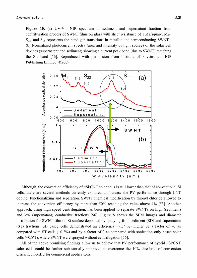
The role of SWNTs in photoconversion efficiency of the hybrid cell was not clearly understood in
studies [52,53,55] as no photocurrent action spectra were recorded. The first measurement of
photocurrent spectra showed maximum quantum efficiency peak at 1.2 eV, which is close to the
energy gap of Si (1.12 eV) [54], however a low resolution did not allow to identify the possible band
responsible for DWNT absorption and photoconversion. Later, Levitsky et al. [56] demonstrated a
matching photocurrent band of the nSi/SWNT device to the first transition band of the NIR absorption
spectra of the SWNT film (Figure 10). Thus, the CNTs in the hybrid nSi/CNT heterojunction solar
cells contribute to the photo conversion process not only as a charge separator/transporter/collector but
also as a light absorber. This is an important fact, distinguishing between a heterojunction solar cell
with two active light absorbing components and a Schottky cell, where the metal component is not
capable of absorbing photons.
Energies 2010, 3
328
Figure 10. (a) UV-Vis NIR spectrum of sediment and supernatant fraction from
centrifugation process of SWNT films on glass with sheet resistance of 1 k/square. M11,
S22, and S11 represents the band-gap transitions in metallic and semiconducting SWNTs.
(b) Normalized photocurrent spectra (area and intensity of light source) of the solar cell
devices (supernatant and sediment) showing a current peak band (due to SWNT) matching
the S11 band [56]. Reproduced with permission from Institute of Physics and IOP
Publishing Limited, ©2009.
4 0 0 6 0 0 8 0 0 1 0 0 0 1 2 0 0 1 4 0 0 1 6 0 0 1 8 0 0
0 . 0 1
0 . 1
1
N
orm
aliz
ed P
ho
toc
urr
ent
(a. u
.)
W a v e l e n g t h ( n m )
S e d i m e n t S u p e r n a t a n t
S i + S W N T
S W N T
4 0 0 6 0 0 8 0 0 1 0 0 0 1 2 0 0 1 4 0 0 1 6 0 0 1 8 0 00 . 0 0
0 . 0 4
0 . 0 8
0 . 1 2
0 . 1 6
8 , 6
7 , 6
8 , 6
Ab
sorb
ance
(o
ptic
al d
ensi
ty)
S e d im e n t S u p e r n a t a n t
7 , 6M11 S22 S11 (a)
(b)
Although, the conversion efficiency of nSi/CNT solar cells is still lower than that of conventional Si
cells, there are several methods currently explored to increase the PV performance through CNT
doping, functionalizing and separation. SWNT chemical modification by thionyl chloride allowed to
increase the conversion efficiency by more than 50% reaching the value above 4% [53]. Another
approach, using high speed centrifugation, has been applied to separate SWNTs on high (sediment)
and low (supernatant) conductive fractions [56]. Figure 8 shows the SEM images and diameter
distribution for SWNT film on Si surface deposited by spraying from sediment (SD) and supernatant
(ST) fractions. SD based cells demonstrated an efficiency (~1.7 %) higher by a factor of ~8 as
compared with ST cells (~0.2%) and by a factor of 2 as compared with sonication only based solar
cells (~0.8%), where SWNT were sprayed without centrifugation [56].
All of the above promising findings allow us to believe that PV performance of hybrid nSi/CNT
solar cells could be further substantially improved to overcome the 10% threshold of conversion
efficiency needed for commercial applications.

Energies 2010, 3
329
5. Summary and Strategies to Improve PV Performance of Hybrid Solar Cells
Much progress for the past decade has been made towards making hybrid solar cells with advanced
PV properties. Up until recent years, pure organic PVs led in competition with hybrid devices,
demonstrating higher efficiency (up to 6.5% [5]) over 3–4% for various organic-inorganic structures.
However, it seems that organic P3HT: PCBM (or CuPC: C60) based devices have already exhausted
their potential as no significant progress were achieved for the past two years. Contrary, an efficiency
of 7.4% [54] which was reported in 2008 for hybrid Si/CNTs based solar cells opened new
opportunities to overcome the critical barrier of 10% efficiency. This finding and other promising
recent results [52,53,55,56] suggest to revisit the role of Si and Group III-V semiconductors
as inorganic component for hybrid PVs that currently employ mostly metal oxides
and II-VI semiconductors.
Silicon (the most widely used semiconductor in solar cell industry) can be easily integrated in the
hybrid cell design, not only as a crystalline component but also as microcrystalline, amorphous and
porous structure. Non-crystalline Si still maintains high charge mobility exceeding mobilities of most
organic compounds. At the same time, Si can be prepared as thin films by CVD (amorphous Si) or
electrochemical etching (mesoporous Si membrane). Figure 11 shows the SEM and photo images of
lightweight mesoporous Si membrane. Such membrane infiltrated with polymers can attain an
excellent flexibility [75] comparable with many plastic substrates. Furthermore, porous Si allows
introducing photonic bandgap structure in the device, reducing reflection and increasing light trapping,
which is of utmost importance for thin film PVs.
Figure 11. (a) SEM image of the freestanding PSi membrane fabricated in 15%
HF/ethanol solution at 50 mA/cm2 current density and electrochemically separated from
the substrate using 250 mA/cm2 current density [48]. Reproduced with permission from
SPIE, ©2005. (b) Photo image demonstrating the PSi membrane fabricated at Emitech, Inc.
(a) (b)
Developing novel organic materials with high hole mobilities and enhanced light absorbance in the
broad spectral range might be the other promising direction to achieve high short circuit current and
open circuit voltage. One of the best candidates for that purpose could be CNTs which have already
demonstrated an excellent PV performance when interfaced with Si. Figure 12 shows a hypothetical
schematic of a near ideal hybrid solar cells including (i) thin film (mesoporous Si membrane); (ii) 1-D
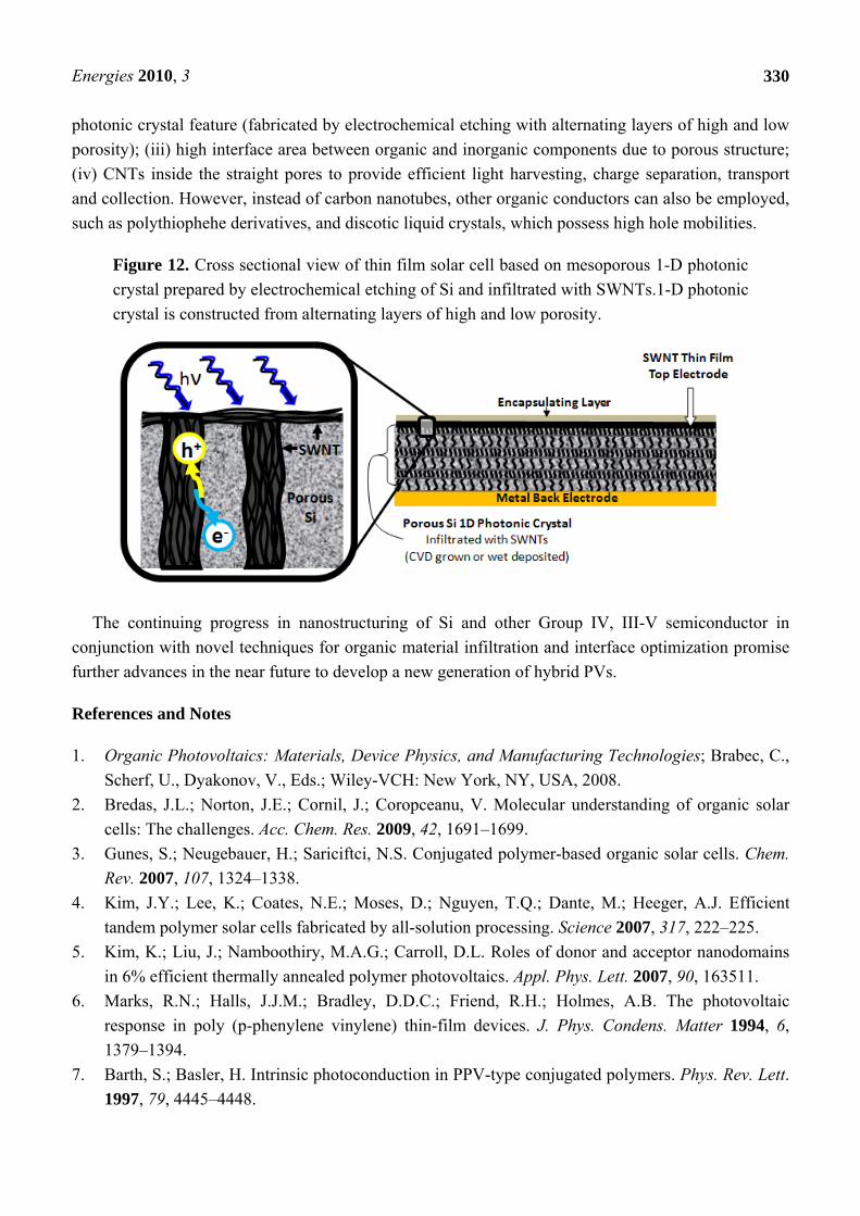
Energies 2010, 3
330
photonic crystal feature (fabricated by electrochemical etching with alternating layers of high and low
porosity); (iii) high interface area between organic and inorganic components due to porous structure;
(iv) CNTs inside the straight pores to provide efficient light harvesting, charge separation, transport
and collection. However, instead of carbon nanotubes, other organic conductors can also be employed,
such as polythiophehe derivatives, and discotic liquid crystals, which possess high hole mobilities.
Figure 12. Cross sectional view of thin film solar cell based on mesoporous 1-D photonic
crystal prepared by electrochemical etching of Si and infiltrated with SWNTs.1-D photonic
crystal is constructed from alternating layers of high and low porosity.
The continuing progress in nanostructuring of Si and other Group IV, III-V semiconductor in
conjunction with novel techniques for organic material infiltration and interface optimization promise
further advances in the near future to develop a new generation of hybrid PVs.
References and Notes
1. Organic Photovoltaics: Materials, Device Physics, and Manufacturing Technologies; Brabec, C.,
Scherf, U., Dyakonov, V., Eds.; Wiley-VCH: New York, NY, USA, 2008.
2. Bredas, J.L.; Norton, J.E.; Cornil, J.; Coropceanu, V. Molecular understanding of organic solar
cells: The challenges. Acc. Chem. Res. 2009, 42, 1691–1699.
3. Gunes, S.; Neugebauer, H.; Sariciftci, N.S. Conjugated polymer-based organic solar cells. Chem.
Rev. 2007, 107, 1324–1338.
4. Kim, J.Y.; Lee, K.; Coates, N.E.; Moses, D.; Nguyen, T.Q.; Dante, M.; Heeger, A.J. Efficient
tandem polymer solar cells fabricated by all-solution processing. Science 2007, 317, 222–225.
5. Kim, K.; Liu, J.; Namboothiry, M.A.G.; Carroll, D.L. Roles of donor and acceptor nanodomains
in 6% efficient thermally annealed polymer photovoltaics. Appl. Phys. Lett. 2007, 90, 163511.
6. Marks, R.N.; Halls, J.J.M.; Bradley, D.D.C.; Friend, R.H.; Holmes, A.B. The photovoltaic
response in poly (p-phenylene vinylene) thin-film devices. J. Phys. Condens. Matter 1994, 6,
1379–1394.
7. Barth, S.; Basler, H. Intrinsic photoconduction in PPV-type conjugated polymers. Phys. Rev. Lett.
1997, 79, 4445–4448.
Energies 2010, 3
331
8. Grahn, H.T. Introduction to Semiconductor Physics; World Scientific Publishing Company:
Singapore, 1999.
9. Gratzel, M. Dye-sensitized solar cells. J. Photochem. Photobiol. C 2003, 4, 145–153.
10. Boucle, J.; Ravirajan, P.; Nelson, J. Hybrid polymer-metal oxide thin films for photovoltaic
applications. J. Mater. Chem. 2007, 17, 3141–3153.
11. Gledhill, S.E.; Scott, B.; Gregg, B.A. Organic and nano-structured composite photovoltaics: An
overview. J. Mater. Res. 2005, 20, 3167–3179.
12. McGehee, M.D. Nanostructured organic-inorganic hybrid solar cells. Mater. Res. Soc. Bull. 2009,
34, 95–100.
13. Chiba, Y.; Islam, A.; Watanabe, Y.; Komiya, R.; Koide, N.; Han, L. Dye–sensitized solar cells
with conversion efficiency of 11.1%. Jpn. J. Appl. Phys. 2006, 45, L638–L640.
14. Wang, M.; Moon, S.; Xu, M.; Chittibabu, K.; Wang, P.; Cevey-Ha, M.; Humphry-Baker, R.;
Zakeeruddin, S.M.; Graetzel, M. Efficient and stable solid-state dye-sensitized solar cells based
on a high-molar-extinction-coefficient sensitizer. Small 2009, (in press).
15. Ravirajan, P.; Haque, S.A.; Durrant, J.R.; Poplavskyy, D.; Bradley, D.D.C.; Nelson, J. Hybrid
nanocrystalline TiO2 solar cells with a fluorene–thiophene copolymer as a sensitizer and hole
conductor. J. Appl. Phys. 2004, 95, 1473–1480.
16. Bao, Z.; Dodabalapur, A.; Lovinger, A.J. Soluble and processable regioregular
poly(3-hexylthiophene) for thin film field-effect transistor applications with high mobility. Appl.
Phys. Lett. 1996, 69, 4108–4110.
17. Makino, T.; Segawa, Y.; Tsukazaki, A.; Ohtomo, A.; Kawasaki, M. Electron transport in ZnO thin
films. Appl. Phys. Lett. 2005, 87, 022101.
18. Antoniadou, M.; Stathatos, E.; Boukos, N.; Stefopoulos, A.; Kallitsis, J.; Krebs, F.C.; Lianos, P.
Study of hybrid solar cells made of multilayer nanocrystalline titania and poly(3-octylthiophene)
or poly-(3-(2-methylhex-2-yl)-oxycarbonyldithiophene). Nanotechnology 2009, 20, 495201.
19. Nelson, J.; Kirkpatrick, J.; Ravirajan, P. Factors limiting the efficiency of molecular photovoltaic
devices. Phys. Rev. B 2004, 69, 035337.
20. Huynh, W.U.; Dittmer, J.J.; Alivisatos, A.P. Hybrid nanorod-polymer solar cells. Science 2002,
295, 2425–2427.
21. Sailor, M.J.; Ginsburg, E.J.; Gorman, C.B.; Kumar, A.; Grubbs, R.H.; Lewis, N.S. Thin films of
n-Si/Poly-(CH3)3Si-cyclooctatetraene: conducting-polymer solar cells and layered structures.
Science 1990, 249, 1146–1149.
22. Ozaki, M.; Peebles, D.L.; Weinberger, B.R.; Chiang, C.K.; Gau, S.C.; Heeger, A.J.; McDiarmid,
A.G. Junction formation with pure and doped polyacetylene. Appl. Phys. Lett. 1979, 35, 83–85.
23. Govrishankar, V.; Scully, S.R.; McGehee, M.D.; Wang, Q.; Branz, H.M. Exciton splitting and
carrier transport across the amorphous-silicon/polymer solar cell interface. Appl. Phys. Lett. 2006,
89, 252102.
24. Govrishankar, V.; Scully, S.R.; Chan, A.T.; McGehee, M.D.; Wang, Q.; Branz, H.M. Exciton
harvesting, charge transfer, and charge-carrier transport in amorphous-silicon nanopillar/polymer
hybrid solar cells. J. Appl. Phys. 2008, 103, 064511.
Energies 2010, 3
332
25. Alet, P.J.; Palacin, S.; Roca, P.; Cabarrocas, I.; Kalache, B.; Firon, M.; de Bettignies, R. Hybrid
solar cells based on thin-film silicon and P3HT—A first step towards nano-structured devices.
Eur. Phys. J. Appl. Phys. 2007, 36, 231–234.
26. Matsumoto, Y.; Estrada, M.; Nolasco, J.C. Performance of P3HT/c-Si hybrid solar cell. In
Proceedings of the 33rd IEEE Photovoltaic Specialists Conference, San Diego, CA, USA,
May 2008.
27. Horowitz, G.; Garnier, F. Polythiophene-GaAs p-n heterojunction solar cells. Sol. Energy Mater.
Sol. Cells 1986, 13, 47–55.
28. Garnier, F. Hybrid organic-on-inorganic photovoltaic devices. J. Opt. A: Pure Appl. Opt. 2002, 4,
S247–S251.
29. Ackermann, J.; Videlot, C.; Kassmi, A.E.; Guglielmetti, R.; Fages, F. Highly efficient hybrid solar
cells based on an octithiophene-GaAs heterojunction. Adv. Funct. Mater. 2005, 15, 810–817.
30. Ackerman, J.; Videlot, C.; Kasami, A.E. Growth of organic semiconductors for hybrid solar cell
application. Thin Solid Films 2002, 403, 157–161.
31. Schmidt-Mende, L.; Fechtenkotter, A.; Mullen, K.; Moons, E.; Friens, R.H.; MacKenzie, J.D.
Self-organized discotic liquid crystals for high-efficiency organic photovoltaics. Science 2001,
293, 1119–1122.
32. Antohe, S.; Tomozeiu, N.; Gogonea, S. Properties of the organic-on-inorganic semiconductor
barrier contact diodes in/PTCDI/p-Si and Ag/CuPc/p-Si. Phys. Status Solidi A 1991, 125,
397–408.
33. Remaki, B.; Guillaud, G.; Mayes, D. Space charge analysis in doped zinc phthalocyanine thin
films. Opt. Mater. 1998, 9, 240–244.
34. El-Nahass, M.M.; Zeyada, H.M.; Aziz, M.S.; El-Ghamaz, N.A. Carrier transport mechanisms and
photovoltaic properties of Au/p-ZnPc/p-Si solar cell. Solid-State Electron. 2005, 49, 1314–1319.
35. Riad, S. Dark and photoelectric conversion properties of p-MgPc/n-Si (organic/inorganic)
heterojunction cells. Thin Solid Films 2000, 370, 253–257.
36. El-Nahass, M.M.; Abd-El-Rahman, K.F.; Farag, A.A.M.; Darwish, A.A. Photovoltaic properties
of NiPc/p-Si (organic/inorganic) heterojunctions. Org. Electron. 2005, 6, 129–136.
37. Karimov, K.; Ahmed, M.M.; Moiz, S.A.; Fedorov, M.I. Temperature-dependent properties of
organic-on-inorganic Ag/p-CuPc/n-GaAs/Ag photoelectric cell. Sol. Energy Mater. Sol. Cells
2005, 87, 61–75.
38. El-Nahass, M.M.; Zeyada, H.M.; Aziz, M.S.; Makhlouf, M.M. Current transport mechanisms and
photovoltaic properties of tetraphenylporphyrin/n-type silicon heterojunction solar cell. Thin Solid
Films 2005, 492, 290–297.
39. Kuo, C.Y.; Gau, C. Arrangement of band structure for organic-inorganic photovoltaics embedded
with silicon nanowire arrays grown on indium tin oxide glass. Appl. Phys. Lett. 2009, 95, 053302.
40. Liu, C.Y.; Holman, Z.C.; Kortshagten, U.R. Hybrid solar cells from P3HT and silicon
nanocrystals. Nano Lett. 2009, 9, 449–452.
41. Huang, J.S.; Hsiao, C.Y.; Syu, S.J.; Chao, J.J.; Lin, C.F. Well-aligned single-crystalline silicon
nanowire hybrid solar cells on glass. Sol. Energy Mater. Sol. Cells 2009, 93, 621–624.
42. Bi, H.; LaPierre, R.R. A GaAs nanowire/P3HT hybrid photovoltaic device. Nanotechnology 2009,
20, 465205.
Energies 2010, 3
333
43. Novotny, C.J.; Yu, E.T.; Yu, P.K.L. InP nanowire/polymer hybrid photodiode. Nano Lett. 2008, 8,
775–779.
44. Du Pasquier, A.; Mastrogiovanni, D.D.T.; Klein, L.A.; Wang, T.; Garfunkel, E. Photoinduced
charge transfer between poly (3-hexylthiophene) and germanium nanowires. Appl. Phys. Lett.
2007, 91, 183501.
45. Christophersen, M.; Langa, S.; Carstensen, J.; Tiginyanu, I.M.; Foll, H. A comparison of pores in
silicon and pores in III-V compound materials. Phys. Status Solid. A 2003, 197, 197–203.
46. Canham, L.T. Properties of Porous Silicon; IEE/Inspec: London, UK, 1997.
47. Levitsky, I.A.; Euler, W.B.; Tokranova, N.; Xu, B.; Castracane, J. Hybrid solar cells based on
porous Si and copper phthalocyanine derivatives. Appl. Phys. Lett. 2004, 85, 6245–6247.
48. Tokranova, N.; Levitsky, I.A.; Xu, B.; Castracane, J.; Euler, W.B. Hybrid solar cells based on
organic material embedded into porous silicon. In Proceedings of the SPIE: Organic Photonic
Materials and Devices VII, San Jose, CA, USA, January 2005; pp.183–190.
49. Prabakaran, R.; Fortunato, E.; Martins, R.; Ferreira, I. Fabrication and characterization of hybrid
solar cells based on copper phthalocyanine/porous silicon. J. Non-Cryst. Solids 2008, 354,
2892–2896.
50. Komolov, A.S.; Moller, P. Electronic charge distribution at interfaces between Cu-phthalocyanine
films and semiconductor surfaces. Surf. Sci. 2003, 532–535, 1004–1010.
51. Aroutiounian, V.M.; Ghulinyan, M.Z. Electrical conductivity mechanisms in porous silicon. Phys.
Status Solidi A 2003, 197, 462–466.
52. Li, Z.; Kunets, V.P.; Saini, V.; Xu, Y.; Dervishi, E.; Salamo, G.J.; Biris, A.R.; Biris, A.S. SOCl2
enhanced photovoltaic conversion of single wall carbon nanotube/n-silicon heterojunctions. Appl.
Phys. Lett. 2008, 93, 243117.
53. Li, Z.; Kunets, V.P.; Saini, V.; Xu, Y.; Dervishi, E.; Salamo, G.J.; Biris, A.R.; Biris, A.S.
Light-harvesting using high density p-type single wall carbon nanotube/n-type silicon
heterojunctions. ACS Nano 2009, 6, 1407–1414.
54. Jia, Y.; Wei, J.; Wang, K.; Cao, A.; Shu, Q.; Gui, X.; Zhu, Y.; Zhuang, D.; Zhang, G.; Ma, B.;
Wang, L.; Liu, W.; Wang, Z.; Luo, J.; Wu, D. Nanotube–silicon heterojunction solar cells.
Adv. Mater. 2008, 20, 4594–4598.
55. Wei, J.; Jia, Y.; Shu, Q.; Gu, Z.; Wang, K.; Zhuang, D.; Zhang, G.; Wang, Z.; Luo, J.; Cao, A.;
Wu, D. Double-walled carbon nanotube solar cells. Nano Lett. 2007, 7, 2317–2321.
56. Ong, P.L.; Euler, W.B.; Levitsky, I.A. Hybrid solar cells based on single-walled carbon
nanotubes/Si heterojunction. Nanotechnology 2010, 21, 105203.
57. Dresselhaus, M.S.; Dresselhaus, G.; Eklund, P.C. Science of Fullerenes and Carbon Nanotubes;
Academic Press: San Diego, CA, USA, 1996.
58. Durkop, T.; Getty, S.A.; Cobas, E.; Fuhrer, M.S. Extraordinary mobility in semiconducting
carbon nanotubes. Nano Lett. 2004, 4, 35–39.
59. Xiao, K.; Liu, Y.; Hu, P.; Yu, G.; Wang, X.; Zhu, D. High-mobility thin-film transistors based on
aligned carbon nanotubes. Appl. Phys. Lett. 2003, 83, 150–152.
60. Sankapal, B.R.; Setyowati, K.; Chen, J. Electrical properties of air-stable, iodine-doped
carbon-nanotube-polymer composites. Appl. Phys. Lett. 2007, 91, 173103.
Energies 2010, 3
334
61. Lee, R.S.; Kim, H.J.; Fischer, J.E.; Thess, A.; Smalley, R.E. Conductivity enhancement in
single-walled carbon nanotube bundles doped with K and Br. Nature 1997, 388, 255–257.
62. Chen, J.; Hamon, M.A.; Hu, H.; Chen, Y.; Rao, A.M.; Eklund, P.C.; Haddon, R.C. Solution
properties of single-walled carbon nanotubes. Science 1998, 282, 95–98.
63. Fujiwara, A.; Matsuoka, Y.; Suematsu, H.; Ogawa, N.; Mitano, K.; Katahura, H.; Maniwa, Y.;
Suzuki, S.; Achiba, Y. Photoconductivity in semiconducting single-walled carbon nanotubes.
Jpn. J. Appl. Phys. 2001, 40, L1229–L1231.
64. Levitsky, I.A.; Euler, W.B. Photoconductivity of single wall carbon nanotubes under CW NIR
illumination. Appl. Phys. Lett. 2003, 83, 1857–1859.
65. Freitag, M.; Martin, Y.; Misewich, J.A.; Martel, R.; Avouris, P. Photoconductivity of single
carbon nanotubes. Nano Lett. 2003, 3, 1067–1071.
66. Geng, J.; Zeng, T. Influence of single-walled carbon nanotubes induced crystallinity enhancement
and morphology change on polymer photovoltaic devices. J. Am. Chem. Soc. 2006, 128,
16827–16833.
67. Pradhan, B.; Batabyal, S.K.; Pal, A.J. Functionalized carbon nanotubes in donor/acceptor-type
photovoltaic devices. Appl. Phys. Lett. 2006, 88, 093106.
68. Landi, B.J.; Raffaelle, R.P.; Castro, S.L.; Bailey, S.G. Single-wall carbon nanotube-polymer solar
cells. Prog. Photovolt. Res. Appl. 2005, 13, 165–172.
69. Ago, H.; Petritsch, K.; Shaffer, M.S.P.; Windle, A.H.; Friend, R.H. Composites of carbon
nanotubes and conjugated polymers for photovoltaic devices. Adv. Mater. 1999, 11, 1281–1285.
70. Bhattacharyya, S.; Kymakis, E.; Amaratunga, G.A. Photovoltaic properties of dye functionalized
single-wall carbon nanotube/conjugated polymer devices. Chem. Mater. 2004, 16, 4819–4823.
71. Kymakis, E.; Koudoumas, E.; Franghiadakis, I.; Amaratunga, G.A. Post-fabrication annealing
effects in polymer-nanotube photovoltaic cells. J. Phys. D: Appl. Phys. 2006, 39, 1058–1062.
72. Rowell, M.W.; Topinka, M.A.; McGehee, M.D.; Prall, H.J.; Dennler, G.; Sariciftci, N.S.; Hu, L.;
Gruner, G. Organic solar cells with carbon nanotube network electrodes. Appl. Phys. Lett. 2006,
88, 233506.
73. Van de Lagemaat, J.; Barnes, T.M.; Rumbles, G.; Shaheen, S.E.; Coutts, T.J.; Weeks, C.;
Levitsky, I.; Peltola, J.; Glatkowski, P. Organic solar cells with carbon nanotubes replacing
In2O3:Sn as the transparent electrode. Appl. Phys. Lett. 2006, 88, 233503.
74. Wang, F.; Dukovic, G.; Brus, L.E.; Heintz, T. The optical resonances in carbon nanotubes arise
from excitons. Science 2005, 308, 838–841.
75. Yoon, M.S.; Ahn, K.H.; Cheung, R.W.; Sohn, H.; Link, J.R.; Cunin, F.; Sailor, M.J. Covalent
crosslinking of 1-D photonic crystals of microporous Si by hydrosilylation and ring-opening
metathesis polymerization. Chem. Commun. 2003, 680–681.
© 2010 by the authors; licensee Molecular Diversity Preservation International, Basel, Switzerland.
This article is an open-access article distributed under the terms and conditions of the Creative
Commons Attribution license (http://creativecommons.org/licenses/by/3.0/)