Embed Size (px)
Citation preview
Setembro 2017
Vasco Costa Santos
Licenciado em Ciências de Engenharia de Micro e Nanotecnologias
Organic Light Emitting Diodes: Photophysics of Thermally
Activated Delayed Fluorescence Emitters and Device
Characterization
Dissertação para obtenção do Grau de Mestre em
Engenharia de Micro e Nanotecnologias
Orientador: Doutor Fernando M. Baião Dias, Lecturer, Durham University
Co-orientador: Professor Doutor Luís Miguel Nunes Pereira, Professor Auxiliar, FCT-UNL
Júri:
Presidente: Professor Doutor Rodrigo Martins
Arguente: Professor Doutor João Carlos Lima
Vogal: Doutor Fernando Dias

III
Organic Light Emitting Diodes: Photophysics of Thermally Activated Delayed Fluorescence Emitters and Device Characterization
Organic Light Emitting Devices: Photophysics of Thermally Activated Delayed Fluorescence
Emitters and Device Characterization
Copyright © Vasco Costa Santos, Faculdade de Ciências e Tecnologia, Universidade Nova de Lisboa.
A Faculdade de Ciências e Tecnologia e a Universidade Nova de Lisboa têm o direito, perpétuo e sem
limites geográficos, de arquivar e publicar esta dissertação através de exemplares impressos
reproduzidos em papel ou de forma digital, ou por qualquer outro meio conhecido ou que venha a ser
inventado, e de a divulgar através de repositórios científicos e de admitir a sua cópia e distribuição com
objetivos educacionais ou de investigação, não comerciais, desde que seja dado crédito ao autor e editor.
IV
Organic Light Emitting Diodes: Photophysics of Thermally Activated Delayed Fluorescence Emitters and Device Characterization
V
Organic Light Emitting Diodes: Photophysics of Thermally Activated Delayed Fluorescence Emitters and Device Characterization
“Success is not final, failure is not fatal:
it is the courage to continue that counts.”
― Sir Winston Churchill

VI
Organic Light Emitting Diodes: Photophysics of Thermally Activated Delayed Fluorescence Emitters and Device Characterization
VII
Organic Light Emitting Diodes: Photophysics of Thermally Activated Delayed Fluorescence Emitters and Device Characterization
Acknowledgements
A todos os mencionados nesta secção do trabalho, um enorme obrigado pelo seu contributo, que
de alguma forma me ajudou a superar os desafios que enfrentei ao longo do meu percurso académico,
nomeadamente:
Ao Dr. Fernando Dias, um especial agradecimento, porque mesmo sabendo que o meu
conhecimento na área era limitado, e pouco mais sobre mim, aceitou orientar-me e integrar-me na
Universidade de Durham. Sem o seu apoio, paciência e excelente qualidade de orientação, não sei
quando descobriria algo que me entusiasmasse como este trabalho o fez.
Ao meu co-orientador Prof. Dr. Luís Pereira, também um grande agradecimento, por proporcionar
o primeiro contacto com a área da optoelectrónica e por sempre se ter mostrado disponível para qualquer
esclarecimento, tendo também contribuído para a possibilidade de eu estudar no estrangeiro.
Ao Prof. Dr. Rodrigo Martins e à Prof. Dra. Elvira Fortunato, pela criação e promoção do curso
de Engenharia de Micro e Nanotecnologias, assim como também por todo o esforço para garantir um
ensino de excelência, apoiado pela qualidade dos laboratórios e equipamentos disponíveis.
À Prof. Joana Pinto, por todo o apoio e ajuda na procura dos meus tópicos de interesse e possíveis
locais para realizar esta etapa dos meus estudos.
À Sara e à Sónia da secretaria do Departamento de Ciência dos Materiais, pelos conselhos e ajuda
que me deram para lidar com diferentes situações ao longo da minha vida, desde que nos conhecemos.
Aos meus pais, que sempre estiveram presentes e que fizeram todos os esforços para que eu
tivesse a melhor educação possível. Nunca deixaram de acreditar em mim e sempre me fizeram olhar
em frente.
Ao meu irmão, Diogo, por me ajudar a descontrair nas alturas mais complicadas, com os joguitos
e brincadeiras parvas que sempre me fazem rir.
À Cátia, que, desde que nos conhecemos se esforçou para me motivar a continuar em frente,
mesmo quando o caminho parecia impossível. Palavras não chegam para este agradecimento, porque é
sem dúvida uma pessoa com quem espero poder continuar a contar para o que se segue.
Ao Trofas, a quem eu devo uma excelente amizade, pela pessoa extraordinária que é. Sem ele,
esta etapa da minha vida teria sido completamente diferente. Desde explicações, saídas, desabafos e,
sobretudo, raspanetes, tudo contribuiu para que eu crescesse, não só como profissional, mas como
pessoa. Um sincero obrigado por tudo e espero algum dia poder retribuir.
Ao Nuno, Pato, André, Filipe e Fábio, que com todas as conversas aleatórias e sem nexo,
conseguem ser das melhores companhias e sempre me ajudaram a distrair quando precisei.
À Catarina, Guida e à Rita, que por muito tempo que não nos falemos, não deixam de ser
excelentes amigas, sempre dispostas a aturar-me, mesmo ao fim de tantos anos.
VIII
Organic Light Emitting Diodes: Photophysics of Thermally Activated Delayed Fluorescence Emitters and Device Characterization
Ao Pires, por sempre me ouvir quando precisei de falar, pelos conselhos e conversas, mas
principalmente pela ótima companhia e por nunca me fazer sentir excluído.
Ao Marco, que desde o primeiro dia de Universidade, me ajudou e se mostrou presente.
Ao Alex e à Xana, por todos os momentos divertidos e de descontração, que me ajudaram em
momentos de estudo intenso, e também pela forte amizade.
Ao Cunha, com quem aprendi imenso ao longo dos anos e pela sua ajuda nos trabalhos de grupo.
Ao Roberto, que por muito ocupado que estivesse, arranjou sempre disponibilidade para me
ensinar a trabalhar com os equipamentos e explicar todas as minhas dúvidas, por mais simples que estas
fossem. Mas, principalmente, pela amizade, conversas e gargalhadas inesperadas que foram um grande
apoio ao longo dos últimos meses.
À Paloma, que, apesar de não ser da sua responsabilidade, também dedicou do seu tempo para
me ajudar a aprender muito do que sei sobre o tema desta tese. Também, foi uma amiga preciosa na
minha estadia em Durham, não só pela companhia nas horas do café, mas também por todo o apoio, boa
disposição e ótimas sugestões de séries policiais para eu me entreter quando estava aborrecido.
Ao João Avó, por toda a ajuda e apoio na sua curta estadia em Durham, que me ajudou a
ultrapassar obstáculos durante esta etapa.
To the rest of the OEM group in Durham. Each one of you contributed, in some way, for my stay
in the UK to be as enjoyable as it was. Also, I genuinely appreciate that you always treated me like a
member of the group.
IX
Organic Light Emitting Diodes: Photophysics of Thermally Activated Delayed Fluorescence Emitters and Device Characterization
Abstract
In this thesis, the influence of bromine atoms on the mechanism responsible for the observation
of thermally activated delayed fluorescence (TADF) is investigated. Heavy atoms, such as bromine, are
well known to promote spin-orbit coupling (SOC), consequently facilitating the transition between
singlet and triplet states by intersystem crossing (ISC). For that reason, organic heavy metal complexes
are considered organic phosphors because their presence facilitates the radiative decay directly from the
triplet state to the ground singlet state, giving origin to the observation of phosphorescence at room
temperature. In TADF emitters triplet states are up-converted to high energy singlet excited state through
thermally activated reverse intersystem crossing (RISC). Therefore, the presence of heavy atoms in the
structure of TADF molecules poses an interesting question of knowing if whether it will assist RISC or
if it will promote triplet decay directly to the ground state either through non-radiative processes or
instead through phosphorescence.
This work gives clear evidence that bromine causes direct triplet state radiative decay to the
ground state, causing an otherwise strong TADF emitter to show significant phosphorescence, even at
room temperature.
A second objective of this thesis was to develop an experimental technique to directly probe the
excited state dynamics and electroluminescence (EL) mechanism in working organic light emitting
diodes (OLEDs), under device operation. This was accomplished by measuring the transient
electroluminescence emission of TADF-based OLEDs on a newly assembled transient EL spectroscopy
system developed within this project.
These studies show that charge trapping plays an important role in the operation of OLEDs, and
largely dominates the EL generation. This is a direct consequence of the intrinsically disordered nature
of organic emitters.
Keywords: Photophysics, TADF, SOC, OLED, Transient EL

X
Organic Light Emitting Diodes: Photophysics of Thermally Activated Delayed Fluorescence Emitters and Device Characterization
XI
Organic Light Emitting Diodes: Photophysics of Thermally Activated Delayed Fluorescence Emitters and Device Characterization
Resumo
Neste trabalho, é investigada a influência de átomos de bromo no mecanismo responsável pela
observação de fluorescência atrasada termicamente ativada (TADF). Átomos pesados, como o bromo,
são conhecidos por promoveram o acoplamento orbital-spin (SOC), consequentemente facilitando a
transição entre os estados singleto e tripleto por intersystem crossing (ISC). Por essa razão, os complexos
orgâno-metálicos pesados são chamados fósforos orgânicos, uma vez que a sua presença promove o
decaimento radiativo diretamente do estado tripleto para o estado fundamental, dando origem à
observação de fosforescência a temperatura ambiente. Em emissores TADF, os estados tripleto são
convertidos em estados singleto de maior energia através de intersystem crossing revertido (RISC) e,
portanto, a presença de átomos pesados nas estruturas de moléculas TADF coloca uma interessante
questão sobre a influência que terão na emissão dessas moléculas. Isto é, se irão assistir o RISC, ou se
irão promover o decaimento direto dos estados tripleto para o estado fundamental e, caso se verifique a
última possibilidade, se esse decaimento será não-radiativo ou se resultará em fosforescência.
Este trabalho apresenta provas de que o bromo causa o decaimento direto dos estados tripleto para
o estado fundamental, provocando fosforescência, mesmo a temperatura ambiente, numa molécula que,
sem bromo, é um forte emissor TADF.
Um segundo objetivo desta tese foi analisar experimentalmente a dinâmica dos estados excitados
e o mecanismo de eletroluminescência (EL) em díodos orgânicos emissores de luz (OLEDs). Tal foi
efetuado por medição da EL de OLEDs baseados em emissores TADF numa técnica de espectroscopia
de EL transiente desenvolvida no âmbito deste trabalho.
Estes estudos revelam que o aprisionamento de cargas tem um papel muito importante no
funcionamento dos OLEDs, dominando grande parte da geração de EL. Este aprisionamento é uma
consequência direta da natureza desordenada da estrutura dos emissores orgânicos.
Palavras-chave: Fotofísica, TADF, SOC, OLED, EL Transiente

XII
Organic Light Emitting Diodes: Photophysics of Thermally Activated Delayed Fluorescence Emitters and Device Characterization
XIII
Organic Light Emitting Diodes: Photophysics of Thermally Activated Delayed Fluorescence Emitters and Device Characterization
Abbreviations
Brt Brightness
CT Charge-transfer
DevE Device efficiency
DF Delayed fluorescence
EBL Electron blocking layer
EL Electroluminescence
EQE External quantum efficiency
ETL Electron transport layer
HBL Hole blocking layer
HOMO Highest occupied molecular orbital
HTL Hole transport layer
ISC Intersystem crossing
ITO Indium tin oxide
iCCD Intensified charge coupled device
IQE Internal quantum efficiency
LumE Luminescence efficiency
LUMO Lowest unoccupied molecular orbital
OLED Organic light emitting diode
PF Prompt fluorescence
PH Phosphorescence
RISC Reverse intersystem crossing
RTP Room temperature phosphorescence
SOC Spin-orbit coupling
TADF Thermally activated delayed fluorescence
TTA Triplet-triplet annihilation
VR Vibrational relaxation

XIV
Organic Light Emitting Diodes: Photophysics of Thermally Activated Delayed Fluorescence Emitters and Device Characterization
XV
Organic Light Emitting Diodes: Photophysics of Thermally Activated Delayed Fluorescence Emitters and Device Characterization
Symbols
ɣ Carrier balance factor
η Emissive singlet states yield
ΦPL Photoluminescence yield
χ Outcoupling efficiency
n Principal quantum number
l Orbital angular-momentum quantum number
ml Magnetic quantum number
ms Spin quantum number
S0 Ground state
Sn Singlet state
Tn Triplet state
λ Wavelength
h Planck’s constant (4.136⨯10-15 eV.s)
c Speed of light (3⨯108 m/s)
ΔEST Singlet to triplet energy gap
kf Fluorescence rate constant
kRISC Reverse intersystem crossing rate constant
kPH Phosphorescence rate constant
t Time
τTADF Thermally activated delayed fluorescence lifetime
τT Triplet lifetime
Ɛ Extinction coefficient

XVI
Organic Light Emitting Diodes: Photophysics of Thermally Activated Delayed Fluorescence Emitters and Device Characterization
XVII
Organic Light Emitting Diodes: Photophysics of Thermally Activated Delayed Fluorescence Emitters and Device Characterization
Table of Contents
Aim and Objectives ________________________________________________________________ 1
Work Structure ___________________________________________________________________ 3
1. Introduction __________________________________________________________________ 5
Organic Light Emitting Diodes _______________________________________________ 5
1.1.1. Device Structures and Evolution __________________________________________ 5
1.1.2. Photoluminescence and Electroluminescence ________________________________ 6
Molecular Photophysics ____________________________________________________ 7
1.2.1. Atomic and Molecular Orbitals ___________________________________________ 7
1.2.2. Spin-Orbit Coupling ___________________________________________________ 9
Thermally Activated Delayed Fluorescence _____________________________________ 9
2. Materials and Methods ________________________________________________________ 11
Molecular Structures ______________________________________________________ 11
Characterization of Photophysical Properties ___________________________________ 11
Device Characterization ___________________________________________________ 12
2.3.1. Steady-State Electroluminescence ________________________________________ 12
2.3.2. Transient Electroluminescence __________________________________________ 12
Solution Preparation ______________________________________________________ 14
Solid-State Sample Preparation ______________________________________________ 14
Device Fabrication _______________________________________________________ 14
3. Results and Discussion ________________________________________________________ 15
Photophysics Studies ______________________________________________________ 15
3.1.1. Absorption __________________________________________________________ 15
3.1.2. Triplets and Charge-Transfer States ______________________________________ 16
3.1.3. Temperature Dependence in 2-Methyltetrahydrofuran (Solution) _______________ 19
3.1.4. Temperature Dependence in Toluene (Solution)_____________________________ 21
3.1.5. Temperature Dependence in Zeonex (Solid Film) ___________________________ 23
XVIII
Organic Light Emitting Diodes: Photophysics of Thermally Activated Delayed Fluorescence Emitters and Device Characterization
3.1.6. Excitation Source Power Dependence _____________________________________ 26
OLED Characterization ____________________________________________________ 26
3.2.1. Steady-State Electroluminescence ________________________________________ 27
3.2.2. Transient Electroluminescence __________________________________________ 28
3.2.3. Transient Electroluminescence of DEV2 __________________________________ 32
4. Conclusions and Future Perspectives _____________________________________________ 35
References ______________________________________________________________________ 37
Annexes ________________________________________________________________________ 41
Annex A – Formation of molecular orbitals (HOMO and LUMO) by interaction of two identical
atomic orbitals _________________________________________________________________ 41
Annex B – Time-resolved Spectroscopy Schematic ____________________________________ 41
Annex C – Molecular Weight Addition Influence on the Absorption Spectra ________________ 42
Annex D – Details on Extinction Coefficient Determination _____________________________ 43
Annex E – PVK as a Host for Solution Processed Devices ______________________________ 44
XIX
Organic Light Emitting Diodes: Photophysics of Thermally Activated Delayed Fluorescence Emitters and Device Characterization
List of Figures
Figure 1.1 - Schematic of an organic light emitting diode (OLED) and device operation. (adapted from
[18]) ____________________________________________________________________________ 5
Figure 1.2 - Representation of the ground and excited states of a diatomic organic molecule with two
electrons, showing their spin direction in each case on both the bonding (HOMO) and antibonding
(LUMO) orbitals. [24] ______________________________________________________________ 7
Figure 1.3 - Jablonski energy diagram with the main transitions starting from an electron absorption to
its decay back to the ground state. (adapted from [27]) ____________________________________ 8
Figure 1.4 - Energy diagram representing the transitions involved in TADF emission. kRISC is the rate of
reverse intersystem crossing (T1 - S1 transitions), kf is the decay rate of singlet states to the ground state
and kPH is the rate of the decay of triplet states to the ground state. (adapted from [2]). _________ 10
Figure 2.1 - Molecular structures of the molecules based on PTZ-DBTO2, compared throughout this
work. a) molecule 1, without bromine groups; b) molecule 2, with bromine groups. A corresponds to
the acceptor fragment (DBTO2), D to the donor fragment (PTZ), and D’’ to PTZ with bromine groups.
_______________________________________________________________________________ 11
Figure 2.2 - Simplified schematic of the assembled time-resolved electroluminescence spectroscopy
technique, for measurements of OLEDs transient EL. ____________________________________ 12
Figure 2.3 – Normalized transient EL of an OLED, collected with different gains of the photodetector,
with an excitation pulse between 0 and 5 V and a duration of a) 100 μs; b) 800 μs. _____________ 13
Figure 2.4 - Transient EL of an OLED, excited with an electric pulse of 400 μs, at 5 V, 7.5 V, 10 V and
12.5 V. _________________________________________________________________________ 13
Figure 3.1 - Absorption spectra of D fragment and its analogue which has methyl groups, normalized
by Ɛ. ___________________________________________________________________________ 15
Figure 3.2 – Absorption spectra of both molecule 1, molecule 2 and A and D fragments, normalized by
Ɛ. _____________________________________________________________________________ 16
Figure 3.3 - Emission spectra, in different polarity solvents, of a) D fragment; b) A fragment. ____ 17
Figure 3.4 - Normalized emission of a) molecule 1; b) molecule 2; in different polarity solvents, excited
with a wavelength of 320 nm. _______________________________________________________ 17
Figure 3.5 - Emission spectra of molecule 2 in vacuum and in an oxygenated environment in a) 2-
MeTHF solution; b) Toluene solution; c) Zeonex matrix, in solid state. Insets show the normalized
emissions collected in each environment. ______________________________________________ 18
Figure 3.6 - Emission spectra of molecule 2 in 2-MeTHF, as a function of temperature, excited with a
wavelength of 355 nm. In a) between 320 K and 140 K; b) between 140 K and 80 K. ___________ 19
Figure 3.7 - Energy diagram of the CT state energy variation, as a function of temperature, in 2-MeTHF
solution. ________________________________________________________________________ 20
Figure 3.8 - Emission decay of molecule 2 in 2-MeTHF solution as a function of temperature, between
320 K and 80 K. _________________________________________________________________ 20
XX
Organic Light Emitting Diodes: Photophysics of Thermally Activated Delayed Fluorescence Emitters and Device Characterization
Figure 3.9 - Emission spectra, as a function of temperature, in a toluene solution, of a) molecule 1; [32]
b) molecule 2. ___________________________________________________________________ 21
Figure 3.10 - Energy diagram of the CT state variation as a function of temperature in toluene solution.
_______________________________________________________________________________ 22
Figure 3.11 - Emission intensity, as a function of time and temperature, in toluene solution, of a)
molecule 1, between 300 K and 200 K; [32] b) 2, between 320 K and 180 K. __________________ 23
Figure 3.12 - Emission spectra, as a function of temperature in a Zeonex matrix, of molecule a) 1,
between 320 K and 180 K; b) 1, between 180 K and 80 K; c) 2, between 320 K and 80 K. Results from
a) and b) were adapted from [30]. ____________________________________________________ 24
Figure 3.13 - Emission intensity, as a function of time and temperature, in a Zeonex matrix, of molecules
a) 1, between 270 K and 105 K; [32] b) 2, between 320 K and 80 K. ________________________ 25
Figure 3.14 - Photoluminescence spectra of molecule 2, in a Zeonex matrix, between 1.8 μs and 177.8
μs after excitation, at 80 K. _________________________________________________________ 25
Figure 3.15 - Power dependence measurements of molecule 2: a) emission as a function of wavelength;
b) emission as a function of power. ___________________________________________________ 26
Figure 3.16 - Working OLED device of batch DEV1, showing bright green toned electroluminescence.
_______________________________________________________________________________ 26
Figure 3.17 - Visual comparison between DEV1 and DEV2 batch device performance, at room
temperature, between 0 and 10 V. a) Current density as a function of voltage; b) Luminance as a function
of voltage; c) EQE as a function of voltage; d) EQE as a function of luminance. _______________ 27
Figure 3.18 - Transient EL of a DEV1 OLED, varying the applied voltage between 5, 7.5, 10 and 12 V,
with pulse durations of a) 200 μs; b) 400 μs; c) 800 μs; d) 1 ms. ____________________________ 28
Figure 3.19 - Transient EL of a DEV1 OLED, with an excitation pulse of 600 μs. Full lines and dashed
lines represent the emission signal when the voltage was increasing and decreasing from 5 to 10 V,
respectively; a) intensity variation; b) rise time variation; c) decay time variation. ______________ 30
Figure 3.20 - Transient EL of a DEV1 OLED, with an excitation pulse of 400 μs of 5 V maximum and
varying minimum of negative value: a) overall emission signal; b) overshoot before the decay of the
emission. _______________________________________________________________________ 31
Figure 3.21 - Overshoot of the emission signal, when a pulse of negative minimum is applied to the
device: a) as a function of time; b) as a function of the minimum voltage. ____________________ 31
Figure 3.22 - Transient EL of a DEV1 OLED, under 5 V pulses of different pulse durations: a) overall
emission signal; b) emission decay region. _____________________________________________ 32
Figure 3.23 - Transient EL of a DEV2 OLED, varying the applied voltage between 6, 7.5 and 10 V, with
pulse durations of a) 200 μs; b) 400 μs; c) 800 μs; d) 1 ms. ________________________________ 33
Figure 3.24 - Transient EL of a DEV2 OLED, with an excitation pulse of 400 μs of 5 V maximum and
varying minimum of negative value: a) overall emission signal; b) overshoot before the decay of the
emission. _______________________________________________________________________ 34
Figure 3.25 - Transient EL of a DEV2 OLED, under 10 V pulses of different pulse durations: a) overall
emission signal; b) emission decay region. _____________________________________________ 34
XXI
Organic Light Emitting Diodes: Photophysics of Thermally Activated Delayed Fluorescence Emitters and Device Characterization
List of Tables
Table 3.1 - Extinction coefficient and absorption peaks of molecules 1 and 2, normalized by Ɛ. ___ 16
Table 3.2 - Ratio between the emission in the absence of oxygen and in its presence in 2-MeTHF
solution, toluene solution and Zeonex matrix. __________________________________________ 18
Table 3.3 - Parameters obtained through steady-state EL of devices with the same area (2⨯ 2 mm2), one
from DEV1 and another from DEV2 batches. Brt is luminance, or brightness, LumE is the luminescence
efficiency, DevE is the device efficiency. ______________________________________________ 28
XXII
Organic Light Emitting Diodes: Photophysics of Thermally Activated Delayed Fluorescence Emitters and Device Characterization
1
Organic Light Emitting Diodes: Photophysics of Thermally Activated Delayed Fluorescence Emitters and Device Characterization
Aim and Objectives
Excited states in organic molecules are formed with distinct spin arrangement, and involving large
exchange interactions, due to the localized nature of these excitations, which differentiate the singlet
state, with spin multiplicity 1, from the triplet state, with spin multiplicity 3. [1] This difference in the
electron spin arrangement of molecular excited states gives origin to vastly different properties. The
singlet state is usually short-lived – a few nanoseconds – and is usually strongly emissive, giving origin
to the emission of fluorescence, when decaying to the ground-state – usually also a singlet state – since
the transition between two singlet states is permitted by spin, whereas the decay of the excited triplet
state is forbidden by spin. This decay, therefore, occurs mostly via non-radiative processes, and with a
lifetime in the order of microsecond to seconds. Triplets are thus often referred as dark states, because
of its non-emissive character.
The differences between singlet and triplet states are of paramount importance in organic light
emitting diodes (OLEDs). In the way these devices work, charges are injected into a stack of organic
layers with triplet and singlets being formed upon charge recombination in a ratio of 3:1, meaning that
three quarters of the exciton population that is created is lost and does not contribute to light emission.
[2–4] Several mechanisms have been proposed to harvest triplet states in organic molecules to solve this
major problem. Recently, molecules showing thermally activated delayed fluorescence (TADF) have
been introduced as a way to convert dark triplet states into emissive singlet states. [5, 6] TADF
molecules are designed in a way that the singlet and triplet states are separated by just a few meV. This
is due to the suppressing of exchange interactions by using electron-donor and electron-acceptor units.
With such a small singlet-triplet energy splitting, there is a strong chance for triplet states to be up-
converted to higher triplet levels, using the available thermal energy, and giving the opportunity for
reverse intersystem crossing (RISC) – the transition between states of different spin multiplicity – to
occur from these high energy triplet levels to the singlet state manifold. [2, 7] This complex process
therefore converts non-emissive triplet states into highly emissive singlet-states. As direct result of this
intricate mechanism, OLEDs using TADF molecules show efficiencies four times higher than those
using simple fluorescent emitters. [7, 8]
The mechanism supporting triplet harvesting in the TADF molecules is highly complex and still
not fully understood. Here, the influence of heavy-atoms in the reverse intersystem crossing process is
firstly probed. This study was also used as a motivation to introduce fundamental concepts of molecular
photophysics, which are extremely important in the design and optimization of OLEDs. It is well known
that the presence of heavy-atoms in the molecular structure of organic compounds facilitates the
intersystem crossing transition between singlet and triplet states. Therefore, one of the objectives in this
work was to investigate the influence of heavy atoms on the TADF mechanism. With this objective, the
2
Organic Light Emitting Diodes: Photophysics of Thermally Activated Delayed Fluorescence Emitters and Device Characterization
photophysics of two TADF emitters with equivalent molecular structure, but one of which has bromine
atoms, is compared.
A second objective in this work is focused deeply on the operation of OLEDs whose emitting
layer is a TADF emitter. Therefore, this work aimed to develop new techniques able to follow the
transient emission of TADF working devices in real time. This is a highly innovative aspect of this
project, which just now started to be explored.
3
Organic Light Emitting Diodes: Photophysics of Thermally Activated Delayed Fluorescence Emitters and Device Characterization
Work Structure
This thesis is organized in the following manner:
Introduction, containing a chapter which describes the way OLEDs are fabricated and the way
they work, with a subchapter explaining how photoluminescence and electroluminescence are originated
in molecular materials; a chapter explaining fundamental concepts in molecular photophysics, such as
atomic and molecular orbitals, electronic excited states – singlet and triplet – extinction coefficient,
fluorescence and phosphorescence emissions, and other transitions between electronic excited states,
such as internal conversion and intersystem crossing; a final chapter introducing the principles for the
design of molecular TADF structures and the TADF mechanism;
Materials and methods, describing the experimental details of this project;
Analysis and discussion of experimental data, divided in three different sections, A) Discussion
and analysis of the photophysics of the two TADF emitters used in this work, namely the brominated
and non-brominated analogues - phenothiazine-dibenzothiophenedioxide, Br-PTZ-DBTO2 and PTZ-
DBT, respectively; B) Characterization of devices fabricated with PTZ-DBTO2; and finally, C)
description of the transient electroluminescence setup developed in this work and analysis of the
transient EL measurements obtained with PTZ-DBTO2 devices.
Conclusions and future perspectives, summarizing the main aspects and results of this work, also
indicating future work possibilities related to the subject.
Annexes, providing additional information.
4
Organic Light Emitting Diodes: Photophysics of Thermally Activated Delayed Fluorescence Emitters and Device Characterization
5
Organic Light Emitting Diodes: Photophysics of Thermally Activated Delayed Fluorescence Emitters and Device Characterization
1. Introduction
Organic Light Emitting Diodes
1.1.1. Device Structures and Evolution
OLEDs are of great interest for application on the display industries, mostly due to the fact that
they are printable devices in various surfaces [9, 10], but also due to their transparency and flexibility
[11], while achieving a nearly true black colour when switched off, and a low power consumption by
not requiring a backlight layer, which in turn helps the fabrication of relatively thin displays. [12, 13]
Additional benefits of OLED displays can be large colour and contrast ranges, fast response times and
wide viewing angles, which are another effect of these devices emitting their own light. [14–16] Also,
the fact that these devices can be fabricated at room temperature allows for production of large area
lighting sources. OLEDs, however, still need circular polarisers to remove reflected ambient light that
can affect display visualization in low light environments. [12]
The first OLED devices, which were purely fluorescent, consisted of a transparent indium-tin
oxide (ITO) layer on a glass substrate, serving as the anode, over which a hole transport layer (HTL),
the emitting layer and a Mg:Ag cathode layer were deposited. [17]
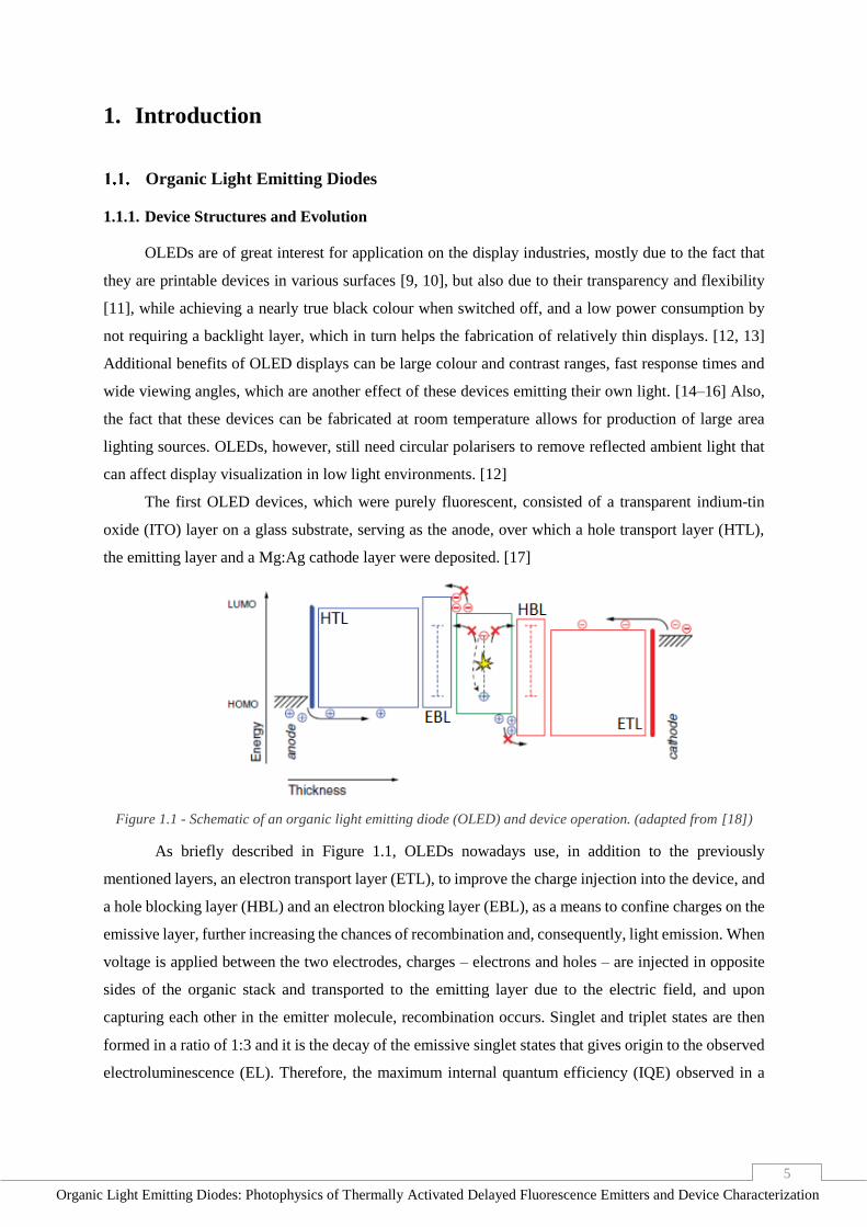
Figure 1.1 - Schematic of an organic light emitting diode (OLED) and device operation. (adapted from [18])
As briefly described in Figure 1.1, OLEDs nowadays use, in addition to the previously
mentioned layers, an electron transport layer (ETL), to improve the charge injection into the device, and
a hole blocking layer (HBL) and an electron blocking layer (EBL), as a means to confine charges on the
emissive layer, further increasing the chances of recombination and, consequently, light emission. When
voltage is applied between the two electrodes, charges – electrons and holes – are injected in opposite
sides of the organic stack and transported to the emitting layer due to the electric field, and upon
capturing each other in the emitter molecule, recombination occurs. Singlet and triplet states are then
formed in a ratio of 1:3 and it is the decay of the emissive singlet states that gives origin to the observed
electroluminescence (EL). Therefore, the maximum internal quantum efficiency (IQE) observed in a
6
Organic Light Emitting Diodes: Photophysics of Thermally Activated Delayed Fluorescence Emitters and Device Characterization
fluorescent OLED is 25%, consequently limiting the device’s external quantum efficiency (EQE), which
follows the equation:
EQE = ɣ 𝜂 𝜙𝑃𝐿 𝜒 (1)
where ɣ is the carrier balance factor, which can presently achieve near 100% through layer optimization,
η is the singlet yield, i.e. the yield of emissive excitons, which, for a pure fluorescent OLED, is set at
25% due to the singlet:triplet ratio of 1:3, ϕPL is the photoluminescence quantum yield, and χ is the
outcoupling efficiency, related to the amount of photons that can be extracted from the device, whose
achieved maximum is of around 25%. As such, new methods for increasing η and χ were required.
Since their first discovery, where an EQE of 1% was obtained, OLED devices have been
drastically improved, nowadays being able to reach an EQE over 20%. [19][8] Besides fluorescence,
the second generation of OLEDs relied on phosphorescence emission in order to address their
fluorescent counterparts’ main issue, the 1:3 singlet to triplet exciton ratio. This was achieved by
harvesting the dark triplet excitons by adding heavy metal complexes such as iridium to the emitter’s
molecular structure in order to facilitate ISC from singlets to emissive triplet states by exploiting spin-
orbit coupling (SOC), thus increasing phosphorescent emission. Despite being able to achieve 100%
internal quantum efficiencies through this method, similarly to most heavy metal complexes, iridium is
one of the most scarce naturally occurring elements on the planet, drastically increasing the cost of the
devices, and making them unreliable for large-scale production. [2, 20]
In 2012, a new generation of OLEDs emerged based on new method of harvesting triplet states,
allowing for their up-conversion into emissive singlet states without the use of heavy metals, generating
delayed fluorescence instead of phosphorescence. [14, 15] This method results in thermally activated
delayed fluorescence (TADF), explained in more detail further on this work.
1.1.2. Photoluminescence and Electroluminescence
The phenomenon of light emission, or luminescence, is caused by a transition of an electron from
an excited state to the ground state of a molecule, in which a photon is emitted. This transition is also
designated as radiative decay and can result in phosphorescence or fluorescence, based on whether the
electron decayed from a triplet or from a singlet excited state, respectively. [18, 21] For this phenomenon
to occur, however, molecules have to be electronically excited beforehand.
The excitation of organic molecules can be carried by two different ways: absorption of photons
– optically – or injection of electrons and holes – electrically –, the former being named
photoluminescence (PL) and the latter electroluminescence (EL). The resultant emission of an organic
molecule after excitation through either process is comparable. However, optical excitation allows for a
more detailed characterization of the excited states, as it has significantly higher time resolution, and so
it is preferred over electrical excitation for understanding and optimizing emitting structures.
Additionally, excitation by light is easily performed in liquid and solid samples whereas electron and
7
Organic Light Emitting Diodes: Photophysics of Thermally Activated Delayed Fluorescence Emitters and Device Characterization
hole injection is done in devices. As such, preliminary studies are usually conducted in solution and
solid thin films, before using a molecule as the emitting layer of an OLED device.
Molecular Photophysics
1.2.1. Atomic and Molecular Orbitals
Electrons in atomic orbitals can be described by four quantum numbers: the principal quantum
number (n), related to the energy of the orbital they are on; the orbital angular-momentum quantum
number (l), based on the shape of the atomic orbital and ranging from 0 to n-1 and represented by the
letters s, p, d and f, for values of 0, 1, 2 and 3, respectively; and the magnetic quantum number (ml),
which describes the orientation of the orbital in space and can have a value between -1 and 1, and in the
case of multiple-electron atoms, the spin quantum number (ms), which can either take values of -½ or
½, corresponding to the two directions in which an electron can spin, ↓ or ↑. [22]
Considering molecules, interactions occur between their constituent atomic orbitals consequently
generating molecular orbitals, from which the two frontier molecular orbitals define most of the
molecule electronic properties: a lower-energy bonding orbital and a higher-energy antibonding orbital
(as shown in Annex A). When the interaction is between p-orbitals, the resulting bonding and
antibonding orbitals are represented by π and π*, respectively. When the interacting atomic orbitals are
s-orbitals, the resulting orbitals are named σ, if bonding and σ*, if antibonding. Moreover, a nonbonding
orbital of energy higher than that of the bonding orbitals may exist, in only one of the atoms. Of all
molecular orbitals that are fully occupied by electrons, that which is the highest energetic is called
highest occupied molecular orbital (HOMO). Conversely, the lowest energy orbital that has no electrons
is called lowest unoccupied molecular orbital (LUMO), and so the lowest energy transition in an organic
molecule is between its HOMO and LUMO, typically known as the energy gap. [23]
Figure 1.2 - Representation of the ground and excited states of a diatomic organic molecule with two electrons,
showing their spin direction in each case on both the bonding (HOMO) and antibonding (LUMO) orbitals. [24]
When an atom or molecule is excited, the sum, S, of the previously mentioned spin quantum
number of the electrons in an orbital can specify the resultant excited state by allowing the determination
of its spin multiplicity, which is given by 2S+1. This means the spin multiplicity of a state can either
take the value of 1, describing a singlet state, or 3, referring to a triplet state. [1] For example, an organic
molecule’s ground state has two paired electrons of opposite spins in its highest occupied orbital
8
Organic Light Emitting Diodes: Photophysics of Thermally Activated Delayed Fluorescence Emitters and Device Characterization
(HOMO) so the spin multiplicity is 1 and, therefore, that state is a singlet (S0). The excited states,
however, have two possible spin configurations, as shown in Figure 1.2. In one of those configurations,
the electrons have a different spin, resulting in an excited singlet state (Sn, n based on the energy of the
orbital). The other possibility is that the electrons have the same spin direction and, as such, it is an
excited triplet state (Tn, n based on the energy of the orbital). The energy of a triplet state is always lower
than that of its corresponding singlet state because of the exchange interactions and coulomb repulsion
between its electron spins. [25, 26]
Because the HOMO and LUMO of most fluorescent molecules strongly overlap, the electrons of
a singlet excited state suffer Coulomb repulsion, thus increasing the energy of the state. On the other
hand, on a triplet excited state, this repulsion is not as intense, because the presence of two electrons
with the same quantum numbers is forbidden by the Pauli’s exclusion principle and, as a consequence,
its energy is lower than that of a singlet.
Figure 1.3 - Jablonski energy diagram with the main transitions starting from an electron absorption to its
decay back to the ground state. (adapted from [27])
As shown in Figure 1.3, when molecules are optically excited, a transition of an electron from its
ground state to a state of the same multiplicity is induced. From there, the electron will first relax from
its current vibrational state to the lowest vibrational state of that excited state by vibrational relaxation
(VR). If the electron is in S2 or higher, it will then be transferred to a lower energy state of the same
multiplicity until it reaches S1. Then, there are two possible outcomes, one of which consists on the
decay back to S0, which can occur through a non-radiative process (internal conversion) or through a
radiative process resulting in the emission of fluorescence. The other possibility is the transition to the
corresponding triplet state, T1, called intersystem crossing (ISC), which usually has a low probability of
occurring. From the T1 state, if the electron decays back to S0, there can be phosphorescence, though at
room temperature the probability is usually low. The wavelength (λ) of the emitted photon corresponds
to the energy gap (ΔE) between the state an electron decays from and the ground state, according to the
equation:
9
Organic Light Emitting Diodes: Photophysics of Thermally Activated Delayed Fluorescence Emitters and Device Characterization
𝛥𝐸 = hc
𝜆 (2)
where h is the Planck constant, 4.136×10⁻¹⁵ eV.s and c is the speed of light, 3×10⁸ m/s.
When molecules are excited by photons in order to emit light (photoluminescence), their excess
carriers normally generate singlet states. So, even though there is a chance of singlets becoming triplets
through ISC, radiative decays to the ground state have a significantly higher probability of occurring. In
electroluminescence, however, the excess carriers are obtained through electron and hole injection and,
statistically, there 25% of the generated excitons are singlet states and 75% are triplet states, implying
that only a third of charge recombination will result in emissive singlet states. [2][4]
1.2.2. Spin-Orbit Coupling
According to the spin selection rule, transitions between singlet and triplet states have a low
probability of occurring because they require a change in total spin multiplicity. [28] However, that is
only valid when not considering interactions between different electrons or nuclei in a molecule. When
those interactions are taken into account, the magnetic field that is consequence of the orbital motion of
an electron has influence over the magnetic field associated with the electron’s spin, promoting a spin-
orbit coupling (SOC) which allows for triplet character on the singlet states and vice-versa, increasing
the probability of ISC. This phenomenon occurs more frequently in molecules which have atoms of high
atomic mass, such as bromine, being also named heavy-atom effect. [29] The heavy-atom effect,
therefore, allows for either a higher rate of recycling between singlet and triplet excited states, while
also allowing for the possibility of increased phosphorescence by facilitating the pathways for electrons
to decay from triplets to the ground state.
Thermally Activated Delayed Fluorescence
TADF can be achieved by designing molecules with charge transfer (CT) states. In order to do
so, molecules are synthesised having an electron-donor and an electron-acceptor fragments of strong
charge transfer character, decreasing the spatial overlap of the HOMO and LUMO orbitals of the
molecule, consequently reducing the otherwise present Coulomb repulsion between electrons of a
singlet excited state, which in turn reduces the energy of that state. In the TADF mechanism, the lowest
excited triplet state (3LE), often localized in the electron donor or acceptor fragments, plays a
fundamental role in the intersystem crossing (ISC) mechanism, in the sense that, for TADF to occur,
CT→3LE and 3LE→CT transitions need to take place, with assistance from the environmental
temperature. [30] Hence, both processes are proportional to the energy gap between the involved states
(ΔEST), which should be minimized. [7]
TADF molecules may have three types of emission: prompt fluorescence (PF) lasting for
nanoseconds, delayed fluorescence (DF) with lifetimes of microseconds, and phosphorescence (PH) at
longer times, decaying milliseconds after excitation. PF corresponds to an S0 → Sn absorption and
10
Organic Light Emitting Diodes: Photophysics of Thermally Activated Delayed Fluorescence Emitters and Device Characterization
relaxation back to S0 with the emission of a photon of energy equal to the energy gap of those states.
DF, much like PF, first requires absorption to a Sn state, after which a transition to the S1 state through
VR and IC occurs, as well as a transition to the T1 state by ISC, sequentially, followed by a transition
back to S1 by thermally activated RISC where there will be an emissive decay to S0. Finally, PH occurs
when instead of RISC to S1, a relaxation occurs from the T1 state with a photon emission directly to the
ground state.
Figure 1.4 - Energy diagram representing the transitions involved in TADF emission. kRISC is the rate of reverse
intersystem crossing (T1 - S1 transitions), kf is the decay rate of singlet states to the ground state and kPH is the
rate of the radiative and non-radiative decays of triplet states to the ground state. (adapted from [2]).
The kinetics of TADF emitters have been thoroughly studied [2, 31], and can be better understood
with the energy diagram represented in Figure 1.4, where the PF component is neglected, as its lifetime
is much shorter. Knowing that, the following equations can be written to describe the evolution of the
singlet and triplet populations, following the initial decay of directly photo-excited singlet states and
taking into account only the singlet states generated by RISC. Such equations are useful to understand
how the lowest excited singlet and triplet state populations vary with time, following a pulse excitation,
showing the TADF component decays with the lifetime of the triplet state.
𝑑𝑆1
𝑑𝑡= −𝑘𝑓𝑆1 + 𝑘𝑅𝐼𝑆𝐶𝑇1 (3)
𝑑𝑇1
𝑑𝑡= −(𝑘𝑅𝐼𝑆𝐶 + 𝑘𝑃𝐻)𝑇1 (4)
when solved, the equations result in:
𝑇1(𝑡) = 𝑇1(0)𝑒−(𝑘𝑅𝐼𝑆𝐶+ 𝑘𝑃𝐻)𝑡 (5)
𝑆1(𝑡) =𝑘𝑅𝐼𝑆𝐶
𝑘𝑓 − (𝑘𝑅𝐼𝑆𝐶 + 𝑘𝑃𝐻) 𝑇1(0)𝑒−(𝑘𝑅𝐼𝑆𝐶+ 𝑘𝑃𝐻)𝑡 (6)
and, because TADF is fully dependent on the T1 state, which in turn relies on both kRISC and kPH, both
TADF and triplet state lifetimes (τ) can be written as:
𝜏𝑇𝐴𝐷𝐹 = 𝜏𝑇1=
1
𝑘𝑅𝐼𝑆𝐶 + 𝑘𝑃𝐻 (7)
11
Organic Light Emitting Diodes: Photophysics of Thermally Activated Delayed Fluorescence Emitters and Device Characterization
2. Materials and Methods
Molecular Structures
Figure 2.1 - Molecular structures of the molecules based on PTZ-DBTO2, compared throughout this work. a)
molecule 1, without bromine groups; b) molecule 2, with bromine groups. A corresponds to the acceptor
fragment (DBTO2), D to the donor fragment (PTZ), and D’’ to PTZ with bromine groups.
Molecules based on a phenothiazine (PTZ) electron-donor and a dibenzothiophene-S,S-dioxide
(DBTO2) electron-acceptor fragments, shown Figure 2.1, were studied throughout this work. Molecule
2 has an equivalent structure to that of molecule 1, but with the addition of bromine groups.
Characterization of Photophysical Properties
Absorption spectra was collected using a UV-Vis spectrophotometer (UV-3600, Shimadzu), with
a 0.5 nm step in solution.
Steady-state emission spectra were collected on a fluorimeter (Fluoromax, Jobin Yvon Horiba).
Excitation was kept at 320 nm on solvatochromism studies, and 355 nm, on temperature dependence
measurements. The spectra collected between 370 nm and 800 nm, with a 1 nm incremental step, and a
0.1 s integration time. Emission as a function of temperature was collected on another fluorimeter
(Fluorolog, Jobin Yvon Horiba), with the sample placed inside a cryostat (Janis Research Company,
Inc.), under vacuum. For temperature dependence, sample temperature was lowered from 320 K to 80
K, for solution samples, and increased from 80 K to 320 K, for solid samples, with a stabilization period
of 20 min at each temperature, so that the temperature would be uniform throughout the whole system.
Time-resolved measurements were conducted inside a similar cryostat. Excitation was achieved
with a pulsed neodymium-doped yttrium aluminium garnet (Nd:YAG) laser (SL-312, EKSPLA), and
emission collected through a spectrograph and imaged in intensified charge coupled device (iCCD)
camera (4 picos, Stanford Computer Optics). Liquid and solid samples were studied with excitation at
355 nm with a 10 Hz repetition rate, ensuring a maximum measurement window of 10 ms. For slower
decay samples, a nitrogen laser (MNL-100, LTB) (333 nm) was used as the excitation source with a
repetition rate of 2 Hz. The schematics of the time-resolved spectroscopy technique can be found in
Annex B.
a) b)
12
Organic Light Emitting Diodes: Photophysics of Thermally Activated Delayed Fluorescence Emitters and Device Characterization
Device Characterization
2.3.1. Steady-State Electroluminescence
For steady-state EL, the devices were placed in an integrating sphere, where voltage between 0 V
and 10 V was applied, at room temperature, generating curves of current density, external quantum
efficiency, luminous efficiency, device efficiency and brightness, as a function of voltage.
2.3.2. Transient Electroluminescence
Figure 2.2 - Simplified schematic of the assembled time-resolved electroluminescence spectroscopy technique,
for measurements of OLEDs transient EL.
For transient EL, a new technique was assembled, whose schematic is shown in Figure 2.2. This
setup was intended to allow for the study of transient electroluminescence, both as a function of applied
voltage and as a function of applied pulse duration. It contained a pulse generator, for device excitation,
a translation stage, to which a sample holder was attached, two lenses (one for light collection and the
second for light focusing), a magnifying 40× microscopic lens, and a variable gain high speed current
amplifier (DHPCA-100, Femto). Both the pulse generator and the amplifier’s output were connected to
an oscilloscope, of which the emission data could be extracted. All experiments were conducted at room
temperature, at the same pulse frequency of 10 Hz. Voltages above 12.5 V weren’t studied both because
practical applications for that range of voltage are scarce and because some test devices started showing
signs of damage.
To be certain that the response time of the used photodetector would be fast enough for DF to be
observable in the newly assembled technique, test measurements were conducted, with an excitation
pulse between 0 V and 5 V, with a duration of 100 µs and 800 µs.
13
Organic Light Emitting Diodes: Photophysics of Thermally Activated Delayed Fluorescence Emitters and Device Characterization
0 50 100 150 2000
1 E. Pulse
107 V/V
106 V/V
105 V/V
No
rmaliz
ed Inte
nsity (
V)
Time (s)
0 200 400 600 800 1000 12000
1 E. Pulse
107 V/V
106 V/V
105 V/V
No
rmaliz
ed Inte
nsity (
V)
Time (s)
Figure 2.3 – Normalized transient EL of an OLED, collected with different gains of the photodetector, with an
excitation pulse between 0 and 5 V and a duration of a) 100 μs; b) 800 μs.
In Figure 2.3 the normalized emissions of an OLED when 5 V are applied are shown, with pulse
durations of 100 μs and 800 μs, respectively, collected by the photodiode at different gains. Here, an
overlap between emissions is clear, meaning that the response of the system is independent of the
photodetector gain.
In addition to the previous study, it was necessary to guarantee that the RC constant of the overall
circuit wouldn’t also interfere with the measurements.
0 200 400 600 800 1000 1200 14000
1 E. Pulse
5 V
7.5 V
10 V
12.5 V
Norm
aliz
ed Inte
nsity (
V)
Time (s) Figure 2.4 - Transient EL of an OLED, excited with an electric pulse of 400 μs, at 5 V, 7.5 V, 10 V and 12.5 V.
As shown in Figure 2.4, a 2⨯2 mm2 OLED was tested, at a fixed pulse duration, at different
voltages, in order to determine the fastest response that would be viable to study. In these graphs, it is
possible to observe that, when 10 V or 12.5 V are applied on the OLED, it reaches its maximum emission
intensity in under 50 μs. Despite, possibly, not being the minimum response time of the devices, it is
safe to assume that measurements where emissions take longer than that, such as DF and
phosphorescence, are reliable for analysis.
a) b)
14
Organic Light Emitting Diodes: Photophysics of Thermally Activated Delayed Fluorescence Emitters and Device Characterization
Solution Preparation
For the absorption spectra, a solution of 1 mg/mL in the intended solvent was initially prepared.
To a few μL of that solution were added mL of solvent to decrease the concentration, having at least 5
solutions been prepared, all of lower concentration than the previous.
Regarding emission spectra, solutions were prepared to have an OD at 355 nm below 0.5. Further
preparation involved using a specially designed cuvette that is able to reach low temperatures up to 80
K, without breaking. This cuvette had a round section for freezing the solution and a tap to prevent
airflow. In order to remove the oxygen from the inside, a vacuum pump was attached to its opening and
the round section of the cuvette was dipped in liquid nitrogen, freezing the solution, after which the tap
was opened so that the pump would remove the air from inside. After a brief moment, the tap was closed
and the solution was left to thaw. Five freeze/thaw cycles were done for each solution.
Solid-State Sample Preparation
Quartz substrates were cleaned with dichloromethane, acetone and isopropyl alcohol, having been
dried in between each step.
To prepare solid-state films, the molecules were dissolved in toluene, with a concentration of 1
mg/mL. A commercial polymer (Zeonex) solution in toluene was prepared beforehand (176 mg/mL). A
final solution was then prepared at a 1:1 molecule to Zeonex ratio solutions. Then, 80 μL of this solution
were drop-cast on a quartz substrate and put under vacuum so that the solvent would evaporate. The
used substrate had been previously cleaned with nitric acid, deionized water, acetone, and isopropyl
alcohol and dried with nitrogen.
Device Fabrication
As in section 2.5, glass substrates were cleaned with acetone and isopropyl alcohol, but in an
ultrasound bath for 15 minutes in each, having been dried in between. The substrates were then cleaned
twice using a plasma system, for 3 minutes each process.
Two similar device structures were used on OLED fabrication for both steady-state and transient
EL measurements. Devices 1 (DEV1) have one of the structures presented in [30]: ITO/NPB (40
nm)/10% PTZ-DBTO2:CBP (20 nm)/TPBi (50 nm)/LiF (1 nm)/Al (100 nm). Devices 2 (DEV2) have
double the thickness of DEV1’s emissive layer, having 40 nm of 10% PTZ-DBTO2:CBP.
15
Organic Light Emitting Diodes: Photophysics of Thermally Activated Delayed Fluorescence Emitters and Device Characterization
3. Results and Discussion
Photophysics Studies
Since one of the objectives of this work was to study the impact of adding bromine to a TADF
emitter (molecule 1) based on a phenothiazine (PTZ) donor (D) and a dibenzothiophene-S,S-dioxide
(DBTO2) acceptor (A) - which has already shown outstanding results in OLED devices [30] -,
photophysics studies were conducted on a new molecule whose structure was similar to molecule 1, but
containing bromine groups on two ends of the donor fragment (molecule 2).
3.1.1. Absorption
Because the brominated donor fragment by itself was unavailable, in order to understand the
influence of heavy groups, studies were conducted on a donor fragment substituted with methyl groups
instead of bromine atoms (D’), which despite being lighter, allow to follow the impact of these
substitution on the photophysics of this molecule. The same studies were performed for the acceptor
fragment, shown in Annex C
250 300 3500
1
2
3
4
5 Molecule
D
D'
x 1
0-4 (
L m
ol -
1 c
m-1)
Wavelength (nm)
Figure 3.1 - Absorption spectra of D fragment and its analogue which has methyl groups, normalized by Ɛ.
Figure 3.1 represents the extinction coefficient (calculation method shown in Annex D) of the
unsubstituted and methyl substituted analogues of Phenothiazine, revealing the impact of the substituent
group in the photophysical properties of this molecule. Firstly, an increase on the extinction coefficient
of the substitute D molecule is observed. Secondly, there is a clear red-shift of the electronic transition
peaks, relatively to the unsubstituted analogue. Based on this information, we can assume that the
addition of bromine groups, which are heavier than the methyl chains, would result in the same
variations in the spectrum, but at a higher degree.
16
Organic Light Emitting Diodes: Photophysics of Thermally Activated Delayed Fluorescence Emitters and Device Characterization
250 300 350 4000
1
2
3
4
5
Molecule
1
2
D
A
x 1
0-4 (
L m
ol -
1 c
m-1)
Wavelength (nm)
Figure 3.2 – Absorption spectra of both molecule 1, molecule 2 and A and D fragments, normalized by Ɛ.
Table 3.1 - Extinction coefficient and absorption peaks of molecules 1 and 2, normalized by Ɛ.
Figure 3.2 shows that the absorption of molecule 2 is clearly the sum of both the D and A
fragments. While the A fragment’s contribution is at lower wavelengths on both molecules, the
previously mentioned red-shift caused by the presence of bromine atoms is noticeable, having the D
fragment’s contribution peak shifted approximately 15 nm from molecule 1’s. In addition, the figure
portraits a considerable change in the absorption of molecule 2 with the addition of bromine groups, not
only in its intensity, which is higher, but also in its overall shape, revealing a greater contribution from
D in that molecule than in molecule 1. Table 3.1 summarizes the values of Ɛ and the maximum
absorption peaks of each molecule of the D-A molecules.
3.1.2. Triplets and Charge-Transfer States
Since the TADF mechanism is based on the ISC between the CT and 3LE states, it was necessary
to verify the presence of a CT state in molecule 2 by observing the molecule’s emission in solvents with
different polarities. In higher polarity environments, should there be a CT state, a molecule’s
fluorescence would be red-shifted because these states have a high dipolar moment themselves, making
them environment polarity-sensitive. This shift is a consequence of the molecule becoming in a more
relaxed conformation, decreasing the energy gap (∆E) between the CT states and S0, causing the
emission from a decay from the CT to be at a longer wavelength. These states should be inexistent in
the separated acceptor and donor fragments since CT states are only observed when both a charge donor
and a charge acceptor are present in the same molecule or in the same solution for intramolecular or
intermolecular CT, respectively.
Molecule Ɛ (L mol-1 cm-1) Max. Absorption Peak (nm)
1 6432.97 245
2 48768.64 265
17
Organic Light Emitting Diodes: Photophysics of Thermally Activated Delayed Fluorescence Emitters and Device Characterization
400 450 500 550 6000
1
No
rmaliz
ed Inte
nsity (
a.u
.)
Wavelength (nm)
Solvent
ACN
DCM
2-MeTHF
300 350 400 4500
1
No
rmaliz
ed Inte
nsity (
a.u
.)
Wavelength (nm)
Solvent
ACN
DCM
Figure 3.3 - Emission spectra, in different polarity solvents, of a) D fragment; b) A fragment.
Figure 3.3 a) reveals little to no changes in the emission spectrum of DBTO2 in different polarity
solvents. The same is shown in Figure 3.3 b) for PTZ, therefore confirming the absence of CT states in
both these molecules.
400 500 600 700 8000
1
DCM
2-MeTHF
Toluene
MCH
No
rmaliz
ed Inte
nsity
(a.u
.)
Wavelength (nm)
400 450 500 550 600 650 700 750 8000
1
DCM
Toluene
2-MeTHF
No
rmaliz
ed Inte
nsity (
a.u
.)
Wavelength (nm)
Figure 3.4 - Normalized emission of a) molecule 1; b) molecule 2; in different polarity solvents, excited with a
wavelength of 320 nm.
Figure 3.4 a) shows evidence of the existence of an intramolecular CT state in molecule 1, since
the prepared solutions contained only one of the molecules (1 or 2) and its emission is clearly shifting
towards red in higher polarity environments. The same can be verified for molecule 2, in Figure 3.4 b).
Noticeably, molecule 1 has two significant emission peaks, which are attributed to the presence of two
different conformers of the same molecule in those solutions. [30] However, looking at molecule 2’s
emission there is only one strong emission peak, which is blue-shifted comparing to molecule 1’s more
intense peak. The disappearance of one of the peaks in molecule 2 strongly implies that the presence of
bromine groups considerably diminishes the molecular rotations that cause different conformers to
surge. No emission of molecule 2 in MCH was collected because of the low solubility of the molecule
in that solvent.
Knowing that oxygen’s ground state is a triplet, its interactions with a molecule’s triplet excited
states results in a drastic quenching of the latter. As such, the triplet contribution to the overall emission
a)
a) b)
b)
18
Organic Light Emitting Diodes: Photophysics of Thermally Activated Delayed Fluorescence Emitters and Device Characterization
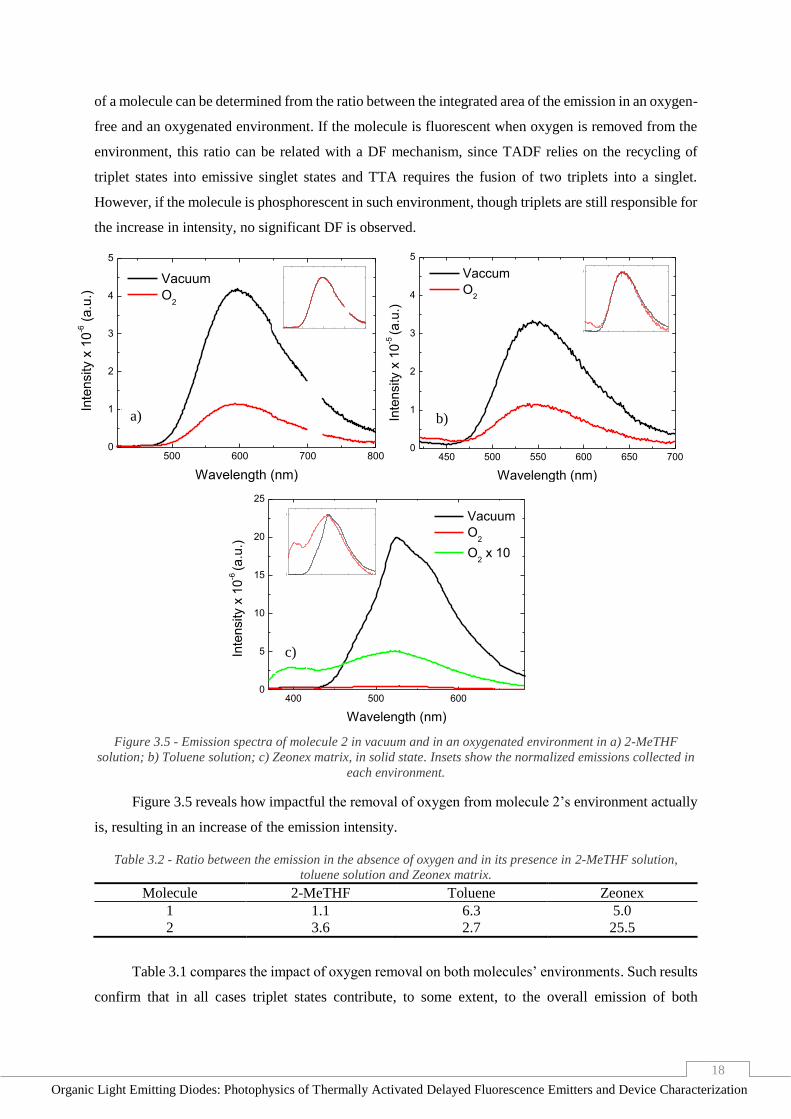
of a molecule can be determined from the ratio between the integrated area of the emission in an oxygen-
free and an oxygenated environment. If the molecule is fluorescent when oxygen is removed from the
environment, this ratio can be related with a DF mechanism, since TADF relies on the recycling of
triplet states into emissive singlet states and TTA requires the fusion of two triplets into a singlet.
However, if the molecule is phosphorescent in such environment, though triplets are still responsible for
the increase in intensity, no significant DF is observed.
500 600 700 8000
1
2
3
4
5
500 600 700 8000
1N
orm
aliz
ed Inte
nsity (
a.u
.)
Wavelength (nm)
Inte
nsity x
10
-6 (
a.u
.)
Wavelength (nm)
Vacuum
O2
450 500 550 600 650 7000
1
2
3
4
5
500 600 7000
1
Norm
aliz
ed Inte
nsi
ty (
a.u
.)
Inte
nsity x
10
-5 (a
.u.)
Wavelength (nm)
Vaccum
O2
400 500 6000
5
10
15
20
25
400 500 600 7000
1
Norm
aliz
ed Inte
nsity (
a.u
.)
Vacuum
O2
O2 x 10
Inte
nsity x
10
-6 (a
.u.)
Wavelength (nm)
Figure 3.5 - Emission spectra of molecule 2 in vacuum and in an oxygenated environment in a) 2-MeTHF
solution; b) Toluene solution; c) Zeonex matrix, in solid state. Insets show the normalized emissions collected in
each environment.
Figure 3.5 reveals how impactful the removal of oxygen from molecule 2’s environment actually
is, resulting in an increase of the emission intensity.
Table 3.2 - Ratio between the emission in the absence of oxygen and in its presence in 2-MeTHF solution,
toluene solution and Zeonex matrix.
Molecule 2-MeTHF Toluene Zeonex
1 1.1 6.3 5.0
2 3.6 2.7 25.5
Table 3.1 compares the impact of oxygen removal on both molecules’ environments. Such results
confirm that in all cases triplet states contribute, to some extent, to the overall emission of both
a) b)
c)
19
Organic Light Emitting Diodes: Photophysics of Thermally Activated Delayed Fluorescence Emitters and Device Characterization
molecules. The insets of the figures are evidence that the emission in vacuum and in presence of oxygen
are originated from the same molecular state.
In solution, the Gaussian shape of the emission implies that fluorescence is the dominant
deactivation pathway, and the fact that it increases in the absence of oxygen indicates that triplet states
contribute significantly to the overall fluorescence emission in the form of delayed fluorescence.
However, in solid-state, the shape of the emission is no longer according to a Gaussian distribution,
revealing that phosphorescence is stronger in this scenario, where it’s observable that, by removing the
triplet states’ main quencher, transitions from 3LE to the ground state occur with ease, suggesting that
the presence of the bromine groups on the molecule’s structure establishes a heavy atom effect, not seen
in both solutions due to their vibronic constraints being considerably less significant.
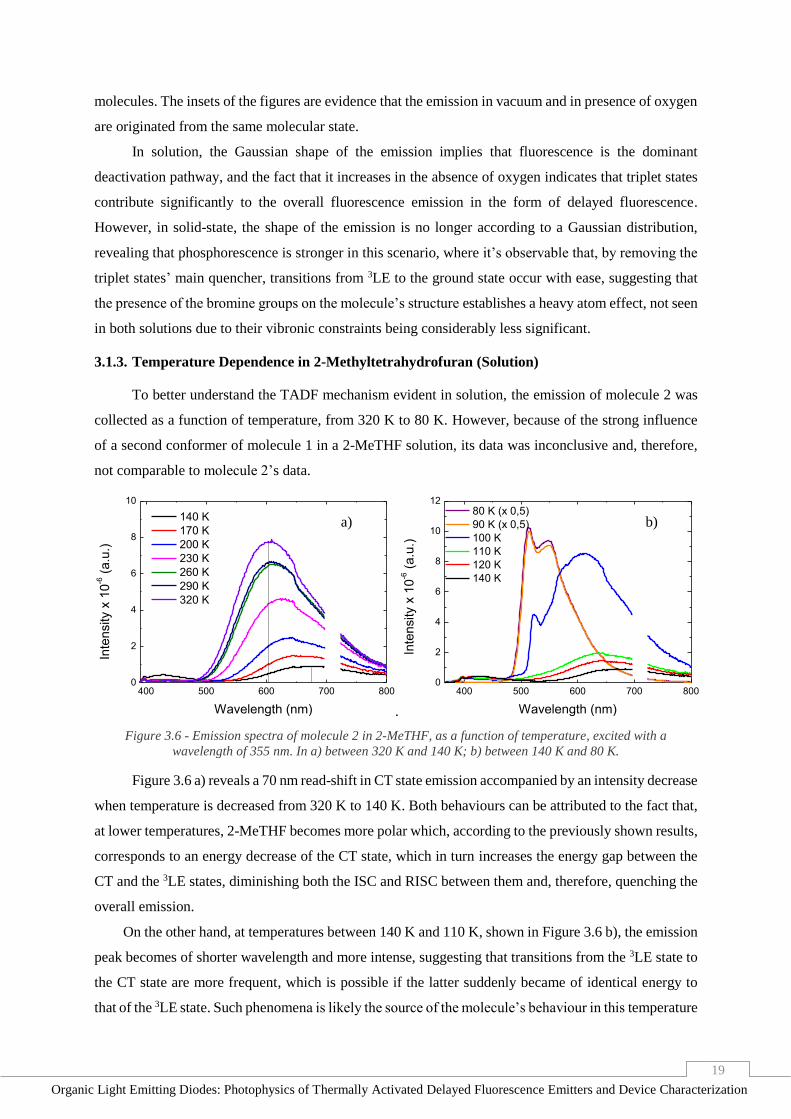
3.1.3. Temperature Dependence in 2-Methyltetrahydrofuran (Solution)
To better understand the TADF mechanism evident in solution, the emission of molecule 2 was
collected as a function of temperature, from 320 K to 80 K. However, because of the strong influence
of a second conformer of molecule 1 in a 2-MeTHF solution, its data was inconclusive and, therefore,
not comparable to molecule 2’s data.
400 500 600 700 8000
2
4
6
8
10
140 K
170 K
200 K
230 K
260 K
290 K
320 K
Inte
nsity x
10
-6 (
a.u
.)
Wavelength (nm) .
400 500 600 700 8000
2
4
6
8
10
12
Inte
nsity x
10
-6 (
a.u
.)
Wavelength (nm)
80 K (x 0,5)
90 K (x 0,5)
100 K
110 K
120 K
140 K
Figure 3.6 - Emission spectra of molecule 2 in 2-MeTHF, as a function of temperature, excited with a
wavelength of 355 nm. In a) between 320 K and 140 K; b) between 140 K and 80 K.
Figure 3.6 a) reveals a 70 nm read-shift in CT state emission accompanied by an intensity decrease
when temperature is decreased from 320 K to 140 K. Both behaviours can be attributed to the fact that,
at lower temperatures, 2-MeTHF becomes more polar which, according to the previously shown results,
corresponds to an energy decrease of the CT state, which in turn increases the energy gap between the
CT and the 3LE states, diminishing both the ISC and RISC between them and, therefore, quenching the
overall emission.
On the other hand, at temperatures between 140 K and 110 K, shown in Figure 3.6 b), the emission
peak becomes of shorter wavelength and more intense, suggesting that transitions from the 3LE state to
the CT state are more frequent, which is possible if the latter suddenly became of identical energy to
that of the 3LE state. Such phenomena is likely the source of the molecule’s behaviour in this temperature
a) b)
20
Organic Light Emitting Diodes: Photophysics of Thermally Activated Delayed Fluorescence Emitters and Device Characterization
range, since at temperatures lower than 140 K, the solvent starts to freeze, which is known to make it
significantly less polar, therefore causing the increasing of the energy of the CT state, as previously
shown in chapter 3.1.3. This change in energies could also justify the dominance of phosphorescence
on the emission below 100 K simply because, at that point, the CT state can already be more energetic
than the 3LE state and, because there is no thermal energy to promote TADF.
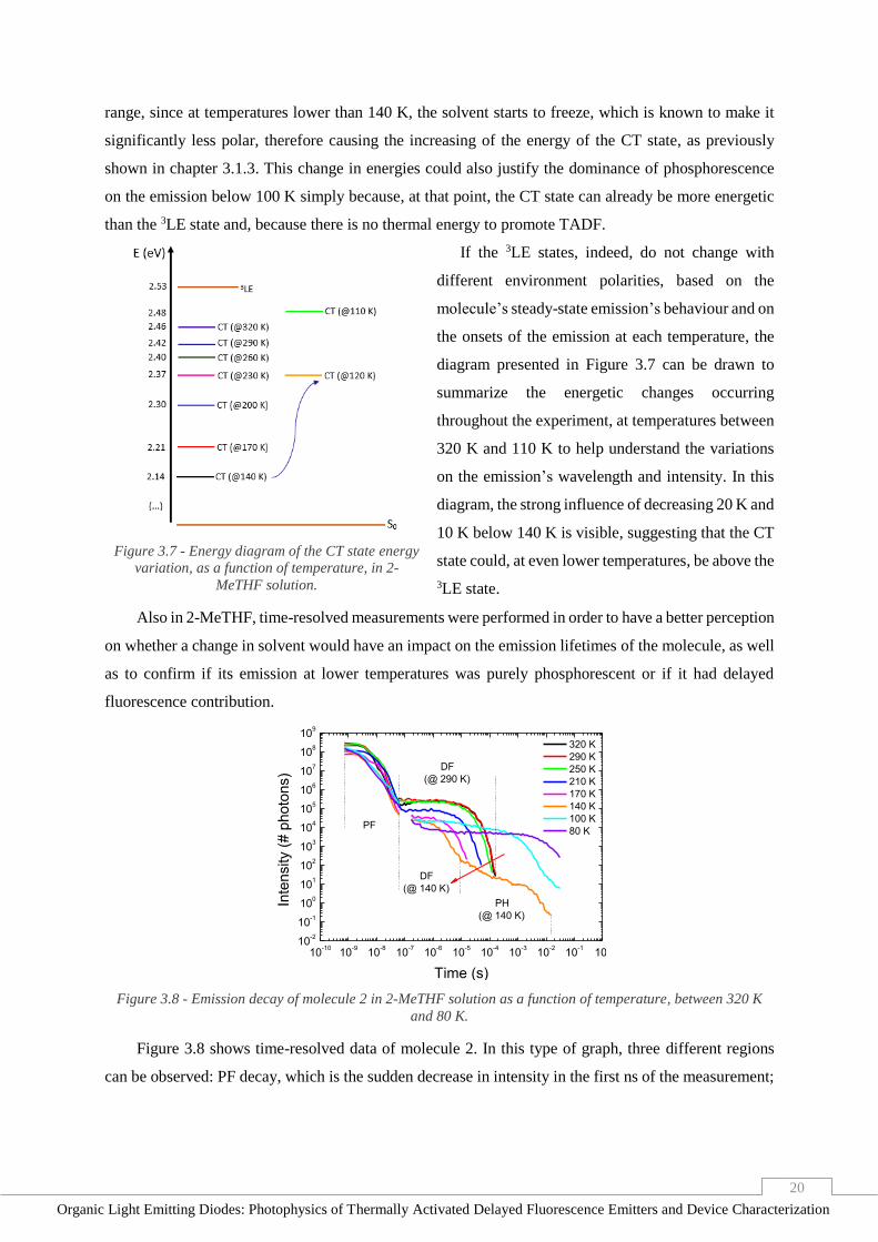
Figure 3.7 - Energy diagram of the CT state energy
variation, as a function of temperature, in 2-
MeTHF solution.
If the 3LE states, indeed, do not change with
different environment polarities, based on the
molecule’s steady-state emission’s behaviour and on
the onsets of the emission at each temperature, the
diagram presented in Figure 3.7 can be drawn to
summarize the energetic changes occurring
throughout the experiment, at temperatures between
320 K and 110 K to help understand the variations
on the emission’s wavelength and intensity. In this
diagram, the strong influence of decreasing 20 K and
10 K below 140 K is visible, suggesting that the CT
state could, at even lower temperatures, be above the
3LE state.
Also in 2-MeTHF, time-resolved measurements were performed in order to have a better perception
on whether a change in solvent would have an impact on the emission lifetimes of the molecule, as well
as to confirm if its emission at lower temperatures was purely phosphorescent or if it had delayed
fluorescence contribution.
10-10
10-9
10-8
10-7
10-6
10-5
10-4
10-3
10-2
10-1
100
10-2
10-1
100
101
102
103
104
105
106
107
108
109
DF
(@ 140 K)
320 K
290 K
250 K
210 K
170 K
140 K
100 K
80 K
Inte
nsity (
# p
hoto
ns)
Time (s)
PF
PH
(@ 140 K)
DF
(@ 290 K)
Figure 3.8 - Emission decay of molecule 2 in 2-MeTHF solution as a function of temperature, between 320 K
and 80 K.
Figure 3.8 shows time-resolved data of molecule 2. In this type of graph, three different regions
can be observed: PF decay, which is the sudden decrease in intensity in the first ns of the measurement;
21
Organic Light Emitting Diodes: Photophysics of Thermally Activated Delayed Fluorescence Emitters and Device Characterization
DF decay, the second decrease of intensity at the highest temperatures in the time scale of the μs; and
the PH decay that corresponds to the longest intensity decrease, only observable at lower temperatures.
At first glance, the information portrayed on the figure is according to the steady-state data,
revealing a decrease in emission intensity when the temperature lowers from 320 K to 140 K, below
which it suddenly becomes more intense. However, a strange behaviour between 320 K and 140 K is
also registered, as the lifetime of the DF is decreasing from about 200 µs to 30 µs with decreasing
temperature. Knowing that at lower temperatures kRISC is also lower due to less thermal energy and
vibronic constraints, such behaviour is surprising because, according to equation 6, in those
circumstances, τTADF should increase. This decrease has never been registered before, suggesting a
mixing between the 3LE and the CT states. At higher temperatures, such mixing is strong, due to their
vibronic coupling and to their relatively small energy gap. When temperature decreases there are less
vibrations on the environment and, as previously shown, the energy gap increases, weakening the mixing
of the states. If that is, indeed, the case, then the properties of 3LE are changing, and the trend of longer
lifetimes at lower temperatures is not observed. Then, at 100 K, when the solvent starts to freeze and the
energy gap shortens, the mixing gets stronger again, DF contribution increases and so does its lifetime.
At 80 K, TADF is extremely unlikely, turning the molecule into a phosphorescent emitter, with a lifetime
of around 1 s, which is considerably long.
3.1.4. Temperature Dependence in Toluene (Solution)
Toluene freezes at around 180 K and its glass properties allow for it to crack easily and,
eventually, shatter. This response limits the temperature range in which the solution could be studied
safely, as the shattering of the glass could potentially break the cuvette it was on. As a precaution, all
temperature dependence measurements involving toluene were conducted from 320 K to 180 K.
Using this solvent, molecule 1’s second conformer isn’t as impactful as in the previous case and
its data can be used to try to understand the influence of the bromine groups.
400 450 500 550 600 650 700 7500
6
12
18
Inte
nsity x
10
-6 (
a.u
.)
Wavelength (nm)
320 K
310 K
270 K
250 K
230 K
210 K
200 K
190 K
180 K
400 500 600 7000
2
4
6
8
Inte
nsity x
10
-6 (
a.u
.)
Wavelength (nm)
320 K
290 K
260 K
240 K
220 K
200 K
180 K
Figure 3.9 - Emission spectra, as a function of temperature, in a toluene solution, of a) molecule 1; [32] b)
molecule 2.
a) b)
22
Organic Light Emitting Diodes: Photophysics of Thermally Activated Delayed Fluorescence Emitters and Device Characterization
Figure 3.9 portraits the same type of behaviour of both molecules emission shift, as seen in
molecule 2’s solution in 2-MeTHF, where the decrease of temperature translates into an increase of the
emission peak’s wavelength. However, in this case, the emission intensity doesn’t vary consistently,
increasing and decreasing between some of the temperatures, opposite of its behaviour in the previous
solvent, in which temperature would only decrease with decreasing temperatures. Such variations could
be attributed to the temperature not being given enough time to stabilize, but the fact that both molecules
show the same behaviour, those variations are most likely related the solvent. This could be because of
toluene’s lower polarity, which causes the CT state of the molecules to be of higher energy at room
temperature, changing the way the transitions compete amongst each other when compared to 2-
MeTHF.
Figure 3.10 - Energy diagram of the CT state
variation as a function of temperature in
toluene solution.
By analysing the onsets of each emission peak, and
assuming that the 3LE energy didn’t actually change in
this solvent, nor changes at different temperatures, the
diagram in Figure 3.10 can be drawn, showing that, in
toluene, the CT state is of higher energy than 3LE for
temperatures between 320 K and 230 K and of lower
energy, below that temperature. Additionally, between
320 K and 260 K the onsets of the emissions appear to be
equal. The registered intensity increase when decreasing
temperature from 320 K to 290 K might be related to the
fact that, the higher the temperature, the more vibrations
on the system, which in consequence can result in an
increase of non-radiative decays, quenching the emission.
Such vibrations, although still allowed at 290 K, would not quench the emission as much. By proceeding
with the decrease of temperature, the energy gap between 3LE and CT states would keep increasing,
lowering the kRISC constant and the associated DF. Although the temperature restrictions on this solvent
didn’t allow for a clear observation of a phosphorescent emission, it can already be existent at 200 K
and 180 K, justifying the intensity increase of the emissions at those temperatures.
23
Organic Light Emitting Diodes: Photophysics of Thermally Activated Delayed Fluorescence Emitters and Device Characterization
10-9
10-8
10-7
10-6
10-5
10-4
10-3
10-1
100
101
102
103
104
105
106
107
108
300K
250K
200K
Inte
nsity (
# p
hoto
ns)
Time (s)10
-910
-810
-710
-610
-510
-410
-310
-1
100
101
102
103
104
105
106
107
108
Inte
nsity (
# p
hoto
ns)
180 K
200 K
230 K
260 K
290 K
320 K
Time (s)
Figure 3.11 - Emission intensity, as a function of time and temperature, in toluene solution, of a) molecule 1,
between 300 K and 200 K; [32] b) 2, between 320 K and 180 K.
The absolute emission intensity of the two samples can’t be compared because it’s not only
affected by each solution’s concentration, but also by the cuvette’s relative position to the excitation
source and to the iCCD camera. However, the lifetimes are not affected by the collection geometry and
concentration. and so, they can be compared. Therefore, we can rely on the analysis of transient data to
highlight possible differences in the ISC mechanism in both molecules. When comparing both
molecules’ lifetime, in Figure 3.11, a noticeable change in the emission decays is observed. Primarily,
PF decays ten times slower on the non-brominated molecule. Also, while molecule 1’s emission is
continuous, in the sense that after PF comes DF immediately after, in molecule 2 that behaviour isn’t
observed, registering a time gap close to 10 μs between both types of fluorescence. Looking at the DF
lifetimes specifically, that emission in molecule 2 is one order of magnitude longer than that of molecule
1, suggesting a prolonged recycling of charges between the 3LE and CT states most likely related to a
heavy-atom effect caused by the presence of the bromine groups.
Figure 3.11 b) reveals that, between 320 K and 260 K, the lifetimes of the emissions of molecule
2 in toluene don’t seem to change and at 230 K, it becomes longer, as it did in the previous solvent.
From 200 K to 180 K, however, although of relatively low intensity and very brief, some
phosphorescence is observed, explaining the sudden increase in lifetimes and the intensity increase at
these temperatures, registered in steady-state emission.
3.1.5. Temperature Dependence in Zeonex (Solid Film)
As seen in section 3.1.2, in solid-state, the absence of surrounding oxygen significantly increases
the molecule’s emission more than in any of the other scenarios, which is due to its emission being
primarily phosphorescence. As such, this molecule can be categorized as a RTP emitter when in solid
state.
a) b)
24
Organic Light Emitting Diodes: Photophysics of Thermally Activated Delayed Fluorescence Emitters and Device Characterization
400 450 500 550 6000.0
0.3
0.6
0.9
1.2
1.5
Inte
nsity x
10
-6 (
a.u
.)
Wavelength (nm)
180 K
200 K
220 K
240 K
260 K
280 K
300 K
320 K
400 450 500 550 6000.0
0.4
0.8
1.2
Inte
nsity x
10
-6 (
a.u
.)
Wavelength (nm)
80 K
100 K
120 K
140 K
150 K
160 K
180 K
400 500 600 7000
5
10
15
20
25
80 K
100 K
120 K
140 K
160 K
180 K
200 K
220 K
240 K
260 K
280 K
290 K
300 K
320 K
Inte
nsity x
10
-6 (
a.u
.)
Wavelength (nm) Figure 3.12 - Emission spectra, as a function of temperature in a Zeonex matrix, of molecule a) 1, between 320
K and 180 K; b) 1, between 180 K and 80 K; c) 2, between 320 K and 80 K. Results from a) and b) were adapted
from [30].
Figure 3.12 a) and b) show the emission of molecule 1 in solid-state, where fluorescence is the
dominant emitting process from 320 K to 180 K. Interestingly, the steady-state emission of molecule 2
as a function of temperature, represented in Figure 3.12 c), reveals that in solid-state, throughout the
whole temperature range, its emission remains practically unchanged and its shape is that of
phosphorescence. This fact advocates that the mechanism involved in the emission doesn’t rely on
temperature to work and, therefore, doesn’t greatly depend on transitions from a CT state to the 3LE
state. Moreover, it strongly suggests that the presence of bromine, in solid-state, promotes radiative
transitions from the 3LE to the ground state assisted by SOC, also facilitated by the low possibility of
vibrations that weaken non-radiative decays.
In both cases, the emission doesn’t suffer any shift with temperature variations, as opposed to
what was observed in solution. This is justified by the fact that the polarity of Zeonex is low and, as
such, temperature won’t affect it much.
a) b)
c)
25
Organic Light Emitting Diodes: Photophysics of Thermally Activated Delayed Fluorescence Emitters and Device Characterization
10-8
10-7
10-6
10-5
10-4
10-3
10-2
10-1
100
10-1
101
103
105
107
109
1011
105 K
190 K
210 K
230 K
250 K
270 K
Inte
nsity (
# p
hoto
ns)
Time (s)
10-9
10-8
10-7
10-6
10-5
10-4
10-3
10-2
10-1
100
10-1
101
103
105
107
109
1011
Inte
nsity (
# p
hoto
ns)
80 K
120 K
170 K
210 K
250 K
290 K
320 K
Time (s)
Figure 3.13 - Emission intensity, as a function of time and temperature, in a Zeonex matrix, of molecules a) 1,
between 270 K and 105 K; [32] b) 2, between 320 K and 80 K.
Figure 3.13 a) shows the lifetime decays of molecule 1. Despite not being seen in steady-state,
through Figure 3.13 b), the existence of DF on the overall emission of molecule 2 is perceptible.
However, while the DF of molecule 1 seemingly stops 0.2 ms after excitation, molecule 2’s DF lasts
from 500 ns to 1 ms, between 250 K and 290 K. Furthermore, the figures propose that, in the solid state,
both these molecules’ emission behave in accordance with equation 7. Nonetheless, this information
doesn’t refute the possibility of a mixing between 3LE and CT states suggested in section 3.1.3 because,
in that section, the cause for the unusual lifetime behaviour at lower temperatures was attributed to the
change of the CT state’s energy as a consequence of the solvent’s polarity variations with temperature,
which, as previously stated, are not seen on this experiment since the Zeonex matrix used does not suffer
significant polarity variations with temperature.
450 500 550 600 6500
1
No
rmaliz
ed A
rea (
a.u
.)
Wavelength (nm)
Figure 3.14 - Photoluminescence spectra of molecule 2, in a Zeonex matrix, between 1.8 μs and 177.8 μs after
excitation, at 80 K.
Interestingly, looking at the emission changes at 80 K, presented in Figure 3.14, it is evident that
the right-most part of the fluorescence starts to decrease with time, followed by an emission increase
between 450 and 500 nm, giving the rise of phosphorescence.
a) b)
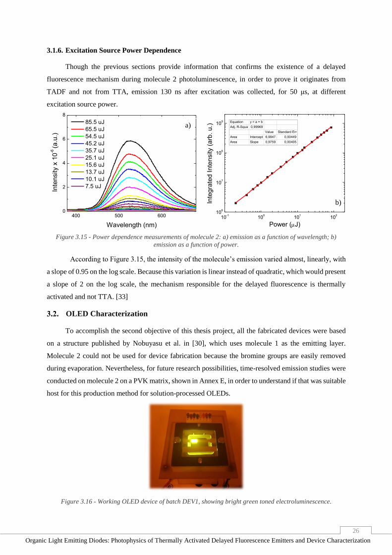
26
Organic Light Emitting Diodes: Photophysics of Thermally Activated Delayed Fluorescence Emitters and Device Characterization
3.1.6. Excitation Source Power Dependence
Though the previous sections provide information that confirms the existence of a delayed
fluorescence mechanism during molecule 2 photoluminescence, in order to prove it originates from
TADF and not from TTA, emission 130 ns after excitation was collected, for 50 μs, at different
excitation source power.
400 500 6000
2
4
6
8
85.5 uJ
65.5 uJ
54.5 uJ
45.2 uJ
35.7 uJ
25.1 uJ
15.6 uJ
13.7 uJ
10.1 uJ
7.5 uJ
Inte
nsity x
10
-6 (a
.u.)
Wavelength (nm)
10-1
100
101
102
106
107
108
109
Inte
gra
ted Inte
nsity (
arb
. u.)
Power (J)
Equation y = a + b
Adj. R-Squa 0,99969
Value Standard Err
Area Intercept 6,9947 0,00449
Area Slope 0,9759 0,00405
Figure 3.15 - Power dependence measurements of molecule 2: a) emission as a function of wavelength; b)
emission as a function of power.
According to Figure 3.15, the intensity of the molecule’s emission varied almost, linearly, with
a slope of 0.95 on the log scale. Because this variation is linear instead of quadratic, which would present
a slope of 2 on the log scale, the mechanism responsible for the delayed fluorescence is thermally
activated and not TTA. [33]
OLED Characterization
To accomplish the second objective of this thesis project, all the fabricated devices were based
on a structure published by Nobuyasu et al. in [30], which uses molecule 1 as the emitting layer.
Molecule 2 could not be used for device fabrication because the bromine groups are easily removed
during evaporation. Nevertheless, for future research possibilities, time-resolved emission studies were
conducted on molecule 2 on a PVK matrix, shown in Annex E, in order to understand if that was suitable
host for this production method for solution-processed OLEDs.
Figure 3.16 - Working OLED device of batch DEV1, showing bright green toned electroluminescence.
a)
b)
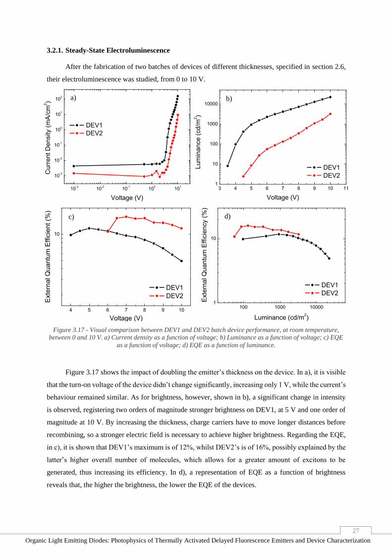
27
Organic Light Emitting Diodes: Photophysics of Thermally Activated Delayed Fluorescence Emitters and Device Characterization
3.2.1. Steady-State Electroluminescence
After the fabrication of two batches of devices of different thicknesses, specified in section 2.6,
their electroluminescence was studied, from 0 to 10 V.
10-3
10-2
10-1
100
101
10-3
10-2
10-1
100
101
102
Cu
rrent D
ensity (
mA
/cm
2)
Voltage (V)
DEV1
DEV2
3 4 5 6 7 8 9 10 111
10
100
1000
10000
DEV1
DEV2
Lum
inance (
cd/m
2)
Voltage (V)
4 5 6 7 8 9 10
10
DEV1
DEV2
Exte
rnal Q
uantu
m E
ffic
ient (%
)
Voltage (V)
100 1000 100001
10
DEV1
DEV2
E
xte
rnal Q
uantu
m E
ffic
iency (
%)
Luminance (cd/m2)
Figure 3.17 - Visual comparison between DEV1 and DEV2 batch device performance, at room temperature,
between 0 and 10 V. a) Current density as a function of voltage; b) Luminance as a function of voltage; c) EQE
as a function of voltage; d) EQE as a function of luminance.
Figure 3.17 shows the impact of doubling the emitter’s thickness on the device. In a), it is visible
that the turn-on voltage of the device didn’t change significantly, increasing only 1 V, while the current’s
behaviour remained similar. As for brightness, however, shown in b), a significant change in intensity
is observed, registering two orders of magnitude stronger brightness on DEV1, at 5 V and one order of
magnitude at 10 V. By increasing the thickness, charge carriers have to move longer distances before
recombining, so a stronger electric field is necessary to achieve higher brightness. Regarding the EQE,
in c), it is shown that DEV1’s maximum is of 12%, whilst DEV2’s is of 16%, possibly explained by the
latter’s higher overall number of molecules, which allows for a greater amount of excitons to be
generated, thus increasing its efficiency. In d), a representation of EQE as a function of brightness
reveals that, the higher the brightness, the lower the EQE of the devices.
c) d)
b) a)
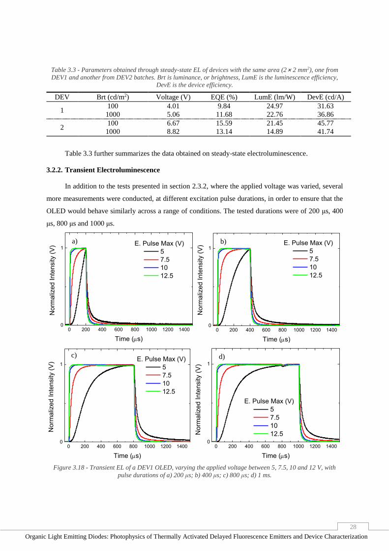
28
Organic Light Emitting Diodes: Photophysics of Thermally Activated Delayed Fluorescence Emitters and Device Characterization
Table 3.3 - Parameters obtained through steady-state EL of devices with the same area (2⨯ 2 mm2), one from
DEV1 and another from DEV2 batches. Brt is luminance, or brightness, LumE is the luminescence efficiency,
DevE is the device efficiency.
Table 3.3 further summarizes the data obtained on steady-state electroluminescence.
3.2.2. Transient Electroluminescence
In addition to the tests presented in section 2.3.2, where the applied voltage was varied, several
more measurements were conducted, at different excitation pulse durations, in order to ensure that the
OLED would behave similarly across a range of conditions. The tested durations were of 200 μs, 400
μs, 800 μs and 1000 μs.
0 200 400 600 800 1000 1200 14000
1E. Pulse Max (V)
5
7.5
10
12.5
Norm
aliz
ed Inte
nsity (
V)
Time (s)
0 200 400 600 800 1000 1200 14000
1E. Pulse Max (V)
5
7.5
10
12.5
Norm
aliz
ed Inte
nsity (
V)
Time (s)
0 200 400 600 800 1000 1200 14000
1E. Pulse Max (V)
5
7.5
10
12.5
No
rmaliz
ed Inte
nsity (
V)
Time (s)
0 200 400 600 800 1000 1200 14000
1
E. Pulse Max (V)
5
7.5
10
12.5Norm
aliz
ed Inte
nsity (
V)
Time (s)
Figure 3.18 - Transient EL of a DEV1 OLED, varying the applied voltage between 5, 7.5, 10 and 12 V, with
pulse durations of a) 200 μs; b) 400 μs; c) 800 μs; d) 1 ms.
DEV Brt (cd/m2) Voltage (V) EQE (%) LumE (lm/W) DevE (cd/A)
1 100 4.01 9.84 24.97 31.63
1000 5.06 11.68 22.76 36.86
2 100 6.67 15.59 21.45 45.77
1000 8.82 13.14 14.89 41.74
a) b)
c) d)
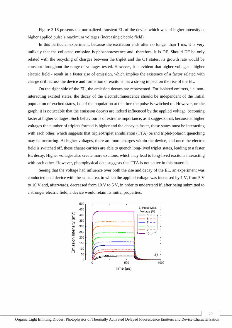
29
Organic Light Emitting Diodes: Photophysics of Thermally Activated Delayed Fluorescence Emitters and Device Characterization
Figure 3.18 presents the normalized transient EL of the device which was of higher intensity at
higher applied pulse’s maximum voltages (increasing electric field).
In this particular experiment, because the excitation ends after no longer than 1 ms, it is very
unlikely that the collected emission is phosphorescence and, therefore, it is DF. Should DF be only
related with the recycling of charges between the triplet and the CT states, its growth rate would be
constant throughout the range of voltages tested. However, it is evident that higher voltages - higher
electric field - result in a faster rise of emission, which implies the existence of a factor related with
charge drift across the device and formation of excitons has a strong impact on the rise of the EL.
On the right side of the EL, the emission decays are represented. For isolated emitters, i.e. non-
interacting excited states, the decay of the electroluminescence should be independent of the initial
population of excited states, i.e. of the population at the time the pulse is switched of. However, on the
graph, it is noticeable that the emission decays are indeed influenced by the applied voltage, becoming
faster at higher voltages. Such behaviour is of extreme importance, as it suggests that, because at higher
voltages the number of triplets formed is higher and the decay is faster, these states must be interacting
with each other, which suggests that triplet-triplet annihilation (TTA) or/and triplet-polaron quenching
may be occurring. At higher voltages, there are more charges within the device, and once the electric
field is switched off, these charge carriers are able to quench long-lived triplet states, leading to a faster
EL decay. Higher voltages also create more excitons, which may lead to long-lived excitons interacting
with each other. However, photophysical data suggests that TTA is not active in this material.
Seeing that the voltage had influence over both the rise and decay of the EL, an experiment was
conducted on a device with the same area, in which the applied voltage was increased by 1 V, from 5 V
to 10 V and, afterwards, decreased from 10 V to 5 V, in order to understand if, after being submitted to
a stronger electric field, a device would retain its initial properties.
0 500 10000
50
100
150
200
250
300
350
400
450
500
E. Pulse Max.
Voltage (V)
5
6
7
8
9
10
Em
issio
n Inte
nsity (
mV
)
Time (s)
a)
30
Organic Light Emitting Diodes: Photophysics of Thermally Activated Delayed Fluorescence Emitters and Device Characterization
0 100 200 300 4000
1
E. Pulse Max.
Voltage (V)
5
6
7
8
9
10
No
rmaliz
ed Inte
nsity (
a.u
.)
Time (s)630 660
0
400
800
E. Pulse Max.
Voltage (V)
5
6
7
8
9
10
No
rmaliz
ed Inte
nsity (
a.u
.)
Time (s)
Figure 3.19 - Transient EL of a DEV1 OLED, with an excitation pulse of 600 μs. Full lines and dashed lines
represent the emission signal when the voltage was increasing and decreasing from 5 to 10 V, respectively; a)
intensity variation; b) rise time variation; c) decay time variation.
Figure 3.19 a), where the straight lines represent the emission during the maximum voltage
increase, and the dashed lines represent the emission during the voltage decrease, shows the results of
the experiment. In it, it is possible to observe that, by increasing and then decreasing the voltage on the
device, its EL is becomes more intense. This suggests that a stronger electric field can change the internal
properties of the device, allowing for more excitons to be generated on its emissive layer, thus increasing
the overall emission. Additionally, both the rise and decay of the device, shown in Figure 3.19 b) and
c), respectively, change in accordance to what was previously shown to be the influence of increasing
the voltage, meaning that these variations might not be related to the electric field itself which is applied
on the device, but instead on the amount of excitons that can be generated on the emissive layer, and
probably with changes on the film morphology that facilitate charge transport, recombination, and
interaction between charges and long-lived excitons.
Also based on the previous figures, because of the intensity variations at the same voltage, all the
following measurements that involved pulse width changes were conducted by altering the pulse
duration at the same voltage.
Still regarding voltage-based experiments, devices of both thicknesses were submitted to pulses
between negative and positive voltages, to study the effect of negative electric fields on OLEDs.
b) c)
31
Organic Light Emitting Diodes: Photophysics of Thermally Activated Delayed Fluorescence Emitters and Device Characterization
0 200 400 600 8000
1
2
3
4
5
Em
issio
n Inte
nsity (
mV
)
Time (s)
E. Pulse
min-max (V)
0 - 5
-1 - 5
-3 - 5
-5 - 5
-6 - 5
-8 - 5
-10 - 5
-14 - 5
410 420 430 440
1
2
3
4 E. Pulse
min-max (V)
0 - 5
-1 - 5
-3 - 5
-5 - 5
-6 - 5
-8 - 5
-10 - 5
-14 - 5
Em
issio
n Inte
nsity (
mV
)
Time (s)
Figure 3.20 - Transient EL of a DEV1 OLED, with an excitation pulse of 400 μs of 5 V maximum and varying
minimum of negative value: a) overall emission signal; b) overshoot before the decay of the emission.
Presented in Figure 3.20 a), the results of these measurements do not reveal a considerable change
in the rise time of the EL. Conversely, looking at the decays that are better observed in Figure 3.20 b),
a strange overshoot appears, which is noticeably increasing when the pulse’s baseline is lower. This
phenomenon strongly suggests a charge trapping occurring inside the device. A fraction of the charges
that are injected by the forward positive pulse, get trapped within the film during the pulse duration,
once the pulse is turned off and the voltage goes to the negative baseline, the electric field is reversed.
Under an opposite electric field, the trapped charges are released, and now have to drift in the opposite
direction. This opposite electric field forces some of these charges to recombine giving origin to an
increase on the EL intensity, occurring after the positive to negative transition. This effect is more
pronounced for larger fields, i.e. larger negative baselines, hence resulting in a sudden, short increase of
EL. In addition, this EL increase becomes significantly more intense the more negative the electric field,
further proving the existence of trapped charges, which are more easily able to free themselves of these
traps when a stronger field induces their movement.
402 404 4062.4
3.2
4.0
E. Pulse
min-max (V)
0 - 5
-1 - 5
-3 - 5
-5 - 5
-6 - 5
-8 - 5
-10 - 5
-14 - 5
Em
issio
n Inte
nsity (
mV
)
Time (s)
-16 -14 -12 -10 -8 -6 -4 -2 02.0
2.5
3.0
3.5
4.0
4.5
5.0
Em
issio
n Inte
nsity (
mV
)
Pulse's Minimum Voltage (V)
Figure 3.21 - Overshoot of the emission signal, when a pulse of negative minimum is applied to the device: a) as
a function of time; b) as a function of the minimum voltage.
a)
b)
a) b)
32
Organic Light Emitting Diodes: Photophysics of Thermally Activated Delayed Fluorescence Emitters and Device Characterization
Zooming in on the observed overshoot, as shown in Figure 3.21 a), it is possible to verify other
of its features, such as the decrease in time that it takes for it to reach is maximum and the fact that, the
more negative the pulse, the faster the decay becomes. As presented in Figure 3.21 b), by plotting the
overshoot’s peak intensity as a function of the pulse’s minimum voltage, a non-linear variation can be
noticed, suggesting that the phenomena that are occurring with the electric field inversion would
eventually stabilize and the overshoot’s maximum would stop increasing. This backs up the idea that
the release of trapped charge is, indeed, driving this sudden peak because the number of trapped charges
is limited and, therefore, as long as the negative electric field is strong enough to free all the charges, its
intensity is not important.
Devices with the same area were afterwards submitted to different pulse durations at the same
maximum voltage (5 V), to verify its influence over the growth and the decay of the emission.
0 200 400 600 800 10000
20
40
E. Pulse Width (s)
40
60
80
100
120
140
160
180
200
400
Em
issio
n Inte
nsity (
mV
)
Time (s)
800 900 10000
1E. Pulse Width (s)
40
60
80
100
120
140
160
180
200
400
Norm
aliz
ed Inte
nsity (
a.u
.)
Time (s)
Figure 3.22 - Transient EL of a DEV1 OLED, under 5 V pulses of different pulse durations: a) overall emission
signal; b) emission decay region.
According to what was expected, Figure 3.22 a), referring to the same device previously analysed,
shows that an increase in pulse duration does not influence the rise trend of the emission. However,
looking at Figure 3.22 b), it is noticeable that, with an increasing excitation pulse duration, the decay
time increases as well. Despite seemingly contradicting the previous data, increased excitation pulse
duration cannot be considered, unlike voltage, simply as a means to produce more excitons. It is also a
way to allow for charge carriers to diffuse deeply into the device layers, which may lead to longer
diffusion pathways inside the device, once the electric field is switched off, which, in turn, explains the
longer decay times.
3.2.3. Transient Electroluminescence of DEV2
Following the previous studies, similar measurements were performed on the DEV2 batch devices
to observe the influence of both the applied voltage and the pulse duration on the emission of thicker
OLEDs. These devices’ emission, however, was significantly lower at the same maximum voltages as
those from DEV1 batch, and their layers would start degrading slightly over 10 V, invalidating
measurements over that voltage.
b) a)
33
Organic Light Emitting Diodes: Photophysics of Thermally Activated Delayed Fluorescence Emitters and Device Characterization
0 200 400 600 800 1000 1200 14000
1
Norm
aliz
ed Inte
nsity (
V)
Time (s)
E. Pulse Max (V)
6
7.5
10
0 200 400 600 800 1000 1200 14000
1E. Pulse Max (V)
6
7.5
10
Norm
aliz
ed Inte
nsity (
V)
Time (s)
0 200 400 600 800 1000 1200 14000
1E. Pulse Max (V)
6
7.5
10
Norm
aliz
ed Inte
nsity (
V)
Time (s)
0 200 400 600 800 1000 1200 14000
1
E. Pulse Max (V)
6
7.5
10
Norm
aliz
ed Inte
nsity (
V)
Time (s)
Figure 3.23 - Transient EL of a DEV2 OLED, varying the applied voltage between 6, 7.5 and 10 V, with pulse
durations of a) 200 μs; b) 400 μs; c) 800 μs; d) 1 ms.
The signal-to-noise ratio under a pulse of 6 V maximum is very low, making its emission
normalization’s minimum and maximum slightly off from their real value. Nevertheless, through Figure
3.23, where different pulse voltages are applied with the same pulse durations, for four different pulses,
it is possible to observe that these devices share the same emission variations as their half thickness
analogues depending on the applied voltage: higher voltages result in a faster rise and a faster decay.
In addition to the previous information, looking at the emission with an excitation pulse between
0 and 7.5 V and comparing it to the one from DEV1, it is also possible to verify that, by increasing the
emitting layer’s thickness to its double, there is only a slight variation of both the rise and decay times,
implying that the charge recombination process is not strongly influenced by the thickness of the
emitting layer, at least if the increase is of the same order of magnitude.
During the negative minimum voltage pulses measurements of this batch, some devices stopped
emitting when a voltage lower than -5 V was applied and, as such, that became the limit at which the
emission could be collected.
a) b)
c) d)
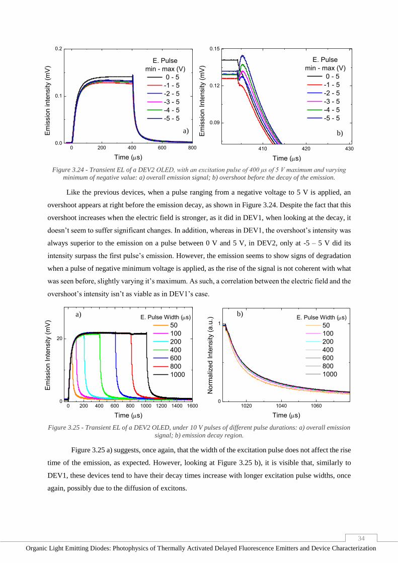
34
Organic Light Emitting Diodes: Photophysics of Thermally Activated Delayed Fluorescence Emitters and Device Characterization
0 200 400 600 8000.0
0.1
0.2E
mis
sio
n inte
nsity (
mV
)
Time (s)
E. Pulse
min - max (V)
0 - 5
-1 - 5
-2 - 5
-3 - 5
-4 - 5
-5 - 5
410 420 430
0.09
0.12
0.15
E. Pulse
min - max (V)
0 - 5
-1 - 5
-2 - 5
-3 - 5
-4 - 5
-5 - 5
Em
issio
n Inte
nsity (
mV
)
Time (s)
Figure 3.24 - Transient EL of a DEV2 OLED, with an excitation pulse of 400 μs of 5 V maximum and varying
minimum of negative value: a) overall emission signal; b) overshoot before the decay of the emission.
Like the previous devices, when a pulse ranging from a negative voltage to 5 V is applied, an
overshoot appears at right before the emission decay, as shown in Figure 3.24. Despite the fact that this
overshoot increases when the electric field is stronger, as it did in DEV1, when looking at the decay, it
doesn’t seem to suffer significant changes. In addition, whereas in DEV1, the overshoot’s intensity was
always superior to the emission on a pulse between 0 V and 5 V, in DEV2, only at -5 – 5 V did its
intensity surpass the first pulse’s emission. However, the emission seems to show signs of degradation
when a pulse of negative minimum voltage is applied, as the rise of the signal is not coherent with what
was seen before, slightly varying it’s maximum. As such, a correlation between the electric field and the
overshoot’s intensity isn’t as viable as in DEV1’s case.
0 200 400 600 800 1000 1200 1400 16000
20
E. Pulse Width (s)
50
100
200
400
600
800
1000
Em
issio
n Inte
nsity (
mV
)
Time (s)
1020 1040 10600
1E. Pulse Width (s)
50
100
200
400
600
800
1000
No
rmaliz
ed Inte
nsity (
a.u
.)
Time (s)
Figure 3.25 - Transient EL of a DEV2 OLED, under 10 V pulses of different pulse durations: a) overall emission
signal; b) emission decay region.
Figure 3.25 a) suggests, once again, that the width of the excitation pulse does not affect the rise
time of the emission, as expected. However, looking at Figure 3.25 b), it is visible that, similarly to
DEV1, these devices tend to have their decay times increase with longer excitation pulse widths, once
again, possibly due to the diffusion of excitons.
b) a)
a) b)
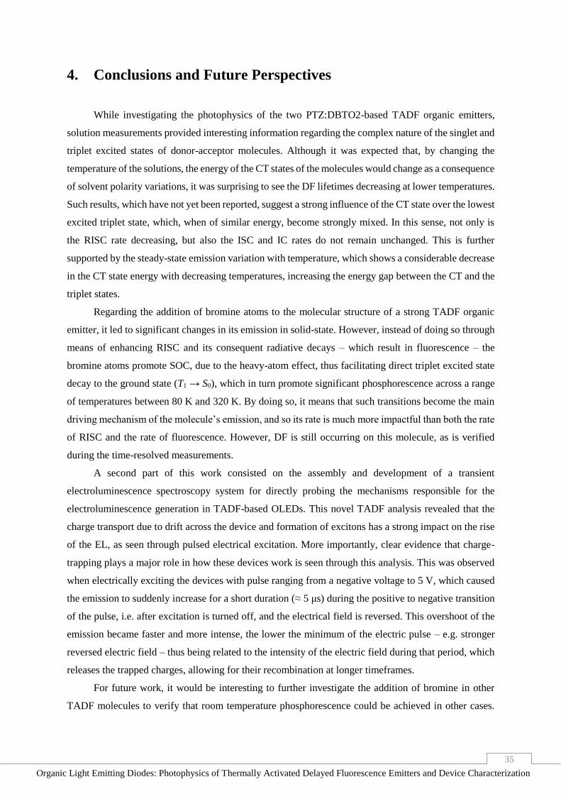
35
Organic Light Emitting Diodes: Photophysics of Thermally Activated Delayed Fluorescence Emitters and Device Characterization
4. Conclusions and Future Perspectives
While investigating the photophysics of the two PTZ:DBTO2-based TADF organic emitters,
solution measurements provided interesting information regarding the complex nature of the singlet and
triplet excited states of donor-acceptor molecules. Although it was expected that, by changing the
temperature of the solutions, the energy of the CT states of the molecules would change as a consequence
of solvent polarity variations, it was surprising to see the DF lifetimes decreasing at lower temperatures.
Such results, which have not yet been reported, suggest a strong influence of the CT state over the lowest
excited triplet state, which, when of similar energy, become strongly mixed. In this sense, not only is
the RISC rate decreasing, but also the ISC and IC rates do not remain unchanged. This is further
supported by the steady-state emission variation with temperature, which shows a considerable decrease
in the CT state energy with decreasing temperatures, increasing the energy gap between the CT and the
triplet states.
Regarding the addition of bromine atoms to the molecular structure of a strong TADF organic
emitter, it led to significant changes in its emission in solid-state. However, instead of doing so through
means of enhancing RISC and its consequent radiative decays – which result in fluorescence – the
bromine atoms promote SOC, due to the heavy-atom effect, thus facilitating direct triplet excited state
decay to the ground state (T1 → S0), which in turn promote significant phosphorescence across a range
of temperatures between 80 K and 320 K. By doing so, it means that such transitions become the main
driving mechanism of the molecule’s emission, and so its rate is much more impactful than both the rate
of RISC and the rate of fluorescence. However, DF is still occurring on this molecule, as is verified
during the time-resolved measurements.
A second part of this work consisted on the assembly and development of a transient
electroluminescence spectroscopy system for directly probing the mechanisms responsible for the
electroluminescence generation in TADF-based OLEDs. This novel TADF analysis revealed that the
charge transport due to drift across the device and formation of excitons has a strong impact on the rise
of the EL, as seen through pulsed electrical excitation. More importantly, clear evidence that charge-
trapping plays a major role in how these devices work is seen through this analysis. This was observed
when electrically exciting the devices with pulse ranging from a negative voltage to 5 V, which caused
the emission to suddenly increase for a short duration (≈ 5 μs) during the positive to negative transition
of the pulse, i.e. after excitation is turned off, and the electrical field is reversed. This overshoot of the
emission became faster and more intense, the lower the minimum of the electric pulse – e.g. stronger
reversed electric field – thus being related to the intensity of the electric field during that period, which
releases the trapped charges, allowing for their recombination at longer timeframes.
For future work, it would be interesting to further investigate the addition of bromine in other
TADF molecules to verify that room temperature phosphorescence could be achieved in other cases.
36
Organic Light Emitting Diodes: Photophysics of Thermally Activated Delayed Fluorescence Emitters and Device Characterization
Moreover, further research is needed to better comprehend the mixing character of the CT and lowest
triplet excited states suggested in this thesis, as it would allow for a more efficient design of TADF
molecules.
In addition to the photophysics work, it is of immense value to continue with the transient EL
spectroscopy, not only by investigating TADF-based OLEDs with different molecules, but to also
adapting the technique to study the devices’ behaviour with multiple-voltage-steps excitation pulses, but
also by allowing for measurements at different temperatures to be done. By doing so, it could be possible
to get a better insight on the charge trapping mechanism and, perhaps, observe other mechanisms
contributing to the emission process of the devices.
37
Organic Light Emitting Diodes: Photophysics of Thermally Activated Delayed Fluorescence Emitters and Device Characterization
References
[1] Baldo, M.A., Thompson, M.E., Forrest, S.R., "High-efficiency fluorescent organic light-emitting
devices using a phosphorescent sensitizer", Nature, vol. 403, 750–753, 2000.
[2] Dias, F.B., "Kinetics of Thermal-Assisted Delayed Fluorescence in Blue Organic Emitters with
Large Singlet-Triplet Energy Gap", Philosophical Transactions of the Royal Society A, vol. 373,
1–10, 2015.
[3] Uoyama, H., Goushi, K., Shizu, K., Nomura, H., Adachi, C., "Highly efficient organic light-
emitting diodes from delayed fluorescence", Nature, Nature Publishing Group, vol. 492, 234–
238, 2012.
[4] Monkman, A.P., "Singlet Generation from Triplet Excitons in Fluorescent Organic Light-
Emitting Diodes", ISRN Materials Science, vol. 2013, 1–14, 2012.
[5] Dias, F.B., Penfold, T.J., Monkman, A.P., "Photophysics of thermally activated delayed
fluorescence molecules", Methods and Applications in Fluorescence, IOP Publishing, vol. 5, 1–
25, 2017.
[6] Zhang, Q., Li, J., Shizu, K., Huang, S., Hirata, S., Miyazaki, H., Adachi, C., "Design of Efficient
Thermally Activated Delayed Fluorescence Materials for Pure Blue Organic Light Emitting
Diodes", Journal of the American Chemical Society, 1–4, 2012.
[7] Dias, F.B., Bourdakos, K.N., Jankus, V., Moss, K.C., Kamtekar, T., Bhalla, V., Santos, J., Bryce,
M.R., Monkman, A.P., "Triplet Harvesting with 100% Efficiency by Way of Thermally Activated
Delayed Fluorescence in Charge Transfer OLED Emitters", Advanced Materials, vol. 25, 27,
3707–3714, 2013.
[8] Im, Y., Lee, J.Y., "Above 20% External Quantum Efficiency in Thermally Activated Delayed
Fluorescence Device Using Furodipyridine-Type Host Materials", Chemistry of Materials, vol.
26, 1413–1419, 2014.
[9] Hebner, T.R., Wu, C.C., Marcy, D., Lu, M.H., Sturm, J.C., Hebner, T.R., Wu, C.C., Marcy, D.,
Lu, M.H., Sturm, J.C., "Ink-jet printing of doped polymers for organic light emitting devices",
Applied Physics Letters, vol. 72, 5, 519–521, 1998.
[10] Bharathan, J., Yang, Y., "Polymer electroluminescent devices processed by inkjet printing: I .
Polymer light-emitting logo", Applied Physics Letters, vol. 72, 21, 2660–2662, 1998.
[11] Choi, M., Kim, Y., Ha, C.-S., "Polymers for flexible displays: From material selection to device
applications", Progress in Polymer Science, vol. 33, 581–630, 2008.
[12] Cook, J., "The Investigation of Phosphorescent Dopants and Novel Blue Fluorescent Polymer
Hosts for PLED Devices", Durham University, 2015.
[13] Grimsdale, A.C., Chan, K.L., Martin, R.E., Jokisz, P.G., Holmes, A.B., "Synthesis of Light-
Emitting Conjugated Polymers for Applications in Electroluminescent Devices", Chemical
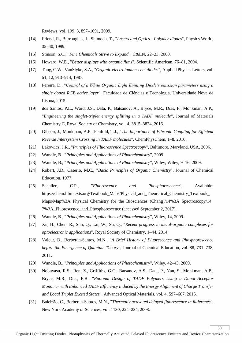
38
Organic Light Emitting Diodes: Photophysics of Thermally Activated Delayed Fluorescence Emitters and Device Characterization
Reviews, vol. 109, 3, 897–1091, 2009.
[14] Friend, R., Burroughes, J., Shimoda, T., "Lasers and Optics - Polymer diodes", Physics World,
35–40, 1999.
[15] Stinson, S.C., "Fine Chemicals Strive to Expand", C&EN, 22–23, 2000.
[16] Howard, W.E., "Better displays with organic films", Scientific American, 76–81, 2004.
[17] Tang, C.W., VanSlyke, S.A., "Organic electroluminescent diodes", Applied Physics Letters, vol.
51, 12, 913–914, 1987.
[18] Pereira, D., "Control of a White Organic Light Emitting Diode’s emission parameters using a
single doped RGB active layer", Faculdade de Ciências e Tecnologia, Universidade Nova de
Lisboa, 2015.
[19] dos Santos, P.L., Ward, J.S., Data, P., Batsanov, A., Bryce, M.R., Dias, F., Monkman, A.P.,
"Engineering the singlet-triplet energy splitting in a TADF molecule", Journal of Materials
Chemistry C, Royal Society of Chemistry, vol. 4, 3815–3824, 2016.
[20] Gibson, J., Monkman, A.P., Penfold, T.J., "The Importance of Vibronic Coupling for Efficient
Reverse Intersystem Crossing in TADF molecules", ChemPhysChem, 1–8, 2016.
[21] Lakowicz, J.R., "Principles of Fluorescence Spectroscopy", Baltimore, Maryland, USA, 2006.
[22] Wandle, B., "Principles and Applications of Photochemistry", 2009.
[23] Wandle, B., "Principles and Applications of Photochemistry", Wiley, Wiley, 9–16, 2009.
[24] Robert, J.D., Caserio, M.C., "Basic Principles of Organic Chemistry", Journal of Chemical
Education, 1977.
[25] Schaller, C.P., "Fluorescence and Phosphorescence", Available:
https://chem.libretexts.org/Textbook_Maps/Physical_and_Theoretical_Chemistry_Textbook_
Maps/Map%3A_Physical_Chemistry_for_the_Biosciences_(Chang)/14%3A_Spectroscopy/14.
7%3A_Fluorescence_and_Phosphorescence (accessed September 2, 2017).
[26] Wandle, B., "Principles and Applications of Photochemistry", Wiley, 14, 2009.
[27] Xu, H., Chen, R., Sun, Q., Lai, W., Su, Q., "Recent progress in metal-organic complexes for
optoelectronic applications", Royal Society of Chemistry, 1–44, 2014.
[28] Valeur, B., Berberan-Santos, M.N., "A Brief History of Fluorescence and Phosphorescence
before the Emergence of Quantum Theory", Journal of Chemical Education, vol. 88, 731–738,
2011.
[29] Wandle, B., "Principles and Applications of Photochemistry", Wiley, 42–43, 2009.
[30] Nobuyasu, R.S., Ren, Z., Griffiths, G.C., Batsanov, A.S., Data, P., Yan, S., Monkman, A.P.,
Bryce, M.R., Dias, F.B., "Rational Design of TADF Polymers Using a Donor-Acceptor
Monomer with Enhanced TADF Efficiency Induced by the Energy Alignment of Charge Transfer
and Local Triplet Excited States", Advanced Optical Materials, vol. 4, 597–607, 2016.
[31] Baleizão, C., Berberan-Santos, M.N., "Thermally activated delayed fluorescence in fullerenes",
New York Academy of Sciences, vol. 1130, 224–234, 2008.
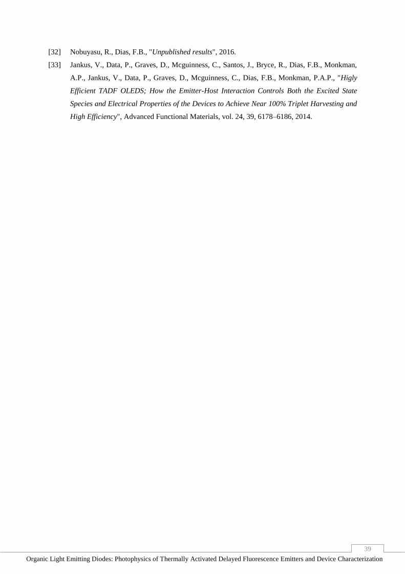
39
Organic Light Emitting Diodes: Photophysics of Thermally Activated Delayed Fluorescence Emitters and Device Characterization
[32] Nobuyasu, R., Dias, F.B., "Unpublished results", 2016.
[33] Jankus, V., Data, P., Graves, D., Mcguinness, C., Santos, J., Bryce, R., Dias, F.B., Monkman,
A.P., Jankus, V., Data, P., Graves, D., Mcguinness, C., Dias, F.B., Monkman, P.A.P., "Higly
Efficient TADF OLEDS; How the Emitter-Host Interaction Controls Both the Excited State
Species and Electrical Properties of the Devices to Achieve Near 100% Triplet Harvesting and
High Efficiency", Advanced Functional Materials, vol. 24, 39, 6178–6186, 2014.

40
Organic Light Emitting Diodes: Photophysics of Thermally Activated Delayed Fluorescence Emitters and Device Characterization
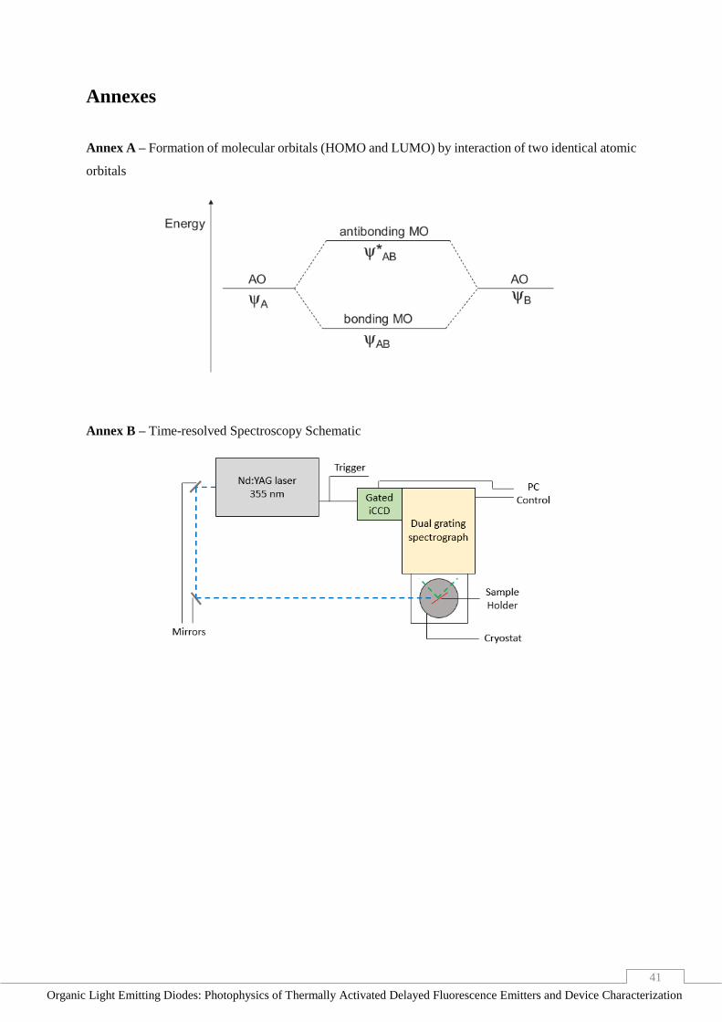
41
Organic Light Emitting Diodes: Photophysics of Thermally Activated Delayed Fluorescence Emitters and Device Characterization
Annexes
Annex A – Formation of molecular orbitals (HOMO and LUMO) by interaction of two identical atomic
orbitals
Annex B – Time-resolved Spectroscopy Schematic
42
Organic Light Emitting Diodes: Photophysics of Thermally Activated Delayed Fluorescence Emitters and Device Characterization
Annex C – Molecular Weight Addition Influence on the Absorption Spectra
To verify the effect of the molecular weight on the D fragment seen in section 3.1.1, experiments
were also conducted with the A fragment, having collected its absorption spectra and the spectra of its
analogue containing methyl chains.
Similar to the D fragment presented in section 3.1.1, in Figure 5.2 it is possible to observe that
the methyl chains caused an increase in the extinction coefficient of the A fragment, accompanied by a
red-shift of its absorption peaks, serving as further evidence that the addition of bromine groups should,
indeed, have the same effect.
250 300 3500
1
2
3
4
5
Molecule
A
A'
x 1
04 (
L m
ol -
1 c
m-1)
Wavelength (nm)
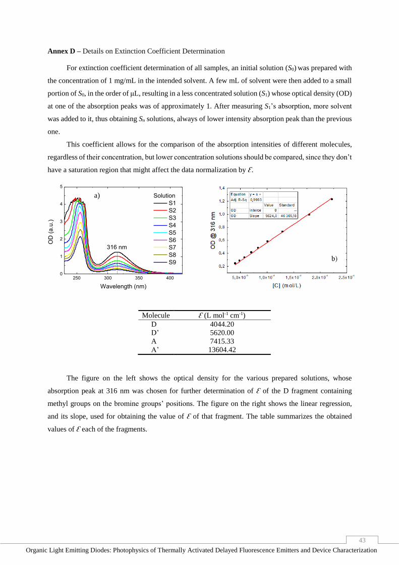
43
Organic Light Emitting Diodes: Photophysics of Thermally Activated Delayed Fluorescence Emitters and Device Characterization
Annex D – Details on Extinction Coefficient Determination
For extinction coefficient determination of all samples, an initial solution (S0) was prepared with
the concentration of 1 mg/mL in the intended solvent. A few mL of solvent were then added to a small
portion of S0, in the order of μL, resulting in a less concentrated solution (S1) whose optical density (OD)
at one of the absorption peaks was of approximately 1. After measuring S1’s absorption, more solvent
was added to it, thus obtaining Sn solutions, always of lower intensity absorption peak than the previous
one.
This coefficient allows for the comparison of the absorption intensities of different molecules,
regardless of their concentration, but lower concentration solutions should be compared, since they don’t
have a saturation region that might affect the data normalization by Ɛ.
250 300 350 4000
1
2
3
4
5
OD
(a.u
.)
Wavelength (nm)
Solution
S1
S2
S3
S4
S5
S6
S7
S8
S9
316 nm
The figure on the left shows the optical density for the various prepared solutions, whose
absorption peak at 316 nm was chosen for further determination of Ɛ of the D fragment containing
methyl groups on the bromine groups’ positions. The figure on the right shows the linear regression,
and its slope, used for obtaining the value of Ɛ of that fragment. The table summarizes the obtained
values of Ɛ each of the fragments.
Molecule Ɛ (L mol-1 cm-1)
D 4044.20
D’ 5620.00
A 7415.33
A’ 13604.42
a)
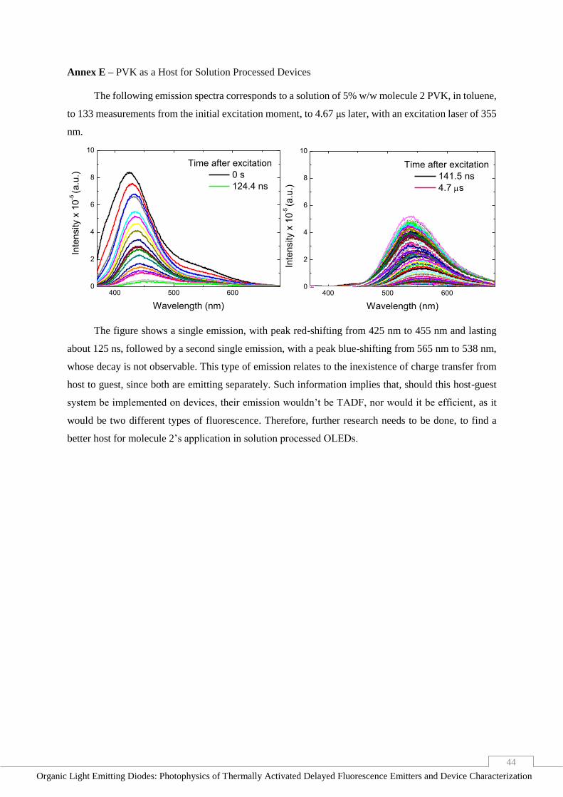
44
Organic Light Emitting Diodes: Photophysics of Thermally Activated Delayed Fluorescence Emitters and Device Characterization
Annex E – PVK as a Host for Solution Processed Devices
The following emission spectra corresponds to a solution of 5% w/w molecule 2 PVK, in toluene,
to 133 measurements from the initial excitation moment, to 4.67 μs later, with an excitation laser of 355
nm.
400 500 6000
2
4
6
8
10
Time after excitation
0 s
124.4 ns
Inte
nsity x
10
-5 (a
.u.)
Wavelength (nm)
400 500 6000
2
4
6
8
10
Time after excitation
141.5 ns
4.7 s
Inte
nsity x
10
-5 (a
.u.)
Wavelength (nm)
The figure shows a single emission, with peak red-shifting from 425 nm to 455 nm and lasting
about 125 ns, followed by a second single emission, with a peak blue-shifting from 565 nm to 538 nm,
whose decay is not observable. This type of emission relates to the inexistence of charge transfer from
host to guest, since both are emitting separately. Such information implies that, should this host-guest
system be implemented on devices, their emission wouldn’t be TADF, nor would it be efficient, as it
would be two different types of fluorescence. Therefore, further research needs to be done, to find a
better host for molecule 2’s application in solution processed OLEDs.