Embed Size (px)
Citation preview

ARTICLE
Origami silicon optoelectronics for hemisphericalelectronic eye systemsKan Zhang1, Yei Hwan Jung 1, Solomon Mikael1, Jung-Hun Seo 1, Munho Kim1, Hongyi Mi1, Han Zhou1,
Zhenyang Xia1, Weidong Zhou2, Shaoqin Gong3 & Zhenqiang Ma1
Digital image sensors in hemispherical geometries offer unique imaging advantages over their
planar counterparts, such as wide field of view and low aberrations. Deforming miniature
semiconductor-based sensors with high-spatial resolution into such format is challenging.
Here we report a simple origami approach for fabricating single-crystalline silicon-based focal
plane arrays and artificial compound eyes that have hemisphere-like structures. Convex
isogonal polyhedral concepts allow certain combinations of polygons to fold into spherical
formats. Using each polygon block as a sensor pixel, the silicon-based devices are shaped into
maps of truncated icosahedron and fabricated on flexible sheets and further folded either into
a concave or convex hemisphere. These two electronic eye prototypes represent simple and
low-cost methods as well as flexible optimization parameters in terms of pixel density and
design. Results demonstrated in this work combined with miniature size and simplicity of the
design establish practical technology for integration with conventional electronic devices.
DOI: 10.1038/s41467-017-01926-1 OPEN
1 Department of Electrical and Computer Engineering, University of Wisconsin–Madison, Madison, WI 53706, USA. 2Department of Electrical Engineering,University of Texas at Arlington, Arlington, TX 79019, USA. 3 Department of Biomedical Engineering and Wisconsin Institutes for Discovery, University ofWisconsin–Madison, Madison, WI 53706, USA. Kan Zhang, Yei Hwan Jung and Solomon Mikael contributed equally to this work. Correspondence andrequests for materials should be addressed to Z.M. (email: [email protected])
NATURE COMMUNICATIONS |8: 1782 |DOI: 10.1038/s41467-017-01926-1 |www.nature.com/naturecommunications 1
1234
5678
90
B iological eyes are highly sophisticated and remarkablydesigned vision organs that have inspired biomimicry forseveral centuries. From lobster eye-inspired radiant heaters
to moth eye-inspired anti-reflective coatings, human challengeshave been solved by nature’s advice in a wide variety of appli-cations1, 2. Also, the camera, which is undoubtedly the mostrevolutionary invention of mankind inspired by the eye, hasimmensely comforted, amused, and protected human lives.Today, technological advances have improved the quality ofcameras with superior resolution, long focal lengths, and smartfunctionalities that are implemented in almost every consumerelectronics system. In addition to these evolutions, reshapingconventional planar sensor systems into hemispherical formatswould empower visual recordings with features that are beyondwhat state-of-the-art cameras can see, such as infinite depth offield, wider view angle, and lower aberrations3. Studying variouseye systems in biology, most eyes have photoreceptors that
capture and transduce photons into electrochemical signals laideither in concave or convex curvature. The concave array ismostly found in mammals as a camera or pin-hole type while theconvex array is found in insects as a compound type. The cameraor pin-hole eye has an outstanding quality of vision as it focuseslight into an array of photoreceptors laid in a hemisphericalconcave structure (i.e., retina), allowing for clear identificationof objects. The retina adopts the curvilinear shape that approx-imates the focal plane of the lens such that human eyes havelarge view fields and supreme focusing capabilities4. The com-pound eye has a wider-angle field of view via hundreds tothousands of ommatidia that are densely arrayed in a hemi-spherical convex structure for the sensitive detection of movingobjects5. As such, biomimicry using semiconductor sensor sys-tems structured in hemispherical formats would extend thecapabilities of camera systems by utilizing the marvelous featuresof biological eyes.
a b
dc
e f
Concave Convex
Fig. 1 Geometric origami of silicon optoelectronics for the hemispherical electronic eye. a Schematic illustration of the net of half truncated icosahedronbeing folded into a hemisphere. 676 polygon blocks consisting of pentagons and hexagons were mapped into a net of subdivided half truncatedicosahedron which was then folded to form a hemisphere. b A photograph of the half truncated icosahedron based on polygon blocks of metal-coatedsilicon nanomembranes printed on a flexible polyimide film. The completed net was folded into a convex hemisphere by inserting the net into a circular holeof a metal fixture. Scale bar, 1 mm. c Schematic illustration of the net of half truncated icosahedron based on silicon nanomembranes pressed into ahemispherical concave mold. d Schematic illustration of the net of half truncated icosahedron based on silicon nanomembranes covered on a hemisphericalconvex mold. e A photograph of a silicon optoelectronics-based hemispherical focal plane array formed using the concave mold-based origami approachshown in c. Inset image shows the flat focal plane array before folding. Scale bar, 2 mm. f A photograph of a silicon optoelectronics-based convexhemispherical eye camera formed using the convex mold-based origami approach shown in d. Inset image shows the flat eye camera before folding. Scalebar, 2 mm
ARTICLE NATURE COMMUNICATIONS | DOI: 10.1038/s41467-017-01926-1
2 NATURE COMMUNICATIONS | 8: 1782 |DOI: 10.1038/s41467-017-01926-1 |www.nature.com/naturecommunications

Although numerous types of artificial eyes have been presentedin the past, the inspired systems lacked the essential photo-detecting unit6–9. To take advantage of mimicking biological eyesin electronic imaging systems, photodetectors must essentially berepresented in either hemispherical concave or convex formatsrather than in the planar format typically found in conventionalcamera systems. Fabricating devices on non-planar surfaces,however, can be a major challenge because conventional fabri-cation techniques were developed for planar wafers or platematerials in the semiconductor industry. The simplest approachto deforming sensors was to mount optoelectronic componentson a flexible printed-circuit board (FPCB), but this could onlyachieve hemicylindrical photodetector array designs10. Specia-lized techniques to apply stress on and bend ordinary planarsilicon wafer-based CMOS image sensors have been introduced aswell, which have been successful in inducing minor curvatures11,12. The available techniques for direct fabrication on non-planarsurfaces, such as soft lithography, mechanical molding, and lens-assisted lithography, are consequently complicated and expensive,and have very specific requirements. Encouraged by the pro-mising prosperity in non-planar devices, novel strategies havebeen investigated to circumvent the limits set by non-planarsurfaces while utilizing mature semiconductor fabrication tech-niques for economic consideration. For instance, transfer printingof ultrathin semiconductor nanomembranes onto rubber- orplastic-like substrates transformed the shape of high-performanceelectronics and optoelectronics into flexible and stretchable for-mats13–18. These unusual semiconductor devices on complexcurvilinear surfaces are versatile in various areas due to their newdegree of design freedom and biomimicry merits, including thehemispherical photodetector array19–23. Successful integration ofstretchable photodetectors with camera systems has demon-strated concave and convex curvilinear photodetector arrays forthe hemispherical electronic eye camera that mimicked thehuman eye21 and compound electronic eye camera thatmimicked the arthropod eye22. In both designs, a large array ofthin silicon photodiodes separated by serpentine traces of metalfor electrical interconnects were originally fabricated on a planarhost substrate and transfer-printed onto rubber substrates. Uponhydraulic actuation, the array on rubber deformed and stretchedinto either a concave or convex structure, where the geometry ofthe serpentine wire tortuosity deterministically transformed thelayout without electrical or mechanical failure. Both concave andconvex camera systems that used silicon optoelectronics weregroundbreaking toward camera evolution, but the requirement ofhydraulic actuators may be bulky in many miniaturized camerasystems for consumer devices. Also, the large separation distancebetween photodetector pixels reserved for electrical traces that arein the micrometer range may pose limitations in resolutionoptimization. An approach that is both compatible with com-mercially available imaging systems and has flexible optimizationparameters is desirable for such hemispherical photodetectorarrays to become more practical.
Here, we present a unique origami-inspired approach, com-bined with semiconductor nanomembrane-based flexible elec-tronics technology, to build dense, scalable, and compacthemispherical photodetector arrays. Originated as an art of paperfolding, origami and kirigami were recently utilized to assemblethree-dimensional structures with micro/nanomembrane mate-rials to allow an increasingly wide range of applications24–28.Precut membranes have been structured into numerous types ofinteresting three-dimensional assemblies via buckling and foldingto form various electronic components, including antennas, solarcells, batteries, nanogenerators, waveguides, photodetectors, andmetamaterials29–37. Although a similar approach of formingcurved silicon photodetector hemisphere was introduced in the
past, optical imaging using the hemisphere array has not yet beendemonstrated38. In this work, the folding mechanism is imple-mented for both concave and convex curvilinear photodetectorarrays with single-crystalline silicon nanomembranes. The lowflexural rigidity of single-crystalline nanomembrane allows high-performance photodetectors to bend with microscale radius ofcurvature39. Combining the origami-inspired approach with thetransfer printing of advanced inorganic nanomembranes onflexible substrates, high-performance hemispherical electronic eyecamera systems are fabricated to allow for unusual imaging thatcould not be done with conventional camera systems. Further-more, the origami-based fabrication eliminates the use of metalwires in-between pixels for the connection of sparsely arrayeddevices (as seen in other similar systems that limited resolutionoptimizations), as well as eliminating the need for the sophisti-cated actuators that were used to form the hemispheres21, 22.
ResultsGeometric origami for hemisphere-like silicon optoelectronics.Figure 1 illustrates the concept of geometric origami used for thephotodetector array. In geometry mathematics, a quasi-sphericalsolid is formed using one of the renowned Archimedean solids—the truncated icosahedron—which is a combination of multiplepentagonal and hexagonal faces, typically found in soccer balls orbuckminsterfullerene molecules. As presented in SupplementaryFig. 1a, a net of half truncated icosahedron was first mapped andcut on the flexible substrate, followed by folding the net to create aquasi-hemisphere. The edges of the hemisphere-like structurecould be further smoothed out by dividing the large pentagonaland hexagonal faces into even smaller polygon faces as presentedin Supplementary Fig. 1b. The subdivided icosahedron not onlysmoothed out the edges of the hemisphere, but also allowed morepixels inside the geometry to improve fidelity. As an example,Fig. 1a represents a schematic illustration where the 676 polygonblocks were mapped into a net of subdivided half truncated ico-sahedron which was then folded to form a hemisphere. Figure 1bshows a photograph of the folded truncated icosahedron usingmetallized silicon nanomembrane blocks, printed onto a flexiblepolyimide substrate. The entire microfabrication of electronicdevices, including silicon etch, metal deposition, and device pas-sivation, were completed in a planar format prior to deformation,simplifying the process flow of curvilinear semiconductor devicesby leaving the deformation mounting to the last step and thuspreserving the feasibility of most semiconductor fabricationtechniques. As a result, a simple and practical method to integratewell-developed planar devices onto complex curvilinear surfaceswas achieved, enabling diverse applications that were difficult toaddress using conventional means. As presented in Fig. 1c, d, thenet may be folded upwards for a concave hemisphere or down-wards for a convex hemisphere. For instance, the concave arraymay be used to mimic the retina in either pin-hole- or camera-type mammalian eyes while the convex array may be used tomimic the ommatidia in a compound eye. Using nanomembranescombined with flexible substrates, the ultrathin photodetectorarray further bends to yield a smooth hemisphere. Figure 1e, frepresents the abovementioned concave and convex photodetectorarrays, respectively, using the origami approach. They were thenanalyzed and are discussed in detail here in later sections.
Si nanomembrane-based photodiodes for origami optoelec-tronics. Silicon-based lateral P–i–N photodiodes were used assensors in this study due to their broad spectrum, as well as thelarge bandgap of silicon and the fast response of the P–i–Nstructure. The schematic illustration shown in Fig. 2a and theoptical microscope image in Fig. 2b represent the photodetector
NATURE COMMUNICATIONS | DOI: 10.1038/s41467-017-01926-1 ARTICLE
NATURE COMMUNICATIONS |8: 1782 |DOI: 10.1038/s41467-017-01926-1 |www.nature.com/naturecommunications 3
unit implemented in the electronic eyes. The photosensitivityresults of the photodetector diode are shown in Fig. 2c. Themeasured dark current density was lower than 1 × 10⁻¹⁴ A μm−2
up to a –5 V bias and weakly dependent on the reverse-biasvoltage. The photocurrents measured at –3 V under the illumi-nation of three visible lasers, including green (543 nm), yellow(594 nm), and red (633 nm) lasers were 1.74 × 10⁻¹¹ A μm−2,1.21 × 10−11 A μm−2, and 1.95 × 10⁻¹¹ A μm−2, respectively. Themeasured current densities of the photodetectors at the differentpower levels exposed with each visible laser are shown in Sup-plementary Fig. 2a–c. The ratio between the photocurrent and thedark current showed about a 104 fold difference. The calculatedphoto responsivity was 9.49 mAW−1, 6.24 mAW−1, and 5.26mAW−1 at –3 V under the green, yellow, and red lasers,respectively, as shown in Fig. 2d. The external quantum efficiency(EQE) was calculated using the photocurrent and the incidentlight power. At –3 V, the EQE was 2.2%, 1.3% and 1.0% for thegreen, yellow, and red lasers, respectively. Imaging with thesephotodetectors was performed using the green laser, as thephotodiodes were most responsive to green light.
Origami optoelectronics for hemispherical focal plane array.Figure 3a presents a schematic illustration of the hemisphericalfocal plane array (FPA) based on origami silicon optoelectronics.The array was designed such that the pixels were laid out to forma large net of subdivided half truncated icosahedron, where eachpixel contained a single photodetector and was shaped into eithera pentagon or a hexagon, and electrically connected by metalinterconnects. A macroscopic view of the hemisphere formedwith this combination of polygons is represented with paperorigami, as presented in Supplementary Fig. 3. In total, there were281 photodetectors in the hemispherical array, and each wasadjacent to one another. The inner diameter of a single hexagonalphotodetector was 113 μm, as presented in SupplementaryFig. 2d. The net was first fabricated on a planar format whereconventional optoelectronics processes involving high tempera-tures and chemical solvents were utilized and transfer-printed
onto a flexible polyimide substrate. Once the fabrication andpassivation of the device was complete, the flexible net of halftruncated icosahedron was mounted onto a concave fixture tomechanically transform it into a hemisphere. To precisely mountand fold the net onto a fixture, a metal-based hemisphere (con-cave) fixture and a polydimethylsiloxane (PDMS)-based reverse(convex)-hemisphere pressing mold were prepared. The net wascentered onto the reverse mold, where the adhesion of the PDMS-based reverse mold temporarily held the net during the mountingprocess. The mounting process was completed by coating themetal concave fixture with a thin layer of epoxy glue and gentlypressing the reverse mold with device onto the fixture. This pro-cess flow is applicable to curvilinear surfaces with different cur-vatures and was verified by mounting the net onto two concavefixtures with different radii (r = 2.27 mm and 7.20 mm) of curva-ture of the hemisphere, as presented in Supplementary Fig. 4.Supplementary Fig. 4a and b describes the detailed design para-meters of the metal concave fixtures with small and large radii,respectively. During the mounting process, mechanical deforma-tion was introduced to each pixel. However, the low flexuralrigidity from the extremely small thickness of the silicon nano-membrane used as the photodetector material allowed themechanical deformation to have a negligible impact on the per-formance of the device40. The performance of the photodetectorstarted to degrade when the radius of curvature reached 1.5mm,as presented in Supplementary Fig. 5. The layer thicknesses of thesilicon nanomembrane, metal interconnects, and polymer passi-vations can be reduced to achieve curvilinear photodetector arrayswith smaller radius of curvature. For instance, a 20 nm thicksilicon nanomembrane photodetector could wrap around thecladding layer of a single mode fiber to detect light leakage, whichtypically has a diameter of 125 μm39. It is important to carefullycontrol the mechanical neutral plane of the device, such thatminimal stress is applied on the most fragile part of the device13.
A simple camera system using a hemispherical FPA wasassembled as presented in Fig. 3b. A plano-convex lens (10 mmdiameter and 10 mm focal length) that focused light was placedin-between the array and the image. Figure 3c shows a
–3 –2 –1 0 110–17
10–15
10–13
10–11
10–9
Yellow 594 nm
Red 633 nm
DarkGreen 543 nm
Cur
rent
den
sity
(A/µ
m2 )
Voltage (V)
–3 –2 –1 005
10152025303540
Resp. Green Resp. Yellow Resp. Red
EQE Green EQE Yellow EQE Red
Voltage (V)
Res
pons
ivity
(m
A/W
)
0.0
0.5
1.0
1.5
2.0
2.5
Ext
erna
l qua
ntum
effic
ienc
y (%
)
P+ SiN+ Si
Interconnect
a
b
c
d
Intrinsic Si
Fig. 2 Electrical properties of a silicon optoelectronic device used for the electronic eyes. a Schematic illustration of a hexagon-shaped siliconnanomembrane-based photodiode used for the electronic eyes. An array of such photodiodes were printed and fabricated on a pre-cut flexible polyimidesubstrate. b Optical microscope image of the photodiodes. Scale bar, 50 μm. c Current density–voltage characteristics of the photodiode in the dark andunder the illumination of lasers with wavelengths of 543 (green), 594 (yellow), and 633 nm (red). d Responsivity and external quantum efficiency of thephotodiode under the illumination of lasers with green, yellow, and red wavelengths. The laser light intensities were 5mW for the green and yellowwavelengths and 7 mW for the red wavelength. Green laser was used for the rest of this study
ARTICLE NATURE COMMUNICATIONS | DOI: 10.1038/s41467-017-01926-1
4 NATURE COMMUNICATIONS | 8: 1782 |DOI: 10.1038/s41467-017-01926-1 |www.nature.com/naturecommunications

photographic image of the FPA, with the inset image showing theassembled device including the plano-convex lens. Individualcomponents, including the laser, image, lens, photodetector array,etc., were placed on a rail and allowed for flexible adjustments tothe imaging setup, as shown in Supplementary Fig. 6. Figure 3drepresents the simulated focal plane of the camera system. Thedistance between the plano-convex lens and the focal plane arraywas approximated by simulating an object reflected on a planarfocal plane behind the lens. As shown in Supplementary Fig. 7,the focal plane from the planar plane of the lens was bestapproximated in the range of 7.0–8.5 mm, which agreed well withthe back focal length (8.18 mm) provided by the lens
manufacturer. With proper adjustments to the lens position,the focal plane had acceptable detection accuracy with thephotodiode array, as shown in the left inset plot in Fig. 3d.Imaging of the object was also performed with the FPA mountedon a larger radius of curvature (7.20 mm) to demonstrate theorigami photodetector array’s potential for hemispheres withvarious radii of curvatures. A plano-convex lens with a largerfocal length (10 mm diameter and 20 mm focal length) was usedfor the photodiode array with the larger radius (7.20 mm). Thefocal plane for the photodiode array with the larger radius (7.20mm) also had acceptable detection accuracy, as presented inSupplementary Fig. 8. In addition, the distance at which the
0 1 2 3 4 5 6 7 8 9 10 11 12O
bjec
t pla
ne
Position (cm)
0°
12°
24°
36°
60°
48°
LensPD array
–4 –3 –2 –1 0 1 2 3 4
0.0
0.5
1.0
1.5
z (m
m)
x (mm)
Lens focal planePD array
Lightsource
ImageLens
Hemisphericalfocal plane array
a b
c d
e
f
Lens
–1
z (m
m)
1
0
–1.5–1.0
–0.50
0.51.0
1.5 –1.5
–0.5 y (m
m)x (mm) –1.0
0
0.5
1.0
1.5
Ref.
Photodetector
Fig. 3 A concave hemispherical electronic eye camera system using origami silicon optoelectronics. a Schematic illustration of the hemispherical focalplane array (FPA) based on origami silicon optoelectronics. Fully formed photodiode array fabricated into a net of half truncated icosahedron was pressedand folded into a concave mold to create the hemispherical geometry. b Optics setup of the hemispherical electronic eye system shown using a schematicillustration with a light source, imaged object, and plano-convex lens to the left of the FPA. c A photograph of the hemispherical FPA based on origamisilicon optoelectronics. Inset image shows a photograph of the electronic eye system with the plano-convex lens integrated on top of the FPA. Scale bar, 1mm. d Ray patterns traced from different angles plotted against the position from the object plane. Right inset plot shows a magnified view of the dottedbox shown in the plot. Left inset shows the calculated focal plane of the ray passing through the plano-convex lens (dotted red curve) and measured focalplane of the silicon optoelectronics array (blue curve). e High-resolution image of the letter ‘W’ acquired from the hemispherical electronic eye camera.The image was scanned from 0° to 60° in 12° increments for the refined imaging. Each inset image shows a snapshot at each degree angle, with thereference photodiode highlighted in green. f High-resolution image of the letter ‘W’ acquired from the hemispherical electronic eye camera matching theconcave hemispherical surface of the FPA
NATURE COMMUNICATIONS | DOI: 10.1038/s41467-017-01926-1 ARTICLE
NATURE COMMUNICATIONS |8: 1782 |DOI: 10.1038/s41467-017-01926-1 |www.nature.com/naturecommunications 5
camera system should be placed was calculated using the raytraces plotted against the distance between the object and thecamera system. With the hemispherical focal plane’s radius ofcurvature fixed at 2.27 mm, the position of the plano-convex lenswas calculated to be 10.3 cm away from the object plane (for alarger radius of 7.20 mm, the distance was increased to 20 cm).
Figure 3e, f shows the images obtained from the hemisphericalFPA. Multiplexers allowed for the recording of signals from thelarge array of photodetectors in the matrix. The array ofphotodetectors with rows and columns of metal interconnectswas connected to ten CMOS analog multiplexer circuits, wheretwo 8-to-1 multiplexers controlled each side area of the halftruncated icosahedron net. Imaging using the photodetector arraywas controlled with a computer programmed design platform in apassive matrix format. The recording mechanism and themultiplexer layouts, as well as the printed-circuit board (PCB)layout, are presented in Supplementary Fig. 9. The dense array ofthe photodetectors imaged the letter ‘W’ with relatively high-spatial resolution. To further improve the image quality andeliminate the dark spots from defective pixels, a sequence ofimages was collected while rotating the imaged object. Imageswere taken after rotating the image counterclockwise in 12°increments from 0° to 60°. Ideally, the camera system should berotated, rather than the imaged object, as the object remainsstationary when a photo is taken. Rotation of the camera systemwas limited in the setup as shown in Supplementary Fig. 6, thusthe imaged object was rotated instead, mimicking the clockwiserotation of the camera system. A total of six images werecombined and reconstructed to obtain a scanned, improved-quality image as shown in the middle image of Fig. 3e. Each of thesix smaller images in Fig. 3e around the middle scanned imagerepresents single scanning at a given rotation angle, with thereference photodiode shown in green for easier visualization of
rotation. A high-resolution image of the letter ‘W’ acquired fromthe hemispherical electronic eye camera was rendered usingnumerical computing software to match the hemisphericalsurface of the FPA, as presented in Fig. 3f. It is expected thatan image with higher resolution may be achieved by increasingthe number of scans. The same set of experiments wereperformed for the photodetector array with the larger radius ofcurvature (7.20 mm). As presented in Supplementary Fig. 10, forthe larger radius of curvature, a slightly deteriorated and blurredletter was detected as compared to the image from the smallerradius, possibly due to optical aberrations associated with animperfect FPA and lens combination. It should also be noted thatthe design of truncated icosahedron was not optimized for such alarge radius of curvature, which created blind spots within theFPA. Nevertheless, the use of hemispherical FPAs largelybenefited from the simplified optical elements required to imagean object, as recording with planar FPA requires complicatedoptical systems to eliminate off-axis aberrations such asastigmatism, field curvature, and coma. This not only saved cost,but also allowed for a much simpler and compact camera design.
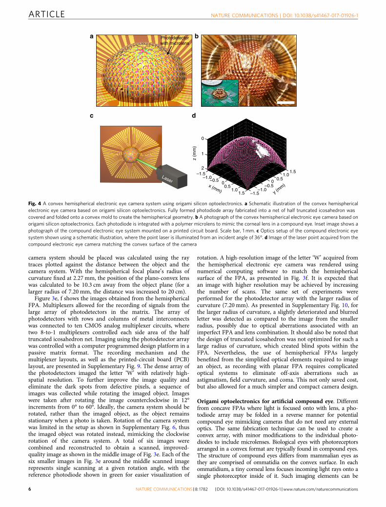
Origami optoelectronics for artificial compound eye. Differentfrom concave FPAs where light is focused onto with lens, a pho-todiode array may be folded in a reverse manner for potentialcompound eye mimicking cameras that do not need any externaloptics. The same fabrication technique can be used to create aconvex array, with minor modifications to the individual photo-diodes to include microlenses. Biological eyes with photoreceptorsarranged in a convex format are typically found in compound eyes.The structure of compound eyes differs from mammalian eyes asthey are comprised of ommatidia on the convex surface. In eachommatidium, a tiny corneal lens focuses incoming light rays onto asingle photoreceptor inside of it. Such imaging elements can be
a b
c d
z (m
m)
–1.5
–0.5–1.0
0 0.51.0
1.5–1.5
x (mm)
Laser
y (mm)
–1.0–0.5 0
0.51.0
1.5
2
0
1
Photodetectorwith microlens
Fig. 4 A convex hemispherical electronic eye camera system using origami silicon optoelectronics. a Schematic illustration of the convex hemisphericalelectronic eye camera based on origami silicon optoelectronics. Fully formed photodiode array fabricated into a net of half truncated icosahedron wascovered and folded onto a convex mold to create the hemispherical geometry. b A photograph of the convex hemispherical electronic eye camera based onorigami silicon optoelectronics. Each photodiode is integrated with a polymer microlens to mimic the corneal lens in a compound eye. Inset image shows aphotograph of the compound electronic eye system mounted on a printed circuit board. Scale bar, 1 mm. c Optics setup of the compound electronic eyesystem shown using a schematic illustration, where the point laser is illuminated from an incident angle of 36°. d Image of the laser point acquired from thecompound electronic eye camera matching the convex surface of the camera
ARTICLE NATURE COMMUNICATIONS | DOI: 10.1038/s41467-017-01926-1
6 NATURE COMMUNICATIONS | 8: 1782 |DOI: 10.1038/s41467-017-01926-1 |www.nature.com/naturecommunications

artificially created on top of each photodetector using the simplephotoresist reflow approach41–43. A microlens placed on top of eachdetecting unit maximizes the amount of light delivered to thephotodiode by accepting light from large incident angles (Supple-mentary Fig. 11). A slight decrease in incident light was observedwith the microlens at 0°, which was attributed to the lightabsorption in the photoresist, but the loss was negligible and thelens transmitted a higher incident light percentage at larger incidentangles. Whereas an actual ommatidium consists of other elements(like pigment cells and crystalline cones, in addition to the corneallens, that all together focus light and isolates itself from neighboringommatidia), the convex array demonstrated in this report lackssuch isolating elements. However, it shows the proof of concept thatcomplex elements like the corneal lens can be fabricated on thephotodetector array formed using the origami approach. Similar tothe concave hemispherical FPA, the hemispherical electronic eyethat was convex in shape was formed using the same net of sub-divided half truncated icosahedron, with a radius of curvature of2.27mm. With the photoresist microlens fabricated on top of eachphotodetector, the net was mounted on a convex fixture as shownin the schematic illustration in Fig. 4a. The mounting process forconvex array was completed by coating the convex fixture with athin layer of epoxy glue and pressing down the net with a reversemold. A photographic image of the device before being mounted onthe convex fixture is presented in Supplementary Fig. 12. Figure 4bshows a photographic image of the convex hemispherical electroniceye and its inset image shows the device mounted on the PCBsystem. To demonstrate its ability to image with a wide field of view,a narrow laser beam was fired at an angle of 36° from the PCBplane, as illustrated in Fig. 4c. Figure 4d shows the image of the laserlight acquired from the electronic eye camera matching the convexsurface of the photodetector array, with brighter regions indicatingthe photodetectors of the convex electronic eye camera thatdetected the laser light. Although the convex design of the photo-detector array enabled peripheral vision, the scanned image wascloser to a blurry spot rather than a detailed single point. This wasdue to the large acceptance angle of the device that led to anoverlapping of the light received by the adjacent diodes withmicrolenses. Additional biomimicry elements that isolated eachphotodiode and optimized acceptance versus inter-ommatidialangle could eliminate these adverse effects. As shown in this con-ceptual design, the convex hemispherical camera benefits from itscapability to detect light from wide angles without any need ofexternal optics like the camera-type eye. Such aspects are especiallyuseful for visually controlled navigation and optometer responsesthat do not necessarily require extreme resolution, but require wideview angles and minimized device layouts. With further optimiza-tions in the optical components by adding layers that mimic thepigment cells and crystalline cones, a compound electronic eyesystem that has panoramic vision may also be capable.
DiscussionThe biomimicry of eyes demonstrated in this report utilized thesimple origami approach of deforming flexible electronics intohemispherical formats, which successfully generated two veryimportant camera systems with a large number of photodetectors ina dense array. The density of the array can further be expanded bysplitting the polygon blocks into smaller blocks or by attachingmore pixels around the array. Moreover, the fabrication process canbe made compatible with existing CMOS sensor technology withextremely high densities by releasing the array of CMOS sensorsfabricated on silicon-on-insulator (SOI) wafers and origami-deforming the array at the last step. The conventional siliconmanufacturing techniques used to fabricate the photodetectors, aswell as the miniature size of the finished device, are beneficial to
advance such an approach into commercial electronic systems. Theeasily scalable pixel density and the simplicity of the device structureare the key features of this method. Future research includesdeveloping tunable hemispheres for the origami optoelectronics andmounting mechanisms for easy integration with other electronics.Furthermore, other convex isogonal polyhedral concepts, such asdodecahedron or rhombicosidodecahedron, may be employed asorigamis to create unusual optoelectronics or electronics in hemi-spherical formats. Applying this concept to state-of-the-art digitalcameras that capture high quality images or surveillance camerasusing infrared night vision are also desirable which would furtherexpand the capabilities of cameras.
MethodsFabrication of Si-based photodiodes on flexible film. The fabrication of bothconcave and convex hemispherical eyes started from a lightly p-doped SOI wafer(SOITECTM) which had a 270 nm device layer and 200 nm buried oxide (BOX)layer. The wafer was patterned and heavily doped with boron and phosphorus toform N+ and P+ regions using ion implantations (boron, dose of 4 × 1015 cm−2 andan energy of 20 KeV, and phosphorus, dose of 4 × 1015 cm−2 and an energy of 30KeV), followed by diffusion at 950 °C for 20 min in a 5% O2, 95% N2 ambientatmosphere. An array of etch-holes was made using photolithography and reactive-ion etching (RIE) to partially expose the BOX layer, and the processed top Sinanomembrane layer was released by immersing it in concentrated hydrofluoricacid (49%) for 2 h. A flexible polyimide film (Kapton HN; Dupont; 127 μm) wasprepared by laser cutting the film (A-laser) to match the half truncated icosahedronpattern of the array. The patterns of the photodiode array and flexible substrateboth corresponded to a shape consisting of one pentagon surrounded by fivehexagons, so that the finished array could be wrapped onto a hemispherical fixture.The Si nanomembrane was directly transferred onto the polyimide film by pressingthe adhesive-coated (SU-8 2; Microchem; 2 μm) polyimide film against the releasednanomembrane. During this process, a modified mask aligner (MJB-3; Karl Suss)was used to perfectly align and transfer the nanomembrane to the precut polyimidesubstrate. After curing the adhesive, the silicon nanomembrane was patterned andetched (RIE) into polygon blocks to isolate the pixels, and the SU-8 (SU-8 2;Microchem; 2 μm) passivation layer was patterned with via-holes, followed by thedeposition of first metal interconnects (Ti/Au = 30/250 nm). Adding another SU-8via-hole layer with second metal interconnects and the final SU-8 passivation layerconcluded the device fabrication process. These detailed processes are describedwith schematic illustrations in Supplementary Fig. 13.
Fabrication of polymer microlens for compound eye. For the convex hemi-spherical electronic eye, a microlens was fabricated on each SU-8 (4 μm) passivatedphotodiode for a wider view field. The fabrication involved photolithography of athick photoresist (AZ4620; MicroChemicals; 40 μm) and thermal reflow. Afterisolating the photoresist with photolithography, oven heating for 15 min at 95 °Ccaused the photoresist to reflow to a near-convex microlens. This process isdescribed with schematic illustrations in Supplementary Fig. 14.
Origami process of Si optoelectronics. Mounting the photodetector arrays usedthe same procedures for both concave and convex arrays. Either the concave orconvex fixture was first coated with an adhesive layer and the finished photo-detector array (without a microlens for the concave array and with a microlens forthe convex array) was carefully pressed against the fixture using a reverse PDMSmold. Finally, the device was mounted onto the PCB using gold wire bonding.
Measurement and analysis. The measurements of the photodiode were per-formed using an HP 4155B Semiconductor Parameter Analyzer. Before the pho-todetector array was folded and mounted onto the hemispherical fixture, it wasmeasured on a planar probe station with laser lights striking perpendicular to thedevice plane. Three different helium neon lasers emitting green (05-LGR-193;Melles Griot), yellow (25-LYR-173; Melles Griot), and red (1137 P; JDSU) lightswere used for this study. The normalized current density was calculated for a singlehexagonal photodetector for three laser beams. The concave camera systemmounted on the lateral rail collected images from a beam expanded (15 × CompleteBeam Expander; Edmunds Optics) green laser illuminated through a precut patternof a letter ‘W’ and a plano-convex lens (#63–471; Edmunds Optics for small radiushemispherical FPA, and #63–473; Edmunds Optics for large radius hemisphericalFPA) by recording photocurrents generated at each photodetector. This processwas repeated with the imaged object (the letter ‘W’) rotated counterclockwise in12° increments for six consecutive imaging steps. These were then combined toobtain scanning mode collection data and improve the effective resolution. Theconvex camera system mounted on the lateral rail recorded photocurrents gener-ated at each photodetector from a narrow green laser illuminated from an angle of36°.
NATURE COMMUNICATIONS | DOI: 10.1038/s41467-017-01926-1 ARTICLE
NATURE COMMUNICATIONS |8: 1782 |DOI: 10.1038/s41467-017-01926-1 |www.nature.com/naturecommunications 7

Data availability. The data supporting the findings of this study are includedwithin the paper and its Supplementary Information, or available from the cor-responding author upon reasonable request.
Received: 17 May 2017 Accepted: 25 October 2017
References1. Lurie-Luke, E. Product and technology innovation: What can biomimicry
inspire? Biotechnol. Adv. 32, 1494–1505 (2014).2. Raut, H. K., Ganesh, V. A., Nair, A. S. & Ramakrishna, S. Anti-reflective
coatings: a critical, in-depth review. Energ. Environ. Sci. 4, 3779–3804 (2011).3. Viollet, S. et al. Hardware architecture and cutting-edge assembly process of a
tiny curved compound eye. Sensors 14, 21702–21721 (2014).4. Atchison, D. A. & Smith, G. in Optics of the Human Eye 3–10 (Butterworth-
Heinemann, 2000).5. Warrant, E. & Nilsson, D. E. Invertebrate Vision (Cambridge University Press,
2006).6. Jeong, K.-H., Kim, J. & Lee, L. P. Biologically inspired artificial compound eyes.
Science 312, 557–561 (2006).7. Kim, J. Y., Jeong, K.-H. & Lee, L. P. Artificial ommatidia by self-aligned
microlenses and waveguides. Opt. Lett. 30, 5–7 (2005).8. Hamanaka, K. & Koshi, H. An artificial compound eye using a microlens array
and its application to scale-invariant processing. Opt. Rev. 3, 264–268 (1996).9. Li, L. & Yi, A. Y. Development of a 3D artificial compound eye. Opt. Express 18,
18125–18137 (2010).10. Floreano, D. et al. Miniature curved artificial compound eyes. Proc. Natl Acad.
Sci. USA 110, 9267–9272 (2013).11. Itonaga, K. et al. A novel curved CMOS image sensor integrated with imaging
system. Symposium on VLSI Technology (VLSI-Technology): Digest of TechnicalPapers. 2014, 1–2 (Honolulu, HI, USA, 9–12 June 2014).
12. Guenter, B. et al. Highly curved image sensors: a practical approach forimproved optical performance. Opt. Express. 25, 13010–13023 (2017).
13. Kim, D.-H. et al. Stretchable and foldable silicon integrated circuits. Science320, 507–511 (2008).
14. Kim, D.-H. et al. Materials and noncoplanar mesh designs for integratedcircuits with linear elastic responses to extreme mechanical deformations. Proc.Natl Acad. Sci. USA 105, 18675–18680 (2008).
15. Khang, D.-Y., Jiang, H., Huang, Y. & Rogers, J. A. A stretchable form of single-crystal silicon for high-performance electronics on rubber substrates. Science311, 208–212 (2006).
16. Park, S.-I. et al. Printed assemblies of inorganic light-emitting diodes fordeformable and semitransparent displays. Science 325, 977–981 (2009).
17. Yuan, H.-C. et al. Flexible photodetectors on plastic substrates by use ofprinting transferred single-crystal germanium membranes. Appl. Phys. Lett. 94,013102 (2009).
18. Hsu, P. I. et al. Thin-film transistor circuits on large-area spherical surfaces.Appl. Phys. Lett. 81, 1723–1725 (2002).
19. Dinyari, R., Rim, S.-B., Huang, K., Catrysse, P. B. & Peumans, P. Curvingmonolithic silicon for nonplanar focal plane array applications. Appl. Phys. Lett.92, 091114 (2008).
20. Xu, X., Davanco, M., Qi, X. & Forrest, S. R. Direct transfer patterning on threedimensionally deformed surfaces at micrometer resolutions and its applicationto hemispherical focal plane detector arrays. Org. Electron. 9, 1122–1127 (2008).
21. Ko, H. C. et al. A hemispherical electronic eye camera based on compressiblesilicon optoelectronics. Nature. 454, 748–753 (2008).
22. Song, Y. M. et al. Digital cameras with designs inspired by the arthropod eye.Nature 497, 95–99 (2013).
23. Jung, I. et al. Dynamically tunable hemispherical electronic eye camera systemwith adjustable zoom capability. Proc. Natl Acad. Sci. USA 108, 1788–1793 (2011).
24. Zhang, Y. et al. A mechanically driven form of kirigami as a route to 3Dmesostructures in micro/nanomembranes. Proc. Natl Acad. Sci. USA 112,11757–11764 (2015).
25. Yan, Z. et al. Controlled mechanical buckling for origami-inspired constructionof 3D microstructures in advanced materials. Adv. Funct. Mater. 26, 2629–2639(2016).
26. Rogers, J., Huang, Y., Schmidt, O. G. & Gracias, D. H. Origami MEMS andNEMS. MRS. Bull. 41, 123–129 (2016).
27. Yan, Z. et al. Mechanical assembly of complex, 3D mesostructures fromreleasable multilayers of advanced materials. Sci. Adv. 2, e1601014 (2016).
28. Shyu, T. C. et al. A kirigami approach to engineering elasticity innanocomposites through patterned defects. Nat. Mater. 14, 785–789 (2015).
29. Hayes, G. J., Liu, Y., Genzer, J., Lazzi, G. & Dickey, M. D. Self-folding origamimicrostrip antennas. IEEE T. Antenn. Propag. 62, 5416–5419 (2014).
30. Tang, R. et al. Origami-enabled deformable silicon solar cells. Appl. Phys. Lett.104, 083501 (2014).
31. Song, Z. et al. Origami lithium-ion batteries. Nat. Commun. 5, 3140 (2014).32. Cheng, Q. et al. Folding paper-based lithium-ion batteries for higher areal
energy densities. Nano. Lett. 13, 4969–4974 (2013).33. Yang, P.-K. et al. Paper-based origami triboelectric nanogenerators and self-
powered pressure sensors. ACS Nano 9, 901–907 (2015).34. Babaee, S., Overvelde, J. T. B., Chen, E. R., Tournat, V. & Bertoldi, K.
Reconfigurable origami-inspired acoustic waveguides. Sci. Adv. 2, e1601019(2016).
35. Wu, H. et al. Self-rolling and light-trapping in flexible quantum well-embeddednanomembranes for wide-angle infrared photodetectors. Sci. Adv. 2, e1600027(2016).
36. Wei, Z. Y., Guo, Z. V., Dudte, L., Liang, H. Y. & Mahadevan, L. Geometricmechanics of periodic pleated origami. Phys. Rev. Lett. 110, 215501 (2013).
37. Lv, C., Krishnaraju, D., Konjevod, G., Yu, H. & Jiang, H. Origami basedmechanical metamaterials. Sci. Rep. 4, 5979 (2014).
38. Wu, T. et al. Design and fabrication of silicon-tessellated structures formonocentric imagers. Microsyst. Nanoeng. 2, 16019 (2016).
39. Song, E., Guo, Q., Huang, G., Jia, Bo & Mei, Y. Bendable photodetector onfibers wrapped with flexible ultrathin single crystalline silicon nanomembranes.ACS Appl. Mater. Interfaces 9, 12171–12175 (2017).
40. Rogers, J. A., Lagally, M. G. & Nuzzo, R. G. Synthesis, assembly andapplications of semiconductor nanomembranes. Nature 477, 45–53 (2011).
41. Daly, D., Stevens, R. F., Hutley, M. C. & Davies, N. The manufacture ofmicrolenses by melting photoresist. Meas. Sci. Technol. 1, 759–766 (1990).
42. Lin, V., Wei, H.-C., Hsieh, H.-T. & Su, G.-D. J. An optical wavefront sensorbased on a double layer microlens array. Sensors 11, 10293–10307 (2011).
43. Wang, M. et al. Subtle control on hierarchic reflow for the simple and massivefabrication of biomimetic compound eye arrays in polymers for imaging at alarge field of view. J. Mater. Chem. C 4, 108–112 (2016).
AcknowledgementsThis work was supported by the Air Force Office of Scientific Research (AFOSR): Pre-sidential Early Career Award in Science & Engineering (PECASE), Grant FA9550-09-1-0482. The program manager is Dr. Gernot Pomrenke. Yei Hwan Jung is a HowardHughes Medical Institute International Student Research Fellow. Z.Y.X. is supported byDOE National Nuclear Security Administration’s (NNSA) Stewardship Science Aca-demic Program (SSAP) under Grant No. DENA0002915. We thank Alice L. Ma andDavid L. Ma who helped make the paper prototypes of the eyes.
Author contributionsK.Z. and Z.M. designed the experiments. K.Z., Y.H.J., S.M., M.K., H.Y. and H.Z., carriedout the fabrication. K.Z., Y.H.J., S.M., J.-H.S., M.K., H.Y., H.Z., Z.X. W.Z., S.G. and Z.M.carried out the experimental validation and analysis. K.Z., Y.H.J., S.M. and Z.M. wrotethe paper.
Additional informationSupplementary Information accompanies this paper at doi:10.1038/s41467-017-01926-1.
Competing interests: The authors declare no competing financial interests.
Reprints and permission information is available online at http://npg.nature.com/reprintsandpermissions/
Publisher's note: Springer Nature remains neutral with regard to jurisdictional claims inpublished maps and institutional affiliations.
Open Access This article is licensed under a Creative CommonsAttribution 4.0 International License, which permits use, sharing,
adaptation, distribution and reproduction in any medium or format, as long as you giveappropriate credit to the original author(s) and the source, provide a link to the CreativeCommons license, and indicate if changes were made. The images or other third partymaterial in this article are included in the article’s Creative Commons license, unlessindicated otherwise in a credit line to the material. If material is not included in thearticle’s Creative Commons license and your intended use is not permitted by statutoryregulation or exceeds the permitted use, you will need to obtain permission directly fromthe copyright holder. To view a copy of this license, visit http://creativecommons.org/licenses/by/4.0/.
© The Author(s) 2017
ARTICLE NATURE COMMUNICATIONS | DOI: 10.1038/s41467-017-01926-1
8 NATURE COMMUNICATIONS | 8: 1782 |DOI: 10.1038/s41467-017-01926-1 |www.nature.com/naturecommunications