Embed Size (px)
Citation preview
Institute of Photonics and Quantum Electronics (IPQ)
Karlsruhe Institute of Technology (KIT), 76131 Karlsruhe, Germany
OTR Tutorial –Semiconductor Basics
Heiner Zwickel
Yilin Xu
November 24, 2017
Institute of Photonics and Quantum Electronics (IPQ) www.ipq.kit.edu 24 November 2017
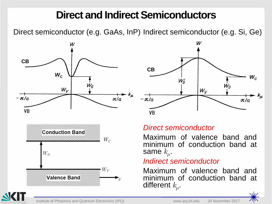
Direct and Indirect Semiconductors
Direct semiconductor (e.g. GaAs, InP) Indirect semiconductor (e.g. Si, Ge)
Direct semiconductor
Maximum of valence band andminimum of conduction band atsame kµ.Indirect semiconductor
Maximum of valence band andminimum of conduction band atdifferent kµ.
CB
CB
WCWC
CB
WC
Institute of Photonics and Quantum Electronics (IPQ) www.ipq.kit.edu 24 November 2017
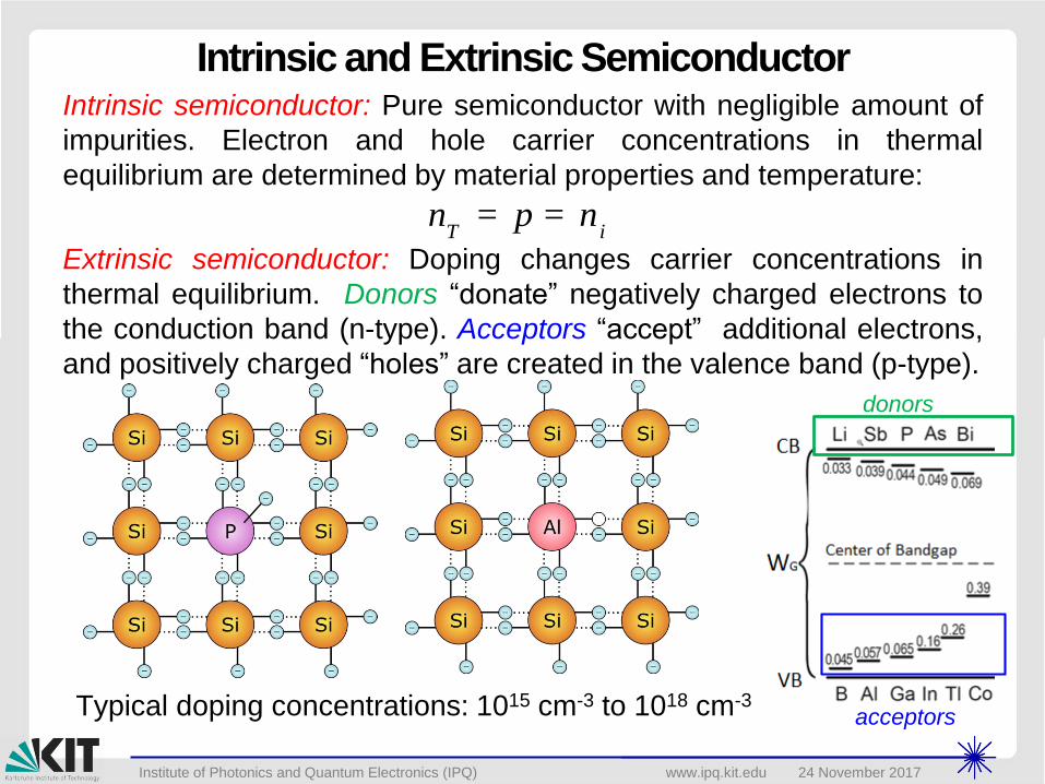
Intrinsic and Extrinsic SemiconductorIntrinsic semiconductor: Pure semiconductor with negligible amount of
impurities. Electron and hole carrier concentrations in thermal
equilibrium are determined by material properties and temperature:
Extrinsic semiconductor: Doping changes carrier concentrations in
thermal equilibrium. Donors “donate” negatively charged electrons to
the conduction band (n-type). Acceptors “accept” additional electrons,
and positively charged “holes” are created in the valence band (p-type).
T in p n= =
donors
acceptorsTypical doping concentrations: 1015 cm-3 to 1018 cm-3
Institute of Photonics and Quantum Electronics (IPQ) www.ipq.kit.edu 24 November 2017
Intrinsic and Extrinsic SemiconductorIntrinsic semiconductor: Pure semiconductor with negligible amount of
impurities. Electron and hole carrier concentrations in thermal
equilibrium are determined by material properties and temperature:
Extrinsic semiconductor: Doping changes carrier concentrations in
thermal equilibrium. Donors “donate” negatively charged electrons to
the conduction band (n-type). Acceptors “accept” additional electrons,
and positively charged “holes” are created in the valence band (p-type).
2
T in p n=
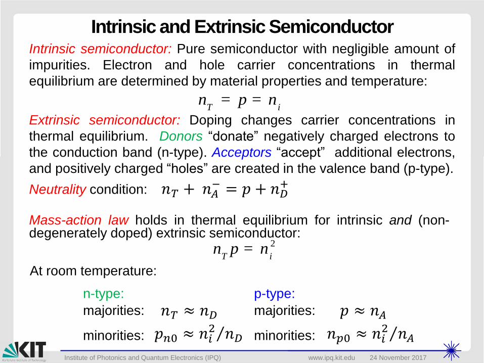
Mass-action law holds in thermal equilibrium for intrinsic and (non-degenerately doped) extrinsic semiconductor:
Neutrality condition:
T in p n= =
𝑛𝑇 + 𝑛𝐴− = 𝑝 + 𝑛𝐷
+
n-type: p-type:
majorities: majorities:
minorities: minorities:
𝑛𝑇 ≈ 𝑛𝐷 𝑝 ≈ 𝑛𝐴𝑝𝑛0 ≈ Τ𝑛𝑖
2 𝑛𝐷 𝑛𝑝0 ≈ Τ𝑛𝑖2 𝑛𝐴
At room temperature:
Institute of Photonics and Quantum Electronics (IPQ) www.ipq.kit.edu 24 November 2017
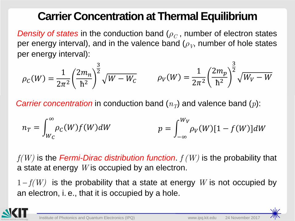
Carrier Concentration at Thermal Equilibrium
Density of states in the conduction band (rC , number of electron states
per energy interval), and in the valence band (rV, number of hole states
per energy interval):
Carrier concentration in conduction band (nT) and valence band (p):
f(W) is the Fermi-Dirac distribution function. f (W) is the probability that
a state at energy W is occupied by an electron.
1 f(W) is the probability that a state at energy W is not occupied by
an electron, i. e., that it is occupied by a hole.
𝜌𝐶 𝑊 =1
2𝜋22𝑚𝑛
ħ2
32
𝑊 −𝑊𝐶𝜌𝑉 𝑊 =
1
2𝜋22𝑚𝑝
ħ2
32
𝑊𝑉 −𝑊
𝑛𝑇 = න𝑊𝐶
∞
𝜌𝐶 𝑊 𝑓 𝑊 𝑑𝑊 𝑝 = න−∞
𝑊𝑉
𝜌𝑉 𝑊 [1 − 𝑓 𝑊 ]𝑑𝑊
Institute of Photonics and Quantum Electronics (IPQ) www.ipq.kit.edu 24 November 2017
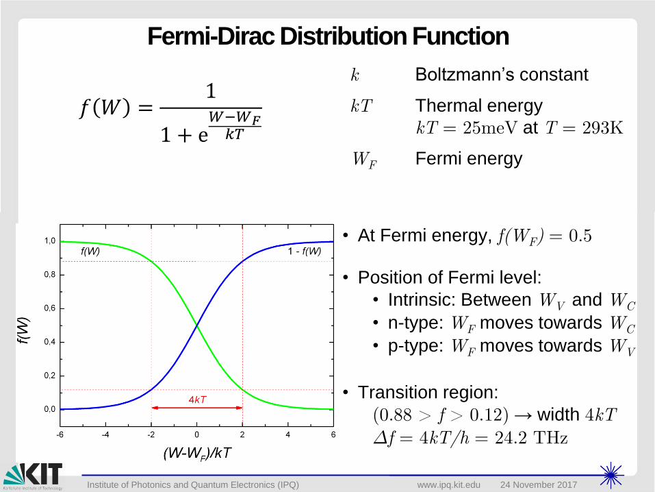
Fermi-Dirac Distribution Function
k Boltzmann’s constant
kT Thermal energy
kT = 25meV at T = 293K
WF Fermi energy
• At Fermi energy, f(WF) = 0.5
• Position of Fermi level:
• Intrinsic: Between WV and WC
• n-type: WF moves towards WC
• p-type: WF moves towards WV
• Transition region:
(0.88 > f > 0.12) → width 4kTDf = 4kT/h = 24.2 THz
𝑓 𝑊 =1
1 + ⅇ𝑊−𝑊𝐹𝑘𝑇
Institute of Photonics and Quantum Electronics (IPQ) www.ipq.kit.edu 24 November 2017
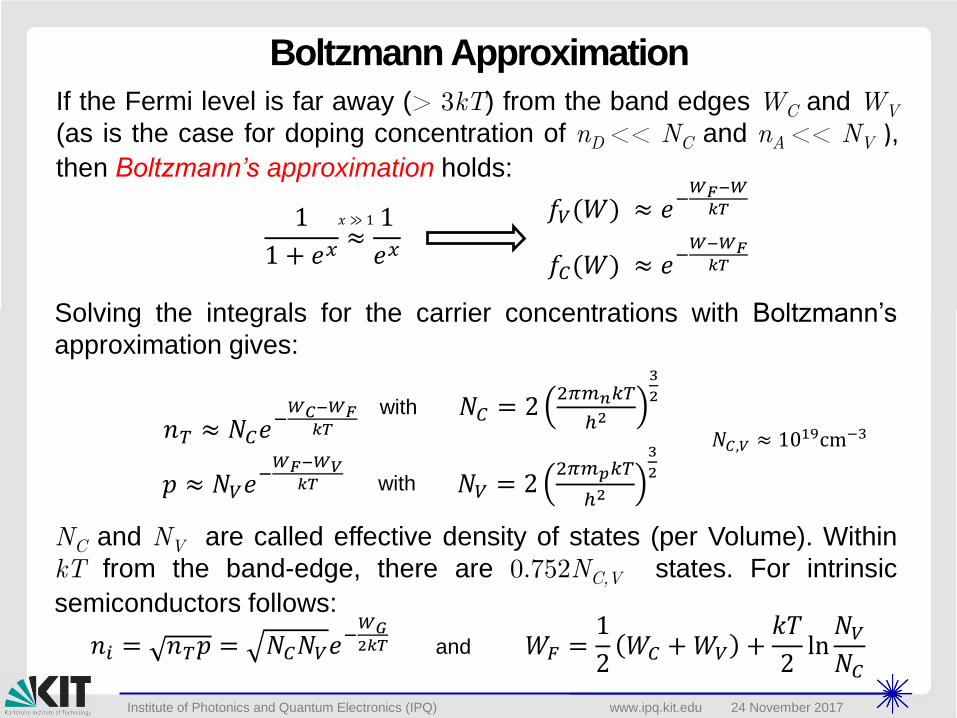
Boltzmann Approximation
If the Fermi level is far away (> 3kT) from the band edges WC and WV
(as is the case for doping concentration of nD << NC and nA << NV ),
then Boltzmann’s approximation holds:
Solving the integrals for the carrier concentrations with Boltzmann’s
approximation gives:
NC and NV are called effective density of states (per Volume). Within
kT from the band-edge, there are 0.752NC,V states. For intrinsic
semiconductors follows:
1
1 + 𝑒𝑥≈
1
𝑒𝑥𝑥 ≫ 1 𝑓𝑉(𝑊) ≈ 𝑒−
𝑊𝐹−𝑊
𝑘𝑇
𝑓𝐶(𝑊) ≈ 𝑒−𝑊−𝑊𝐹𝑘𝑇
𝑛𝑖 = 𝑛𝑇𝑝 = 𝑁𝐶𝑁𝑉𝑒−𝑊𝐺2𝑘𝑇
𝑁𝐶 = 22𝜋𝑚𝑛𝑘𝑇
ℎ2
3
2with
𝑝 ≈ 𝑁𝑉𝑒−𝑊𝐹−𝑊𝑉
𝑘𝑇 𝑁𝑉 = 22𝜋𝑚𝑝𝑘𝑇
ℎ2
3
2with
𝑁𝐶,𝑉 ≈ 1019cm−3𝑛𝑇 ≈ 𝑁𝐶𝑒−𝑊𝐶−𝑊𝐹
𝑘𝑇
𝑊𝐹 =1
2𝑊𝐶 +𝑊𝑉 +
𝑘𝑇
2ln𝑁𝑉𝑁𝐶
and
Institute of Photonics and Quantum Electronics (IPQ) www.ipq.kit.edu 24 November 2017
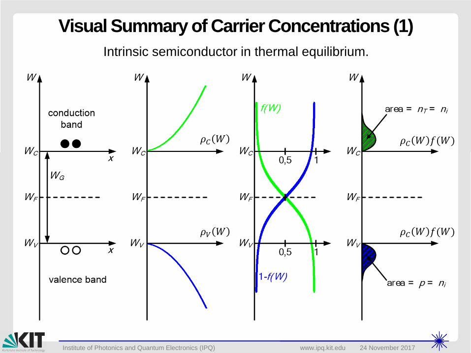
Visual Summary of Carrier Concentrations (1)
Intrinsic semiconductor in thermal equilibrium.
𝜌𝐶 𝑊
𝜌𝑉 𝑊
𝜌𝐶 𝑊 𝑓(𝑊)
𝜌𝐶 𝑊 𝑓(𝑊)
Institute of Photonics and Quantum Electronics (IPQ) www.ipq.kit.edu 24 November 2017
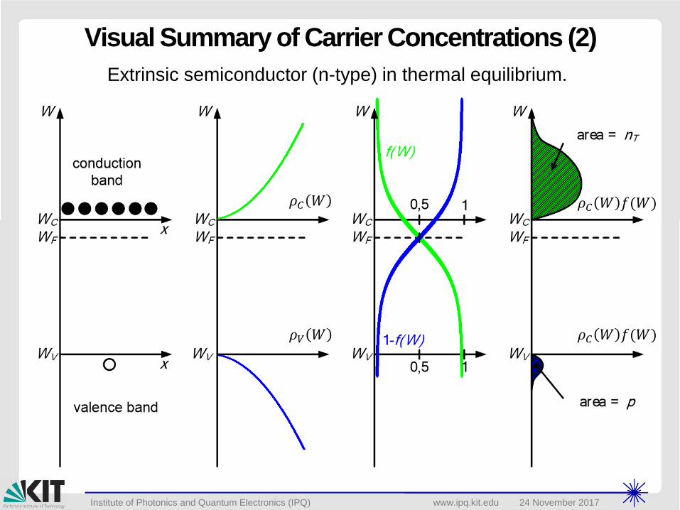
Visual Summary of Carrier Concentrations (2)
Extrinsic semiconductor (n-type) in thermal equilibrium.
𝜌𝐶 𝑊
𝜌𝑉 𝑊
𝜌𝐶 𝑊 𝑓(𝑊)
𝜌𝐶 𝑊 𝑓(𝑊)
Institute of Photonics and Quantum Electronics (IPQ) www.ipq.kit.edu 24 November 2017
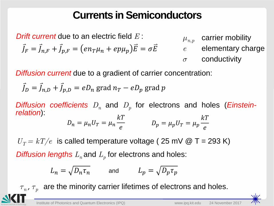
Currents in Semiconductors
Drift current due to an electric field E : mn,p carrier mobility
e elementary charge
s conductivity
Diffusion current due to a gradient of carrier concentration:
Diffusion coefficients Dn and Dp for electrons and holes (Einstein-relation):
Diffusion lengths Ln and Lp for electrons and holes:
tn , tp are the minority carrier lifetimes of electrons and holes.
റ𝐽𝐹 = റ𝐽𝑛,𝐹 + റ𝐽𝑝,𝐹 = 𝑒𝑛𝑇𝜇𝑛 + 𝑒𝑝𝜇𝑝 𝐸 = 𝜎𝐸
റ𝐽𝐷 = റ𝐽𝑛,𝐷 + റ𝐽𝑝,𝐷 = 𝑒𝐷𝑛 grad 𝑛𝑇 − 𝑒𝐷𝑝 grad 𝑝
𝐿𝑛 = 𝐷𝑛𝜏𝑛 𝐿𝑝 = 𝐷𝑝𝜏𝑝and
𝐷𝑛 = 𝜇𝑛𝑈𝑇 = 𝜇𝑛𝑘𝑇
𝑒𝐷𝑝 = 𝜇𝑝𝑈𝑇 = 𝜇𝑝
𝑘𝑇
𝑒
UT = kT/e is called temperature voltage ( 25 mV @ T = 293 K)
Institute of Photonics and Quantum Electronics (IPQ) www.ipq.kit.edu 24 November 2017
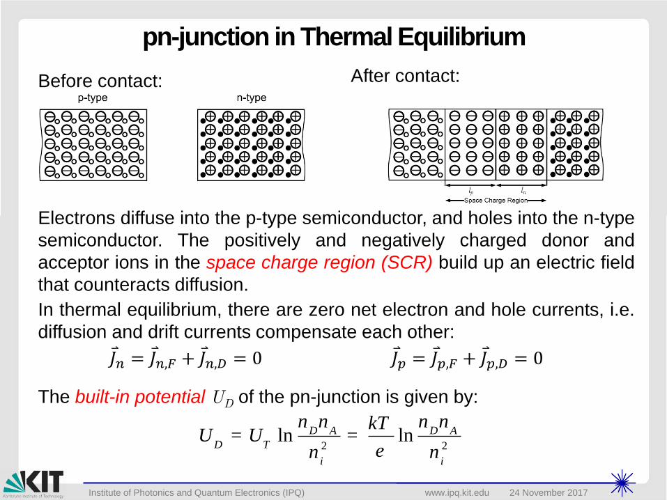
pn-junction in Thermal Equilibrium
Electrons diffuse into the p-type semiconductor, and holes into the n-type
semiconductor. The positively and negatively charged donor and
acceptor ions in the space charge region (SCR) build up an electric field
that counteracts diffusion.
In thermal equilibrium, there are zero net electron and hole currents, i.e.
diffusion and drift currents compensate each other:
Before contact: After contact:
The built-in potential UD of the pn-junction is given by:
2 2ln lnD A D A
D T
i i
n n n nkTU U
en n= =
റ𝐽𝑝 = റ𝐽𝑝,𝐹 + റ𝐽𝑝,𝐷 = 0റ𝐽𝑛 = റ𝐽𝑛,𝐹 + റ𝐽𝑛,𝐷 = 0
Institute of Photonics and Quantum Electronics (IPQ) www.ipq.kit.edu 24 November 2017
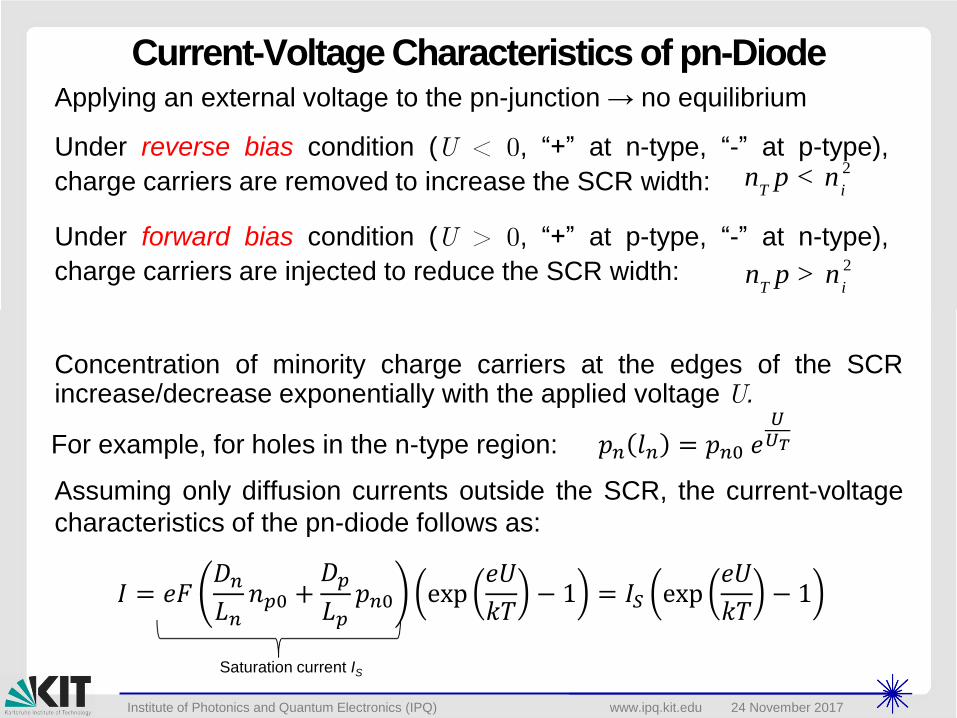
Current-Voltage Characteristics of pn-DiodeApplying an external voltage to the pn-junction → no equilibrium
2
T in p n>
2
T in p n<
Under reverse bias condition (U < 0, “+” at n-type, “-” at p-type),
charge carriers are removed to increase the SCR width:
Under forward bias condition (U > 0, “+” at p-type, “-” at n-type),
charge carriers are injected to reduce the SCR width:
Assuming only diffusion currents outside the SCR, the current-voltage
characteristics of the pn-diode follows as:
Concentration of minority charge carriers at the edges of the SCRincrease/decrease exponentially with the applied voltage U.
𝑝𝑛 𝑙𝑛 = 𝑝𝑛0 𝑒𝑈𝑈𝑇
𝐼 = 𝑒𝐹𝐷𝑛𝐿𝑛
𝑛𝑝0 +𝐷𝑝
𝐿𝑝𝑝𝑛0 ⅇxp
𝑒𝑈
𝑘𝑇− 1 = 𝐼𝑆 ⅇxp
𝑒𝑈
𝑘𝑇− 1
Saturation current IS
For example, for holes in the n-type region:
Institute of Photonics and Quantum Electronics (IPQ) www.ipq.kit.edu 24 November 2017
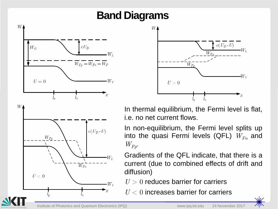
Band Diagrams
In thermal equilibrium, the Fermi level is flat,
i.e. no net current flows.
In non-equilibrium, the Fermi level splits upinto the quasi Fermi levels (QFL) WFn and
WFp.
Gradients of the QFL indicate, that there is a
current (due to combined effects of drift and
diffusion)
U > 0 reduces barrier for carriers
U < 0 increases barrier for carriers
Institute of Photonics and Quantum Electronics (IPQ) www.ipq.kit.edu 24 November 2017
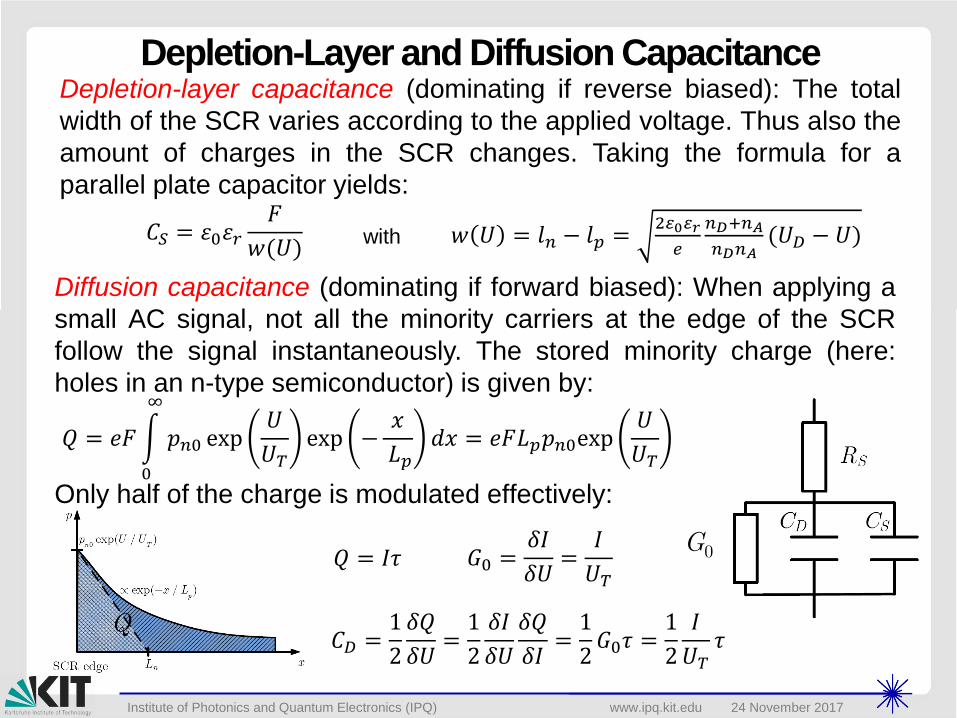
Depletion-Layer and Diffusion CapacitanceDepletion-layer capacitance (dominating if reverse biased): The total
width of the SCR varies according to the applied voltage. Thus also the
amount of charges in the SCR changes. Taking the formula for a
parallel plate capacitor yields:
Only half of the charge is modulated effectively:
Diffusion capacitance (dominating if forward biased): When applying a
small AC signal, not all the minority carriers at the edge of the SCR
follow the signal instantaneously. The stored minority charge (here:
holes in an n-type semiconductor) is given by:
G0
𝐶𝑆 = 휀0휀𝑟𝐹
𝑤(𝑈)𝑤 𝑈 = 𝑙𝑛 − 𝑙𝑝 =
2𝜀0𝜀𝑟
𝑒
𝑛𝐷+𝑛𝐴
𝑛𝐷𝑛𝐴(𝑈𝐷 − 𝑈)with
𝑄 = 𝑒𝐹න
0
∞
𝑝𝑛0 ⅇxp𝑈
𝑈𝑇ⅇxp −
𝑥
𝐿𝑝𝑑𝑥 = 𝑒𝐹𝐿𝑝𝑝𝑛0ⅇxp
𝑈
𝑈𝑇
𝑄 = 𝐼𝜏 𝐺0 =𝛿𝐼
𝛿𝑈=
𝐼
𝑈𝑇
𝐶𝐷 =1
2
𝛿𝑄
𝛿𝑈=1
2
𝛿𝐼
𝛿𝑈
𝛿𝑄
𝛿𝐼=1
2𝐺0𝜏 =
1
2
𝐼
𝑈𝑇𝜏


![Abstract arXiv:1610.04787v1 [cs.CV] 15 Oct 2016 · Ziad Al-Halah Makarand Tapaswi Rainer Stiefelhagen Karlsruhe Institute of Technology, 76131 Karlsruhe, Germany fziad.al-halah, makarand.tapaswi,](https://img.pdfslide.net/doc/110x75/5f5ddde74407be578927c733/abstract-arxiv161004787v1-cscv-15-oct-2016-ziad-al-halah-makarand-tapaswi-rainer.jpg)