Embed Size (px)
Citation preview

Quality requirements for wafers, cells and PV modules
Stefan Krauter, Paul Grunow, Sven LehmannPI Photovoltaik-Institut Berlin AGPhotovoltaic Module TechnologyTesting | Consulting | Research
Intersolar 2008 in Munich, 12th of June 2008
Out
door
test
-site
PI B
erlin
cells & wafersabout PI Berlin modules thin film modules
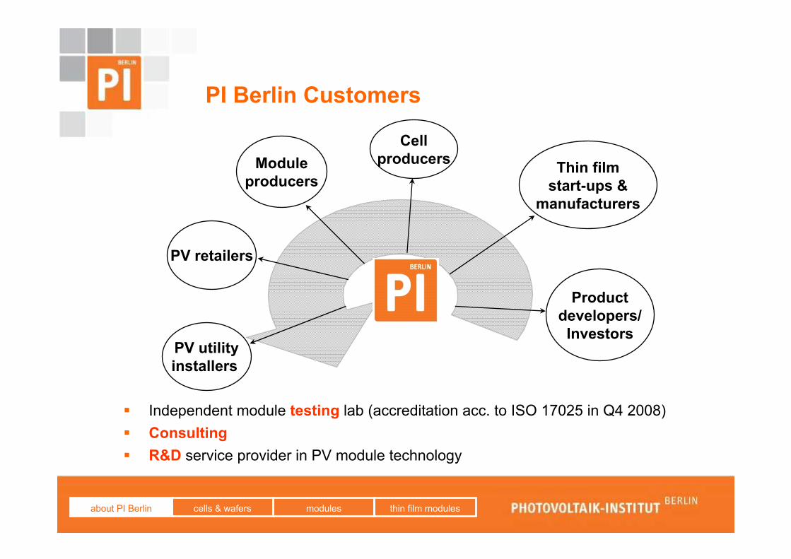
Independent module testing lab (accreditation acc. to ISO 17025 in Q4 2008) Consulting R&D service provider in PV module technology
Thin filmstart-ups &
manufacturers
PV utilityinstallers
Moduleproducers
Cellproducers
Productdevelopers/Investors
PV retailers
PI Berlin Customers
cells & wafersabout PI Berlin modules thin film modules

PI Berlin: PV Module testing and R&D services
Testing equipment Class A Flasher for STC precision measurements + weak light performance 3 climate chambers 2.8m x 3.0m x 2.6m (damp-heat, thermal cycling, humidity-freeze) Steady state simulator class B (STC for thin film modules, hot spot, light soaking) Outdoor test-site: NOCT, yield comparison, max. 40 modules UV chamber, area: 2.0m x 3.6m x 2.0m Wet leakage electrical isolation test (up to 6000 V) Mechanical tests (load, hail, rip-off) Accelerated TCO corrosion tests EVA gel content test
Equipment for Research and Development Module lamination service:
Edge delete, contacting, lamination IR-thermography, Electroluminescence Spectral response measurement Fig.1: Outdoor test site in Berlin
4 founders in October 2006, 20 employees in June 2008
cells & wafersabout PI Berlin modules thin film modules

Characterisation in PV manufacturing
• Yield improvement = average efficiency x mechanical yield
• Continuous throughput increase• Raw material supplier feed-back• Safety & reliability and energy yield check (module)
Prominent example:
Expected benefits:
• Cell or module binning in power classes ->mismatch reduction in the module or in the system
e.g. Field&Gabor 29th IEEE PVSC, New Orleans 2002, p. 418
cells & wafersabout PI Berlin modules thin film modules

Which characterisation tools make it from the laboratory into the production?
• Fast: ≈ 1s • Reliable and easy to interpret• Relevance of revealed parameters• Invest vs. potential yield improvements
Investment and its return for the prominent example:
Needs:
• Cell sorting in 0.2% steps for cells between 14%-17% with a sorter at 3% of total invest*→ ≈ + 3% in average module power**
*=0.3 Mio € for a 30MW/a cell +module, ** = +2 Mio €/a -> i.e. already 0.1% yield improvement pays off the same invest
cells & wafersabout PI Berlin modules thin film modules

Wafer production
Crystallization
Ingot cutting
Wafer cutting
Sorting
poly-Silicon
Wafer
Cleaning
μ-PCD life timeIR spectroscopy
Visual inspection,balance: dimensions,mechanical defects
Resistivity, e.g.eddy current
No electronic quality check,no micro-crack inspectionat the final product!
Resistivity, e.g.eddy current
Silicon specification:Impurity contentsOxygen/carbon contents
cells & wafersabout PI Berlin modules thin film modules

Cell production
Wet etch
Diffusion
Wet deoxidation& edge isolation
Screen printing
wafer
SiNix ARC
Sheet resistivity
I-V curve: Iop@Vop*Pmax, Isc, Voc, FF,
Rseries, Rshunt
Visual:mechanical defects,
dimensions
Visual:colour
Firing
Sorting cell
Visual
Wafer specification:ResistivityDopantDimensions, geometryMechanical defectsImpurity/oxygen contentMinimum carrier life time
Feedback to wafer supplier:Electronic qualityMechanical quality
cells & wafersabout PI Berlin modules thin film modules
*Vop= 0.5 V as sorting criteria

New fast characterization of single wafers
Photoluminescence Imaging using a self-consistent calibration method as introducedby T. Trupke et al., Applied Physics Letter, Vol 87, 184 (2005)
-> Cell efficiency prediction on the wafer level in terms of the cell‘s potential Isc,To do for as-cut wafers: Measurement in HF or iodine solution, corona charging??
cells & wafersabout PI Berlin modules thin film modules
The et al. 22nd EPVSEC 2007, Milan, p. 354

Photoluminescence Imaging of raw wafers
BruchrisikoIn-Line Messungen Elektrolumineszenz Photolumineszenz
-> without passivation (such as cut):out-sorting of (EFG) wafers with low minority carrier lifetime possible
Trupke et al. 22nd EPVSEC 2007, Milan, p. 22

Micro crack inspection of wafers
Trupke et al. 22nd EPVSEC 2007, Milan, p. 22
Photoluminescence ImagingHistory of luminescence Imaging:
2005: T. Fuyuki, et al., Applied Physics Letters 86 (26) (2005) p. 262108
2007: >20 papers at the 22nd PVSEC in Milano related to electro- and photo-luminescence on wafers, cells and modules
Remark: older papers exists about photo emission microscopy (PEM) for failure analysis in microelectronics
cells & wafersabout PI Berlin modules thin film modules

Electroluminescence on finished cells (modules)
cells & wafersabout PI Berlin modules thin film modules
Finger interruptionscracks
Vacuum suction cups (zoom) Firing furnace belt(zoom)
local shunts(artificial, by wire connect back to front)

Hot spot risk test on cells
after D. Schüren from Sunware, private communication 2005* = cycle time
Infrared Imaging at -10V
W. Herrmann et al. 17th EPVSEC, Munich, 2001
Test criteria: Maximum temperature after 1s* < Tcritical
cells & wafersabout PI Berlin modules thin film modules

Cell production+
Wet etching
Diffusion
Wet de-oxidation & edge isolation
Screen printing
wafer
SiNx ARC
Sheet resistivity
I-V curve: Iop@Vop
Pmax, Isc, Voc, FF,Rseries, Rshunt
Visual check:mechanical defects,
dimensions
Visual check:colour
Firing
Sorting
EL camera • Finger interruptions,• Homogeneity,• Micro-cracks,• Local shunts
IR camera Hot spots
PL cameraFeedback to wafer supplier:Electronic qualityMechanical quality
cell
Visual check
cells & wafersabout PI Berlin modules thin film modules
Wafer specifications:• Resistivity• Dopant• Dimensions, geometry• Mechanical defects• Impurity/oxygen content• Minimum carrier life time
PL
PL
PL
PL
PL
Micro-crack alarm-system along the entire production process& software tool for visualisation of micro-crack attraction points

Module production
String soldering
Matrix soldering
Lamination
Sun Simulator test
Cell
Module
J-box & Framing
String testerPmax, Rseries
I-V-curve: Pmax, Isc, Voc, FF,
Rseries, Rshunt
EL camera
PL cameraFeedback to cell supplier:Electronic qualityMechanical quality
EL camera Stringer check
EL camera Check before laminationCell specification:• I@Vop• Pmax• Dimensions, geometry• Mechanical defects
low light I-V-curve: Pmax at 100-400 W/m2
Energy yield issue
cells & wafersabout PI Berlin modules thin film modules
Final check

Elektroluminescence on finished modules
- Local shunts- Finger
interruptions
- areas with low diffusion length
-Micro cracks
cells & wafersabout PI Berlin modules thin film modules

Thin Film module production
Deposition & Patterning
Edge deletion
Contacting
Sun Simulator test
Glass
TF Module / Laminate
J-box (& Framing)I-V-curve:
Pmax, Isc, Voc, FF,Rseries, Rshunt
Lamination
Visual: Laserpattern alignment
Insulation test
EL/PL camera
EL camera
Insulation test Safety issue
low light I-V-curve:Pmax at 100-400 W/m2
Energy yield issue
Voc check
cells & wafersabout PI Berlin modules thin film modules

Electroluminescence on thin film modules
CIGS: with several local defects/shuntsa-Si/μ-Si
-> fast detection/imaging of local material defects or processing faults
CdTe
local shunt
local shunt
badedgedelete
cells & wafersabout PI Berlin modules thin film modules

Yield of module prediction via operation model
Standard Test Conditions (STC)PV module power output at 25°C1,000 W/m2, AM 1.5g, normal incidenceTypical measurement duration: 4-10 ms
Real world is non-STC!Indoor test ≠ outdoor performance• Non-perpendicular incidence• Low irradiance levels• Spectral effects• Temperature effects • Degradation and regeneration
Electrical energy yield (kWh/a kWp)is predictable for crystalline technologies,but more difficult for thin film technologies(degradation, change of parameters)

Conclusions
• 0.1% yield improvement justifies an invest of 0.3 Mio€ in a 30 MW combined c-Si cell&module line at today’s pricings
• Electro- and photoluminescence are powerful tools for fast in-line imaging of electronic and mechanical properties on wafers, cells and modules, minimum yield improvement: 1%
• Hereby, the highest benefit is expected for micro crack detection, especially for highly automated production lines
• Since CCD cameras are used, they can be combined with/ or replace conventional visual inspection stations
• Safety risks (i.e., hot spot and isolation) and energy yieldpotential of the finished modules are important product properties in the field and should to be covered with similar investment efforts (recommended product strategy)
• Hall B6, 410
[email protected]@pi-berlin.comVielen Dank