Embed Size (px)
Citation preview

Overview of ICAMR -
International Consortium for
Advanced Manufacturing Research
1
Florida Photonics Cluster MeetingDecember 8, 2016
Teresa Pace, PhD
Industry
•Emerging Technologies
•Manufacturing
•Commercialization
Universities
•Universities in U.S.,
Europe, and Asia
•Funded research
•New ideas and approaches
•Partnered research capabilities
Government
• International
• State of Florida
• National research labs and agencies
• Attract joint funds
Suppliers
•Equipment
•Materials
•Software
• Industry R&D Labs & Programs
Innovation Networks & Open Innovation Programs That
Bring Industry, Universities And Governments Together
ICAMR: A New Era of International Collaboration

University/Lab Research
CONCEPT:
Creative Ideas
Centers of Excellence
Novel Techniques &
innovative technologies
Fundamental Research
Intelligence
ICAMR INTEGRATION: Accelerate high potential technologies into
next generation products & systems
ICAMR and partners develop and provide
commercialization infrastructure
Capability for proof of concept, custom
development, pilot production
IP Protection
COMMERCIALIZATION:
Integration of advanced silicon
based devices
Sensors & Photonics
Nanotechnologies
Biomedical devices/products
NEMS / MEMS
Emerging technologies
3-D Integration / Packaging
Advanced Imagers & Lasers
Integrated Systems
Industry
Open Innovation PlatformNavigate Path from Concept to Commercialization
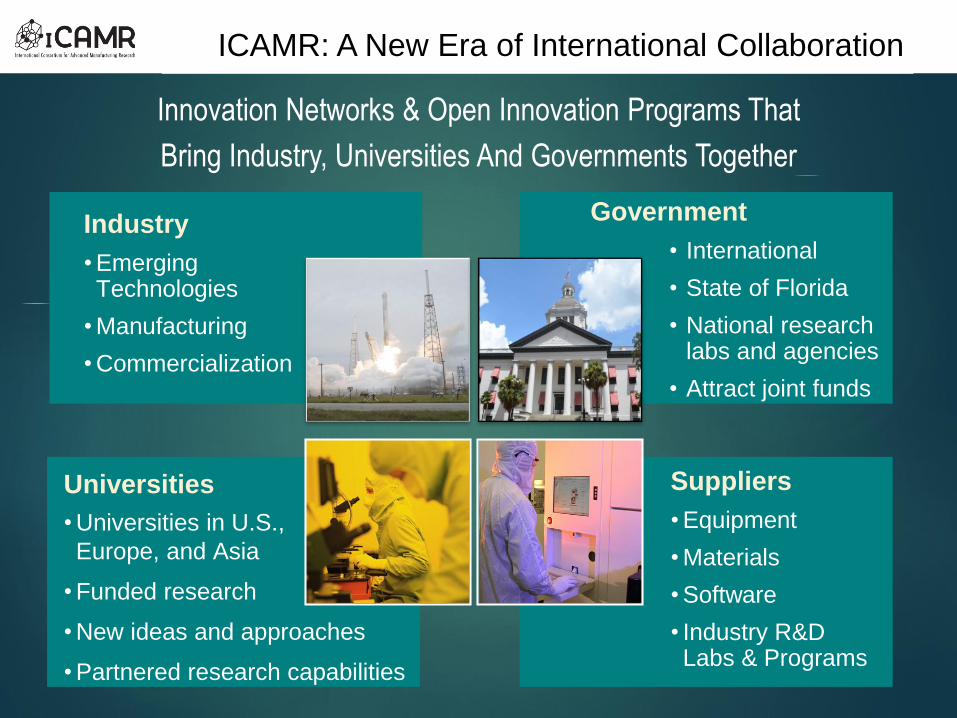
Smart Sensors
Built-in computational resources to process data and present it in a more accurate, efficient, and informative way
Includes ‘intelligence’ in the equation
Next disruptive market explosion will be ‘semiconductor-based’ connected devices – led by advanced
sensors and complimentary photonic devices
Smart Sensors
UV sensors detect
skin cancer in the
shower
IR/LADAR imagers -
Advanced Driver
Assistance Systems
(ADAS)
Hyperspectral
Imagers – Detect crop
safety and stresses
Multiband Imagers
detect intruders,
immediately alert first
responders
Improve productivity, efficiency, and overall quality of life
Microfluidic sensors
- Perspiration to detect
diabetic attack
Bio/Chem sensors
detect food spoilage
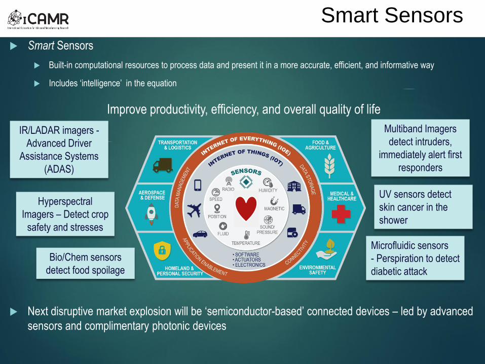
IoT and IoE
IoT
Network of physical objects or “things” (devices, webcams, phones, vehicles, buildings, and toys) embedded with electronics, software, sensors, that are connected in order to collect and exchange data
99.4% physical objects are still unconnected
Vulnerable to security attacks, malicious intent
IoE
Incorporates people, processing, data, connectivity, and applications
Transfer, storage, and interpretation of massive amounts of data
Includes the analysis required to turn data information into actionable information
Business value creation has shifted to power of connections and to ability to create intelligence from them
Must include security 5
Rapid Financial
Growth of IoE,
IoT, Sensors
Improving Performance, Efficiency, and People’s Lives
2024 2026 2028 2030
Internet of Things
Imagers and Chem/Bio Sensors
$50B
$15T
$200B
$800B
$28B
$20T
$35T
$500B

• Provide smart sensor semi-conductor technology solutions and
pilot-line production
• Integration of smart sensors, imagers, and photonic devices on CMOS leveraging
2.5/3D integration - SoC & SiP
• Emphasis on novel materials (i.e. III-V) on Si
• Manufacturing scale-up of III-V materials and next generation smart sensors⁻ Faster performance at lower power, wide band gap, high voltage and frequency stability, chemical and extreme
environment robustness
⁻ Development of High Volume manufacturing processes, equipment, supply chain for transition to
• Pilot-line for Low Volume / High Mix / High Value products
• Addressing and providing solutions to array of challenges in embedded security,
anti-tamper and anti-counterfeit for new and legacy systems
• Partnered with imec FL’s System and Design Center to develop
advanced sensors, imagers, photonics, and optics
• Other local industry partners include: PhotonX, Tupperware,
Aurora Semi, and Harris
ICAMR Role In IoT/IoE
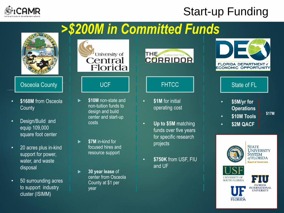
• $168M from Osceola
County
• Design/Build and
equip 109,000
square foot center
• 20 acres plus in-kind
support for power,
water, and waste
disposal
• 50 surrounding acres
to support industry
cluster (ISIMM)
$10M non-state and non-tuition funds to design and build center and start-up costs
$7M in-kind for focused hires and resource support
30 year lease of center from Osceola County at $1 per year
• $1M for initial
operating cost
• Up to $5M matching
funds over five years
for specific research
projects
• $750K from USF, FIU
and UF
• $5M/yr for
Operations
• $10M Tools
• $2M QACF
Osceola County UCF FHTCC State of FL
>$200M in Committed Funds
$17M
Start-up Funding
95
75
10
4
95
75
PensacolaJacksonville
Orlando
Tampa
Miami
Kissimmee
Cape CanaveralSanford
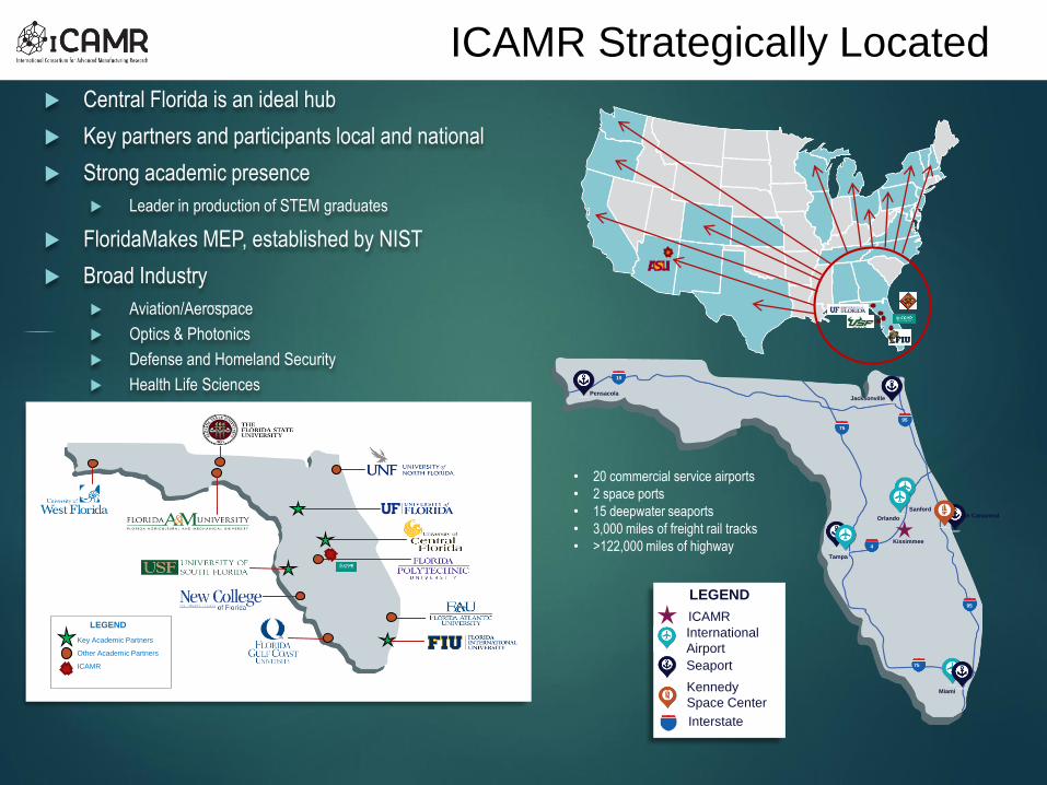
Central Florida is an ideal hub
Key partners and participants local and national
Strong academic presence
Leader in production of STEM graduates
FloridaMakes MEP, established by NIST
Broad Industry
Aviation/Aerospace
Optics & Photonics
Defense and Homeland Security
Health Life Sciences
Key Academic Partners
Other Academic Partners
ICAMR
LEGEND
• 20 commercial service airports
• 2 space ports
• 15 deepwater seaports
• 3,000 miles of freight rail tracks
• >122,000 miles of highway
LEGEND
ICAMR
International
Airport
Seaport
Kennedy
Space Center
Interstate
ICAMR Strategically Located
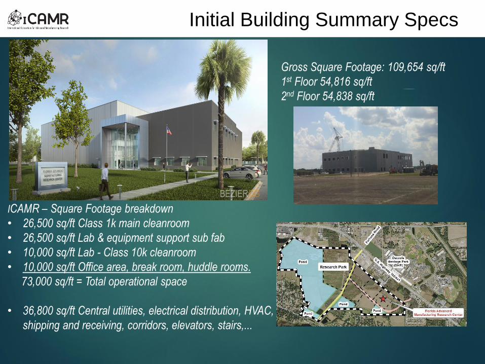
ICAMR – Square Footage breakdown
• 26,500 sq/ft Class 1k main cleanroom
• 26,500 sq/ft Lab & equipment support sub fab
• 10,000 sq/ft Lab - Class 10k cleanroom
• 10,000 sq/ft Office area, break room, huddle rooms.
73,000 sq/ft = Total operational space
• 36,800 sq/ft Central utilities, electrical distribution, HVAC,
shipping and receiving, corridors, elevators, stairs,...
Gross Square Footage: 109,654 sq/ft
1st Floor 54,816 sq/ft
2nd Floor 54,838 sq/ft
Initial Building Summary Specs

NIST Open Topic MII Funding Opportunity
Mission: Establish a domestic industrial-led Manufacturing Innovation Institute (MII) for the
design, manufacture, testing, assembly, and packaging for novel materials for transformational
sensors and imagers that addresses common manufacturing challenges across the entire
integrated sensor ecosystem.
Federal Objective: Bring government, industry and academia together with the goal of
organizing the current fragmented domestic capabilities in sensor and imager materials
technology and better position the U.S. relative to global competition.
Contracting Agency: Department of Commerce / NIST FFO 2016-NIST-NNMI-01
Federal Funding (cooperative agreement): $70 million over 5 years
Cost Matching Required: Min 1:1
Business Model: Industry Led Consortium Institute, Self sustaining by year 6
Full Proposal Submitted: July 22, 2016
Site Visit/Presentation: Sept 19-Oct 4, 2016
NIST Followup Questions: Nov 2016
Proposal Award/Funding: Q1, 2017
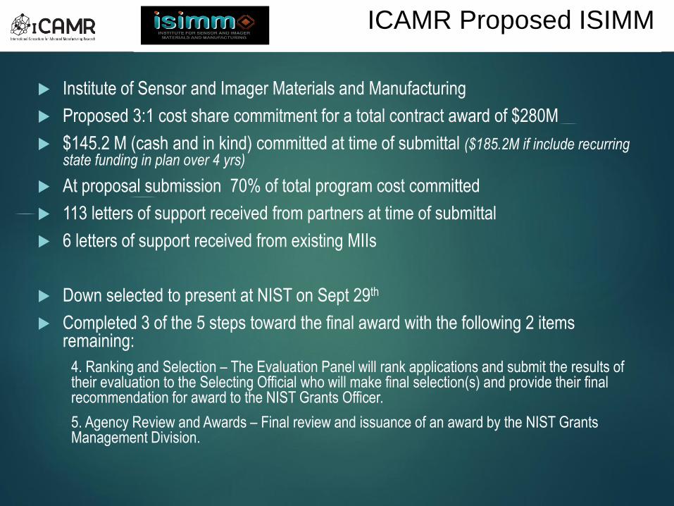
Institute of Sensor and Imager Materials and Manufacturing
Proposed 3:1 cost share commitment for a total contract award of $280M
$145.2 M (cash and in kind) committed at time of submittal ($185.2M if include recurring state funding in plan over 4 yrs)
At proposal submission 70% of total program cost committed
113 letters of support received from partners at time of submittal
6 letters of support received from existing MIIs
Down selected to present at NIST on Sept 29th
Completed 3 of the 5 steps toward the final award with the following 2 items remaining:
4. Ranking and Selection – The Evaluation Panel will rank applications and submit the results of their evaluation to the Selecting Official who will make final selection(s) and provide their final recommendation for award to the NIST Grants Officer.
5. Agency Review and Awards – Final review and issuance of an award by the NIST Grants Management Division.
ICAMR Proposed ISIMM
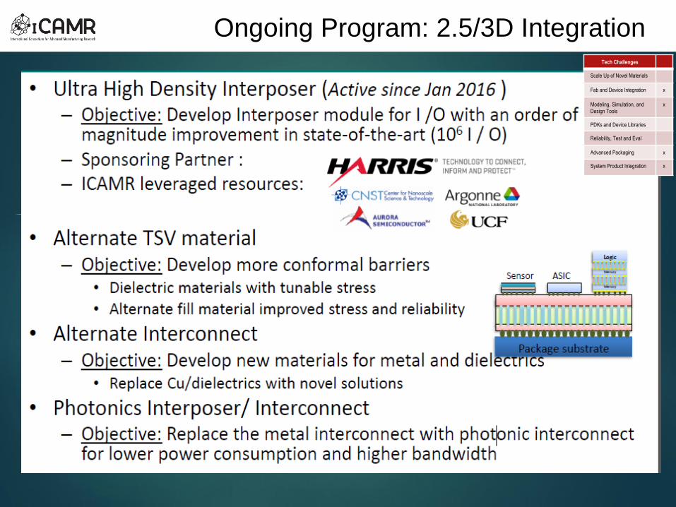
Ongoing Program: 2.5/3D IntegrationTech Challenges
Scale Up of Novel Materials
Fab and Device Integration x
Modeling, Simulation, and
Design Tools
x
PDKs and Device Libraries
Reliability, Test and Eval
Advanced Packaging x
System Product Integration x
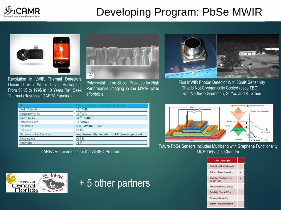
First MWIR Photon Detector With 35mK Sensitivity
That Is Not Cryogenically Cooled (uses TEC).
Ref: Northrop Grumman, S. Yoo and K. Green
Revolution in LWIR Thermal Detectors
Occurred with Wafer Level Packaging.
From 50K$ to 199$ in 10 Years Ref: Seek
Thermal (Results of DARPA Funding)
Future PbSe Sensors Includes Multiband with Graphene Functionality
UCF: Debashis ChandraDARPA Requirements for the WIRED Program
Polycrystalline on Silicon Provides for High
Performance Imaging in the MWIR while
affordable
Developing Program: PbSe MWIR
Tech Challenges
Scale Up of Novel Materials
Fab and Device Integration x
Modeling, Simulation, and
Design Tools
x
PDKs and Device Libraries
Reliability, Test and Eval
Advanced Packaging
System Product Integration
+ 5 other partners
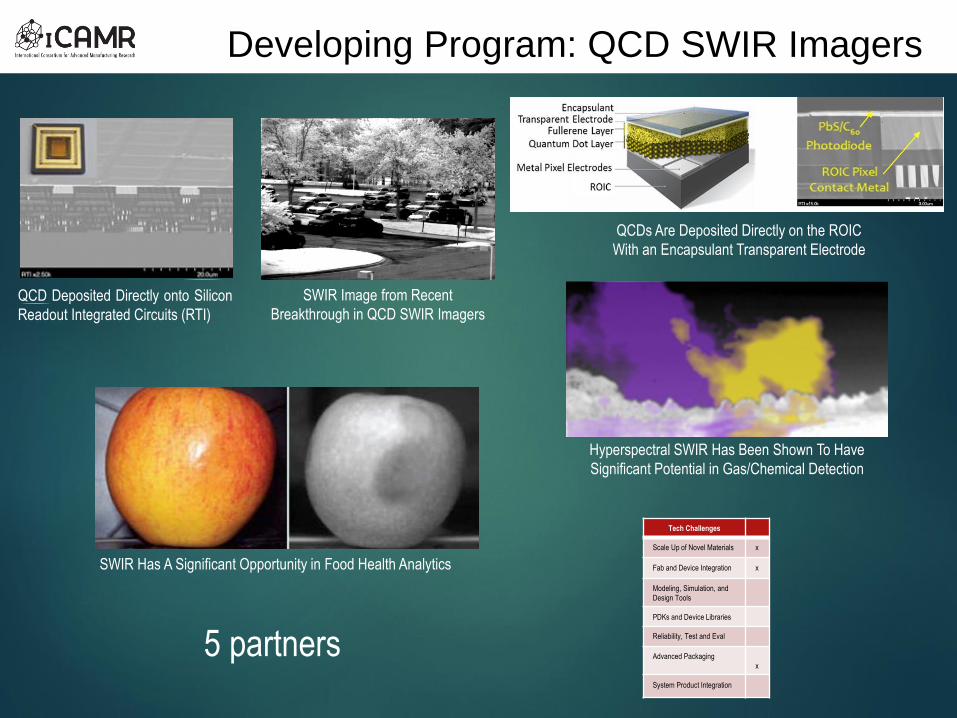
QCDs Are Deposited Directly on the ROIC
With an Encapsulant Transparent Electrode
QCD Deposited Directly onto Silicon
Readout Integrated Circuits (RTI)
Hyperspectral SWIR Has Been Shown To Have
Significant Potential in Gas/Chemical Detection
SWIR Has A Significant Opportunity in Food Health Analytics
SWIR Image from Recent
Breakthrough in QCD SWIR Imagers
Tech Challenges
Scale Up of Novel Materials x
Fab and Device Integration x
Modeling, Simulation, and
Design Tools
PDKs and Device Libraries
Reliability, Test and Eval
Advanced Packaging
x
System Product Integration
5 partners
Developing Program: QCD SWIR Imagers

Gallium Nitride (GaN)-based High Electron Mobility Transistors
(HEMT)s have been shown to be a viable solution for a myriad
of chemical and biological sensing applications (e.g., gases,
toxins, cancers, biomarkers such as glucose, heavy metals,
and marine pathogens
Schematic for Protein Detection with High
Electron Mobility Transistors (HEMT)
Developing Program: GaN Medical Sensors
+ 4 other partners
Tech Challenges
Scale Up of Novel Materials
Fab and Device Integration x
Modeling, Simulation, and
Design Tools
PDKs and Device Libraries
Reliability, Test and Eval x
Advanced Packaging
x
System Product Integration
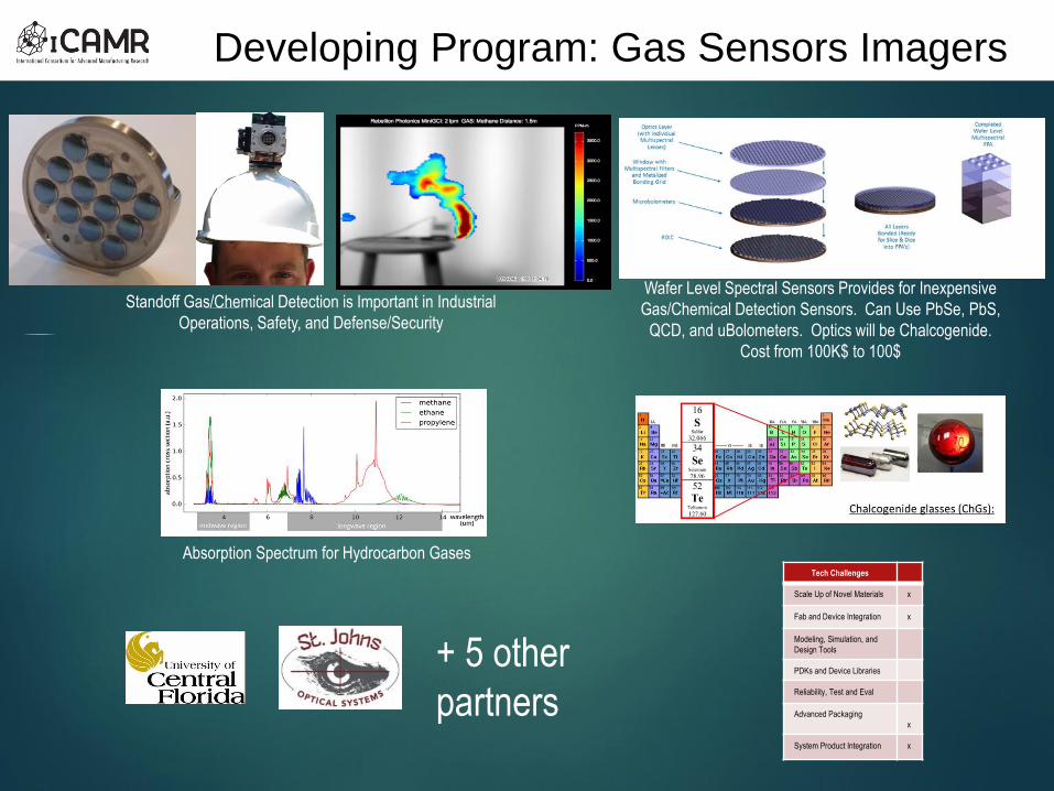
Standoff Gas/Chemical Detection is Important in Industrial
Operations, Safety, and Defense/Security
Wafer Level Spectral Sensors Provides for Inexpensive
Gas/Chemical Detection Sensors. Can Use PbSe, PbS,
QCD, and uBolometers. Optics will be Chalcogenide.
Cost from 100K$ to 100$
Absorption Spectrum for Hydrocarbon Gases
+ 5 other
partners
Tech Challenges
Scale Up of Novel Materials x
Fab and Device Integration x
Modeling, Simulation, and
Design Tools
PDKs and Device Libraries
Reliability, Test and Eval
Advanced Packaging
x
System Product Integration x
Developing Program: Gas Sensors Imagers
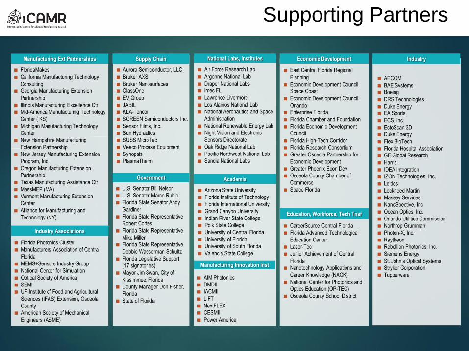
AECOM
BAE Systems
Boeing
DRS Technologies
Duke Energy
EA Sports
ECS, Inc.
EctoScan 3D
Duke Energy
Flex BioTech
Florida Hospital Association
GE Global Research
Harris
IDEA Integration
IZON Technologies, Inc.
Leidos
Lockheed Martin
Massey Services
NanoSpective, Inc
Ocean Optics, Inc.
Orlando Utilities Commission
Northrop Grumman
Photon-X, Inc.
Raytheon
Rebellion Photonics, Inc.
Siemens Energy
St. John’s Optical Systems
Stryker Corporation
Tupperware
National Labs, Institutes
Academia
CareerSource Central Florida
Florida Advanced Technological
Education Center
Laser-Tec
Junior Achievement of Central
Florida
Nanotechnology Applications and
Career Knowledge (NACK)
National Center for Photonics and
Optics Education (OP-TEC)
Osceola County School District
Economic Development
East Central Florida Regional
Planning
Economic Development Council,
Space Coast
Economic Development Council,
Orlando
Enterprise Florida
Florida Chamber and Foundation
Florida Economic Development
Council
Florida High-Tech Corridor
Florida Research Consortium
Greater Osceola Partnership for
Economic Development
Greater Phoenix Econ Dev
Osceola County Chamber of
Commerce
Space Florida
Industry
Air Force Research Lab
Argonne National Lab
Draper National Labs
imec FL
Lawrence Livermore
Los Alamos National Lab
National Aeronautics and Space
Administration
National Renewable Energy Lab
Night Vision and Electronic
Sensors Directorate
Oak Ridge National Lab
Pacific Northwest National Lab
Sandia National Labs
Education, Workforce, Tech Tnsf
Arizona State University
Florida Institute of Technology
Florida International University
Grand Canyon University
Indian River State College
Polk State College
University of Central Florida
University of Florida
University of South Florida
Valencia State College
Government
U.S. Senator Bill Nelson
U.S. Senator Marco Rubio
Florida State Senator Andy
Gardiner
Florida State Representative
Robert Cortes
Florida State Representative
Mike Miller
Florida State Representative
Debbie Wasserman Schultz
Florida Legislative Support
(17 signatories)
Mayor Jim Swan, City of
Kissimmee, Florida
County Manager Don Fisher,
Florida
State of Florida
Aurora Semiconductor, LLC
Bruker AXS
Bruker Nanosurfaces
ClassOne
EV Group
JABIL
KLA-Tencor
SCREEN Semiconductors Inc.
Sensor Films, Inc.
Sun Hydraulics
SUSS MicroTec
Veeco Process Equipment
Synopsis
PlasmaTherm
Supply Chain
FloridaMakes
California Manufacturing Technology
Consulting
Georgia Manufacturing Extension
Partnership
Illinois Manufacturing Excellence Ctr
Mid-America Manufacturing Technology
Center ( KS)
Michigan Manufacturing Technology
Center
New Hampshire Manufacturing
Extension Partnership
New Jersey Manufacturing Extension
Program, Inc.
Oregon Manufacturing Extension
Partnership
Texas Manufacturing Assistance Ctr
MassMEP (MA)
Vermont Manufacturing Extension
Center
Alliance for Manufacturing and
Technology (NY)
Florida Photonics Cluster
Manufacturers Association of Central
Florida
MEMS+Sensors Industry Group
National Center for Simulation
Optical Society of America
SEMI
UF-Institute of Food and Agricultural
Sciences (IFAS) Extension, Osceola
County
American Society of Mechanical
Engineers (ASME)
Manufacturing Ext Partnerships
Industry Associations
AIM Photonics
DMDII
IACMII
LIFT
NextFLEX
CESMII
Power America
1 National Need, Impacts,
and Broad Benefits
Manufacturing Innovation Inst
Supporting Partners
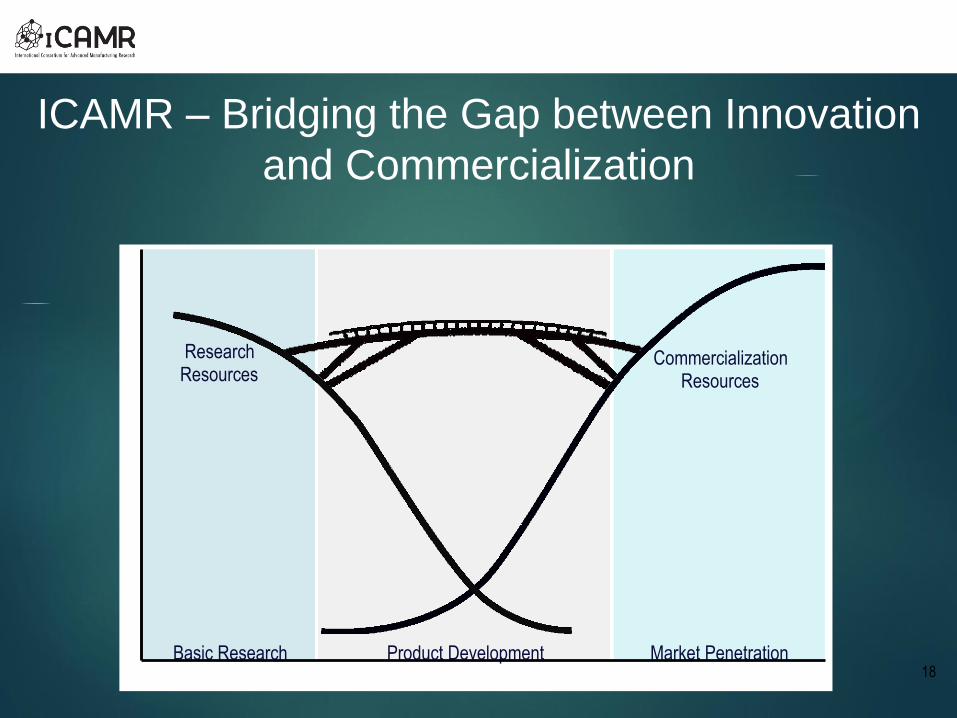
ICAMR – Bridging the Gap between Innovation
and Commercialization
18Basic Research Market PenetrationProduct Development
Commercialization Resources
Research Resources
CONTACT
ICAMR - 407-742-4254
400 W. Emmett Street
Kissimmee, FL 34741
19www.icamr.net