Embed Size (px)
Citation preview
March 6th 2013 www.thonk.co.uk 1
258J PCB component Kit
258J PCB component kit Instructions
Version 1.3.1
OVERVIEW Please provide feedback on this document via email - [email protected] You should read this entire document first before building the 258J kit. This document provides key information for building the 258J Oscillator component kit as available from Thonk. These notes are not written for complete beginners but a more detailed build document will follow eventually. This BOM will work with any revision of the J3RK 258J board, however the images in this document are specific to the boards which are marked REV 1-28-2013. Older PCB revisions did not have revisions marked and some required modification to work correctly. Refer to the thread linked below to determine which board you have – In particular there was a run of boards in late 2012 which required a trace being cut and a jumper wire adding – http://www.muffwiggler.com/forum/viewtopic.php?t=66072&start=142 DOCUMENT HISTORY v1.0 – March 6th 2013 v1.1 – May 19th 2013
• Wiring diagram now specific to Clarke68 euro panel • Ground output was titled incorrectly in the ʻTest Wiringʼ section
v1.2 – May 28th 2013
• Full Eurorack kit construction, powering and wiring instructions • Buffering for Eurorack level outputs
v1.3 – July 14th 2013
• Better testing documentation • Continuity testing information • Improved switch wiring instructions • Trimming guidelines
March 6th 2013 www.thonk.co.uk 2
258J PCB component Kit
258J PCB component kit Instructions
Version 1.3.1
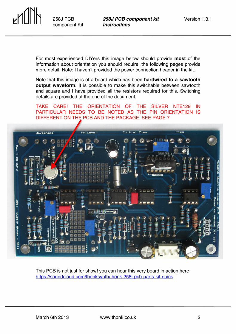
For most experienced DIYers this image below should provide most of the information about orientation you should require, the following pages provide more detail. Note: I havenʼt provided the power connection header in the kit.
Note that this image is of a board which has been hardwired to a sawtooth output waveform. It is possible to make this switchable between sawtooth and square and I have provided all the resistors required for this. Switching details are provided at the end of the document.
TAKE CARE! THE ORIENTATION OF THE SILVER NTE129 IN PARTICULAR NEEDS TO BE NOTED AS THE PIN ORIENTATION IS DIFFERENT ON THE PCB AND THE PACKAGE. SEE PAGE 7
This PCB is not just for show! you can hear this very board in action here https://soundcloud.com/thonksynth/thonk-258j-pcb-parts-kit-quick
March 6th 2013 www.thonk.co.uk 3
258J PCB component Kit
258J PCB component kit Instructions
Version 1.3.1
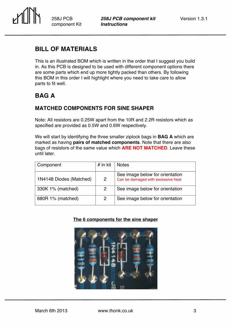
BILL OF MATERIALS This is an illustrated BOM which is written in the order that I suggest you build in. As this PCB is designed to be used with different component options there are some parts which end up more tightly packed than others. By following this BOM in this order I will highlight where you need to take care to allow parts to fit well. BAG A MATCHED COMPONENTS FOR SINE SHAPER Note: All resistors are 0.25W apart from the 10R and 2.2R resistors which as specified are provided as 0.5W and 0.6W respectively. We will start by identifying the three smaller ziplock bags in BAG A which are marked as having pairs of matched components. Note that there are also bags of resistors of the same value which ARE NOT MATCHED. Leave these until later. Component # in kit Notes
1N4148 Diodes (Matched) 2 See image below for orientation Can be damaged with excessive heat
330K 1% (matched) 2 See image below for orientation
680R 1% (matched) 2 See image below for orientation
The 6 components for the sine shaper
March 6th 2013 www.thonk.co.uk 4
258J PCB component Kit
258J PCB component kit Instructions
Version 1.3.1
RESISTORS FOR SWITCH AND OPTIONAL 150K RESISTOR You should next take the following bags are reserve one of each for the sawtooth/square selection which we will approach after everything else is done.
The other 150K resistor is optional and is concerned with the range of voltage required for the waveshape modulation input. In a Eurorack system for example installing this resistor will provide a good compatible modulation range. In other systems you may want to leave it out until you have tested if your CV modulation is working across the entire range. If you donʼt install it itʼs fine to leave this space on the PCB empty, it doesnʼt need a jumper wire. Then the following resistors are reserved entirely for the Sawtooth/Square selection – put them also to one side for now. Component # in kit Notes
2.2K 1 For SWITCH #4
470R 1 For SWITCH #4
Component # in kit Notes
150K 1% 2 INCLUDES 1 RESISTOR FOR SWITCH #0 AND ONE OPTIONAL RESISTOR
330K 1% 2 INCLUDES 1 RESISTOR FOR SWITCH #1 Make sure you leave enough room to seat the 1M trimmer.
680K 1% 3 INCLUDES 1 RESISTOR FOR SWITCH #2
820K 1% 2 INCLUDES 1 RESISTOR FOR SWITCH #3
March 6th 2013 www.thonk.co.uk 5
258J PCB component Kit
258J PCB component kit Instructions
Version 1.3.1
REMAINING RESISTORS The remaining resistors can all now be soldered to the positions as indicated on the PCB. Component # in kit Notes 1.5M 1% 1 390K 1% 1 180K 1% 1 100K 1% 6 68K 1% 2 33K 1% 1 15K 1% 4 10K 1% 4 Loose - not bagged
Take care to allow the 100pF capacitor to fit between the 10k resistor and IC sockets.
6.81K 1% 1 6.8K 1% 2 4.99K 1% 1 3.3K 1% 2 2.49K 1% 1 1.8K 1% 1 680R 1% 2 390R 1% 1 Take care to leave enough room for the 100R
trimmer 10R (0.5 Watt) 1 2.2R (0.6 Watt) 1 Bag is not marked as (0.6 Watt, but it is)
March 6th 2013 www.thonk.co.uk 6
258J PCB component Kit
258J PCB component kit Instructions
Version 1.3.1
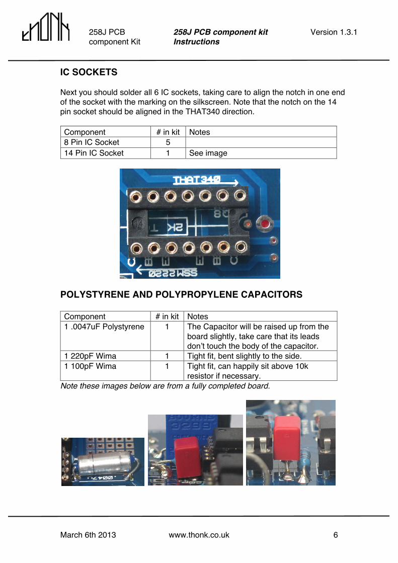
IC SOCKETS Next you should solder all 6 IC sockets, taking care to align the notch in one end of the socket with the marking on the silkscreen. Note that the notch on the 14 pin socket should be aligned in the THAT340 direction. Component # in kit Notes 8 Pin IC Socket 5 14 Pin IC Socket 1 See image
POLYSTYRENE AND POLYPROPYLENE CAPACITORS Component # in kit Notes 1 .0047uF Polystyrene 1 The Capacitor will be raised up from the
board slightly, take care that its leads donʼt touch the body of the capacitor.
1 220pF Wima 1 Tight fit, bent slightly to the side. 1 100pF Wima 1 Tight fit, can happily sit above 10k
resistor if necessary. Note these images below are from a fully completed board.
March 6th 2013 www.thonk.co.uk 7
258J PCB component Kit
258J PCB component kit Instructions
Version 1.3.1
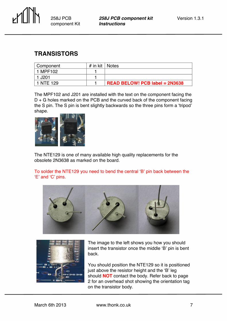
TRANSISTORS Component # in kit Notes 1 MPF102 1 1 J201 1 1 NTE 129 1 READ BELOW! PCB label = 2N3638
The MPF102 and J201 are installed with the text on the component facing the D + G holes marked on the PCB and the curved back of the component facing the S pin. The S pin is bent slightly backwards so the three pins form a ʻtripodʼ shape.
The NTE129 is one of many available high quality replacements for the obsolete 2N3638 as marked on the board. To solder the NTE129 you need to bend the central ʻBʼ pin back between the ʻEʼ and ʻCʼ pins.
The image to the left shows you how you should insert the transistor once the middle ʻBʼ pin is bent back. You should position the NTE129 so it is positioned just above the resistor height and the ʻBʼ leg should NOT contact the body. Refer back to page 2 for an overhead shot showing the orientation tag on the transistor body.
March 6th 2013 www.thonk.co.uk 8
258J PCB component Kit
258J PCB component kit Instructions
Version 1.3.1
TRIMMERS Next you can install the four blue Bourns trimmers. Look to the image on page 2 for suitable orientations. Component # in kit Notes 1 100K Trim 1 “W 104” marked on top 1 100R Trim 1 “W 101” marked on top 1 1M Trim 1 “W 105” marked on top 1 20K Trim 1 “W 203” marked on top
ELECTROLYTIC CAPACITORS Next you can install the three Electro Caps. Remember, the lead with the long lead goes to the hole marked + on the PCB. The negative side of the cap is marked with a contrasting thick coloured line on the body of the cap. Look to the image on page 2 for confirmation of orientation. NOTE: If you plan on using a shrouded power connector (not provided) you can solder the two 100uF Capacitors onto the other side of the board. The long lead should still go to the + pad. Component # in kit Notes 1 15uF Electrolytic 1 2 100uF Electrolytic 2
March 6th 2013 www.thonk.co.uk 9
258J PCB component Kit
258J PCB component kit Instructions
Version 1.3.1
March 6th 2013 www.thonk.co.uk 10
258J PCB component Kit
258J PCB component kit Instructions
Version 1.3.1
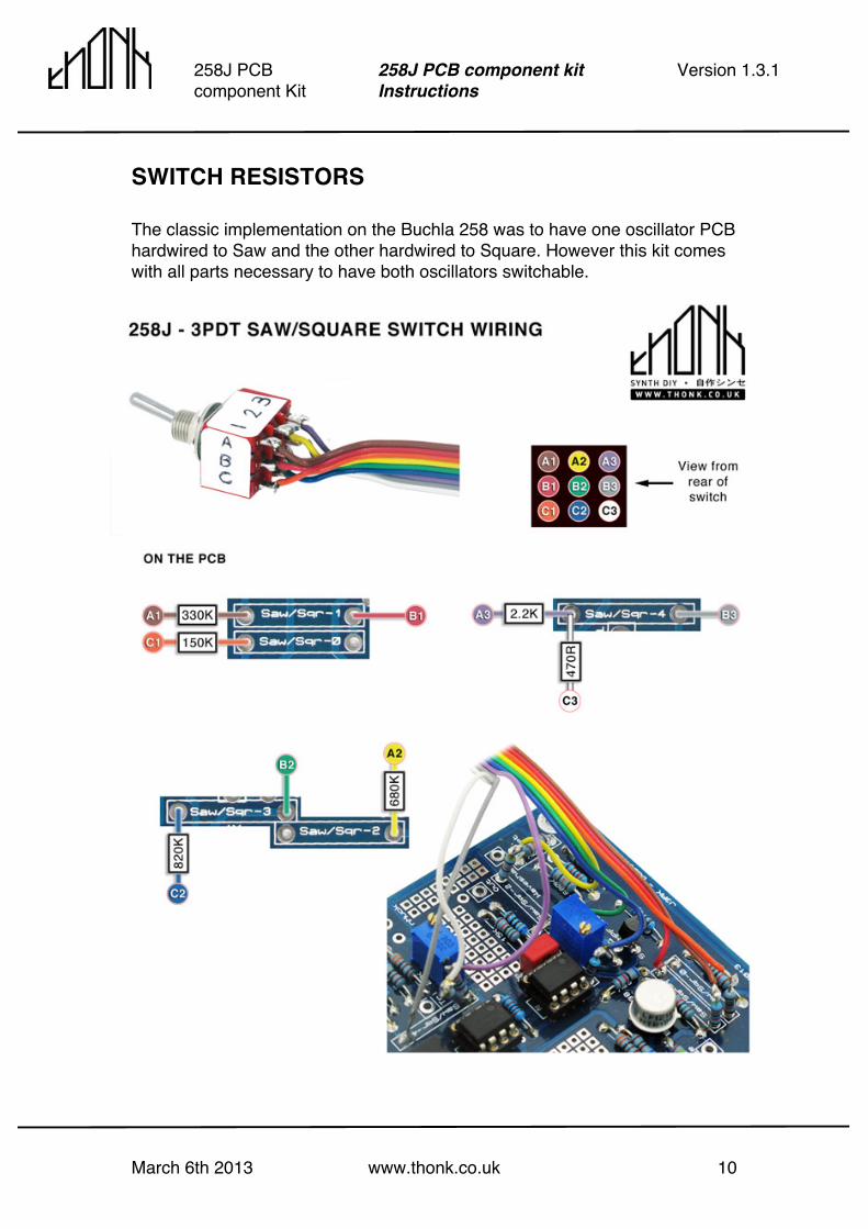
SWITCH RESISTORS The classic implementation on the Buchla 258 was to have one oscillator PCB hardwired to Saw and the other hardwired to Square. However this kit comes with all parts necessary to have both oscillators switchable.
March 6th 2013 www.thonk.co.uk 11
258J PCB component Kit
258J PCB component kit Instructions
Version 1.3.1
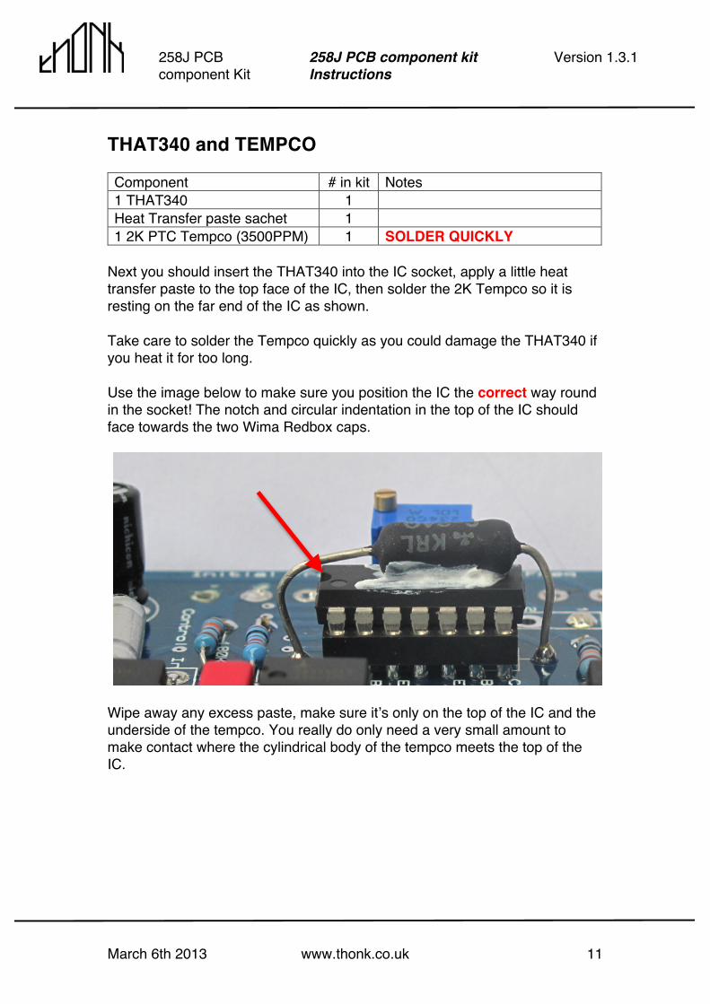
THAT340 and TEMPCO Component # in kit Notes 1 THAT340 1 Heat Transfer paste sachet 1 1 2K PTC Tempco (3500PPM) 1 SOLDER QUICKLY
Next you should insert the THAT340 into the IC socket, apply a little heat transfer paste to the top face of the IC, then solder the 2K Tempco so it is resting on the far end of the IC as shown. Take care to solder the Tempco quickly as you could damage the THAT340 if you heat it for too long. Use the image below to make sure you position the IC the correct way round in the socket! The notch and circular indentation in the top of the IC should face towards the two Wima Redbox caps.
Wipe away any excess paste, make sure itʼs only on the top of the IC and the underside of the tempco. You really do only need a very small amount to make contact where the cylindrical body of the tempco meets the top of the IC.
March 6th 2013 www.thonk.co.uk 12
258J PCB component Kit
258J PCB component kit Instructions
Version 1.3.1
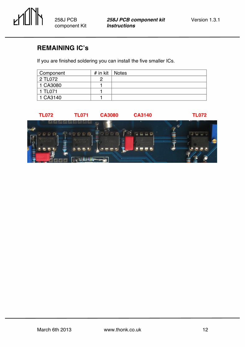
REMAINING ICʼs If you are finished soldering you can install the five smaller ICs. Component # in kit Notes 2 TL072 2 1 CA3080 1 1 TL071 1 1 CA3140 1
TL072 TL072 CA3140 CA3080 TL071
March 6th 2013 www.thonk.co.uk 13
258J PCB component Kit
258J PCB component kit Instructions
Version 1.3.1
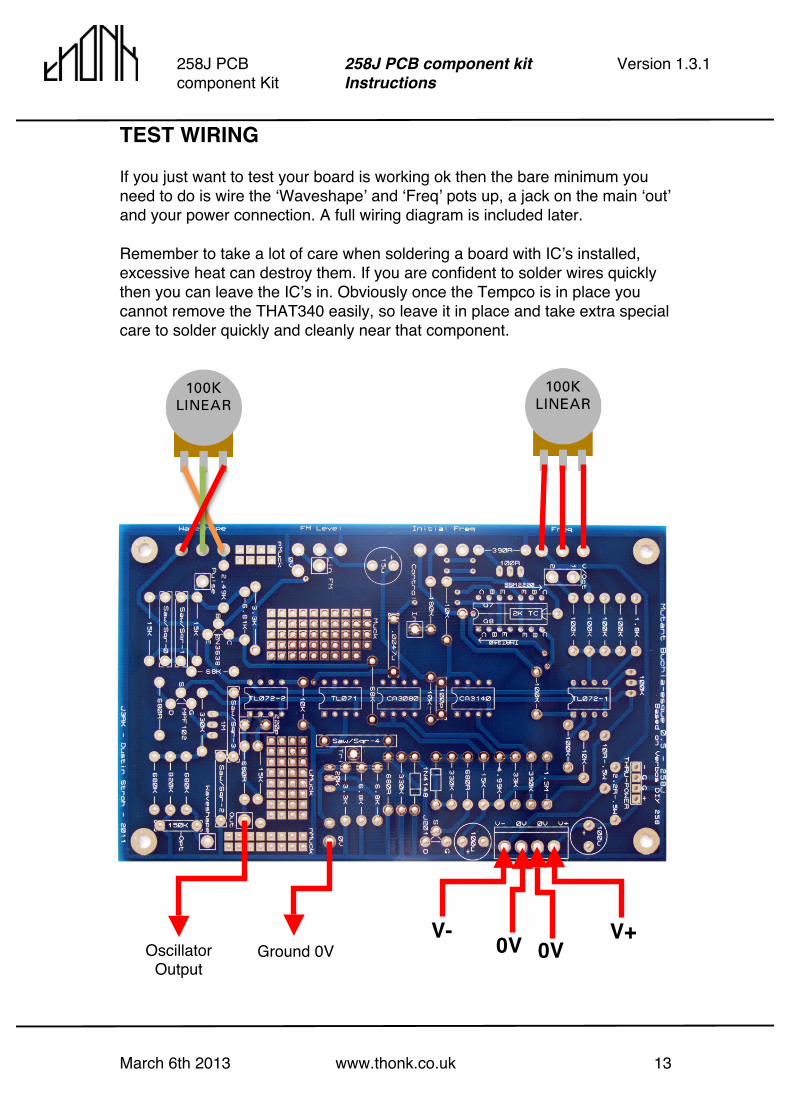
TEST WIRING If you just want to test your board is working ok then the bare minimum you need to do is wire the ʻWaveshapeʼ and ʻFreqʼ pots up, a jack on the main ʻoutʼ and your power connection. A full wiring diagram is included later. Remember to take a lot of care when soldering a board with ICʼs installed, excessive heat can destroy them. If you are confident to solder wires quickly then you can leave the ICʼs in. Obviously once the Tempco is in place you cannot remove the THAT340 easily, so leave it in place and take extra special care to solder quickly and cleanly near that component.
Oscillator Output
Signal / Tip
Ground 0V V- V+ 0V 0V
March 6th 2013 www.thonk.co.uk 14
258J PCB component Kit
258J PCB component kit Instructions
Version 1.3.1
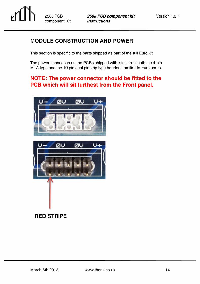
MODULE CONSTRUCTION AND POWER This section is specific to the parts shipped as part of the full Euro kit. The power connection on the PCBs shipped with kits can fit both the 4 pin MTA type and the 10 pin dual pinstrip type headers familiar to Euro users. NOTE: The power connector should be fitted to the PCB which will sit furthest from the Front panel.
RED STRIPE
March 6th 2013 www.thonk.co.uk 15
258J PCB component Kit
258J PCB component kit Instructions
Version 1.3.1
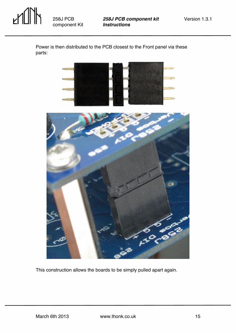
Power is then distributed to the PCB closest to the Front panel via these parts:
This construction allows the boards to be simply pulled apart again.
March 6th 2013 www.thonk.co.uk 16
258J PCB component Kit
258J PCB component kit Instructions
Version 1.3.1
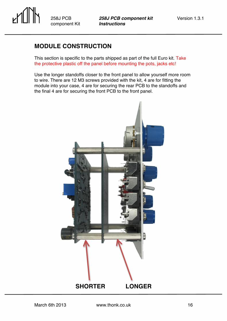
MODULE CONSTRUCTION This section is specific to the parts shipped as part of the full Euro kit. Take the protective plastic off the panel before mounting the pots, jacks etc! Use the longer standoffs closer to the front panel to allow yourself more room to wire. There are 12 M3 screws provided with the kit, 4 are for fitting the module into your case, 4 are for securing the rear PCB to the standoffs and the final 4 are for securing the front PCB to the front panel.
SHORTER LONGER
March 6th 2013 www.thonk.co.uk 17
258J PCB component Kit
258J PCB component kit Instructions
Version 1.3.1
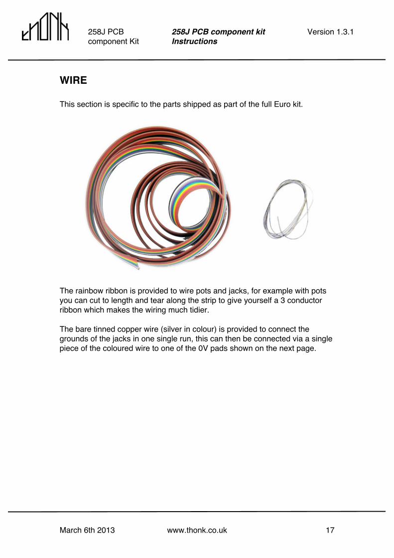
WIRE This section is specific to the parts shipped as part of the full Euro kit.
The rainbow ribbon is provided to wire pots and jacks, for example with pots you can cut to length and tear along the strip to give yourself a 3 conductor ribbon which makes the wiring much tidier. The bare tinned copper wire (silver in colour) is provided to connect the grounds of the jacks in one single run, this can then be connected via a single piece of the coloured wire to one of the 0V pads shown on the next page.
March 6th 2013 www.thonk.co.uk 18
258J PCB component Kit
258J PCB component kit Instructions
Version 1.3.1
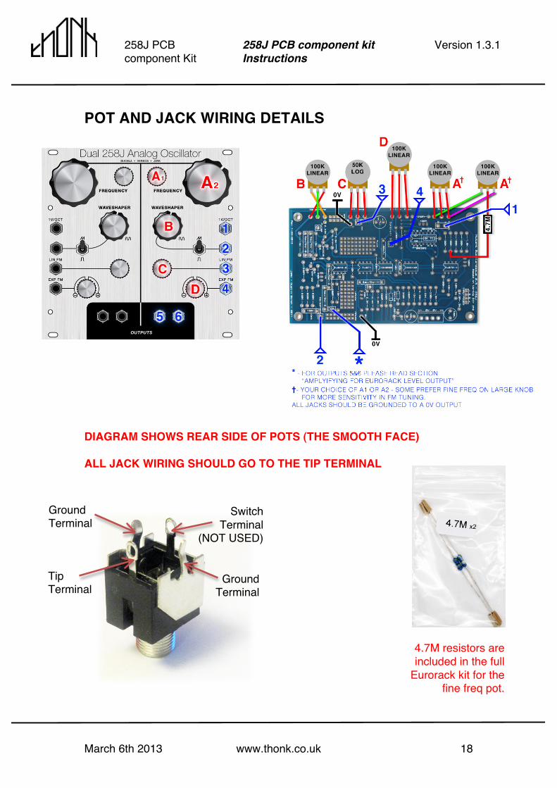
POT AND JACK WIRING DETAILS
DIAGRAM SHOWS REAR SIDE OF POTS (THE SMOOTH FACE) ALL JACK WIRING SHOULD GO TO THE TIP TERMINAL
Tip Terminal
Switch Terminal
(NOT USED)
Ground Terminal
Ground Terminal
4.7M resistors are included in the full
Eurorack kit for the fine freq pot.
March 6th 2013 www.thonk.co.uk 19
258J PCB component Kit
258J PCB component kit Instructions
Version 1.3.1
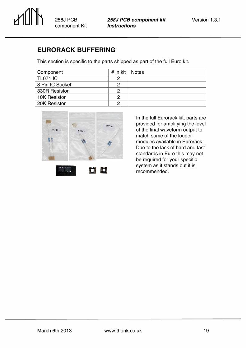
EURORACK BUFFERING This section is specific to the parts shipped as part of the full Euro kit. Component # in kit Notes TL071 IC 2 8 Pin IC Socket 2 330R Resistor 2 10K Resistor 2 20K Resistor 2
In the full Eurorack kit, parts are provided for amplifying the level of the final waveform output to match some of the louder modules available in Eurorack. Due to the lack of hard and fast standards in Euro this may not be required for your specific system as it stands but it is recommended.
March 6th 2013 www.thonk.co.uk 20
258J PCB component Kit
258J PCB component kit Instructions
Version 1.3.1
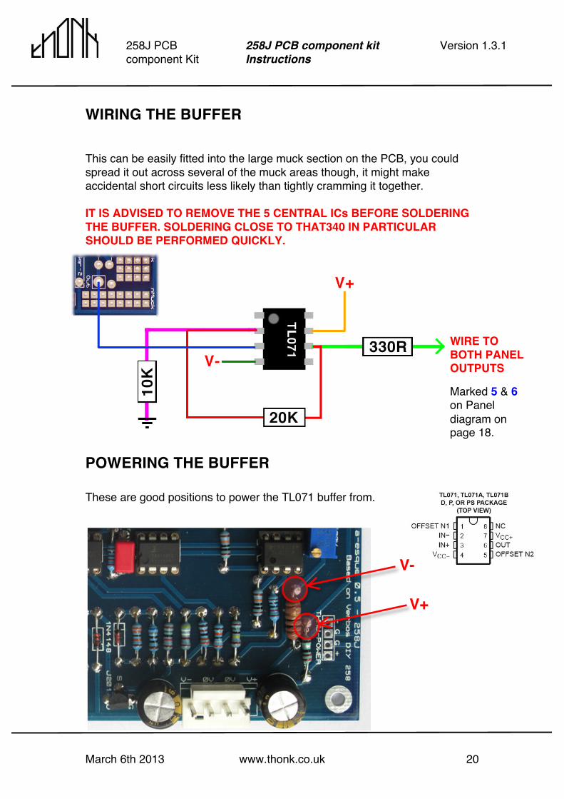
WIRING THE BUFFER
This can be easily fitted into the large muck section on the PCB, you could spread it out across several of the muck areas though, it might make accidental short circuits less likely than tightly cramming it together. IT IS ADVISED TO REMOVE THE 5 CENTRAL ICs BEFORE SOLDERING THE BUFFER. SOLDERING CLOSE TO THAT340 IN PARTICULAR SHOULD BE PERFORMED QUICKLY.
POWERING THE BUFFER These are good positions to power the TL071 buffer from.
V+
V-
WIRE TO BOTH PANEL OUTPUTS
Marked 5 & 6 on Panel diagram on page 18.

March 6th 2013 www.thonk.co.uk 21
258J PCB component Kit
258J PCB component kit Instructions
Version 1.3.1
TRIMMERS
100K Trim - Overall frequency range. 100R Trim - V/Oct Tracking 20K Trim - Sine shape 1M Trim – Waveshape fade
Here is how J3RK describes the trimming process to set the boards up.
I trim the 100K to taste by ear. Basically, I want it to extend both directions beyond my hearing range. (and then slightly more to the low end for doing semi-LFO duty) The 1M is to adjust the bias of the waveshape fading. I adjust it until it's more or less even across the range of the shape knob. I usually base it on the sine wave though, so I turn the panel knob fully to sine, and then trim from there. The 20K is to trim the sine wave. (you can also get some pretty interesting shapes by over-trimming this sometimes.) Then the last thing I do is trim the 1V/Oct.
SCHEMATIC For reference only - the original Mark Verbos schematic that the 258J is based on is here. http://www.simple-answer.com/258mod.jpg