Embed Size (px)
Citation preview

This is information on a product in full production.
June 2012 Doc ID 018687 Rev 3 1/40
1
STBP110
Overvoltage protection device
Datasheet - production data
Features■ Input overvoltage protection up to 28 V
■ Integrated high voltage N-channel MOSFET switch - low RDS(on) of 170 mΩ
■ Integrated charge pump
■ Maximum continuous current of 1.2 A
■ Thermal shutdown
■ Soft-start feature to control the inrush current
■ Enable input (EN)
■ Fault indication output (FLT)
■ IN input ESD protection: ±15 kV air discharge, ±8 kV contact discharge (with 1 µF input capacitor), ±2 kV HBM (standalone device)
■ Certain overvoltage options compliant with the China Communications Standard YD/T 1591-2006 (overvoltage protection only)
■ Small, RoHS compliant 2 x 2 x 0.75 mm TDFN 8-lead package with thermal pad.
Applications■ Smart phones
■ Digital cameras
■ PDA and palmtop devices
■ MP3 players
■ Low power handheld devices.
TDFN 8-lead (2 x 2 x 0.75 mm)
www.st.com

Contents STBP110
2/40 Doc ID 018687 Rev 3
Contents
1 Description . . . . . . . . . . . . . . . . . . . . . . . . . . . . . . . . . . . . . . . . . . . . . . . . . 6
2 Pin description . . . . . . . . . . . . . . . . . . . . . . . . . . . . . . . . . . . . . . . . . . . . . 7
2.1 Input (IN) . . . . . . . . . . . . . . . . . . . . . . . . . . . . . . . . . . . . . . . . . . . . . . . . . . 7
2.2 Output (OUT) . . . . . . . . . . . . . . . . . . . . . . . . . . . . . . . . . . . . . . . . . . . . . . . 7
2.3 Fault indication output (FLT) . . . . . . . . . . . . . . . . . . . . . . . . . . . . . . . . . . . . 7
2.4 Enable input (EN) . . . . . . . . . . . . . . . . . . . . . . . . . . . . . . . . . . . . . . . . . . . . 7
2.5 No connect (NC) . . . . . . . . . . . . . . . . . . . . . . . . . . . . . . . . . . . . . . . . . . . . . 8
2.6 Ground (GND) . . . . . . . . . . . . . . . . . . . . . . . . . . . . . . . . . . . . . . . . . . . . . . 8
3 Operation . . . . . . . . . . . . . . . . . . . . . . . . . . . . . . . . . . . . . . . . . . . . . . . . . 10
3.1 Power-up . . . . . . . . . . . . . . . . . . . . . . . . . . . . . . . . . . . . . . . . . . . . . . . . . 10
3.2 Normal operation . . . . . . . . . . . . . . . . . . . . . . . . . . . . . . . . . . . . . . . . . . . 10
3.3 Undervoltage lockout (UVLO) . . . . . . . . . . . . . . . . . . . . . . . . . . . . . . . . . 10
3.4 Overvoltage lockout (OVLO) . . . . . . . . . . . . . . . . . . . . . . . . . . . . . . . . . . . 10
3.5 Thermal shutdown . . . . . . . . . . . . . . . . . . . . . . . . . . . . . . . . . . . . . . . . . . 11
4 Timing diagrams . . . . . . . . . . . . . . . . . . . . . . . . . . . . . . . . . . . . . . . . . . . 12
5 Typical operating characteristics . . . . . . . . . . . . . . . . . . . . . . . . . . . . . 14
Typical operating characteristics (STBP110GT). . . . . . . . . . . . . . . . . . . . . . . . . . 14
6 Maximum rating . . . . . . . . . . . . . . . . . . . . . . . . . . . . . . . . . . . . . . . . . . . . 27
7 DC and AC parameters . . . . . . . . . . . . . . . . . . . . . . . . . . . . . . . . . . . . . . 28
8 Application information . . . . . . . . . . . . . . . . . . . . . . . . . . . . . . . . . . . . . 30
8.1 Calculating the power dissipation . . . . . . . . . . . . . . . . . . . . . . . . . . . . . . . 30
8.2 Calculating the junction temperature . . . . . . . . . . . . . . . . . . . . . . . . . . . . 30
8.3 PCB layout recommendations . . . . . . . . . . . . . . . . . . . . . . . . . . . . . . . . . 31
9 Package mechanical data . . . . . . . . . . . . . . . . . . . . . . . . . . . . . . . . . . . . 32
10 Tape and reel information . . . . . . . . . . . . . . . . . . . . . . . . . . . . . . . . . . . . 34
STBP110 Contents
Doc ID 018687 Rev 3 3/40
11 Part numbering . . . . . . . . . . . . . . . . . . . . . . . . . . . . . . . . . . . . . . . . . . . . 37
12 Package marking information . . . . . . . . . . . . . . . . . . . . . . . . . . . . . . . . 38
13 Revision history . . . . . . . . . . . . . . . . . . . . . . . . . . . . . . . . . . . . . . . . . . . 39

List of tables STBP110
4/40 Doc ID 018687 Rev 3
List of tables
Table 1. Pin description and signal names . . . . . . . . . . . . . . . . . . . . . . . . . . . . . . . . . . . . . . . . . . . . . 8Table 2. Absolute maximum ratings . . . . . . . . . . . . . . . . . . . . . . . . . . . . . . . . . . . . . . . . . . . . . . . . . 27Table 3. Thermal data. . . . . . . . . . . . . . . . . . . . . . . . . . . . . . . . . . . . . . . . . . . . . . . . . . . . . . . . . . . . 27Table 4. Operating and AC measurement conditions . . . . . . . . . . . . . . . . . . . . . . . . . . . . . . . . . . . . 28Table 5. DC and AC characteristics . . . . . . . . . . . . . . . . . . . . . . . . . . . . . . . . . . . . . . . . . . . . . . . . . 28Table 6. Package mechanical dimensions for TDFN 8-lead (2 x 2 x 0.75 mm) . . . . . . . . . . . . . . . . 33Table 7. Carrier tape dimensions . . . . . . . . . . . . . . . . . . . . . . . . . . . . . . . . . . . . . . . . . . . . . . . . . . . 34Table 8. Further tape and reel information . . . . . . . . . . . . . . . . . . . . . . . . . . . . . . . . . . . . . . . . . . . . 34Table 9. Reel dimensions . . . . . . . . . . . . . . . . . . . . . . . . . . . . . . . . . . . . . . . . . . . . . . . . . . . . . . . . . 35Table 10. Ordering information scheme . . . . . . . . . . . . . . . . . . . . . . . . . . . . . . . . . . . . . . . . . . . . . . . 37Table 11. Marking description. . . . . . . . . . . . . . . . . . . . . . . . . . . . . . . . . . . . . . . . . . . . . . . . . . . . . . . 38Table 12. Document revision history . . . . . . . . . . . . . . . . . . . . . . . . . . . . . . . . . . . . . . . . . . . . . . . . . 39

STBP110 List of figures
Doc ID 018687 Rev 3 5/40
List of figures
Figure 1. Logic diagram . . . . . . . . . . . . . . . . . . . . . . . . . . . . . . . . . . . . . . . . . . . . . . . . . . . . . . . . . . . . 6Figure 2. Pinout . . . . . . . . . . . . . . . . . . . . . . . . . . . . . . . . . . . . . . . . . . . . . . . . . . . . . . . . . . . . . . . . . . 6Figure 3. Block diagram . . . . . . . . . . . . . . . . . . . . . . . . . . . . . . . . . . . . . . . . . . . . . . . . . . . . . . . . . . . . 9Figure 4. Typical application circuit . . . . . . . . . . . . . . . . . . . . . . . . . . . . . . . . . . . . . . . . . . . . . . . . . . . 9Figure 5. Power-up . . . . . . . . . . . . . . . . . . . . . . . . . . . . . . . . . . . . . . . . . . . . . . . . . . . . . . . . . . . . . . 12Figure 6. Overvoltage protection . . . . . . . . . . . . . . . . . . . . . . . . . . . . . . . . . . . . . . . . . . . . . . . . . . . . 12Figure 7. Disable (EN = high). . . . . . . . . . . . . . . . . . . . . . . . . . . . . . . . . . . . . . . . . . . . . . . . . . . . . . . 12Figure 8. Recovery from OVP . . . . . . . . . . . . . . . . . . . . . . . . . . . . . . . . . . . . . . . . . . . . . . . . . . . . . . 13Figure 9. Maximum MOSFET current at TA = 85 °C for various PCB thermal performance
and TJ ≤ 125 °C . . . . . . . . . . . . . . . . . . . . . . . . . . . . . . . . . . . . . . . . . . . . . . . . . . . . . . . . . 14Figure 10. Startup, ton . . . . . . . . . . . . . . . . . . . . . . . . . . . . . . . . . . . . . . . . . . . . . . . . . . . . . . . . . . . . . 14Figure 11. Overvoltage, toff . . . . . . . . . . . . . . . . . . . . . . . . . . . . . . . . . . . . . . . . . . . . . . . . . . . . . . . . . 15Figure 12. Recovery from overvoltage, trec . . . . . . . . . . . . . . . . . . . . . . . . . . . . . . . . . . . . . . . . . . . . . 15Figure 13. Disable, tdis . . . . . . . . . . . . . . . . . . . . . . . . . . . . . . . . . . . . . . . . . . . . . . . . . . . . . . . . . . . . . 16Figure 14. Startup to overvoltage. . . . . . . . . . . . . . . . . . . . . . . . . . . . . . . . . . . . . . . . . . . . . . . . . . . . . 16Figure 15. Startup to overvoltage (detail). . . . . . . . . . . . . . . . . . . . . . . . . . . . . . . . . . . . . . . . . . . . . . . 17Figure 16. Soft-start performance for 10 μF capacitive load . . . . . . . . . . . . . . . . . . . . . . . . . . . . . . . . 17Figure 17. Soft-start performance for 100 μF capacitive load . . . . . . . . . . . . . . . . . . . . . . . . . . . . . . . 18Figure 18. ICC vs. temperature at VIN = 5 V . . . . . . . . . . . . . . . . . . . . . . . . . . . . . . . . . . . . . . . . . . . . . 18Figure 19. ICC vs. VIN. . . . . . . . . . . . . . . . . . . . . . . . . . . . . . . . . . . . . . . . . . . . . . . . . . . . . . . . . . . . . . 19Figure 20. ICC vs. VIN (detail) . . . . . . . . . . . . . . . . . . . . . . . . . . . . . . . . . . . . . . . . . . . . . . . . . . . . . . . . 19Figure 21. ICC(STDBY) vs. temperature at VIN = 5 V . . . . . . . . . . . . . . . . . . . . . . . . . . . . . . . . . . . . . . . 20Figure 22. ICC(STDBY) vs. VIN . . . . . . . . . . . . . . . . . . . . . . . . . . . . . . . . . . . . . . . . . . . . . . . . . . . . . . . . 20Figure 23. ICC(STDBY) vs. VIN (detail) . . . . . . . . . . . . . . . . . . . . . . . . . . . . . . . . . . . . . . . . . . . . . . . . . . 21Figure 24. VOVLO vs. temperature . . . . . . . . . . . . . . . . . . . . . . . . . . . . . . . . . . . . . . . . . . . . . . . . . . . . 21Figure 25. VUVLO vs. temperature . . . . . . . . . . . . . . . . . . . . . . . . . . . . . . . . . . . . . . . . . . . . . . . . . . . . 22Figure 26. VOL(FLT) vs. temperature at ISINK(FLT) = 5 mA, VIN = 5 V . . . . . . . . . . . . . . . . . . . . . . . . . . 22Figure 27. RDS(on) vs. temperature at 5 V, 1 A . . . . . . . . . . . . . . . . . . . . . . . . . . . . . . . . . . . . . . . . . . 23Figure 28. VIL(EN) vs. temperature . . . . . . . . . . . . . . . . . . . . . . . . . . . . . . . . . . . . . . . . . . . . . . . . . . . . 23Figure 29. VIH(EN) vs. temperature . . . . . . . . . . . . . . . . . . . . . . . . . . . . . . . . . . . . . . . . . . . . . . . . . . . . 24Figure 30. I(EN) vs. VIN at V(EN) = 5 V. . . . . . . . . . . . . . . . . . . . . . . . . . . . . . . . . . . . . . . . . . . . . . . . . . 24Figure 31. RPD(EN) vs. temperature at V(EN) = VIN = 5 V . . . . . . . . . . . . . . . . . . . . . . . . . . . . . . . . . . . 25Figure 32. ton vs. temperature . . . . . . . . . . . . . . . . . . . . . . . . . . . . . . . . . . . . . . . . . . . . . . . . . . . . . . . 25Figure 33. trec vs. temperature . . . . . . . . . . . . . . . . . . . . . . . . . . . . . . . . . . . . . . . . . . . . . . . . . . . . . . . 26Figure 34. Package mechanical drawing for TDFN 8-lead (2 x 2 x 0.75 mm) . . . . . . . . . . . . . . . . . . . 32Figure 35. Tape and reel . . . . . . . . . . . . . . . . . . . . . . . . . . . . . . . . . . . . . . . . . . . . . . . . . . . . . . . . . . . 34Figure 36. Reel dimensions . . . . . . . . . . . . . . . . . . . . . . . . . . . . . . . . . . . . . . . . . . . . . . . . . . . . . . . . . 35Figure 37. Tape trailer/leader. . . . . . . . . . . . . . . . . . . . . . . . . . . . . . . . . . . . . . . . . . . . . . . . . . . . . . . . 35Figure 38. Pin 1 orientation . . . . . . . . . . . . . . . . . . . . . . . . . . . . . . . . . . . . . . . . . . . . . . . . . . . . . . . . . 36

Description STBP110
6/40 Doc ID 018687 Rev 3
1 Description
The STBP110 device provides overvoltage protection for input voltage up to +28 V. Its low RDS(on) N-channel MOSFET switch protects the systems connected to the OUT pin against failures of the DC power supplies in accordance with the China MII Communications Standard YD/T 1591-2006.
In the event of an input overvoltage condition, the device immediately disconnects the DC power supply by turning off an internal low RDS(on) N-channel MOSFET to prevent damage to protected components.
In addition, the device also monitors its own junction temperature and switches off the internal MOSFET if the junction temperature exceeds the specified limit.
The device can be controlled by the microcontroller and can also provide status information about fault conditions.
The STBP110 is offered in a small, RoHS-compliant 8-lead TDFN (2 mm x 2 mm) package.
Figure 1. Logic diagram
Figure 2. Pinout
1. Exposed thermal pad may be tied to GND.

STBP110 Pin description
Doc ID 018687 Rev 3 7/40
2 Pin description
2.1 Input (IN) Input voltage (IN) pin. The IN pin is connected to the DC power supply. An external low ESR ceramic capacitor of minimum value 1 µF must be connected between IN and GND. This capacitor is needed for decoupling and also protects the IC against fast voltage spikes and ESD events. This capacitor should be located as close to the IN pin as possible.
2.2 Output (OUT)Output voltage (OUT) pin. The OUT pin is connected to the input through a low RDS(on) N-channel MOSFET switch.
If no fault is detected and the STBP110 is enabled by the EN input, this switch is turned on and the output voltage follows the input voltage.
The output is disconnected from the input when the input voltage is under the UVLO threshold or above the OVLO threshold, when the junction temperature is above the thermal shutdown threshold or when the device is disabled by the EN input.
After the input voltage or junction temperature returns to the specified range, there is a recovery delay, trec, and the power output is then connected to the input (see Figure 8).
The switch turn-on time is intentionally prolonged to limit the inrush current and voltage drop caused, for example, by charging output capacitors (soft-start feature).
2.3 Fault indication output (FLT)The active low, open-drain fault indication output provides information on the STBP110 state to the application controller. The FLT is asserted (i.e. driven low), if the STBP110 is in the overvoltage condition or thermal shutdown mode is active.
As the FLT output is of the open-drain type, it may be pulled up by an external resistor RPU to the controller supply voltage (see Figure 4). If there is no need to use this output, it may be left disconnected. The suitable RPU resistor value is in the range of 10 kΩ to 1 MΩ .
To improve safety and to prevent damage to application circuits in the event of extreme voltage or current conditions, an optional protective resistor RFLT can be connected between the FLT output and the controller input (see Figure 4). The suitable RFLT resistor value is in the range of 10 kΩ to 100 kΩ .
The FLT output is in Hi-Z (high impedance) state when the device is disabled by EN input or when the input voltage is lower than the UVLO threshold.
2.4 Enable input (EN) This active low logical input can be used to enable or disable the device. When the EN input is driven high, the STBP110 is in shutdown mode and the power output is disconnected from the input (see Figure 8). When the EN input is driven low and all operating conditions are within specified limits, the power output is connected to the input.

Pin description STBP110
8/40 Doc ID 018687 Rev 3
The EN input is equipped with an internal pull-down resistor of 250 kΩ (typical value). If there is no need to use this input, it may be left floating or, preferably, connected to GND.
For VIN lower than 2.5 V (max.), the pull-down resistor is internally disconnected to lower the EN pin input current in case the external AC adapter is not connected, the application is running from an internal battery and the STBP110 device is disabled.
To improve safety and to prevent damage to application circuits in the event of extreme voltage or current conditions, an optional protective resistor REN can be connected between the EN input and the controller output (see Figure 4). The protective resistor forms a voltage divider with the internal pull-down resistor, which limits the maximum possible REN value with respect to the VIH(EN) threshold of EN input and the controller’s output voltage for logic high, VOH. For the worst case, the highest protective resistor value is
RENmax = RPD(EN)min x (VOH / VIH(EN) - 1),
where RPD(EN)min is 100 kΩ and VIH(EN) is 1.2 V.
For most cases, an REN value of 10 kΩ to 100 kΩ is adequate.
The FLT output is in Hi-Z state when the device is disabled by EN input.
2.5 No connect (NC)Pin 3, 6, and 7 are no connect (NC). They may be left floating or connected to GND.
2.6 Ground (GND)Ground terminal. All voltages are referenced to GND. The exposed thermal pad is internally connected to GND.
Table 1. Pin description and signal names
Pin Name Type Function
1 IN Input/supply Input voltage
2 GND Supply Ground
3, 6, 7 NC - Not connected
4 FLT Output Fault indication output (open-drain)
5 EN Input Enable input (pull-down resistor to GND)
8 OUT Output Output voltage

STBP110 Pin description
Doc ID 018687 Rev 3 9/40
Figure 3. Block diagram
Figure 4. Typical application circuit
1. Optional resistors REN and RFLT prevent damage to the controller under extreme voltage or current conditions and are not required. Low ESR ceramic capacitor C1 is necessary to ensure proper function of the STBP110. Capacitor C2 is not necessary for STBP110 but may be required by the charger IC.
2. The STBP110 MOSFET switch topology allows the current to flow also in a reverse direction, i.e. from OUT to IN, which can be useful for powering external peripherals from the system connector. If the reverse current (supply current) is undesirable, it may be prevented by connecting an external Schottky diode in series with the OUT pin. The voltage drop between IN and the charger is then increased by the voltage drop across the diode.
Operation STBP110
10/40 Doc ID 018687 Rev 3
3 Operation
The STBP110 provides overvoltage protection for positive input voltage up to 28 V using a built-in low RDS(on) N-channel MOSFET switch.
3.1 Power-upAt power-up, with EN = low, the MOSFET switch is turned on after the startup delay, ton, after the input voltage exceeds the UVLO threshold to ensure the input voltage is stabilized (see Figure 5).
3.2 Normal operationThe device continuously monitors the input voltage and its own internal temperature so the output voltage is kept within the specified range. The internal MOSFET switch is turned on and the FLT output is deasserted.
The STBP110 enters normal operation state if the input voltage returns to the interval between VUVLO and VOVLO - VHYS(OVLO) and the junction temperature falls below Toff - THYS(off). The internal MOSFET is turned on after the trec delay to ensure that the conditions have stabilized and the FLT output is deasserted.
Note: The STBP110 MOSFET switch topology allows the current to flow also in a reverse direction, i.e. from OUT to IN, which can be useful for powering external peripherals from the system connector (see the supply current in Figure 4). At first, the current flows through the MOSFET body diode. If the voltage that appears on the IN terminal is above the UVLO threshold, the MOSFET is (after the startup delay) turned on so the voltage drop across STBP110 is significantly reduced. If the reverse current is undesirable, it may be prevented by connecting an external, properly rated low drop Schottky diode in series with the OUT pin. The voltage drop between IN and charger is increased by the voltage drop across the diode.
3.3 Undervoltage lockout (UVLO)To ensure proper operation under any condition, the STBP110 has an undervoltage lockout (UVLO) threshold. When the input voltage is rising, the output remains disconnected from input until the VIN voltage exceeds the VUVLO threshold. This circuit is equipped with hysteresis, VHYS(UVLO), to improve noise immunity under transient conditions.
3.4 Overvoltage lockout (OVLO)If the input voltage VIN rises above the threshold level VOVLO, the MOSFET switch is immediately turned off. At the same time, the fault indication output FLT is activated (i.e. driven low), see Figure 6. This device is equipped with hysteresis, VHYS(OVLO), to improve noise immunity under transient conditions.
STBP110 Operation
Doc ID 018687 Rev 3 11/40
3.5 Thermal shutdownIf the STBP110 internal junction temperature exceeds the Toff threshold, the internal MOSFET switch is turned off and the fault indication output FLT is driven low.
To improve thermal robustness, this circuit has a 20 °C hysteresis, THYS(off).
Due to the internal reverse diode, the thermal shutdown is not functional for the reverse current.

Timing diagrams STBP110
12/40 Doc ID 018687 Rev 3
4 Timing diagrams
Figure 5. Power-up
1. EN input is low.
Figure 6. Overvoltage protection
1. EN input is low.
Figure 7. Disable (EN = high)
1. FLT output is in Hi-Z state when EN driven high.

STBP110 Timing diagrams
Doc ID 018687 Rev 3 13/40
Figure 8. Recovery from OVP
1. EN input is low.

Typical operating characteristics STBP110
14/40 Doc ID 018687 Rev 3
5 Typical operating characteristics
Figure 9. Maximum MOSFET current at TA = 85 °C for various PCB thermal performance and TJ ≤ 125 °C
Typical operating characteristics (STBP110GT)
Figure 10. Startup, ton
1. Output load is 100 kΩ .

STBP110 Typical operating characteristics
Doc ID 018687 Rev 3 15/40
Figure 11. Overvoltage, toff
1. Output load is 5 Ω .
Figure 12. Recovery from overvoltage, trec
1. Output load is 5 Ω .

Typical operating characteristics STBP110
16/40 Doc ID 018687 Rev 3
Figure 13. Disable, tdis
1. Output load is 5 Ω .
Figure 14. Startup to overvoltage
1. Output load is 5 Ω .

STBP110 Typical operating characteristics
Doc ID 018687 Rev 3 17/40
Figure 15. Startup to overvoltage (detail)
1. Output load is 5 Ω . Almost no glitch on the output.
Figure 16. Soft-start performance for 10 μF capacitive load
1. Output load is 10 µF in parallel with 5 Ω .

Typical operating characteristics STBP110
18/40 Doc ID 018687 Rev 3
Figure 17. Soft-start performance for 100 μF capacitive load
1. Output load is 100 µF in parallel with 5 Ω .
Figure 18. ICC vs. temperature at VIN = 5 V

STBP110 Typical operating characteristics
Doc ID 018687 Rev 3 19/40
Figure 19. ICC vs. VIN
Figure 20. ICC vs. VIN (detail)

Typical operating characteristics STBP110
20/40 Doc ID 018687 Rev 3
Figure 21. ICC(STDBY) vs. temperature at VIN = 5 V
Figure 22. ICC(STDBY) vs. VIN

STBP110 Typical operating characteristics
Doc ID 018687 Rev 3 21/40
Figure 23. ICC(STDBY) vs. VIN (detail)
Figure 24. VOVLO vs. temperature
Typical operating characteristics STBP110
22/40 Doc ID 018687 Rev 3
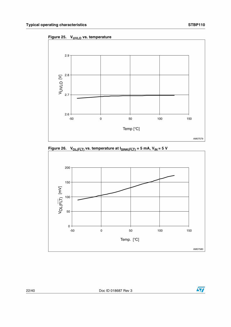
Figure 25. VUVLO vs. temperature
Figure 26. VOL(FLT) vs. temperature at ISINK(FLT) = 5 mA, VIN = 5 V

STBP110 Typical operating characteristics
Doc ID 018687 Rev 3 23/40
Figure 27. RDS(on) vs. temperature at 5 V, 1 A
Figure 28. VIL(EN) vs. temperature

Typical operating characteristics STBP110
24/40 Doc ID 018687 Rev 3
Figure 29. VIH(EN) vs. temperature
Figure 30. I(EN) vs. VIN at V(EN) = 5 V

STBP110 Typical operating characteristics
Doc ID 018687 Rev 3 25/40
Figure 31. RPD(EN) vs. temperature at V(EN) = VIN = 5 V
Figure 32. ton vs. temperature

Typical operating characteristics STBP110
26/40 Doc ID 018687 Rev 3
Figure 33. trec vs. temperature

STBP110 Maximum rating
Doc ID 018687 Rev 3 27/40
6 Maximum rating
Stressing the device above the rating listed in Table 2 may cause permanent damage to the device. These are stress ratings only and operation of the device at these or any other conditions above those indicated in Section 3 of this specification is not implied. Exposure to absolute maximum rating conditions for extended periods may affect device reliability. Refer also to the STMicroelectronics™ SURE Program and other relevant documentation.
Table 2. Absolute maximum ratings
Symbol Parameter Value Unit
TSTG Storage temperature (VIN off) -55 to 150 °C
TSLD(1)
1. Reflow at peak temperature of 260 °C. The time above 255 °C must not exceed 30 seconds.
Lead solder temperature for 10 seconds 260 °C
TJ Operating junction temperature range (internally limited to Toff) -40 to 150 °C
VIN IN pin input voltage -0.3 to 30 V
VOUT OUT pin input/output voltage -0.3 to 12 V
VIO Input/output voltage (other pins) -0.3 to 7 V
ILOAD Load current (IN to OUT) 1200 mA
IREVERSE Reverse diode current (OUT to IN) 500 mA
ISINK(FLT) FLT pin sink current 15 mA
VESD
ESD withstand voltage (IEC 61000-4-2, IN pin only)(2)
2. System-level value (see typical application circuit, C1 ≥ 1 µF low ESR ceramic capacitor).
±15 (air), ±8 (contact)
kV
Human body model (HBM), model = 2(3)
3. Human body model, 100 pF discharged through a 1.5 kΩ resistor according to the JESD22/A114 specification.
2000 V
Machine model (MM), model = B(4)
4. Machine model, 200 pF discharged through all pins according to the JESD22/A115 specification.
200 V
Table 3. Thermal data
Symbol Parameter Value Unit
RthJA Thermal resistance (junction-to-ambient) 59(1)
1. The package was mounted on a 4-layer JEDEC test board with 2 thermal vias connecting from the thermal land to the first buried plane. The 4-layer PCB (2S2P) was constructed based on JESD 51-7 specifications and vias based on JESD 51-5.
°C/W
RthJC Thermal resistance (junction-to-case) 5.9 °C/W

DC and AC parameters STBP110
28/40 Doc ID 018687 Rev 3
7 DC and AC parameters
This section summarizes the operating measurement conditions, and the DC and AC characteristics of the device. The parameters in Table 5 are derived from tests performed under the measurement conditions summarized in Table 4. Designers should check that the operating conditions in their circuit match the operating conditions when relying on the quoted parameters.
Table 4. Operating and AC measurement conditions
Parameter Value Unit
Input voltage (VIN) 5 V
Ambient operating temperature (TA) -40 to 85 °C
Junction operating temperature (TJ) -40 to 125 °C
Logical input rise and fall times 5 ns
Table 5. DC and AC characteristics
Symbol Description Test condition(1) Min. Typ. Max. Unit
VIN Input voltage range VUVLO 28 V
VUVLOInput undervoltage lockout threshold (VIN rising)
Option TOption UOption V
2.52.83.1
2.73.0
3.25
2.93.23.4
V
VHYS(UVLO)Undervoltage lockout hysteresis(2) 100 mV
VOVLO Overvoltage lockout threshold
VIN raises OVLO threshold, option A 5.25 5.375 5.50
V
VIN raises OVLO threshold, option B 5.30 5.50 5.70
VIN raises OVLO threshold, option C 5.71 5.90 6.10
VIN raises OVLO threshold, option D 5.70 6.02 6.40
VIN raises OVLO threshold, option E 6.20 6.40 6.60
VIN raises OVLO threshold, option F 6.60 6.80 7.00
VIN raises OVLO threshold, option G 7.00 7.20 7.40
VHYS(OVLO) Input overvoltage hysteresis 30 60 90 mV
RDS(on) IN to OUT resistance V(EN) = 0 V, VIN = 5 V, ILOAD = 0.5 A 170 280 mΩ
ICC Operating current V(EN)= 0 V, ILOAD = 0 A 140 210µA
ICC(STDBY) Standby current V(EN) = 5 V, ILOAD = 0 A 80 120
VOL(FLT) FLT output low level voltage VIN > VOVLO, ISINK(FLT) = 5 mA 350 800 mV
IL(FLT) FLT output leakage current VFLT = 5 V 0.1 2 µA
VIL(EN) EN low level input voltage 0.4 V

STBP110 DC and AC parameters
Doc ID 018687 Rev 3 29/40
VIH(EN) EN high level input voltage 1.2 V
RPD(EN)EN internal pull-down resistor(3) VIN > 2.5 V, V(EN) = 5 V 100 250 400 kΩ
Timing parameters
ton Startup delay(4) Time measured from VIN > VUVLO to VOUT = 0.3 V (no load on the output).
8 ms
toff(5) Output turn-off time
Time measured from VIN > VOVLO to VOUT ≤ 0.3 V. VIN increasing from 5.0 V to 8.0 V at 3.0 V/µs, RLOAD = 5 Ω, CLOAD = 0.
1
µs
tdis(5) Disable time
Time measured from V(EN) ≥ 1.2 V to VOUT < 0.3 V, RLOAD = 5 Ω, CLOAD = 0.
1 5
trecRecovery delay from UVLO, OVLO, or thermal shutdown(4)
Time measured to VOUT = 0.3 V (no load on the output)
8 ms
Thermal shutdown
ToffThermal shutdown threshold temperature
140 150 °C
THYS(off) Thermal shutdown hysteresis 20 °C
1. Test conditions described in Table 4 (except where noted).
2. Hysteresis of 60 mV typ. available upon request.
3. Version without pull-down resistor or with permanently connected pull-down resistor available upon request.
4. Delays of 16, 32, and 64 ms available upon request.
5. Guaranteed by design. Not tested in production.
Table 5. DC and AC characteristics (continued)
Symbol Description Test condition(1) Min. Typ. Max. Unit

Application information STBP110
30/40 Doc ID 018687 Rev 3
8 Application information
8.1 Calculating the power dissipationThe worst case power dissipation of the STBP110 internal power MOSFET can be calculated using the following formula:
Equation 1
PD = ILOAD2 x RDS(on)(max),
where ILOAD is the load current and RDS(on)(max) is the maximum value of MOSFET resistance.
Example 1
VIN = 5 V, RLOAD = 5 Ω, RDS(on)(max) = 280 mΩ
ILOAD = VIN / (RDS(on)(max) + RLOAD) = 5 / (5 + 0.280) = 0.95 A
PD = 0.952 x 0.28 = 0.25 W
The power dissipation of the reverse diode in powering accessories mode can be estimated as PD = (VOUT - VIN) x IREVERSE ≈ 0.7 x IREVERSE.
8.2 Calculating the junction temperatureThe maximum junction temperature for given power dissipation, ambient temperature, and thermal resistance junction-to-ambient can be calculated as:
Equation 2
TJ = TA + 1.15 x PD x RthJA = TA + 1.15 x ILOAD2 x RDS(on)(max) x RthJA,
where TJ is junction temperature, TA is given ambient temperature, 1.15 is a derating factor, and RthJA is a junction-to-ambient thermal resistance, depending on PCB design. The junction temperature may not exceed 125 °C (see Table 4) to stay within the specified range.
Maximum allowed MOSFET current for ambient temperature TA = 85 °C and various RthJA values are listed in Figure 9.
Example 2
For conditions listed in the previous example, with a well designed PCB (ensuring RthJA = 59 °C/W) and TA = 85 °C, the maximum junction temperature is:
Equation 3
TJ = 85 + 1.15 x 0.25 x 59 = 102 °C,
which is a safe value (below 125 °C).

STBP110 Application information
Doc ID 018687 Rev 3 31/40
8.3 PCB layout recommendations● Input capacitor C1 should be located as close as possible to the STBP110 device. It
should be a low-ESR ceramic capacitor. Also the protective resistors RFLT and REN (if used) should be located close to the STBP110 (see Figure 4).
● For good thermal performance, it is preferred to couple the STBP110 exposed thermal pads with the PCB ground plane. In most designs, this requires thermal vias between the copper pads on the PCB and the ground plane.

Package mechanical data STBP110
32/40 Doc ID 018687 Rev 3
9 Package mechanical data
In order to meet environmental requirements, ST offers these devices in different grades of ECOPACK® packages, depending on their level of environmental compliance. ECOPACK specifications, grade definitions and product status are available at: www.st.com. ECOPACK is an ST trademark.
Figure 34. Package mechanical drawing for TDFN 8-lead (2 x 2 x 0.75 mm)

STBP110 Package mechanical data
Doc ID 018687 Rev 3 33/40
Table 6. Package mechanical dimensions for TDFN 8-lead (2 x 2 x 0.75 mm)(1)
1. Controlling dimension: millimeters.
Symbol
Dimensions
mm inches
Typ. Min. Max. Typ. Min. Max.
A 0.75 0.70 0.80 0.030 0.028 0.031
A1 0.02 0.00 0.05 0.001 0.000 0.002
A3
REF0.20 — — 0.008 — —
b 0.25 0.20 0.30 0.010 0.008 0.012
D
BSC2.00 — — 0.079 — —
D2 1.60 1.45 1.70 0.063 0.057 1.067
E
BSC2.00 — — 0.079 — —
E2 0.90 0.75 1.00 0.035 0.030 0.039
e 0.50 — — 0.020 — —
L 0.30 0.25 0.35 0.012 0.010 0.014
ddd(2)
2. Lead coplanarity should not exceed 0.08 mm.
— — 0.08 — — 0.003
N(3)
3. N is the total number of terminals.
8 8
Tape and reel information STBP110
34/40 Doc ID 018687 Rev 3
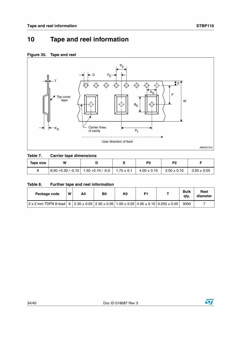
10 Tape and reel information
Figure 35. Tape and reel
Table 7. Carrier tape dimensions
Tape size W D E P0 P2 F
8 8.00 +0.30 / -0.10 1.50 +0.10 / -0.0 1.75 ± 0.1 4.00 ± 0.10 2.00 ± 0.10 3.50 ± 0.05
Table 8. Further tape and reel information
Package code W A0 B0 K0 P1 TBulk qty.
Reel diameter
2 x 2 mm TDFN 8-lead 8 2.30 ± 0.05 2.30 ± 0.05 1.00 ± 0.05 4.00 ± 0.10 0.250 ± 0.05 3000 7

STBP110 Tape and reel information
Doc ID 018687 Rev 3 35/40
Figure 36. Reel dimensions
Figure 37. Tape trailer/leader
Table 9. Reel dimensions
Tape size A max. B min. C D min. N min. G T max.
8 mm 180 (7 inch) 1.5 13 ± 0.2 20.2 60 8.4 +2 / -0 14.4

Tape and reel information STBP110
36/40 Doc ID 018687 Rev 3
Figure 38. Pin 1 orientation
1. Drawings are not to scale.
2. All dimensions are in mm, unless otherwise noted.

STBP110 Part numbering
Doc ID 018687 Rev 3 37/40
11 Part numbering
Note: Currently available part numbers are marked bold in Table 11. For other options, or for more information on any aspect of this device, please contact the nearest ST sales office.
Table 10. Ordering information scheme
STBP110 A T DJ 6 F
Device type
STBP110
Overvoltage threshold
A = 5.375 V
B = 5.50 V
C = 5.90 V
D = 6.02 V
E = 6.40 V
F = 6.80 V
G = 7.20 V
Undervoltage threshold
T = 2.70 V
U = 3.00 V
V = 3.25 V
Package
DJ = TDFN8 2 x 2 x 0.75 mm
Temperature range
6 = -40 °C to +85 °C
Shipping method
F = ECOPACK® package, tape and reel

Package marking information STBP110
38/40 Doc ID 018687 Rev 3
12 Package marking information
Note: Currently available part numbers are marked bold in Table 11. For other options, or for more information on any aspect of this device, please contact the nearest ST sales office.
Table 11. Marking description
Part number Overvoltage threshold (V) Undervoltage threshold (V) Topside marking
STBP110ATxxxx 5.375 2.70 11A
STBP110BTxxxx 5.50 2.70 11B
STBP110CTxxxx 5.90 2.70 11C
STBP110DTxxxx 6.02 2.70 11D
STBP110ETxxxx 6.40 2.70 11E
STBP110FTxxxx 6.80 2.70 11F
STBP110GTxxxx 7.20 2.70 11H
STBP110AUxxxx 5.375 3.00 11K
STBP110BUxxxx 5.50 3.00 11L
STBP110CUxxxx 5.90 3.00 11M
STBP110DUxxxx 6.02 3.00 11N
STBP110EUxxxx 6.40 3.00 11P
STBP110FUxxxx 6.80 3.00 11Q
STBP110GUxxxx 7.20 3.00 11R
STBP110AVxxxx 5.375 3.25 11T
STBP110BVxxxx 5.50 3.25 11U
STBP110CVxxxx 5.90 3.25 11V
STBP110DVxxxx 6.02 3.25 11W
STBP110EVxxxx 6.40 3.25 11X
STBP110FVxxxx 6.80 3.25 11Y
STBP110GVxxxx 7.20 3.25 11Z

STBP110 Revision history
Doc ID 018687 Rev 3 39/40
13 Revision history
Table 12. Document revision history
Date Revision Changes
27-Apr-2011 1 Initial release.
04-May-2011 2 Updated Figure 38.
07-Jun-2012 3
Removed “Preliminary data”, updated Section 2.2, Section 2.4, Section 3.2, Section 3.5, Section 8.2, Figure 3, Figure 9, Figure 38, Table 5, Table 10, Table 11 and Disclaimer, added Section : Typical operating characteristics (STBP110GT), minor text corrections throughout document.
STBP110
40/40 Doc ID 018687 Rev 3
Please Read Carefully:
Information in this document is provided solely in connection with ST products. STMicroelectronics NV and its subsidiaries (“ST”) reserve theright to make changes, corrections, modifications or improvements, to this document, and the products and services described herein at anytime, without notice.
All ST products are sold pursuant to ST’s terms and conditions of sale.
Purchasers are solely responsible for the choice, selection and use of the ST products and services described herein, and ST assumes noliability whatsoever relating to the choice, selection or use of the ST products and services described herein.
No license, express or implied, by estoppel or otherwise, to any intellectual property rights is granted under this document. If any part of thisdocument refers to any third party products or services it shall not be deemed a license grant by ST for the use of such third party productsor services, or any intellectual property contained therein or considered as a warranty covering the use in any manner whatsoever of suchthird party products or services or any intellectual property contained therein.
UNLESS OTHERWISE SET FORTH IN ST’S TERMS AND CONDITIONS OF SALE ST DISCLAIMS ANY EXPRESS OR IMPLIEDWARRANTY WITH RESPECT TO THE USE AND/OR SALE OF ST PRODUCTS INCLUDING WITHOUT LIMITATION IMPLIEDWARRANTIES OF MERCHANTABILITY, FITNESS FOR A PARTICULAR PURPOSE (AND THEIR EQUIVALENTS UNDER THE LAWSOF ANY JURISDICTION), OR INFRINGEMENT OF ANY PATENT, COPYRIGHT OR OTHER INTELLECTUAL PROPERTY RIGHT.
UNLESS EXPRESSLY APPROVED IN WRITING BY TWO AUTHORIZED ST REPRESENTATIVES, ST PRODUCTS ARE NOTRECOMMENDED, AUTHORIZED OR WARRANTED FOR USE IN MILITARY, AIR CRAFT, SPACE, LIFE SAVING, OR LIFE SUSTAININGAPPLICATIONS, NOR IN PRODUCTS OR SYSTEMS WHERE FAILURE OR MALFUNCTION MAY RESULT IN PERSONAL INJURY,DEATH, OR SEVERE PROPERTY OR ENVIRONMENTAL DAMAGE. ST PRODUCTS WHICH ARE NOT SPECIFIED AS "AUTOMOTIVEGRADE" MAY ONLY BE USED IN AUTOMOTIVE APPLICATIONS AT USER’S OWN RISK.
Resale of ST products with provisions different from the statements and/or technical features set forth in this document shall immediately voidany warranty granted by ST for the ST product or service described herein and shall not create or extend in any manner whatsoever, anyliability of ST.
ST and the ST logo are trademarks or registered trademarks of ST in various countries.
Information in this document supersedes and replaces all information previously supplied.
The ST logo is a registered trademark of STMicroelectronics. All other names are the property of their respective owners.
© 2012 STMicroelectronics - All rights reserved
STMicroelectronics group of companies
Australia - Belgium - Brazil - Canada - China - Czech Republic - Finland - France - Germany - Hong Kong - India - Israel - Italy - Japan - Malaysia - Malta - Morocco - Philippines - Singapore - Spain - Sweden - Switzerland - United Kingdom - United States of America
www.st.com