Embed Size (px)
Citation preview
Owen Long, UCSBVERTEX ‘98 Santorini, Greece
The BaBar Silicon Vertex Tracker
Owen LongUniversity of California, Santa Barbara
for the
BaBar Collaboration

Owen Long, UCSBVERTEX ‘98 Santorini, Greece
PEP-II and the BaBar ExperimentPhysics Objective:• CP violation in B meson decays.• Overdetermine the parameters of the CKM quark mixing matrix.
Physics Objective:• CP violation in B meson decays.• Overdetermine the parameters of the CKM quark mixing matrix.
Experimental Approach:• High-luminosity e+e- collider with Upsilon(4s) center-of-mass energy.
• B and anti-B mesons produced coherently.• CP asymmetries depend on t between B decays.• Time-integrated CP asymmetries vanish.• Measurement of B decay points is essential.
• Asymmetric beam energies boost Upsilon(4s) in lab (=0.56).
e- beamdirectionzUpsilon(4s)
decay point B0 decaypoint
B0 decaypoint

Owen Long, UCSBVERTEX ‘98 Santorini, Greece
SVT Institutions
USA:• Lawrence Berkeley National Laboratory
• Stanford University
• University of California, Santa Barbara
• University of California, Santa Cruz
• University of California, San Diego
• University of WisconsinItaly:•Ferrara•Milan•Pavia•Pisa•Torino•Trieste

Owen Long, UCSBVERTEX ‘98 Santorini, Greece
SVT Design Requirements and Constraints
Performance Requirements• z resolution < 130 m.
• Single vertex resolution < 80 m.
• Stand-alone tracking for Pt < 100 MeV/c.
Performance Requirements• z resolution < 130 m.
• Single vertex resolution < 80 m.
• Stand-alone tracking for Pt < 100 MeV/c.
PEP-II Constraints• Permanent dipole (B1) magnets at +/- 20 cm from IP.
• Polar angle restriction: 17.20 < < 1500.• Must be clam-shelled into place after installation of B1 magnets
• Bunch crossing period: 4.2 ns (nearly continuous interactions).
• Radiation exposure at innermost layer (nominal background level):• Average: 33 kRad/year.• In beam plane: 240 kRad/year.
• SVT is designed to function in up to 10 X nominal background.

Owen Long, UCSBVERTEX ‘98 Santorini, Greece
The BaBar Silicon Vertex Tracker
• 5 Layers of double-sided, AC-coupled Silicon.• Custom rad-hard readout IC (the AToM chip).• Low-mass design. ( Pt < 2.7 GeV/c2 for B daughters)• Stand-alone tracking for slow particles.
• Inner 3 layers for angle and impact parameter measurement.• Outer 2 layers for pattern recognition and low Pt tracking.
40 cm30 cm
20 cm

Owen Long, UCSBVERTEX ‘98 Santorini, Greece
Space Frame and Support Cones

Owen Long, UCSBVERTEX ‘98 Santorini, Greece
SVT Geometry
(Arched wedge wafers not shown)
Be Beam pipe1.0 % X0
10 cm
Layer Radius 1 3.3 cm 2 4.0 cm 3 5.9 cm 4 9.1 to 12.7 cm 5 11.4 to 14.6 cm
Layer Radius 1 3.3 cm 2 4.0 cm 3 5.9 cm 4 9.1 to 12.7 cm 5 11.4 to 14.6 cm

Owen Long, UCSBVERTEX ‘98 Santorini, Greece
SVT Modules
Z-SideZ-Side
Phi-SidePhi-Side
Si Wafers Carbon/Kevlar fiberSupport ribs
High DensityInterconnect
(mechanical model) Micro-bondsMicro-bondsFlexible Upilex Fanout
Fanout Properties:• < 0.03 % X0
• 0.52 pF/cm
Fanout Properties:• < 0.03 % X0
• 0.52 pF/cm

Owen Long, UCSBVERTEX ‘98 Santorini, Greece
Ringframe Fixtures Ringframes protect Si wafers and High Density Interconnects (HDIs) during testing.
• “Parking lot” on Fanout enables wafer tests without bonding.
• Bonds for strips with faults plucked before bonding to HDI.
• “Parking lot” on Fanout enables wafer tests without bonding.
• Bonds for strips with faults plucked before bonding to HDI.
• Fanout is cut, glued, and bonded to HDI after wafer testing.
• 1/2 modules are tested again before module assembly.
• Fanout is cut, glued, and bonded to HDI after wafer testing.
• 1/2 modules are tested again before module assembly.

Owen Long, UCSBVERTEX ‘98 Santorini, Greece
SVT High Density Interconnect
AToMChips
UpilexFanout
MountingButtons
BergConnector
Flexible Tail (testing version)Functions:
• Mounting and cooling for readout ICs.
• Mechanical mounting point for module.
Functions:
• Mounting and cooling for readout ICs.
• Mechanical mounting point for module.
Features:• AlN substrate.• Double sided.• Thermistor for temp. monitor.• 3 different models.
Features:• AlN substrate.• Double sided.• Thermistor for temp. monitor.• 3 different models.

Owen Long, UCSBVERTEX ‘98 Santorini, Greece
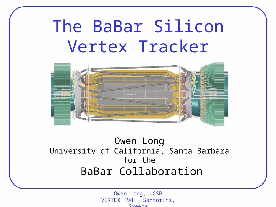
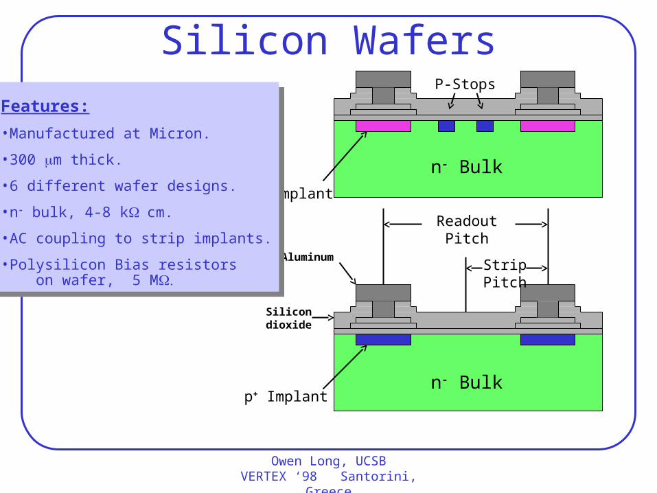
Silicon Wafers
Features:
•Manufactured at Micron.
•300 m thick.
•6 different wafer designs.
•n- bulk, 4-8 kcm.
•AC coupling to strip implants.
•Polysilicon Bias resistors on wafer, 5 M
Features:
•Manufactured at Micron.
•300 m thick.
•6 different wafer designs.
•n- bulk, 4-8 kcm.
•AC coupling to strip implants.
•Polysilicon Bias resistors on wafer, 5 M
Owen Long, UCSBVERTEX ‘98 Santorini, Greece
Silicon Wafers
Bias ring p+ Implant
Al
p+ strip side
P-stop n+ Implant
Polysiliconbias resistor
Polysiliconbias resistor
Edge guard ring
Edge guard ring
n+ strip side
50 m
55 m

Owen Long, UCSBVERTEX ‘98 Santorini, Greece
Measured Wafer Characteristics Strip Properties
n-side n-side n-side p-side
•Strip Pitch: 50 m55 m 105 m 50 m
•Inter-strip C: 1.1 pF/cm 1.0 pF/cm 1.0 pF/cm 1.1 pF/cm
•AC decoupling C: 20 pF/cm 22 pF/cm 34 pF/cm 43 pF/cm
•Implant-to-back C: 0.19 pF/cm 0.36 pF/cm 0.17 pF/cm
•Bias R: 4 to 8 M 4 to 8 M 4 to 8 M 4 to 8 M
Strip Propertiesn-side n-side n-side p-side
•Strip Pitch: 50 m55 m 105 m 50 m
•Inter-strip C: 1.1 pF/cm 1.0 pF/cm 1.0 pF/cm 1.1 pF/cm
•AC decoupling C: 20 pF/cm 22 pF/cm 34 pF/cm 43 pF/cm
•Implant-to-back C: 0.19 pF/cm 0.36 pF/cm 0.17 pF/cm
•Bias R: 4 to 8 M 4 to 8 M 4 to 8 M 4 to 8 M
Bulk Properties•Bias current: 0.1 to 1.0 A
•Bulk current: 0.1 to 1.0 A
•Depletion voltage: 35 to 45 V
Bulk Properties•Bias current: 0.1 to 1.0 A
•Bulk current: 0.1 to 1.0 A
•Depletion voltage: 35 to 45 V

Owen Long, UCSBVERTEX ‘98 Santorini, Greece
Detector-Fanout AssembliesStatus:• All wafers are glued to fanouts, bonded, and tested.• Over 0.3 million bonds.
Status:• All wafers are glued to fanouts, bonded, and tested.• Over 0.3 million bonds.
Fault Types:• Pinhole - Break in the AC coupling capacitor, short between metal and implant.• P-stop short (DC) - Bond foot breaks through oxide layer shorting metal and p-stop.• High current (DC) - Low value for bias resistor.• Unbondable - Damaged or obstructed bond pad, rework not possible.
Fault Types:• Pinhole - Break in the AC coupling capacitor, short between metal and implant.• P-stop short (DC) - Bond foot breaks through oxide layer shorting metal and p-stop.• High current (DC) - Low value for bias resistor.• Unbondable - Damaged or obstructed bond pad, rework not possible.
Fault ChannelsPinhole 1 - 2 %DC-fault 1 - 2 %Other 1 %
Total faults: 2 - 4 %
Fault ChannelsPinhole 1 - 2 %DC-fault 1 - 2 %Other 1 %
Total faults: 2 - 4 %

Owen Long, UCSBVERTEX ‘98 Santorini, Greece
The AToM Chip
Features:•128 Channels per chip•Rad-Hard CMOS process (Honeywell)•Simultaneous
– Acquisition– Digitization– Readout
•Sparsified readout•Time Over Threshold (TOT) readout•Internal charge injection
Features:•128 Channels per chip•Rad-Hard CMOS process (Honeywell)•Simultaneous
– Acquisition– Digitization– Readout
•Sparsified readout•Time Over Threshold (TOT) readout•Internal charge injection
AToM = A Time Over threshold MachineAToM = A Time Over threshold Machine
Custom Si readout IC designed for BaBar by:• LBNL• INFN-Pavia• UCSC
Custom Si readout IC designed for BaBar by:• LBNL• INFN-Pavia• UCSC
5.7 mm
8.3 m
m

Owen Long, UCSBVERTEX ‘98 Santorini, Greece
The AToM Chip
CAL DAC
Shaper
ThreshDAC
CompPREAMP
TOT CounterTime Stamp
Event TimeEvent Number
Revolving Buffer
193 Bins
Si
Buffer
Buffer
Chan # Sp
ars
ifica
tion
Re
ad
ou
t Bu
ffer
CINJ
CAC
SerialData Out
Amp, Shape, Discr, Calib•5-bit CAL DAC (0.5 fC/count)•5-bit Thr DAC (0.05 fC/count)•Shaping time 100 - 400 ns
Amp, Shape, Discr, Calib•5-bit CAL DAC (0.5 fC/count)•5-bit Thr DAC (0.05 fC/count)•Shaping time 100 - 400 ns
Trigger Latency Buffer•15 MHz Sample rate•Total storage = 12.7 us
Trigger Latency Buffer•15 MHz Sample rate•Total storage = 12.7 us
TOT, Tstamp, Buffering•4 bits TOT (logarithmic)•5 bits Hit Tstamp
(67 ns/count)•4 buffers / channel
TOT, Tstamp, Buffering•4 bits TOT (logarithmic)•5 bits Hit Tstamp
(67 ns/count)•4 buffers / channel
15 MHz

Owen Long, UCSBVERTEX ‘98 Santorini, Greece
Threshold ScanProcedure
• Fix charge injection value• Scan Threshold DAC (0-63)
1 Threshold DAC count = 10.5 mV10.5 mV/count / Gain = 0.053 fC / count
• Fit Hit efficiency vs Threshold to Error FunctionWidth = Noise50% point = Offset for Qinj
Procedure• Fix charge injection value• Scan Threshold DAC (0-63)
1 Threshold DAC count = 10.5 mV10.5 mV/count / Gain = 0.053 fC / count
• Fit Hit efficiency vs Threshold to Error FunctionWidth = Noise50% point = Offset for Qinj
Gain Measurement• 3 threshold scans at different Qinj values• Fit 50% point vs Qinj
• Slope is Gain (thr/Q in mV/fC)• Intercept is Threshold DAC offset
Gain Measurement• 3 threshold scans at different Qinj values• Fit 50% point vs Qinj
• Slope is Gain (thr/Q in mV/fC)• Intercept is Threshold DAC offset
Threshold
Hits
Offset
Noise
Qinj Counts
Offs
et C
ount
s
Threshold DACOffset

Owen Long, UCSBVERTEX ‘98 Santorini, Greece
TOT and Charge Scan
CAL DAC CAL DAC
Injected Charge (fC) Injected Charge (fC)
Tim
e O
ver
Thr
esho
ld
Tim
e O
ver
Thr
esho
ld
1 MIP 1 MIP
• Scan calibration DAC (0-63) at a fixed threshold.
• Range of injected charge: 0 to 30 fC (1 MIP = 3.8 fC)
• Measure Time Over Threshold (TOT) response.
• Hit TOT stored in 4 bits (1-15).
• Scan calibration DAC (0-63) at a fixed threshold.
• Range of injected charge: 0 to 30 fC (1 MIP = 3.8 fC)
• Measure Time Over Threshold (TOT) response.
• Hit TOT stored in 4 bits (1-15).
Owen Long, UCSBVERTEX ‘98 Santorini, Greece
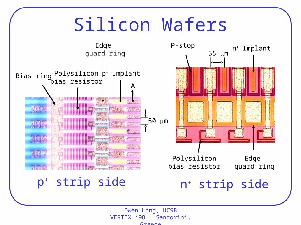
Measured Noise and Gain
Chip PropertiesThreshold offset dispersion: 14 mV or 440 eleChip power consumption:0.57 W/chip, 4.5 mW/chan
Chip PropertiesThreshold offset dispersion: 14 mV or 440 eleChip power consumption:0.57 W/chip, 4.5 mW/chan
100 ns 200 ns 400 ns
AToM-I, test board: 450 ele + 47 ele/pF 375 ele + 45 ele/pF 325 ele + 39 ele/pFAToM-II, test board: 350 ele + 40 ele/pF 275 ele + 35 ele/pF 225 ele + 26 ele/pF
AToM-I, Layer 2 mod: Phi-side 1350 ele 1200 ele 1050 ele Z-side 1050 ele 850 ele 750 ele
AToM-I, Gain: 190 mV/fC 235 mV/fC 200 mV/fCAToM-II, Gain: 300 mV/fC
• Total strip capacitance ranges from 11 to 37 pF.• Threshold setting of 4 X Noise still well below 1 MIP ( about 20,000 ele ).
AToM-II measurementsare preliminary.

Owen Long, UCSBVERTEX ‘98 Santorini, Greece
AToM IC and Wafer Characteristics After Exposure to Radiation
AToM-I ChipAfter exposure to 2.4 MRad with Co60 source
• Gain dropped 0 to 20 %
Power off during exposure Power on during exposure C=0 dNoise/dC C=0 dNoise/dC
Noise Increase 15 to 80 % 15 to 50 % 5 to 10 % < 5%
• Only 3 chips tested. Will check this result with more tests.
AToM-I ChipAfter exposure to 2.4 MRad with Co60 source
• Gain dropped 0 to 20 %
Power off during exposure Power on during exposure C=0 dNoise/dC C=0 dNoise/dC
Noise Increase 15 to 80 % 15 to 50 % 5 to 10 % < 5%
• Only 3 chips tested. Will check this result with more tests.
Silicon WafersAfter exposure to 1 MRad of photons from a Co60 source
• <17% increase in interstrip capacitance
• Current density <350 nA/cm2, mostly generation at Si - insulator surface
Silicon WafersAfter exposure to 1 MRad of photons from a Co60 source
• <17% increase in interstrip capacitance
• Current density <350 nA/cm2, mostly generation at Si - insulator surface

Owen Long, UCSBVERTEX ‘98 Santorini, Greece
Production and Construction• Silicon Wafers:
• All wafers in hand.• Wafers glued to fanouts, bonded, and tested.
• Front-End Electronics:• High Density Interconnect (HDI) substrate production nearly complete.• 2 lots of AToM-I in hand. AToM-II testing underway.• Several HDIs loaded, tested, and bonded to detectors.
• Mechanical:• Support cones, space frame, and mounting rings complete.• Ready to begin module assembly.
• Back-End Electronics:• Production complete. Loading and testing.
• Estimated date of completion: Early March 1999.
• Silicon Wafers: • All wafers in hand.• Wafers glued to fanouts, bonded, and tested.
• Front-End Electronics:• High Density Interconnect (HDI) substrate production nearly complete.• 2 lots of AToM-I in hand. AToM-II testing underway.• Several HDIs loaded, tested, and bonded to detectors.
• Mechanical:• Support cones, space frame, and mounting rings complete.• Ready to begin module assembly.
• Back-End Electronics:• Production complete. Loading and testing.
• Estimated date of completion: Early March 1999.

Owen Long, UCSBVERTEX ‘98 Santorini, Greece
PEP-II at SLACThe PEPII Collider at SLAC• Luminosity: 3 x 1033 to 1034 cm-2 s-1
• 30 to 100 million Upsilon(4s) per year.
• Beams collided head-on (no crossing angle).
• Bunch crossing period: 4.2 ns• Interactions effectively continuous.• Permanent dipole magnets required close to interaction point.
The PEPII Collider at SLAC• Luminosity: 3 x 1033 to 1034 cm-2 s-1
• 30 to 100 million Upsilon(4s) per year.
• Beams collided head-on (no crossing angle).
• Bunch crossing period: 4.2 ns• Interactions effectively continuous.• Permanent dipole magnets required close to interaction point.

Owen Long, UCSBVERTEX ‘98 Santorini, Greece
SVT Mechanical FeaturesCarbon fiber
Space Frame
Carbon fiber support cones
Brasscooling rings
B1 dipolepermanent magnet
(inside support cone)
B1 dipolepermanent magnet
(inside support cone)
109 cm
22 cm

Owen Long, UCSBVERTEX ‘98 Santorini, Greece
SVT Mechanical Features
Silicon wafers
Carbon & Kevlar fiber support ribs

Owen Long, UCSBVERTEX ‘98 Santorini, Greece
SVT ModulesLayer Number of
WafersTotal Phi-Strip LengthBackward Forward
Z-Strip Length
5b 8 26.5 cm 26.5 cm 4.1 to 5.1 cm
5a 8 26.5 cm 25.1 cm 4.2 to 5.1 cm
4b 7 22.4 cm 19.9 cm 4.2 to 5.1 cm
3 6 12.8 cm 12.8 cm 7.0 cm
2 4 8.8 cm 8.8 cm 4.8 cm1 4 8.2 cm 8.2 cm 4.0 cm
4a 7 22.4 cm 18.5 cm 4.2 to 5.1 cm
Owen Long, UCSBVERTEX ‘98 Santorini, Greece
Silicon WafersP-Stops
n- Bulk
n- Bulk
n+ Implant
p+ Implant
StripPitch
Silicondioxide
Aluminum
Features:
•Manufactured at Micron.
•300 m thick.
•6 different wafer designs.
•n- bulk, 4-8 kcm.
•AC coupling to strip implants.
•Polysilicon Bias resistors on wafer, 5 M
Features:
•Manufactured at Micron.
•300 m thick.
•6 different wafer designs.
•n- bulk, 4-8 kcm.
•AC coupling to strip implants.
•Polysilicon Bias resistors on wafer, 5 M
ReadoutPitch

Owen Long, UCSBVERTEX ‘98 Santorini, Greece
Wafer Specifications
Used in Layers1,2, and 3
Used in Layers4 and 5
Owen Long, UCSBVERTEX ‘98 Santorini, Greece
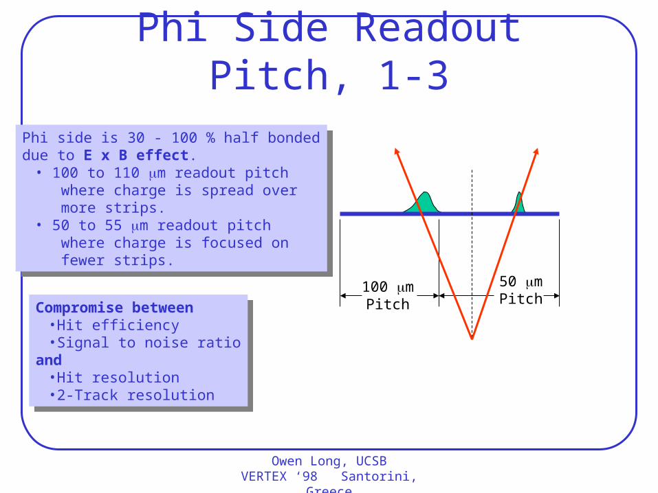
Phi Side Readout Pitch, 1-3
100 mPitch
50 mPitch
Phi side is 30 - 100 % half bondeddue to E x B effect.
• 100 to 110 m readout pitch where charge is spread over more strips.• 50 to 55 m readout pitch where charge is focused on fewer strips.
Phi side is 30 - 100 % half bondeddue to E x B effect.
• 100 to 110 m readout pitch where charge is spread over more strips.• 50 to 55 m readout pitch where charge is focused on fewer strips.
Compromise between • Hit efficiency• Signal to noise ratio
and• Hit resolution• 2-Track resolution
Compromise between • Hit efficiency• Signal to noise ratio
and• Hit resolution• 2-Track resolution
Owen Long, UCSBVERTEX ‘98 Santorini, Greece
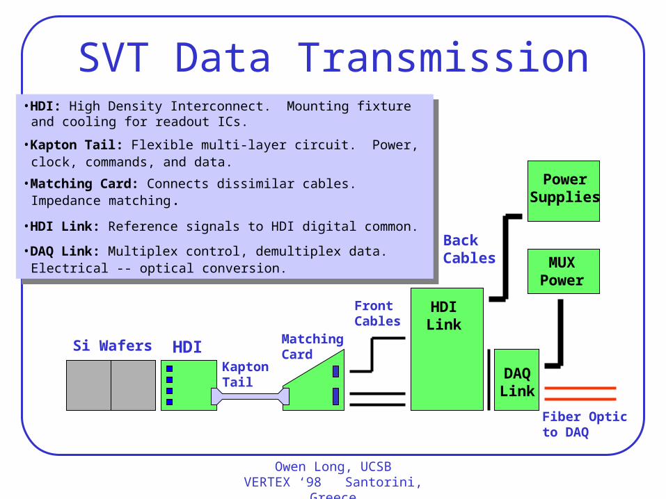
SVT Data Transmission
HDI MatchingCard
KaptonTail
FrontCables
Si Wafers
HDILink
DAQLink
PowerSupplies
MUXPower
BackCables
Fiber Opticto DAQ
•HDI: High Density Interconnect. Mounting fixture and cooling for readout ICs.
•Kapton Tail: Flexible multi-layer circuit. Power, clock, commands, and data.
•Matching Card: Connects dissimilar cables. Impedance matching.
•HDI Link: Reference signals to HDI digital common.
•DAQ Link: Multiplex control, demultiplex data. Electrical -- optical conversion.

Owen Long, UCSBVERTEX ‘98 Santorini, Greece
CalibrationInternal charge injection used for
• Measuring Gain, Noise, and Threshold Offsets• Identifying shorts and bad channels• Examining Time Over Threshold (TOT) response• Testing digital functionality
Internal charge injection used for• Measuring Gain, Noise, and Threshold Offsets• Identifying shorts and bad channels• Examining Time Over Threshold (TOT) response• Testing digital functionality
Charge injection circuit• 5-bit DAC (0-63)• 1 DAC count = 0.48 fC• Range 0 - 30 fC (1 MIP = 4 fC)
Charge injection circuit• 5-bit DAC (0-63)• 1 DAC count = 0.48 fC• Range 0 - 30 fC (1 MIP = 4 fC)
Calibration methods• Threshold scan (Gain, Noise, Offsets)• Charge scan (TOT response)
Calibration methods• Threshold scan (Gain, Noise, Offsets)• Charge scan (TOT response)