Embed Size (px)
Citation preview
Owen SullivanG. W. Woodruff School
of Mechanical Engineering,
Georgia Institute of Technology,
771 First Drive,
Atlanta, GA 30332
e-mail: [email protected]
Man Prakash GuptaG. W. Woodruff School
of Mechanical Engineering,
Georgia Institute of Technology,
771 First Drive,
Atlanta, GA 30332
e-mail: [email protected]
Saibal MukhopadhyayDepartment of Electrical
and Computer Engineering,
Georgia Institute of Technology,
266 Ferst Drive,
Atlanta, GA 30332
e-mail: [email protected]
Satish KumarG. W. Woodruff School
of Mechanical Engineering,
Georgia Institute of Technology,
771 First Drive,
Atlanta, GA 30332
e-mail: [email protected]
On-Chip Power GenerationUsing Ultrathin ThermoelectricGeneratorsThermoelectric generators (TEGs) can significantly improve the net power consumptionand battery life of the low power mobile devices or high performance devices by generat-ing power from their waste heat. Recent advancements also show that the ultrathin ther-moelectric devices can be fabricated and integrated within a micro-electronic package.This work investigates the power generation by an ultrathin TEG embedded within amicro-electronic package considering several key parameters such as load resistance,chip heat flux, and proximity of the TEG to chip. The analysis shows that the power gener-ation from TEGs increases with increasing background heat flux on chip or when TEGsare moved closer to the chip. An array of embedded TEGs is considered in order to ana-lyze the influence of multiple TEGs on total power generation and conversion efficiency.Increasing the number of TEGs from one to nine increases the useful power generationfrom 72.9 mW to 378.4 mW but decreases the average conversion efficiency from 0.47% to0.32%. The average power generated per TEG gradually decrease from 72.9 mW to 42.0mW when number of TEGs is increased from one to nine, but the total useful power gener-ated using nine TEGs is significant and emphasize the benefits of using embedded TEGs toreduce net power consumption in electronics packages. [DOI: 10.1115/1.4027995]
Keywords: thermoelectric generators, harvesting, waste heat, embedded, Seebeckcoefficient
1 Introduction
TEGs produce an electromotive effect, known as the Seebeckvoltage, when a temperature difference is applied across the twoends of the device. TEGs have been used on spacecraft to providean energy source millions of miles away from the Earth’s surface[1]. This is an extreme case where other energy sources may notbe available. TEGs have also been widely used to generate powerfor remote data communication system used in oil and gas pipe-lines and for polar weather stations [2]. Some studies have alsodelved into the possible use of TEGs in automobile exhaust pipesto reduce the load on a vehicle’s alternator [3]. Recently, the pos-sibility of humans wearing TEGs to power various biomedicalsensors has been explored [4]. There are many possible applica-tions of TEGs but improving the efficiency of TEGs is still thebiggest challenge which is required to be overcome to make thesedevices cost-effective and attractive solution as a green and com-mercially viable technology. Suitable materials which can provideoptimized properties (i.e., very low thermal conductivity, veryhigh electrical conductivity, and high Seebeck coefficient) forhigh figure of merit are being explored with some promising can-didates already discovered but more work is still required [5]. Oneof the interesting applications is to embed TEGs inside anelectronic package for energy harvesting from chip waste heat.Embedded TEGs can reduce the net power consumption of a chip,but this important application of TEGs is relatively less exploredand focus of the present study.
Besides the material properties, temperature difference acrossthe TEG also determines its efficiency. Different TEG materials
obtain their optimum efficiency in different temperature regimes,and therefore different applications may require different TEGmaterials depending upon the available temperature difference.Crane et al. built a generator consisting of many smaller TEGs anddemonstrated 130 W of power generation from a 205 �C tempera-ture difference [6]. This is a significantly large power output by aTEG, but such large temperature difference is not available in mostscenarios. Small temperature differences are available across manyelectronic devices, which can be used to harvest energy by TEGs toenhance the overall energy efficiency of the system. Solbrekkenet al. attached 1 mm thick TEGs to a portable device’s central proc-essing unit (CPU) and powered a fan using available temperaturedifference of approximately 30 �C to generate 40–50 mW of power[7]. The fan was able to keep the CPU temperature below 85 �C ina 35 �C ambient environment [7]. This hybrid cooling solution har-vests energy from the waste heat and power a fan to remove heatfrom the package, turning an active form of cooling into a passiveform since it no longer requires a battery to power fan [7]. Thepower generated by TEGs can also be used to assist the powersource of micropumps for microchannel cooling of electronic pack-ages [8–10]. If the TEGs can be moved closer to heat dissipatingelements, higher power can be harvested, e.g., embedding TEGinside the package. However, the integration of TEGs inside thepackage can be challenging for high performance computing ormobile technologies. Particularly, 1 mm thick TEGs are too thick tobe embedded inside electronic packages. Bi2Te3 superlattice basedthermoelectric cooler (TEC) has been fabricated and integratedwithin an electronic package by Chowdhury et al. [11]; this TE de-vice is thin enough (�100 lm) to be embedded within a typicalmicro-electronic package [11].
Bi and Te based TE materials have high figure of merit at roomtemperature and so they are one of the best TE materials for hotspot cooling inside or energy harvesting from a micro-electronic
Contributed by the Electronic and Photonic Packaging Division of ASME forpublication in the JOURNAL OF ELECTRONIC PACKAGING. Manuscript received February3, 2014; final manuscript received June 13, 2014; published online October 6, 2014.Assoc. Editor: Gongnan Xie.
Journal of Electronic Packaging MARCH 2015, Vol. 137 / 011005-1Copyright VC 2015 by ASME
Downloaded From: http://electronicpackaging.asmedigitalcollection.asme.org/ on 10/06/2014 Terms of Use: http://asme.org/terms
package [12,13]. The Bi2Te3 superlattice based ultrathin TECsshowed increased performance compared to the TECs made byother materials [11]. Bi2Te3 based TE devices can be fabricatedusing standard semiconductor manufacturing techniques, whichallows these devices to be relatively easily integrated within apackage [14]. Use of standard semiconductor manufacturing toolsallows scaling of the devices to cater to the power generation needof a particular device, e.g., from simple modules providing a fewmilliwatts to interconnected module-arrays providing tens of watts[13]. Some recent research has investigated the possibility ofusing silicon nanowires as potential TE material [15]. Silicon ispoor thermoelectric material in its bulk form, but the figure ofmerit of rough silicon nanowires (�1) can be two orders of magni-tude higher than bulk Si (�0.01) [15]. Li et al. fabricated siliconnanowire based TEGs, which has footprint of 5 mm� 5 mm con-sisting 162 thermocouples, and generated 1.5 nW with a 0.12 Ktemperature difference [15]. Silicon nanowires based TEGs areCMOS compatible compared to the Bi, Te, Sb, and Se basedTEGs and thus could be integrated much closer to the electroniccircuitry [15]. However, the power generation by silicon nanowirebased embedded TEGs is still very low and significant work isrequired to improve its efficiency. Bi2Te3 based TEG seems morepromising and hence chosen for investigation by the present work.
Some studies focused on power generation using TEGsattached to a micro-electronic package [6,7,16–19], but the inves-tigation of power generation using Bi2Te3 based ultrathin TEGsembedded within an electronic packaging has not been addressed.Gould et al. integrated a TEG on a desktop computer’s CPU andattached a heat sink to the other side of the TEG [20]. This TE de-vice generated power in the range of hundreds of microwatts tofew milliwatts [20]. The temperature difference across the deviceis very low (�2 �C) as it was integrated outside the electronicpackage [20]. Embedding a TEG inside an electronic package,closer to the heat source can provide larger temperature differen-ces across its TE element. Most of the previous models of theTEGs consider constant temperatures at the hot and cold junctions[6,16–19]. Constant temperatures at the two junctions of theTEGs is applicable in only few situations, e.g., fluid flow on bothsides of a TEG with different temperatures [18]. For embeddedTEGs, the package environment can significantly affect the powergeneration and efficiency of TEGs. So, it is crucial to consider theeffect of the structure and properties of packaging materials andthe boundary conditions. Several recent works have suggestedthat maximum power generation in complex systems correspondsto the case when the load resistance is greater than the device re-sistance rather than when they are equal [7,21]. This deviationfrom the expected behavior occurs if the temperatures of the junc-tions are not kept constant, and such a situation is more realisticand applicable for a larger set of scenarios including embeddedTEGs. It is important to analyze the optimum load resistance forpower generation by TEGs embedded inside a package that has noconstant temperature boundaries. This is addressed in the presentstudy.
In our previous work [22,23], we have developed numericalmodel of a package with embedded TECs. The dimensions andproperties of these devices are similar to the devices fabricated byChowdhury et al. [11]. The present work builds on these previousmodels to explore the possibility of using packaged thin-filmsuperlattice based TE devices as TEGs. The goal of the presentwork is to investigate the power generation by Bi2Te3 superlatticebased TEGs embedded inside an electronic package. This workfirst outlines the development of the 3D numerical model of thepackage and multiple embedded TEGs for a steady-state opera-tion. Section 4 presents an analysis of one TEG located at the cen-ter of the package and decipher the effect of key parameters: loadresistance, background heat flux, and proximity of TEG to chip onpower generation. Then, multiple TEGs are added to the packageand comparison of various configurations of TEGs is performed toexplore the power generation capability and efficiency of arrayof embedded TEGs. Finally, transient operation of the TEG is
investigated to understand the response of TEGs subjected to achange in the background heat flux.
2 Computational Methodology
This section outlines the computational methodology used indeveloping model for the package and embedded TEGs. Themodel for TEGs embedded within an electronic package is devel-oped using the commercial computational fluid dynamics (CFD)package FLUENT and meshing software GAMBIT. The model solvesFourier’s conduction equations for the electronic package and theTEG modules and provides temperature distributions for the entiresystem. The TEG modules are attached at the back side of theheat spreader. Each module has 49 p–n couple and has an area of3 mm� 3 mm. The TE material is Bi2Te3 based superlattice whichis 8 lm thick sandwiched between two 46 lm thick copper layers,resulting in a total TEG thickness of 100 lm. The computationaldomain of the model includes the heat spreader, thermal interfacematerial, chip, and TEGs. The properties of the TE and thermalinterface material are obtained from the Ref. [11] and its supple-mentary material. The heat sink is modeled as a convectiveboundary condition at the top surface of the heat spreader with aconvection coefficient, h, of 2050 W/m2-K. This value of convec-tion coefficient is estimated from the previous computation byGupta et al. [22] in order to match the numerical results of thepackaged TEC with the experimental and numerical results pre-sented in Ref. [11]. The detailed information about the heat sinkgeometry in Ref. [11] is not provided, but using the available in-formation, the effective convection coefficient was estimated andresults were within 1–2 �C of those presented in Ref. [11].
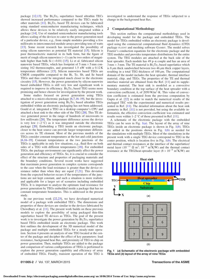
A schematic of the electronic package with the embeddedTEGs can be seen in Fig. 1(a). The layout of the array of nineTEGs inside an electronic package is shown in Fig. 1(b). TEGsare added in the positions shown in Fig. 1(b) as needed forthe simulations with multiple TEGs. Most of the simulations in thepresent work with a single TEG device correspond to TEG in thecenter position, which is location five in Fig. 1(b). The electricaland thermal contact resistances at the interface of the superlattice/metal layer (10�11 X m2; 10�6 m2K/W) and the thermal contactresistance at the TEG/heat-spreader layer (8� 10�6 m2K/W) are
Fig. 1 (a) Schematic of the electronic package with embeddedTEGs and (b) layout of the array of nine TEGs
011005-2 / Vol. 137, MARCH 2015 Transactions of the ASME
Downloaded From: http://electronicpackaging.asmedigitalcollection.asme.org/ on 10/06/2014 Terms of Use: http://asme.org/terms
taken from Ref. [11]. The geometry, thermoelectric properties, andcontact resistances of packaged TEGs considered in the presentwork is similar to those of the TECs used in Refs. [22] and [23]and are also provided in Table 1. The cooling performance of theseTECs has been validated against experimental results in our previ-ous work [22].
3 Governing Equations
The governing differential equations for the thermal transportinside the electronic package is represented as
@2T
@x2þ @
2T
@y2þ @
2T
@z2þ _Q ¼ @T
a@t(1.1)
where
_Q ¼I2
A2rkinside TEC
0 elsewhere
8<:
9=; (1.2)
Here, T is temperature, a is thermal diffusivity, I is current, A isthe area of an element, r is electrical conductivity, and k is ther-mal conductivity.
A heat flux boundary condition is applied at the bottom of thechip, which can be expressed as
� k@T
@y¼ q00 (1.3)
where q00 ¼ 42.7 W/cm2 unless otherwise specified.In addition, at the hot end of the TEG,
�kA@T
@y
����y¼yþ
h
¼ �kA@T
@yþ SIT
� �y¼y�
h
þ I2Relec (1.4)
Here, the y coordinate is directed from TEG to the heat spreader,and yþh and y�h are locations just above and below the hot junction,respectively. S is the Seebeck coefficient and Relec is the contactelectrical resistance of the TEG. Also, at the cold end of the TEG
�kA@T
@y
����y¼yþc
¼ �kA@T
@y� SIT
� �y¼y�c
þ I2Relec (1.5)
where yþc and y�c are locations just above and below the cold junc-tion, respectively.
Finally, at the top surface of the heat spreader,
� k@T
@y¼ hðT � T1Þ (1.6)
where h is the convective heat transfer coefficient and T1 is theambient air temperature, which is taken to be 300 K for allsimulations.
In addition to the material properties and boundary conditionsof the package, thermoelectric power generation depends on theseveral factors: Seebeck coefficient, temperature differencebetween the hot and cold junctions of the TEG, and the resistancesof the TEG and load. The equation for Seebeck voltage of TEGdevice can be given as
V ¼ SðTH � TCÞ (1.7)
where S is the Seebeck coefficient, TH is the temperature of thehot junction, and TC is the temperature of the cold junction. It issimple to determine the current through TEG once Seebeck volt-age is estimated using the expression
I ¼ V
R¼ SðTH � TCÞ
RL þ RTEG
(1.8)
Here, RL is the electrical resistance of load and RTEG is the totalelectrical resistance of the TEG device (including contact resistan-ces). The amount of useful work, WU, is the power dissipatedthrough the load resistance and can be evaluated by
WU ¼ I2RL ¼SðTH � TCÞRL þ RTEG
� �2
RL (1.9)
A current flows through the thermoelectric device when it isconnected to external load which in turn reduce the temperatureof the hot junction due to Peltier effects. Therefore, the Peltiereffect must also be taken into account. Peltier cooling of the TEGdevice is incorporated by adding heat (aSITc) at the cold junctionand subtracting heat (aSITh) from the hot junction of the TEG,where Th and Tc are the temperatures of the hot and cold junctions,respectively. The value of S is considered to be 300 lV/K whichis based on the experimental measurements in Ref. [11]. The heatgeneration due to the electrical resistance of the TEG device andthe electrical resistances at contact is considered by adding an I2Rterm at the corresponding volumes and layers. The thermal con-tact resistances were considered by adding appropriate thermalresistances at the interfaces.
The simulations are performed using the finite volume methodbased commercial solver FLUENT. 200 K cells are considered forthe simulations; grid independence tests verify that these cells aresufficient for further simulations.
4 Power Generation Using Single TEG
This section studies the power generated by a single3 mm� 3 mm TEG located at position five in Fig. 1(b) as a func-tion of the load resistance. The current flow, voltage, and tempera-ture across the TEG is investigated to understand the response ofTEG embedded inside a micro-electronic package for a uniformbackground heat flux of 100 W/cm2 at the bottom of chip.
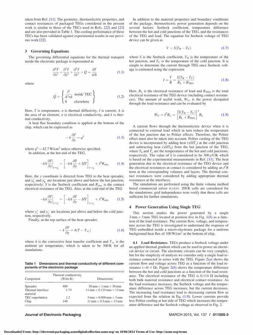
4.1 Load Resistance. TEGs produce a Seebeck voltage underan applied thermal gradient which can be used to power an electri-cal device or circuit. The electronic circuits can be very complex,but for the simplicity of analysis we consider only a single load re-sistance connected in series with the TEG. Figure 2(a) shows thecurrent flow and voltage across TEG as a function of the load re-sistance (�0–1 X). Figure 2(b) shows the temperature differencebetween the hot and cold junctions as a function of the load resist-ance. The electrical resistance of the TEG is 0.114 X includingboth bulk material resistance and electrical contact resistance. Asthe load resistance increases, the Seebeck voltage and the temper-ature difference across TEG increases, but the current decreases.The increasing load resistance lead to decreasing current flow asexpected from the relation in Eq. (1.9). Lower currents provideless Peltier cooling at hot side of TEG which increases the temper-ature difference and the Seebeck voltage as observed in Fig. 2.
Table 1 Dimensions and thermal conductivity of different com-ponents of the electronic package
ComponentThermal conductivity
(W/m-K) Dimensions
Spreader 400 30 mm� 1 mm� 30 mmThermal interfacematerial
1.75 11 mm� 0.125 mm� 13 mm
TEC-superlattice 1.2 3 mm� 0.008 mm� 3 mmChip 140 11 mm� 0.5 mm� 13 mm
Journal of Electronic Packaging MARCH 2015, Vol. 137 / 011005-3
Downloaded From: http://electronicpackaging.asmedigitalcollection.asme.org/ on 10/06/2014 Terms of Use: http://asme.org/terms
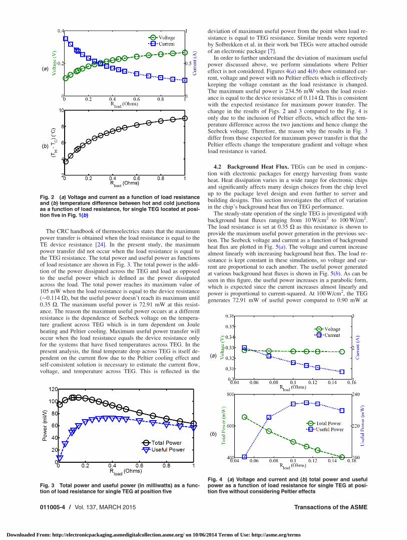
The CRC handbook of thermoelectrics states that the maximumpower transfer is obtained when the load resistance is equal to theTE device resistance [24]. In the present study, the maximumpower transfer did not occur when the load resistance is equal tothe TEG resistance. The total power and useful power as functionsof load resistance are shown in Fig. 3. The total power is the addi-tion of the power dissipated across the TEG and load as opposedto the useful power which is defined as the power dissipatedacross the load. The total power reaches its maximum value of105 mW when the load resistance is equal to the device resistance(�0.114 X), but the useful power doesn’t reach its maximum until0.35 X. The maximum useful power is 72.91 mW at this resist-ance. The reason the maximum useful power occurs at a differentresistance is the dependence of Seebeck voltage on the tempera-ture gradient across TEG which is in turn dependent on Jouleheating and Peltier cooling. Maximum useful power transfer willoccur when the load resistance equals the device resistance onlyfor the systems that have fixed temperatures across TEG. In thepresent analysis, the final temperate drop across TEG is itself de-pendent on the current flow due to the Peltier cooling effect andself-consistent solution is necessary to estimate the current flow,voltage, and temperature across TEG. This is reflected in the
deviation of maximum useful power from the point when load re-sistance is equal to TEG resistance. Similar trends were reportedby Solbrekken et al. in their work but TEGs were attached outsideof an electronic package [7].
In order to further understand the deviation of maximum usefulpower discussed above, we perform simulations where Peltiereffect is not considered. Figures 4(a) and 4(b) show estimated cur-rent, voltage and power with no Peltier effects which is effectivelykeeping the voltage constant as the load resistance is changed.The maximum useful power is 234.56 mW when the load resist-ance is equal to the device resistance of 0.114 X. This is consistentwith the expected resistance for maximum power transfer. Thechange in the results of Figs. 2 and 3 compared to the Fig. 4 isonly due to the inclusion of Peltier effects, which affect the tem-perature difference across the two junctions and hence change theSeebeck voltage. Therefore, the reason why the results in Fig. 3differ from those expected for maximum power transfer is that thePeltier effects change the temperature gradient and voltage whenload resistance is varied.
4.2 Background Heat Flux. TEGs can be used in conjunc-tion with electronic packages for energy harvesting from wasteheat. Heat dissipation varies in a wide range for electronic chipsand significantly affects many design choices from the chip levelup to the package level design and even further to server andbuilding designs. This section investigates the effect of variationin the chip’s background heat flux on TEG performance.
The steady-state operation of the single TEG is investigated withbackground heat fluxes ranging from 10 W/cm2 to 100 W/cm2.The load resistance is set at 0.35 X as this resistance is shown toprovide the maximum useful power generation in the previous sec-tion. The Seebeck voltage and current as a function of backgroundheat flux are plotted in Fig. 5(a). The voltage and current increasealmost linearly with increasing background heat flux. The load re-sistance is kept constant in these simulations, so voltage and cur-rent are proportional to each another. The useful power generatedat various background heat fluxes is shown in Fig. 5(b). As can beseen in this figure, the useful power increases in a parabolic form,which is expected since the current increases almost linearly andpower is proportional to current-squared. At 100 W/cm2, the TEGgenerates 72.91 mW of useful power compared to 0.90 mW at
Fig. 2 (a) Voltage and current as a function of load resistanceand (b) temperature difference between hot and cold junctionsas a function of load resistance, for single TEG located at posi-tion five in Fig. 1(b)
Fig. 3 Total power and useful power (in milliwatts) as a func-tion of load resistance for single TEG at position five
Fig. 4 (a) Voltage and current and (b) total power and usefulpower as a function of load resistance for single TEG at posi-tion five without considering Peltier effects
011005-4 / Vol. 137, MARCH 2015 Transactions of the ASME
Downloaded From: http://electronicpackaging.asmedigitalcollection.asme.org/ on 10/06/2014 Terms of Use: http://asme.org/terms
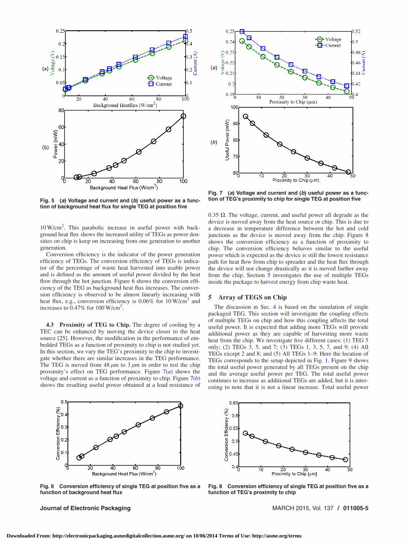
10 W/cm2. This parabolic increase in useful power with back-ground heat flux shows the increased utility of TEGs as power den-sities on chip is keep on increasing from one generation to anothergeneration.
Conversion efficiency is the indicator of the power generationefficiency of TEGs. The conversion efficiency of TEGs is indica-tor of the percentage of waste heat harvested into usable powerand is defined as the amount of useful power divided by the heatflow through the hot junction. Figure 6 shows the conversion effi-ciency of the TEG as background heat flux increases. The conver-sion efficiency is observed to be almost linearly increasing withheat flux, e.g., conversion efficiency is 0.06% for 10 W/cm2 andincreases to 0.47% for 100 W/cm2.
4.3 Proximity of TEG to Chip. The degree of cooling by aTEC can be enhanced by moving the device closer to the heatsource [25]. However, the modification in the performance of em-bedded TEGs as a function of proximity to chip is not studied yet.In this section, we vary the TEG’s proximity to the chip to investi-gate whether there are similar increases in the TEG performance.The TEG is moved from 48 lm to 3 lm in order to test the chipproximity’s effect on TEG performance. Figure 7(a) shows thevoltage and current as a function of proximity to chip. Figure 7(b)shows the resulting useful power obtained at a load resistance of
0.35 X. The voltage, current, and useful power all degrade as thedevice is moved away from the heat source or chip. This is due toa decrease in temperature difference between the hot and coldjunctions as the device is moved away from the chip. Figure 8shows the conversion efficiency as a function of proximity tochip. The conversion efficiency behaves similar to the usefulpower which is expected as the device is still the lowest resistancepath for heat flow from chip to spreader and the heat flux throughthe device will not change drastically as it is moved further awayfrom the chip. Section 5 investigates the use of multiple TEGsinside the package to harvest energy from chip waste heat.
5 Array of TEGS on Chip
The discussion in Sec. 4 is based on the simulation of singlepackaged TEG. This section will investigate the coupling effectsof multiple TEGs on chip and how this coupling affects the totaluseful power. It is expected that adding more TEGs will provideadditional power as they are capable of harvesting more wasteheat from the chip. We investigate five different cases: (1) TEG 5only; (2) TEGs 3, 5, and 7; (3) TEGs 1, 3, 5, 7, and 9; (4) AllTEGs except 2 and 8; and (5) All TEGs 1–9. Here the location ofTEGs corresponds to the setup depicted in Fig. 1. Figure 9 showsthe total useful power generated by all TEGs present on the chipand the average useful power per TEG. The total useful powercontinues to increase as additional TEGs are added, but it is inter-esting to note that it is not a linear increase. Total useful power
Fig. 5 (a) Voltage and current and (b) useful power as a func-tion of background heat flux for single TEG at position five
Fig. 6 Conversion efficiency of single TEG at position five as afunction of background heat flux
Fig. 7 (a) Voltage and current and (b) useful power as a func-tion of TEG’s proximity to chip for single TEG at position five
Fig. 8 Conversion efficiency of single TEG at position five as afunction of TEG’s proximity to chip
Journal of Electronic Packaging MARCH 2015, Vol. 137 / 011005-5
Downloaded From: http://electronicpackaging.asmedigitalcollection.asme.org/ on 10/06/2014 Terms of Use: http://asme.org/terms
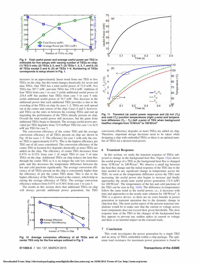
increases in an approximately linear trend from one TEG to fiveTEGs on the chip, but this trend changes drastically for seven andnine TEGs. One TEG has a total useful power of 72.9 mW, fiveTEGs has 307.7 mW, and nine TEGs has 378.4 mW. Addition offour TEGs from case 1 to case 3 yields additional useful power of234.8 mW but another four TEGs from case 3 to case 5 onlyyields additional useful power of 70.7 mW. This decrease in theadditional power that each additional TEG provides is due to thecrowding of the TEGs on chip. In cases 1–3, TEGs are well spreadout at the center and corners of the chip. Cases 4 and 5, however,add TEGs on the sides in between the existing TEGs and end updegrading the performance of the TEGs already present on chip.Overall the total useful power still increases, but the gains fromadditional TEGs begin to diminish. The average useful power pro-vided per TEG degrades from 72.9 mWper TEG for case 1 to 42.0mW per TEG for case 5.
The conversion efficiency of the center TEG and the averageconversion efficiency of all TEGs present on chip are shown inFig. 10 for cases 1–5. The efficiency for case 1 with only the cen-ter TEG is approximately 0.47%. This is the highest efficiency perTEG out of all cases considered. The conversion efficiency of thecenter TEG at location five degrades drastically as more TEGs areadded on the chip. The efficiency of center TEG decreases from0.47% to 0.32% from case 1 of single TEG to case 5 of nineTEGs on the chip. Additional TEGs on chip reduces the heat fluxthrough the center TEG as it is no longer the sole low resistancepath, and this decreases the temperature difference between thehot and cold junctions significantly. The average conversion effi-ciency of all TEGs present on the chip is consistently higher thanthe efficiency of just the center TEG alone. This is due to thehigher efficiency of the TEGs located at the corners, which help inraising the average efficiency of TEGs. The average conversionefficiency reduces from 0.47% to 0.36% from case 1 to case 5.
The results in this section show that additional TEGs on chipwill always provide additional power generation, but TEG
conversion efficiency degrades as more TEGs are added on chip.Therefore, important design decisions need to be taken whiledesigning a chip with embedded TEGs as there is an optimal num-ber of TEGs for a desired total power.
6 Transient Response
In this section, we study the transient response of TEGs sub-jected to change in the background heat flux. Figure 11(a) showsthe useful power of a TEG as the background heat flux is changedfrom 10 W/cm2 to 100 W/cm2. We observe a small lag betweenthe heat flux change and the initial response of the TEG due to thetime needed in any significant change in temperature across theTEG. As soon as the temperature difference across the TEG startincreasing, the useful power also begins to increase and finallyapproaches the steady-state useful power generation (72.9 mW)for 100 W/cm2. The temperatures of the hot and cold junctions ofthe TEG can be seen in Fig. 11(b). The difference in temperaturesfollow the same trend as the useful power, i.e., it increases withtime and approaches to the steady-state solution for 100 W/cm2. ATEG is a passive device, so there are no extra benefits in powergeneration in transient operation due to the dynamic change inchip heat flux. The most useful aspect of the present transient sim-ulations would be to make sure that the current or voltage acrossload components does not exceed their given thresholds. The slowresponse time of the TEG to the changes of the background heatflux appears to prevent any sudden spikes in current or voltageand there is no harmful impact on the external loads.
7 Conclusion
This work investigates the power generation by a single TEGand an array of TEGs embedded within a chip package. The opti-mum load resistance for maximum power generation is found to
Fig. 9 Total useful power and average useful power per TEG inmilliwatts for five setups with varying number of TEGs on chip:(1) TEG 5 only; (2) TEGs 3, 5, and 7; (3) TEGs 1, 3, 5, 7, and 9; (4)all TEGs except 2 and 8; (5) all TEGs 1–9. Numbering of TEGscorresponds to setup shown in Fig. 1.
Fig. 10 Average conversion efficiency of all TEGs and ofcenter TEG only for the five setups outlined in Fig. 9
Fig. 11 Transient (a) useful power response and (b) hot (TH)and cold (TC) junction temperatures (right y-axis) and tempera-ture difference (TH 2 TC) (left y-axis) of TEG when backgroundheatflux changes from 10 W/cm2 to 100 W/cm2
011005-6 / Vol. 137, MARCH 2015 Transactions of the ASME
Downloaded From: http://electronicpackaging.asmedigitalcollection.asme.org/ on 10/06/2014 Terms of Use: http://asme.org/terms
be 0.35 X, which deviates from the initial expectations of the loadresistance to be equal to the device resistance (0.11 X). This dis-crepancy is found to be due to the TEG’s performance depend-ence on the temperature difference between the hot and coldjunctions, which changes with the current and resulting Peltiereffect. Increasing background heat flux increases temperature dif-ference across the TEG and results in higher power generation.Temperature difference across TEG also increases when it ismoved closer to the chip resulting in increase in useful power gen-eration. The total useful power increases from 72.9 mW to 378.4mW as the number of TEGs in the package is increased from oneto nine. The negative aspect of having more TEGs on chip is theaverage power generated per TEG decreases from 72.9 mW perTEG for a single TEG to 42.0 mW per TEG for nine TEGs. Tran-sient behavior of TEGs in response to increasing heat flux showsno advantage in power generation. The net power generation fromTEGs will continue to improve as better thermoelectric materialswill be discovered. There are interesting design choices to bemade when embedding TEGs in chip. In future work, one of theimportant steps to consider is to address the specifics of how thepower generated by TEGs can be utilized on chip and which por-tions of the chip will benefit most from this technology.
Acknowledgment
The authors acknowledge the support from National ScienceFoundation Grant No. ECCS-1028569.
Nomenclature
I ¼ current (A)RL ¼ load resistance (W)
RTEG ¼ device resistance (W)S ¼ Seebeck coefficient (V/K)t ¼ time (s)
T ¼ temperature (�C)V ¼ voltage (V)
References[1] Bell, L. E., 2008, “Cooling, Heating, Generating Power, and Recovering Waste
Heat With Thermoelectric Systems,” Science, 321(5895), pp. 1457–1461.[2] DiSalvo, F. J., 1999, “Thermoelectric Cooling and Power Generation,” Science,
285(5428), pp. 703–706.[3] Thacher, E. F., Helenbrook, B. T., Karri, M. A., and Richter, C. J., 2007,
“Testing of an Automobile Exhaust Thermoelectric Generator in a LightTruck,” Proc. Inst. Mech. Eng., Part D, 221(D1), pp. 95–107.
[4] Wang, Z. Y., Leonov, V., Fiorini, P., and Van Hoof, C., 2009, “Realization of aWearable Miniaturized Thermoelectric Generator for Human BodyApplications,” Sens. Actuators, A, 156(1), pp. 95–102.
[5] Zhao, L.-D., Lo, S.-H., Zhang, Y., Sun, H., Tan, G., Uher, C., Wolverton, C.,Dravid, V. P., and Kanatzidis, M. G., 2014, “Ultralow Thermal Conductivityand High Thermoelectric Figure of Merit in SnSe Crystals,” Nature, 508(7496),pp. 373–377.
[6] Crane, D. T., LaGrandeur, J. W., Harris, F., and Bell, L. E., 2009, “PerformanceResults of a High-Power-Density Thermoelectric Generator: Beyond theCouple,” J. Electron. Mater., 38(7), pp. 1375–1381.
[7] Solbrekken, G. L., Yazawa, K., and Bar-Cohen, A., 2008, “Heat Driven Cool-ing of Portable Electronics Using Thermoelectric Technology,” IEEE Trans.Adv. Packag., 31(2), pp. 429–437.
[8] Xie, G., Chen, Z., Sunden, B., and Zhang, W., 2012, “Numerical Predictions ofthe Flow and Thermal Performance of Water-Cooled Single-Layer and Double-Layer Wavy Microchannel Heat Sinks,” Numer. Heat Transfer, Part A, 63(3),pp. 201–225.
[9] Xie, G., Liu, J., Zhang, W., and Sunden, B., 2012, “Analysis of Flow andThermal Performance of a Water-Cooled Transversal Wavy MicrochannelHeat Sink for Chip Cooling,” ASME J. Electron. Packag., 134(4),p. 041010.
[10] Xie, G., Liu, J., Liu, Y., Sunden, B., and Zhang, W., 2013, “Comparative Studyof Thermal Performance of Longitudinal and Transversal-Wavy MicrochannelHeat Sinks for Electronic Cooling,” ASME J. Electron. Packag., 135(2),p. 021008.
[11] Chowdhury, I., Prasher, R., Lofgreen, K., Chrysler, G., Narasimhan, S., Maha-jan, R., Koester, D., Alley, R., and Venkatasubramanian, R., 2009, “On-ChipCooling by Superlattice-Based Thin-Film Thermoelectrics,” Nat. Nanotechnol.,4(4), pp. 235–238.
[12] Venkatasubramanian, R., Siivola, E., Colpitts, T., and O’Quinn, B., 2001,“Thin-Film Thermoelectric Devices With High Room-Temperature Figures ofMerit,” Nature, 413(6856), pp. 597–602.
[13] Venkatasubramanian, R., Watkins, C., Stokes, D., Posthill, J., and Caylor, C.,2007, “Energy Harvesting for Electronics With Thermoelectric Devices UsingNanoscale Materials,” IEEE International Electron Devices Meeting (IEDM2007), Washington, DC, December 10–12, pp. 367–370.
[14] Strasser, M., Aigner, R., Lauterbach, C., Sturm, T. F., Franosh, M., andWachutka, G., 2003, “Micromachined CMOS Thermoelectric Generatorsas On-Chip Power Supply,” 12th International Conference on Transducers,Solid-State Sensors, Actuators and Microsystems, Boston, MA, June 8–12,pp. 45–48.
[15] Li, Y., Buddharaju, K., Singh, N., Lo, G. Q., and Lee, S. J., 2011, “Chip-LevelThermoelectric Power Generators Based on High-Density Silicon NanowireArray Prepared With Top-Down CMOS Technology,” IEEE Electron DeviceLett., 32(5), pp. 674–676.
[16] Min, C., Rosendahl, L. A., Condra, T. J., and Pedersen, J. K., 2009, “NumericalModeling of Thermoelectric Generators With Varing Material Properties in aCircuit Simulator,” IEEE Trans. Energy Convers., 24(1), pp. 112–124.
[17] Xiao, H., Gou, X. L., and Yang, C., 2008, “Simulation Analysis on Thermoelec-tric Generator System Performance,” 7th International Conference on SystemSimulation and Scientific Computing (ICSC 2008), Beijing, China, October10–12, pp. 1183–1187.
[18] Chen, M., Rosendahl, L. A., and Condra, T., 2011, “A Three-DimensionalNumerical Model of Thermoelectric Generators in Fluid Power Systems,” Int.J. Heat Mass Transfer, 54(1–3), pp. 345–355.
[19] Crane, D. T., Kossakovski, D., and Bell, L. E., 2009, “Modeling the BuildingBlocks of a 10% Efficient Segmented Thermoelectric Power Generator,”J. Electron. Mater., 38(7), pp. 1382–1386.
[20] Gould, C. A., Shammas, N. Y. A., Grainger, S., and Taylor, I., 2011,“Thermoelectric Cooling of Microelectronic Circuits and Waste Heat ElectricalPower Generation in a Desktop Personal Computer,” Mater. Sci. Eng., B,176(4), pp. 316–325.
[21] Snyder, G. J., and Ursell, T. S., 2003, “Thermoelectric Efficiency andCompatibility,” Phys. Rev. Lett., 91(14), p. 148301.
[22] Gupta, M. P., Sayer, M. H., Mukhopadhyay, S., and Kumar, S., 2011, “UltrathinThermoelectric Devices for On-Chip Peltier Cooling,” IEEE Trans. Compon.,Packag. Manuf. Technol., 1(9), pp. 1395–1405.
[23] Sullivan, O., Gupta, M. P., Mukhopadhyay, S., and Kumar, S., 2012, “Array ofThermoelectric Coolers for On-Chip Thermal Management,” ASME J.Electron. Packag., 134(2), p. 021005.
[24] Rowe, D. M., 1995, CRC Handbook of Thermoelectrics, Taylor & Francis,New York.
[25] Sullivan, O., Alexandrov, B., Mukhopadhyay, S., and Kumar, S., 2012,“Compact Model of Thermoelectric Coolers on a Micro-Electronic Chip,”ASME Paper No. IMECE2011-64881.
Journal of Electronic Packaging MARCH 2015, Vol. 137 / 011005-7
Downloaded From: http://electronicpackaging.asmedigitalcollection.asme.org/ on 10/06/2014 Terms of Use: http://asme.org/terms