Embed Size (px)
Citation preview
Performance Analysis of Novel 600V Super-JunctionPower LDMOS Transistors with Embedded P-Type
Round Pillars
K. Permthammasin*, G. Wachutka*, M. Schmitt** and H. Kapels**
* Institute for Physics of Electrotechnology, Munich University of Technology,80290 Munich, Germany
[email protected], [email protected]
** Infineon Technologies AG, Balanstrasse 59, 81541 Munich, [email protected], [email protected]
Abstract — A novel 600V super-junction (SJ)power LDMOS device with two different designs ofSJ structures has been proposed. The basic SJstructure consists of a number of p-type roundpillars buried in an n-type drift layer down to a p-type substrate. Performance characteristics of thedevice in terms of the trade-off between on-stateresistance and breakdown voltage and the sensitivityof the voltage blocking to charge imbalance in the SJstructure were analyzed by means of 3D numericalsimulation. The studies show that designing the SJstructure such that it counteracts the substrate-aideddepletion effect leads to a significantly reducedsensitivity of the blocking voltage to chargefluctuation at the expense of a slightly degradedperformance trade-off.
I. INTRODUCTION
The recent realization of the super-junction (SJ)concept [1,2] represents a significant breakthrough inovercoming the operation limits of conventional silicon-based high power MOS devices. The SJ concept isbased on the principle of charge compensation inalternatively stacked, heavily doped p- and n-typecolumns, known as SJ structure. In the on-state, theheavily doped n-type columns conduct the forwardcurrent through the drift zone with strongly reduced on-resistance. In the blocking state, already at a relativelysmall reverse-biased voltage all the columns arecompletely depleted of mobile charges. On conditionthat the space charges in the depleted columnscompensate each other, the electric field will be nearlyuniformly distributed over the whole drift region. As a
result, a substantial increase in breakdown voltage canbe achieved.
So far the SJ concept has been commerciallyrealized in vertical double diffused MOS (VDMOS)transistors such as the CoolMOSTM [1] and theMDmeshTM [2]. In lateral double diffused MOS(LDMOS) devices [3,4], however, the presence of the p-type substrate considerably affects the chargecompensation in the SJ structure because, under reversebias, a non-uniform vertical depletion layer forms at thep-substrate/n-drift junction. The normally flat surfaceelectric field becomes distorted by this substrate-aideddepletion effect, with the result that the blockingcapability of the device deteriorates.
This work deals with the 3D numerical analysis of anovel 600V SJ power LDMOS transistor suitable foruse in smart power ICs. Two different SJ structures areconsidered: one is designed to suppress the substrateeffect, whereas the other one serves as reference forcomparison. We performed comparative 3D-simulationsin order to investigate the performance limitations of thetwo designs, together with the sensitivity of theirblocking capability to the unavoidable dopingfluctuations in the SJ structure.
II. DEVICE STRUCTURE
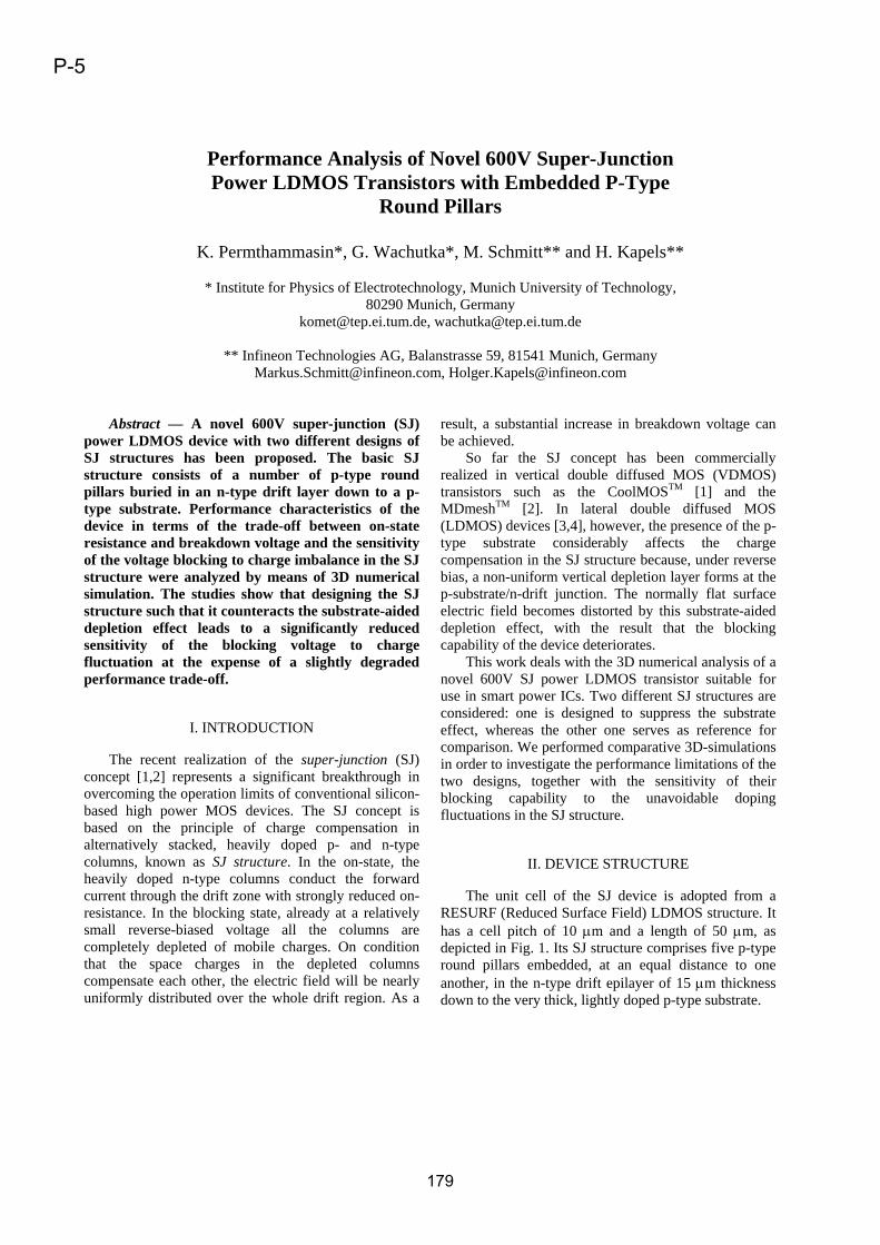
The unit cell of the SJ device is adopted from aRESURF (Reduced Surface Field) LDMOS structure. Ithas a cell pitch of 10 µm and a length of 50 µm, asdepicted in Fig. 1. Its SJ structure comprises five p-typeround pillars embedded, at an equal distance to oneanother, in the n-type drift epilayer of 15 µm thicknessdown to the very thick, lightly doped p-type substrate.
179
P-5
GateSource Drain
P-Substrate
N-Drift Region
pp p p p
Source Gate Drain
P-Substrate
N-Drift Region
pp p p p
Figure 1: Device structure of the SJ LDMOS underinvestigation.
Top: uniform SJ. Bottom: non-uniform SJ.
One design, where all the round pillars have thesame diameter of 6 µm, is referred to as uniform SJ.Although such a uniform structure helps to equallydistribute the surface electric field over the drift region,it is not able to efficiently suppress the substrate-aideddepletion effect. For this purpose, another structuraldesign, denoted as non-uniform SJ, is proposed. Here,the round pillars are arrayed with decreasing size alongthe entire length of the drift region, starting with thethickest one, whose diameter is 7 µm, near the sourceand diminishing in steps of 0.5 µm such that the pillarnearest to the drain is thinnest with a diameter of 5 µm.This non-uniform configuration is supposed tocounterbalance the gradient in space charge in thesubstrate during the blocking state.
III. PERFORMANCE TRADE-OFF
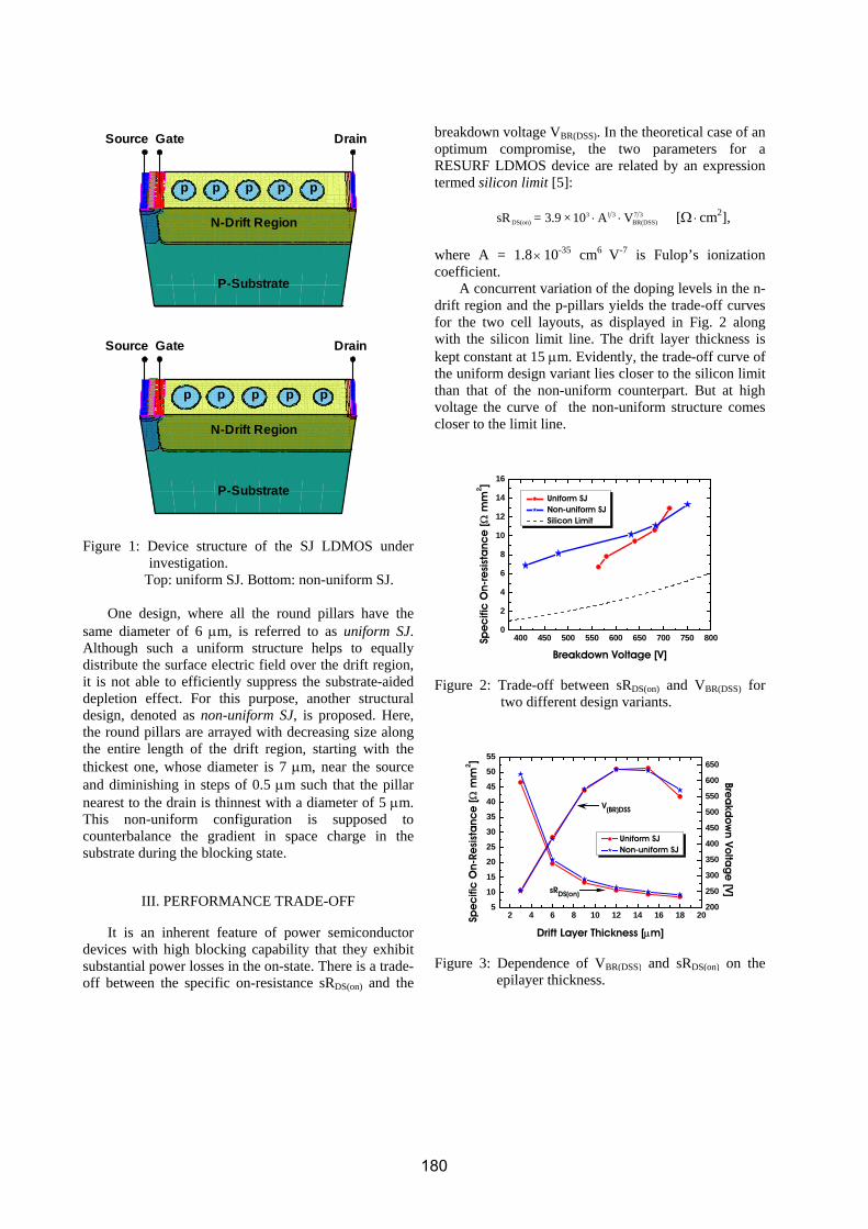
It is an inherent feature of power semiconductordevices with high blocking capability that they exhibitsubstantial power losses in the on-state. There is a trade-off between the specific on-resistance sRDS(on) and the
breakdown voltage VBR(DSS). In the theoretical case of anoptimum compromise, the two parameters for aRESURF LDMOS device are related by an expressiontermed silicon limit [5]:
3 1 3 7 3DS(on) BR(DSS)sR = 3.9 ×10 A V⋅ ⋅ [Ω ⋅ cm2],
where A = 1.8 × 10⁻³⁵ cm6 V-7 is Fulop’s ionizationcoefficient.
A concurrent variation of the doping levels in the n-drift region and the p-pillars yields the trade-off curvesfor the two cell layouts, as displayed in Fig. 2 alongwith the silicon limit line. The drift layer thickness iskept constant at 15 µm. Evidently, the trade-off curve ofthe uniform design variant lies closer to the silicon limitthan that of the non-uniform counterpart. But at highvoltage the curve of the non-uniform structure comescloser to the limit line.
400 450 500 550 600 650 700 750 8000
2
4
6
8
10
12
14
16
Spe
cifi
c O
n-re
sist
anc
e [
Ω m
m2 ]
Breakdown Voltage [V]
Uniform SJ Non-uniform SJ Silicon Limit
Figure 2: Trade-off between sRDS(on) and VBR(DSS) fortwo different design variants.
2 4 6 8 10 12 14 16 18 205
10
15
20
25
30
35
40
45
50
55
Drift Layer Thickness [µm]
Spe
cifi
c O
n-Re
sist
anc
e [Ω
mm
2 ]
sRDS(on)
V(BR)DSS
200
250
300
350
400
450
500
550
600
650
Uniform SJ Non-uniform SJ
Brea
kdo
wn Vo
ltag
e [V]
Figure 3: Dependence of VBR(DSS) and sRDS(on) on theepilayer thickness.
180
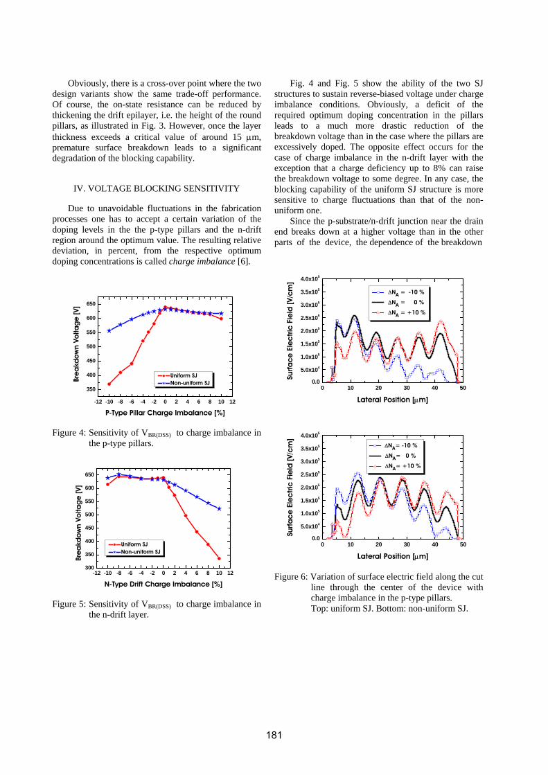
Obviously, there is a cross-over point where the twodesign variants show the same trade-off performance.Of course, the on-state resistance can be reduced bythickening the drift epilayer, i.e. the height of the roundpillars, as illustrated in Fig. 3. However, once the layerthickness exceeds a critical value of around 15 µm,premature surface breakdown leads to a significantdegradation of the blocking capability.
IV. VOLTAGE BLOCKING SENSITIVITY
Due to unavoidable fluctuations in the fabricationprocesses one has to accept a certain variation of thedoping levels in the the p-type pillars and the n-driftregion around the optimum value. The resulting relativedeviation, in percent, from the respective optimumdoping concentrations is called charge imbalance [6].
-12 -10 -8 -6 -4 -2 0 2 4 6 8 10 12
350
400
450
500
550
600
650
Bre
akd
ow
n Vo
ltag
e [V
]
P-Type Pillar Charge Imbalance [%]
Uniform SJ Non-uniform SJ
Figure 4: Sensitivity of VBR(DSS) to charge imbalance inthe p-type pillars.
-12 -10 -8 -6 -4 -2 0 2 4 6 8 10 12300
350
400
450
500
550
600
650
Bre
akd
ow
n Vo
ltag
e [V
]
N-Type Drift Charge Imbalance [%]
Uniform SJ Non-uniform SJ
Figure 5: Sensitivity of VBR(DSS) to charge imbalance inthe n-drift layer.
Fig. 4 and Fig. 5 show the ability of the two SJstructures to sustain reverse-biased voltage under chargeimbalance conditions. Obviously, a deficit of therequired optimum doping concentration in the pillarsleads to a much more drastic reduction of thebreakdown voltage than in the case where the pillars areexcessively doped. The opposite effect occurs for thecase of charge imbalance in the n-drift layer with theexception that a charge deficiency up to 8% can raisethe breakdown voltage to some degree. In any case, theblocking capability of the uniform SJ structure is moresensitive to charge fluctuations than that of the non-uniform one.
Since the p-substrate/n-drift junction near the drainend breaks down at a higher voltage than in the otherparts of the device, the dependence of the breakdown
0 10 20 30 40 500.0
5.0x10⁴
1.0x10⁵
1.5x10⁵
2.0x10⁵
2.5x10⁵
3.0x10⁵
3.5x10⁵
4.0x10⁵
Surfa
ce
Ele
ctr
ic F
ield
[V/c
m]
Lateral Position [µm]
∆NA = -10 %
∆NA = 0 %
∆NA = +10 %
0 10 20 30 40 500.0
5.0x10⁴
1.0x10⁵
1.5x10⁵
2.0x10⁵
2.5x10⁵
3.0x10⁵
3.5x10⁵
4.0x10⁵
Surf
ac
e E
lec
tric
Fie
ld [V
/cm
]
Lateral Position [µm]
∆NA= -10 %
∆NA= 0 %
∆NA= +10 %
Figure 6: Variation of surface electric field along the cutline through the center of the device withcharge imbalance in the p-type pillars.Top: uniform SJ. Bottom: non-uniform SJ.
181
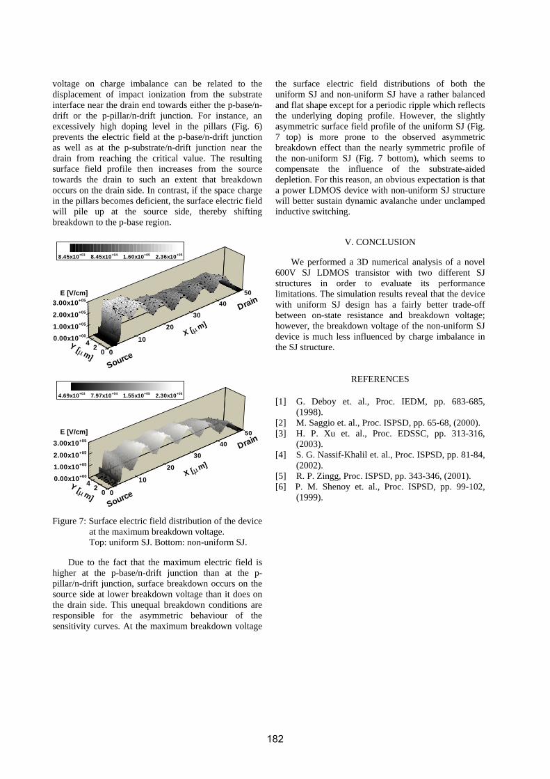
voltage on charge imbalance can be related to thedisplacement of impact ionization from the substrateinterface near the drain end towards either the p-base/n-drift or the p-pillar/n-drift junction. For instance, anexcessively high doping level in the pillars (Fig. 6)prevents the electric field at the p-base/n-drift junctionas well as at the p-substrate/n-drift junction near thedrain from reaching the critical value. The resultingsurface field profile then increases from the sourcetowards the drain to such an extent that breakdownoccurs on the drain side. In contrast, if the space chargein the pillars becomes deficient, the surface electric fieldwill pile up at the source side, thereby shiftingbreakdown to the p-base region.
0.00x10+00
1.00x10+05
2.00x10+05
3.00x10+05
0
10
20
30
40
50
X [ m]
024Y [ m]
8.45x10+03 8.45x10+04 1.60x10+05 2.36x10+05
µ
µ
E [V/cm]
Source
Drain
0.00x10+00
1.00x10+05
2.00x10+05
3.00x10+05
0
10
20
30
40
50
X [ m]
024Y [ m]
4.69x10+03 7.97x10+04 1.55x10+05 2.30x10+05
µ
µ
E [V/cm]
Source
Drain
Figure 7: Surface electric field distribution of the deviceat the maximum breakdown voltage.Top: uniform SJ. Bottom: non-uniform SJ.
Due to the fact that the maximum electric field ishigher at the p-base/n-drift junction than at the p-pillar/n-drift junction, surface breakdown occurs on thesource side at lower breakdown voltage than it does onthe drain side. This unequal breakdown conditions areresponsible for the asymmetric behaviour of thesensitivity curves. At the maximum breakdown voltage
the surface electric field distributions of both theuniform SJ and non-uniform SJ have a rather balancedand flat shape except for a periodic ripple which reflectsthe underlying doping profile. However, the slightlyasymmetric surface field profile of the uniform SJ (Fig.7 top) is more prone to the observed asymmetricbreakdown effect than the nearly symmetric profile ofthe non-uniform SJ (Fig. 7 bottom), which seems tocompensate the influence of the substrate-aideddepletion. For this reason, an obvious expectation is thata power LDMOS device with non-uniform SJ structurewill better sustain dynamic avalanche under unclampedinductive switching.
V. CONCLUSION
We performed a 3D numerical analysis of a novel600V SJ LDMOS transistor with two different SJstructures in order to evaluate its performancelimitations. The simulation results reveal that the devicewith uniform SJ design has a fairly better trade-offbetween on-state resistance and breakdown voltage;however, the breakdown voltage of the non-uniform SJdevice is much less influenced by charge imbalance inthe SJ structure.
REFERENCES
[1] G. Deboy et. al., Proc. IEDM, pp. 683-685,(1998).
[2] M. Saggio et. al., Proc. ISPSD, pp. 65-68, (2000).[3] H. P. Xu et. al., Proc. EDSSC, pp. 313-316,
(2003).[4] S. G. Nassif-Khalil et. al., Proc. ISPSD, pp. 81-84,
(2002).[5] R. P. Zingg, Proc. ISPSD, pp. 343-346, (2001).[6] P. M. Shenoy et. al., Proc. ISPSD, pp. 99-102,
(1999).
182