Embed Size (px)
Citation preview

1 of 24
Optimum Technology Matching® Applied
GaAs HBT
InGaP HBTGaAs MESFET
SiGe BiCMOSSi BiCMOSSiGe HBT
GaAs pHEMTSi CMOSSi BJT
GaN HEMT
Functional Block Diagram
RF MICRO DEVICES®, RFMD®, Optimum Technology Matching®, Enabling Wireless Connectivity™, PowerStar®, POLARIS™ TOTAL RADIO™ and UltimateBlue™ are trademarks of RFMD, LLC. BLUETOOTH is a trade-mark owned by Bluetooth SIG, Inc., U.S.A. and licensed for use by RFMD. All other trade names, trademarks and registered trademarks are the property of their respective owners. ©2006, RF Micro Devices, Inc.
Product Description
7628 Thorndike Road, Greensboro, NC 27409-9421 · For sales or technical support, contact RFMD/Qorvo at (+1) 336-678-5570 or sales-
Ordering Information
RF MEMSLDMOS
16 15 14 13
12
11
10
9
1
2
3
4
5 6 7 8
VCC1
GND1
RF IN
GND2
VC
C2
VC
C2
NC
2f0
RF OUT
RF OUT
RF OUT
RF OUT
VC
C
NC
AP
C1
AP
C2
RF5110G3V GENERAL PURPOSE/GSM POWER
AMPLIFIER
The RF5110G is a high-power, high-gain, high-efficiency power amplifier. The deviceis manufactured on an advanced GaAs HBT process, and has been designed foruse as the final RF amplifier in GSM hand-held equipment in the 900MHz band,and general purpose radio applications in standard sub-bands from 150MHz to960MHz. On-board power control provides over 70dB of control range with an ana-log voltage input, and allows for power down with a logic "low" in standby operation.The device is self-contained with 50 input and the output can be easily matchedto obtain optimum power and efficiency characteristics.
Features General Purpose:
Single 2.8V to 3.6V Supply32dBm Output Power53% Efficiency150MHz to 960MHz Operation
GSM:Single 2.7V to 4.8V Supply+36dBm Output Power at 3.5V32dB Gain with Analog Gain Con-trol57% Efficiency800MHz to 950MHz OperationSupports GSM and E-GSM
Applications FM Radio Applications:
150MHz/220MHz/450MHz865MHz to 928MHz
3V GSM Cellular Handsets
GPRS Compatible
RF5110G 3V General Purpose/GSM Power AmplifierRF5110GPCBA-410 Fully Assembled Evaluation Board
DS20151202
Package Style: QFN, 16-Pin, 3 x 3

2 of 24
RF5110G
DS201512027628 Thorndike Road, Greensboro, NC 27409-9421 · For sales or
technical support, contact RFMD/Qorvo at (+1) 336-678-5570 or [email protected].
Absolute Maximum Ratings
Parameter Rating UnitSupply Voltage -0.5 to +6.0 VDC
Power Control Voltage (VAPC1,2) -0.5 to +3.0 V
DC Supply Current 2400 mA
Input RF Power +13 dBm
Duty Cycle at Max Power 50 %
Output Load VSWR 10:1
Operating Case Temperature -40 to +85 °C
Storage Temperature -55 to +150 °C
Note: This table applies to radio operating within GSM specification. For rat-ings pertaining to general purpose radio applications, see theory of opera-tion section.
ParameterSpecification
Unit ConditionMin. Typ. Max.
OverallGeneral Purpose Radio: Temp=25°C, VAPC1,2=2.8V, Duty Cycle=100%
Operating Frequency 150 MHz VCC=3.3V. See Application Schematic.
Output Power 32 dBm
Gain 31.5 dB
Efficiency 53 %
Operating Frequency 220 MHz VCC=3.3V. See Application Schematic.
Output Power 32 dBm
Gain 32 dB
Efficiency 52 %
Operating Frequency 450 MHz VCC=3.0V. See Application Schematic.
Output Power 32 dBm
Gain 32.5 dB
Efficiency 50.5 %
Operating Frequency 865 928 MHz VCC=3.3V. See Application Schematic.
Output Power 32 dBm
Gain 33.0 29.5 dB Equals typical at respective frequency corner
Efficiency 49 49 % Equals typical at respective frequency corner
Caution! ESD sensitive device.Exceeding any one or a combination of the Absolute Maximum Rating conditions may cause permanent damage to the device. Extended application of Absolute Maximum Rating conditions to the device may reduce device reliability. Specified typical perfor-mance or functional operation of the device under Absolute Maximum Rating condi-tions is not implied.
The information in this publication is believed to be accurate and reliable. However, no responsibility is assumed by RF Micro Devices, Inc. ("RFMD") for its use, nor for any infringement of patents, or other rights of third parties, resulting from its use. No license is granted by implication or otherwise under any patent or patent rights of RFMD. RFMD reserves the right to change component circuitry, recommended appli-cation circuitry and specifications at any time without prior notice.
RFMD Green: RoHS compliant per EU Directive 2002/95/EC, halogen free per IEC 61249-2-21, < 1000ppm each of antimony trioxide in polymeric materials and red phosphorus as a flame retardant, and <2% antimony in solder.

3 of 24
RF5110G
DS201512027628 Thorndike Road, Greensboro, NC 27409-9421 · For sales or
technical support, contact RFMD / Qorvo at (+1) 336-678-5570 or [email protected].
ParameterSpecification
Unit ConditionMin. Typ. Max.
OverallTemp=25°C, VCC=3.6V, VAPC1,2=2.8V,PIN=+4.5dBm, Freq=880MHz to 915MHz, 37.5% Duty Cycle, pulse width=1731s
Operating Frequency Range 880 to 915 MHz See evaluation board schematic.
Usable Frequency Range 800 to 950 MHz Using different evaluation board tune.
Maximum Output Power 33.8 34.5 dBm Temp=25°C, VCC=3.6V, VAPC1,2=2.8V
33.1 dBm Temp=+60°C, VCC=3.3V, VAPC1,2=2.8V
Total Efficiency 50 57 % At POUT,MAX, VCC=3.6V
12 % POUT=+20dBm
5 % POUT=+10dBm
Input Power for Max Output +4.5 +7.0 +9.5 dBm
Output Noise Power -72 dBm RBW=100kHz, 925MHz to 935MHz, POUT,MIN<POUT<POUT,MAX, PIN,MIN<PIN<PIN,MAX, VCC=3.3V to 5.0V
-81 dBm RBW=100kHz, 935MHz to 960MHz, POUT,MIN<POUT<POUT,MAX, PIN,MIN<PIN<PIN,MAX, VCC=3.3V to 5.0V
Forward Isolation -22 dBm VAPC1,2=0.3V, PIN=+9.5dBm
Second Harmonic -20 -7 dBm PIN=+9.5dBm
Third Harmonic -25 -7 dBm PIN=+9.5dBm
All Other Non-Harmonic Spurious
-36 dBm
Input Impedance 50 Optimum Source Impedance 40+j10 For best noise performance
Input VSWR 2.5:1 POUT,MAX-5dB<POUT<POUT,MAX
4:1 POUT<POUT,MAX-5dB
Output Load VSWR
Stability 8:1 Spurious<-36dBm, VAPC1,2=0.3V to 2.6V, RBW=100kHz
Ruggedness 10:1 No damage
Output Load Impedance 2.6-j1.5 Load Impedance presented at RF OUT pad
Power Control VAPC1 VAPC2
Power Control “ON” 2.6 V Maximum POUT, Voltage supplied to the input
Power Control “OFF” 0.2 0.5 V Minimum POUT, Voltage supplied to the input
Power Control Range 75 dB VAPC1,2=0.2V to 2.6V
Gain Control Slope 5 100 150 dB/V POUT=-10dBm to +35dBm
APC Input Capacitance 10 pF DC to 2MHz
APC Input Current 4.5 5 mA VAPC1,2=2.8V
25 A VAPC1,2=0V
Turn On/Off Time 100 ns VAPC1,2=0 to 2.8V
Power SupplyPower Supply Voltage 3.5 V Specifications
2.7 4.8 V Nominal operating limits, POUT<+35dBm
5.5 V With maximum output load VSWR 6:1, POUT<+35dBm
Power Supply Current 2 A DC Current at POUT,MAX

4 of 24
RF5110G
DS201512027628 Thorndike Road, Greensboro, NC 27409-9421 · For sales or
technical support, contact RFMD / Qorvo at (+1) 336-678-5570 or [email protected].
15 200 335 mA Idle Current, PIN<-30dBm
1 10 A PIN<-30dBm, VAPC1,2=0.2V
1 10 A PIN<-30dBm, VAPC1,2=0.2V, Temp=+85°C

5 of 24
RF5110G
DS201512027628 Thorndike Road, Greensboro, NC 27409-9421 · For sales or
technical support, contact RFMD / Qorvo at (+1) 336-678-5570 or [email protected].
Pin Function Description Interface Schematic1 VCC1 Power supply for the pre-amplifier stage and interstage matching. This pin
forms the shunt inductance needed for proper tuning of the interstage match. Refer to the application schematic for proper configuration. Note that position and value of the components are important.
See pin 3.
2 GND1 Ground connection for the pre-amplifier stage. Keep traces physically short and connect immediately to the ground plane for best performance. It is important for stability that this pin has it’s own vias to the groundplane, to minimize any common inductance.
See pin 1.
3 RF IN RF Input. This is a 50 input, but the actual impedance depends on the interstage matching network connected to pin 1. An external DC blocking capacitor is required if this port is connected to a DC path to ground or a DC voltage.
4 GND2 Ground connection for the driver stage. To minimize the noise power at the output, it is recommended to connect this pin with a trace of about 40mil to the ground plane. This will slightly reduce the small signal gain, and lower the noise power. It is important for stability that this pin have it’s own vias to the ground plane, minimizing common inductance.
See pin 3.
5 VCC2 Power supply for the driver stage and interstage matching. This pin forms the shunt inductance needed for proper tuning of the interstage match. Please refer to the application schematic for proper configuration, and note that position and value of the components are important.
6 VCC2 Same as pin 5.
7 NC Not connected.
8 2F0 Connection for the second harmonic trap. This pin is internally connected to the RF OUT pins. The bonding wire together with an external capacitor form a series resonator that should be tuned to the second harmonic fre-quency in order to increase efficiency and reduce spurious outputs.
Same as pin 9.
9 RF OUT RF Output and power supply for the output stage. Bias voltage for the final stage is provided through this wide output pin. An external matching net-work is required to provide the optimum load impedance.
10 RF OUT Same as pin 9. Same as pin 9.
11 RF OUT Same as pin 9. Same as pin 9.
12 RF OUT Same as pin 9.
13 NC Not connected.
14 VCC Power supply for the bias circuits.
15 APC2 Power Control for the output stage. See pin 16 for more details. See pin 16.
16 APC1 Power Control for the driver stage and pre-amplifier. When this pin is "low," all circuits are shut off. A "low" is typically 0.5V or less at room tempera-ture. A shunt bypass capacitor is required. During normal operation this pin is the power control. Control range varies from about 1.0V for -10dBm to 2.6V for +35dBm RF output power. The maximum power that can be achieved depends on the actual output matching; see the application infor-mation for more details. The maximum current into this pin is 5mA when VAPC1=2.6V, and 0mA when VAPC=0V.
Pkg Base
GND Ground connection for the output stage. This pad should be connected to the ground plane by vias directly under the device. A short path is required to obtain optimum performance, as well as to provide a good thermal path to the PCB for maximum heat dissipation.
GND1
RF IN
VCC1
From Bias Stages
GND2
VCC2
From Bias Stages
GNDPCKG BASE
RF OUT
From Bias Stages
G N D
V C C
T o R F S ta g e s
G N D
A P C
6 of 24
RF5110G
DS201512027628 Thorndike Road, Greensboro, NC 27409-9421 · For sales or
technical support, contact RFMD / Qorvo at (+1) 336-678-5570 or [email protected].
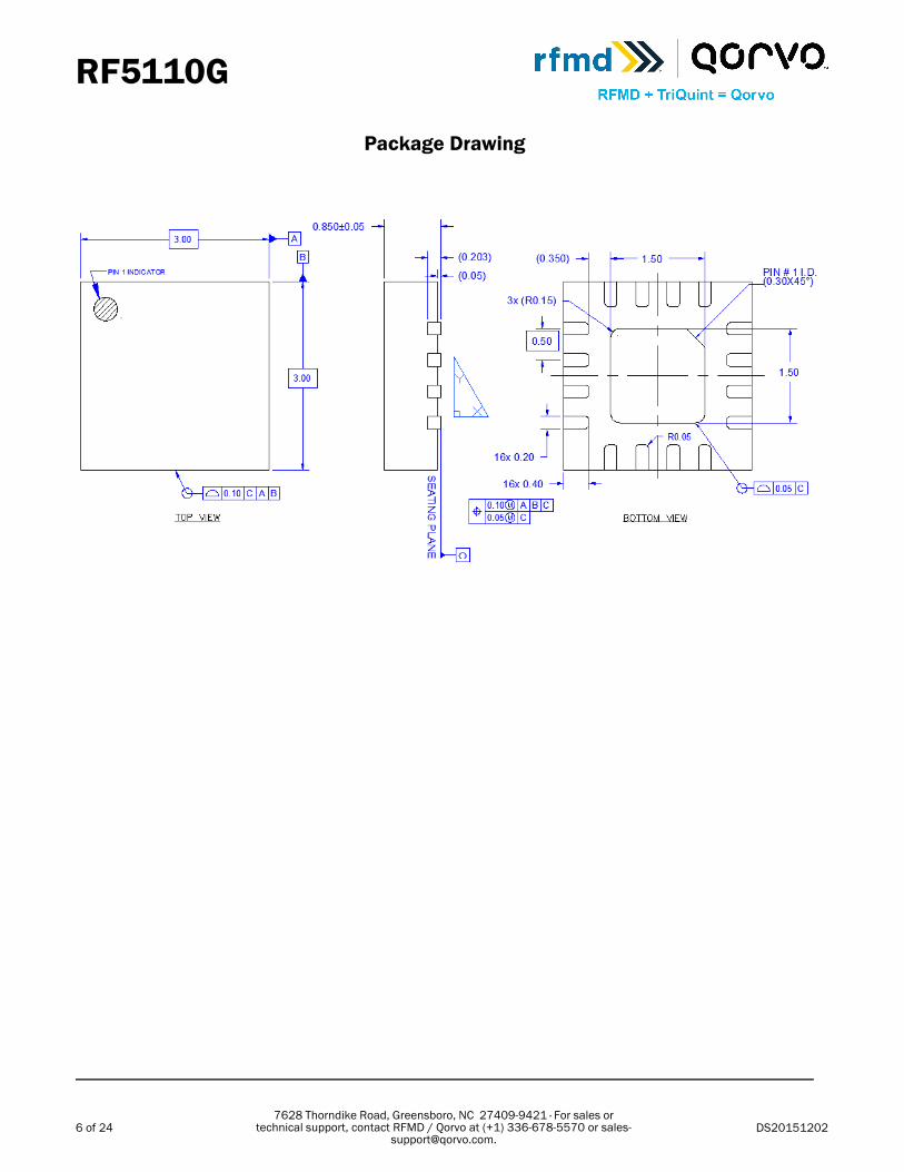
Package Drawing
7 of 24
RF5110G
DS201512027628 Thorndike Road, Greensboro, NC 27409-9421 · For sales or
technical support, contact RFMD / Qorvo at (+1) 336-678-5570 or [email protected].
Theory of Operation
General Purpose Radio ApplicationsRF5110G has seen widespread use in GSM handset applications, but it can also be used as a final transmit PA for general pur-pose radio (FSK, ASK). The application schematics in this data sheet outline matching for commonly used frequency bands.Matching is shown for 150MHz, 220MHz, 450MHz, and 865MHz to 928MHz. The standard 900MHz GSM evaluation boardcan be easily converted for these bands, using the values indicated. The 865MHZ to 928MHz conversion is the most direct,with adjustment required only on output match. The others show changes at input, 1st interstage, 2nd interstage, and output.Common components can be used in most cases. The only key component is the choke seen on RF output. During develop-ment of the matches, one goal was to achieve stability (no spurious) into 5:1 output VSWR. The 1H value and constructionproved essential in achieving this level of stability.
This Theory of Operation applies to an open loop system utilizing no power control. In the traditional GSM application, power issampled at the RF5110G’s output and fed back to a log detect function. DAC voltage (VSET) is also input to the log detector. Logdetector output drives the VAPC pin of RF5110G such that output power corresponding to VSET is obtained, with constant inputpower>0dBm applied. Power can be set over the full range of defined levels, ranging from small signal to compression. Inaddition, the control loop is used for ramping in accordance with GSM specifications. If power control is used in the systemunder consideration, most of the open loop constraints covered here will not apply, aside from thermal considerations dis-cussed below.
When used in an open loop system, RF5110G should be operated in compression. When running small signal, some variationin gain (and therefore output power) will be seen over temperature extremes between -40C and 85C. When operated in com-pression, the impact of this variation is substantially mitigated, making open loop application practical. “Compression” in thiscase is defined where efficiency exceeds 45%. In the graph section of this data sheet, curves in each frequency band areshown for gain/efficiency/junction temperature versus POUT/VCC. As indicated in the graphs, high efficiency can be obtained atcompressed output power with appropriate choice of supply voltage (VCC). For example, see the efficiency curves for 450MHz.Operation at 31dBm shows efficiency=49% for VCC=2.8V. If 32dBm output is required in design, using VCC=3.3V gives 47%efficiency. So, the system designer can choose an appropriate supply voltage which provides high efficiency at target POUT.
One important detail to consider is voltage level at VAPC. As noted earlier, VAPC level varies when operating within a power con-trol loop. This voltage controls output power from the PA. In open loop mode, VAPC should be set at 2.8V to ensure consistentoutput power from RF5110G in volume production.
Another design consideration is maintaining acceptable junction temperature. In the GSM radio, output power in excess of34dBm is common. This is allowable due to the limit on transmit duty cycle and pulse width. The worst case condition seesduty cycle at 50%, with pulse width equal to approximately 2msec. In this situation, the PA cuts off before junction temperaturereaches the maximum that would be seen with longer pulse width. For the non–GSM radio, it is assumed pulse width willexceed 2msec. Thus, restrictions must be imposed on allowable maximum output power. The most conservative analysis isused, that for 100% duty cycle. Thermal scans have shown RTH (thermal resistance) of RF5110G+the evaluation board to be36C/W. RTH for the evaluation board has been calculated at 10.4C/W, giving RF5110G RTH_JC=25.6C/W. Data sheetcurves show projected junction temperatures (TJ) for each general purpose radio frequency band. RTH of RF5110G+the evalu-ation board is taken into account. A conservative goal is TJ150C when operating at a maximum specified ambient tempera-ture of 85C. Maximum output power will then be bounded by that limit. Observing the TJ curves in bands from 150MHz to928MHz, one sees that 32dBm is always at or below 150C. This shows that the output load line in each match was intention-ally set for high efficiency. To ensure equivalent performance in one’s system, care should be taken to achieve efficiency equalto or better than that seen in the data. Thermal performance can be predicted with a simple calculation at a desired outputpower:
P_DC=VCCxICC
POUT (Watt)=[10^(POUT (dBm)/10)]/1000

8 of 24
RF5110G
DS201512027628 Thorndike Road, Greensboro, NC 27409-9421 · For sales or
technical support, contact RFMD / Qorvo at (+1) 336-678-5570 or [email protected].
Dissipated Power=PDISS=P_DC–POUT
RTH=RTH_JC_RF5110G+RTH_SYSTEM_BOARD (RTH_JC_RF5110G=25.6C/W)
Junction Temperature @ 85C ambient=TJ=85C+PDISSxRTH
Efficiency calculation alone may not suffice, as the system board may be substantially thicker than that of the RF5110G evalu-ation board. This will increase RTH for the system, and likewise TJ.
Layout considerations are important in repeating RF5110G evaluation board performance in a system design. Via arrange-ment underneath the part is critical, as are other via arrangements and supply trace routings (see “GSM Applications” sectionfor the GSM case). Layout files for the RF5110G evaluation board can be obtained by contacting RFMD applications/sales.
As already stated, output match is a primary consideration in achieving desired performance. In moving from the RF5110Gevaluation board to the system board, the first approach would be to implement the same matching topology/values as seen inapplication schematics. Performance on the system board can then be checked, particularly with regard to gain and efficiencyat target output power. If needed, matching values can be adjusted to obtain equivalent performance. Observing each outputmatch from 150MHz to 900MHz, it can be seen that topology takes 1 of 2 possible configurations:
C – L – C: 150MHz, 220MHz, 900MHz
L – C: 450MHz
Other areas which impact response are the 1st and 2nd interstage matches, found at pins 1 and 5/6, respectively. Small sig-nal responses for each match are shown in this data sheet. Checking response on the system board will verify that input/inter-stage matches are in line (output to some extent as well). This verification can be done by placing SMA connectors at theinput/output of RF5110G, and observing small signal response.
Following the guidelines contained within this section should ensure successful implementation of RF5110G in general radioapplications.
GSM ApplicationsThe RF5110G is a three-stage device with 32 dB gain at full power. Therefore, the drive required to fully saturate the output is+3dBm. Based upon HBT (Heterojunction Bipolar Transistor) technology, the part requires only a single positive 3V supply tooperate to full specification. Power control is provided through a single pin interface, with a separate Power Down control pin.The final stage ground is achieved through the large pad in the middle of the backside of the package. First and second stagegrounds are brought out through separate ground pins for isolation from the output. These grounds should be connecteddirectly with vias to the PCB ground plane, and not connected with the output ground to form a so called “local ground plane”on the top layer of the PCB. The output is brought out through the wide output pad, and forms the RF output signal path.
The amplifier operates in near Class C bias mode. The final stage is “deep AB”, meaning the quiescent current is very low. Asthe RF drive is increased, the final stage self-biases, causing the bias point to shift up and, at full power, draws about 2000mA.The optimum load for the output stage is approximately 2.6. This is the load at the output collector, and is created by theseries inductance formed by the output bond wires, vias, and microstrip, and 2 shunt capacitors external to the part. The opti-mum load impedance at the RF Output pad is 2.6-j1.5 With this match, a 50 terminal impedance is achieved. The input isinternally matched to 50 with just a blocking capacitor needed. This data sheet defines the configuration for GSM operation.
The input is DC coupled; thus, a blocking cap must be inserted in series. Also, the first stage bias may be adjusted by a resis-tive divider with high value resistors on this pin to VPC and ground. For nominal operation, however, no external adjustment isnecessary as internal resistors set the bias point optimally.
VCC1 and VCC2 provide supply voltage to the first and second stage, as well as provides some frequency selectivity to tune tothe operating band. Essentially, the bias is fed to this pin through a short microstrip. A bypass capacitor sets the inductanceseen by the part, so placement of the bypass cap can affect the frequency of the gain peak. This supply should be bypassedindividually with 100pF capacitors before being combined with VCC for the output stage to prevent feedback and oscillations.

9 of 24
RF5110G
DS201512027628 Thorndike Road, Greensboro, NC 27409-9421 · For sales or
technical support, contact RFMD / Qorvo at (+1) 336-678-5570 or [email protected].
The RF OUT pin provides the output power. Bias for the final stage is fed to this output line, and the feed must be capable ofsupporting the approximately 2A of current required. Care should be taken to keep the losses low in the bias feed and outputcomponents. A narrow microstrip line is recommended because DC losses in a bias choke will degrade efficiency and power.
While the part is safe under CW operation, maximum power and reliability will be achieved under pulsed conditions. The datashown in this data sheet is based on a 12.5% duty cycle and a 600s pulse, unless specified otherwise.
The part will operate over a 3.0V to 5.0V range. Under nominal conditions, the power at 3.5V will be greater than +34.5dBm at+90°C. As the voltage is increased, however, the output power will increase. Thus, in a system design, the ALC (AutomaticLevel Control) Loop will back down the power to the desired level. This must occur during operation, or the device may be dam-aged from too much power dissipation. At 5.0V, over +38dBm may be produced; however, this level of power is not recom-mended, and can cause damage to the device.
The HBT breakdown voltage is >20V, so there are no issue with overvoltage. However, under worst-case conditions, with the RFdrive at full power during transmit, and the output VSWR extremely high, a low load impedance at the collector of the outputtransistors can cause currents much higher than normal. Due to the bipolar nature of the devices, there is no limitation on theamount of current de device will sink, and the safe current densities could be exceeded.
High current conditions are potentially dangerous to any RF device. High currents lead to high channel temperatures and mayforce early failures. The RF5110G includes temperature compensation circuits in the bias network to stabilize the RF transis-tors, thus limiting the current through the amplifier and protecting the devices from damage. The same mechanism works tocompensate the currents due to ambient temperature variations.
To avoid excessively high currents it is important to control the VAPC when operating at supply voltages higher than 4.0V, suchthat the maximum output power is not exceeded.

10 of 24
RF5110G
DS201512027628 Thorndike Road, Greensboro, NC 27409-9421 · For sales or
technical support, contact RFMD / Qorvo at (+1) 336-678-5570 or [email protected].
Internal Schematic
RF IN
1.0 k
VCC1
PKG BASE
4.5 pF
GND2
APC1
400
VCC
VCC2 RF OUT
APC2
300
VCC
PKG BASE
5
5
APC1

11 of 24
RF5110G
DS201512027628 Thorndike Road, Greensboro, NC 27409-9421 · For sales or
technical support, contact RFMD / Qorvo at (+1) 336-678-5570 or [email protected].
Application Schematic150MHz FM Band
Application Schematic220MHz FM Band
10 nF
100 pF
180 C112
56 pF
100 pF
1 nF
1 H1
Taiyo YudenNR3012T1R0N
16 15 14 13
12
11
10
9
1
2
3
4
5 6 7 8
10 nF
8.2 nH27 pF1 nF
VCC1
VCC233 nH
10 nF
L415 nH
10 nF
1 nF
RF OUT
RF IN
VCCVCCVAPCVAPC
47 pF
0
1Requires layout change to standard evaluation board.2C11 adjacent to L4.
3.3 F+
3.3 F
+
50 mils
C1033 pF
27 pF
10 nF
100 pF
180 C102
33 pFC113
39 pF
100 pF
1 nF16 15 14 13
12
11
10
9
1
2
3
4
5 6 7 8
10 nF
8.2 nH27 pF1 nF
VCC1
VCC233 nH0
10 nF
10 nH
10 nF
1 nF
RF OUTRF IN
VCCVCCVAPCVAPC
47 pF
1Requires layout change to standard evaluation board.2C10 is adjacent to L4.3C11 is 140 mils from L4.
1 H1
Taiyo YudenNR3012T1R0N
3.3 F
+
3.3 F+
27 pF

12 of 24
RF5110G
DS201512027628 Thorndike Road, Greensboro, NC 27409-9421 · For sales or
technical support, contact RFMD / Qorvo at (+1) 336-678-5570 or [email protected].
Application Schematic450MHz FM Band
10 nF
56 pF
180 C1122 pF
56 pF
47 pF
1 nF
1 H1
Taiyo YudenNR3012T1R0N
16 15 14 13
12
11
10
9
1
2
3
4
5 6 7 8
10 nF
330 pF1 nF
VCC1
330 pF
VCC26.8 nH
10 nF
L42.7 nH
10 nF
1 nF
RF OUT
3.3 F+
RF IN
VCCVCCVAPCVAPC
3.3 F
+
47 pF
C11 adjacent to L4.
1Requires layout change to standard evaluation board.
18
0
2 pF

13 of 24
RF5110G
DS201512027628 Thorndike Road, Greensboro, NC 27409-9421 · For sales or
technical support, contact RFMD / Qorvo at (+1) 336-678-5570 or [email protected].
Application Schematic865MHz and 902MHz to 928MHz ISM Bands
10 nF
56 pF
180 C1015 pF
1 nF16 15 14 13
12
11
10
9
1
2
3
4
5 6 7 8
10 nF
11 nH27 pF1 nF
VCC1
VCC21.6 nH10 ?Ferrite
10 nF
10 nF
1 nF
RF OUTRF IN
VCCVCCVAPCVAPC
47 pF
8.8 nH
3.3 F
+
3.3 F+
15 pF 27 pF 27 pF
1.5 pFC10 and C11 are adjacent to L4.
55 mils
C115 pF
L43.6 nH 56 pF
47 pF
Share the same pad.

14 of 24
RF5110G
DS201512027628 Thorndike Road, Greensboro, NC 27409-9421 · For sales or
technical support, contact RFMD / Qorvo at (+1) 336-678-5570 or [email protected].
Application SchematicGSM850 Lumped Element
C1710 nF
C156 pF
R1180
J1RF IN
50 strip
VAPC
C915 pF
C102 pF
C119.1 pF
C1256 pF
J2RF OUT
VCC
C1433 pF
C131 nF
L38.8 nH
50 strip
16 15 14 13
12
11
10
9
1
2
3
4
5 6 7 8
C1610 nF
C1533 pF
VCCJ3
VAPC
50 strip
C81.5 pF
L111 nH
C1927 pF
C31 nF
VCC1
C733 pF
C2013 pF
VCC2
L61.6 nH
L210 Ferrite
C510 nF
L41.8 nH
C210 nF
C61 nF
65 mils 40 mils
P1
1
2
3
4
CON4
P1-1 VCC
P1-2 VCC
GND
GND
P2
1
2
3
CON3
P2-1 VAPC
GND
GND
C9 and C10 share the same pad.
60 mils
C213.3 F
+
C183.3 F
+

15 of 24
RF5110G
DS201512027628 Thorndike Road, Greensboro, NC 27409-9421 · For sales or
technical support, contact RFMD / Qorvo at (+1) 336-678-5570 or [email protected].
Evaluation Board SchematicGSM900 Lumped Element
C1710 nF
C156 pF
R1180
J1RF IN
50 strip
VAPC
VCC
C1447 pF
L38.8 nH
16 15 14 13
12
11
10
9
1
2
3
4
5 6 7 8
C1610 nF
C1547 pF
VCCJ3
VAPC
50 strip
C81.5 pF
L111 nH
C1927 pF
C31 nF
VCC1
C2327 pF
C2015 pF
VCC2
L61.6 nH
L210 Ferrite
C510 nF
C213.3 F
+
C183.3 F
+
C727 pF
P1
1
2
3
4
CON4
P1-1 VCC
P1-2 VCC
GND
GND
P2
1
2
3
CON3
P2-1 VAPC
GND
GND
C915 pF
C1011 pF
C11*5.6 pF
C1256 pF
J2RF OUT
50 strip
L43.6 nH
39 mils
*C11 is adjacent to L4.C9 and C10 share
the same pad.
C23 and C27 share the same pad.
C210 nF
C61 nF
C131 nF
55 mils

16 of 24
RF5110G
DS201512027628 Thorndike Road, Greensboro, NC 27409-9421 · For sales or
technical support, contact RFMD / Qorvo at (+1) 336-678-5570 or [email protected].
Evaluation Board LayoutBoard Size 2.0” x 2.0”
Board Thickness 0.032”; Board Material FR-4; Multi-Layer

17 of 24
RF5110G
DS201512027628 Thorndike Road, Greensboro, NC 27409-9421 · For sales or
technical support, contact RFMD / Qorvo at (+1) 336-678-5570 or [email protected].
Typical Test Setup
Notes about testing the RF5110GThe test setup shown above includes two attenuators. The 3dB pad at the input is to minimize the effect on the signal genera-tor as a result of switching the input impedance of the PA. When VAPC is switched quickly, the resulting input impedancechange can cause the signal generator to vary its output signal, either in output level or in frequency. Instead of an attenuatoran isolator may also be used. The attenuator at the output is to prevent damage to the spectrum analyzer, and should be sizedaccordingly to handle the power.
It is important not to exceed the rated supply current and output power. When testing the device at higher than nominal supplyvoltage, the VAPC should be adjusted to avoid the output power exceeding +36dBm. During load-pull testing at the output it isimportant to monitor the forward power through a directional coupler. The forward power should not exceed +36dBm, andVAPC needs to be adjusted accordingly. This simulates the behavior for the power control loop. To avoid damage, it is recom-mended to set the power supply to limit the current during the burst not to exceed the maximum current rating.
Power Supply
10dB/5W3dB
RF GeneratorSpectrumAnalyzer
Bufferx1 OpAmp
Pulse Generator
A buffer amplifier is recommended because the current into the VAPC
changes with voltage. As an alternative, the voltage may be monitored with an oscilloscope.
V+V- S-S+
18 of 24
RF5110G
DS201512027628 Thorndike Road, Greensboro, NC 27409-9421 · For sales or
technical support, contact RFMD / Qorvo at (+1) 336-678-5570 or [email protected].
PCB Design Requirements
PCB Surface FinishThe PCB surface finish used for RFMD’s qualification process is electroless nickel, immersion gold. Typical thickness is 3inchto 8inch gold over 180inch nickel.
PCB Land Pattern RecommendationPCB land patterns are based on IPC-SM-782 standards when possible. The pad pattern shown has been developed and testedfor optimized assembly at RFMD; however, it may require some modifications to address company specific assembly pro-cesses. The PCB land pattern has been developed to accommodate lead and package tolerances.
PCB Metal Land Pattern
A = 0.64 x 0.28 (mm) Typ.B = 0.28 x 0.64 (mm) Typ.C = 1.50 (mm) Sq.
BBBB
A
A
A
A
BBBB
A
A
A
A
C
Pin 16
Pin 1 Pin 12
Pin 8
Dimensions in mm.
0.50 Typ.
1.50 Typ.
0.50 Typ.
0.55 Typ.
0.55 Typ.
0.75 Typ.
0.75 Typ.1.50Typ.
Figure 1. PCB Metal Land Pattern (Top View)

19 of 24
RF5110G
DS201512027628 Thorndike Road, Greensboro, NC 27409-9421 · For sales or
technical support, contact RFMD / Qorvo at (+1) 336-678-5570 or [email protected].
PCB Solder Mask PatternLiquid Photo-Imageable (LPI) solder mask is recommended. The solder mask footprint will match what is shown for the PCBmetal land pattern with a 2mil to 3mil expansion to accommodate solder mask registration clearance around all pads. Thecenter-grounding pad shall also have a solder mask clearance. Expansion of the pads to create solder mask clearance can beprovided in the master data or requested from the PCB fabrication supplier.
Thermal Pad and Via DesignThe PCB land pattern has been designed with a thermal pad that matches the die paddle size on the bottom of the device.
Thermal vias are required in the PCB layout to effectively conduct heat away from the package. The via pattern has beendesigned to address thermal, power dissipation and electrical requirements of the device as well as accommodating routingstrategies.
The via pattern used for the RFMD qualification is based on thru-hole vias with 0.203mm to 0.330mm finished hole size on a0.5mm to 1.2mm grid pattern with 0.025mm plating on via walls. If micro vias are used in a design, it is suggested that thequantity of vias be increased by a 4:1 ratio to achieve similar results.
A = 0.74 x 0.38 (mm) Typ.B = 0.38 x 0.74 (mm) Typ.C = 1.60 (mm) Sq.
Dimensions in mm.
1.50 Typ.
0.50 Typ.
0.50 Typ.
0.55 Typ.
0.55 Typ.
0.75 Typ.
0.75 Typ. 1.50
Typ.
Pin 16
Pin 1 Pin 12
Pin 8
B B B B
A
A
A
A
BBBB
A
A
A
A
C
Figure 2. PCB Solder Mask Pattern (Top View)

20 of 24
RF5110G
DS201512027628 Thorndike Road, Greensboro, NC 27409-9421 · For sales or
technical support, contact RFMD / Qorvo at (+1) 336-678-5570 or [email protected].
RF5110G 153 MHz Gain and Efficiency Versus POUT/VCC
20
22
24
26
28
30
32
34
36
38
40
27.5 28.0 28.5 29.0 29.5 30.0 30.5 31.0 31.5 32.0 32.5
POUT (dBm)
Ga
in (
dB
)
30
35
40
45
50
55
60
65
70
75
80
Effi
cie
ncy
(%
)
153 MHz gain 3.6 V153 MHz gain 3.3 V153 MHz gain 3.0 V153 MHz eff 3.6 V153 MHz eff 3.3 V153 MHz eff 3.0 V
RF5110G 153 MHz Junction Temperature Versus POUT/VCC
Ambient Temperature = 85°C
120
122
124
126
128
130
132
134
136
138
140
142
27.5 28.0 28.5 29.0 29.5 30.0 30.5 31.0 31.5 32.0 32.5
POUT (dBm)
Jun
ctio
n T
em
pe
ratu
re (
°C)
153 MHz 3.6 V
153 MHz 3.3 V
153 MHz 3.0 V
RF5110G 220 MHz Gain and Efficiency Versus POUT/VCC
25
27
29
31
33
35
37
39
41
43
45
47
49
26 27 28 29 30 31 32 33 34 35
POUT (dB)
Ga
in (
dB
)
0
5
10
15
20
25
30
35
40
45
50
55
60
Effi
cie
ncy
(%
)
2.8 V gain3.3 V gain3.6 V gain2.8 V eff3.3 V eff3.6 V eff
RF5110G 220 MHz Junction Temperature Versus POUT/VCC
Ambient Temperature = 85°C
100
105
110
115
120
125
130
135
140
145
150
155
160
26 27 28 29 30 31 32 33 34 35
POUT (dBm)
TJ
(°C
)
2.8 V
3.3 V
3.6 V

21 of 24
RF5110G
DS201512027628 Thorndike Road, Greensboro, NC 27409-9421 · For sales or
technical support, contact RFMD / Qorvo at (+1) 336-678-5570 or [email protected].
RF5110G 865 MHz to 928 MHz Gain and Efficiency Versus POUT/VCC
27
28
29
30
31
32
33
34
35
36
37
38
39
40
27 28 29 30 31 32 33 34
PIN (dBm)
Ga
in (
dB
)
10
15
20
25
30
35
40
45
50
55
Effi
cie
ncy
(%
)
865 MHz gain 2.8V
928 MHz gain 2.8V
865 MHz gain 3.3V
928 MHz gain 3.3V
865 MHz gain 3.6V
928 MHz gain 3.6V
865 MHz eff 2.8V
928 MHz eff 2.8V
865 MHz eff 3.3V
928 MHz eff 3.3V
865 MHz eff 3.6V
928 MHz eff 3.6V
RF5110G 865 MHz to 928 MHz Junction Temperature Versus POUT/VCC
Ambient Temperature = 85°C
120
122
124
126
128
130
132
134
136
138
140
142
144
146
148
150
152
154
156
158
160
27 28 29 30 31 32 33 34
PIN (dBm)
TJ
(°C
)
2.8V 865 MHz
2.8V 928 MHz
3.3V 865 MHz
3.3V 928 MHz
3.6V 865 MHz
3.6V 928 MHz
RF5110G 450 MHz Gain and Efficiency Versus POUT/VCC
28
30
32
34
36
38
40
42
44
46
48
26 27 28 29 30 31 32 33 34 35
POUT (dBm)
Ga
in (
dB
)
0
5
10
15
20
25
30
35
40
45
50
55
60
Effi
cie
ncy
(%
)
2.8 V gain3.3 V gain2.8 V eff3.3 V eff
RF5110G 450 MHz Junction Temperature Versus POUT/VCC
Ambient Temperature = 85°C
128
130
132
134
136
138
140
142
144
146
148
150
152
154
156
158
26 27 28 29 30 31 32 33 34 35
POUT (dBm)
TJ
(°C
)
2.8 V
3.3 V
22 of 24
RF5110G
DS201512027628 Thorndike Road, Greensboro, NC 27409-9421 · For sales or
technical support, contact RFMD / Qorvo at (+1) 336-678-5570 or [email protected].
Application Schematic Small Signal Response
23 of 24
RF5110G
DS201512027628 Thorndike Road, Greensboro, NC 27409-9421 · For sales or
technical support, contact RFMD / Qorvo at (+1) 336-678-5570 or [email protected].
Tape and Reel Information
Carrier tape basic dimensions are based on EIA481. The pocket is designed to hold the part for shipping and loading onto SMTmanufacturing equipment, while protecting the body and the solder terminals from damaging stresses. The individual pocketdesign can vary from vendor to vendor, but width and pitch will be consistent.
Carrier tape is wound or placed onto a shipping reel either 330 mm (13 inches) in diameter or 178 mm (7 inches) in diameter.The center hub design is large enough to ensure the radius formed by the carrier tape around it does not put unnecessarystress on the parts.
Prior to shipping, moisture sensitive parts (MSL level 2a-5a) are baked and placed into the pockets of the carrier tape. A covertape is sealed over the top of the entire length of the carrier tape. The reel is sealed in a moisture barrier, ESD bag, which isplaced in a cardboard shipping box. It is important to note that unused moisture sensitive parts need to be resealed in themoisture barrier bag. If the reels exceed the exposure limit and need to be rebaked, most carrier tape and shipping reels arenot rated as bakeable at 125°C. If baking is required, devices may be baked according to section 4, table 4-1, column 8 ofJoint Industry Standard IPC/JEDEC J-STD-033A.
The following table provides useful information for carrier tape and reels used for shipping the devices described in this docu-ment.
QFN (Carrier Tape Drawing with Part Orientation)
RFMD Part NumberReel
Diameter Inch (mm)
Hub Diameter Inch (mm)
Width (mm)
Pocket Pitch(mm)
FeedUnits per
Reel
RF5110GTR7 7 (178) 2.4 (61) 12 4 Single 2500
Notes:
1. All dimensions are in millimeters (mm).2. Unless otherwise specified, all dimension tolerances per EIA-481.
Ao = 3.18 ± 0.10Bo = 3.18 ± 0.10F = 5.50 ± 0.05Ko = 1.02 ± 0.10P = 4.00 ± 0.10W = 12.00 +0.30/-0.10
Ø1.50±.10
15 inch Trailer Top View 15 inch Leader
Sprocket holes towardrear of reel
Pin 1Location
RFPart NumberTrace Code
RFPart NumberTrace Code
RFPart NumberTrace Code
RFPart NumberTrace Code
RFPart NumberTrace Code
RFPart NumberTrace Code
RFPart NumberTrace Code
2.00 ± 0.05
4.00 ± 0.10
FW
1.75±0.10
Bo
KoP Ao
0.279±.020
Direction of Feed

24 of 24
RF5110G
DS201512027628 Thorndike Road, Greensboro, NC 27409-9421 · For sales or
technical support, contact RFMD / Qorvo at (+1) 336-678-5570 or [email protected].
RoHS Compliant: Yes
Package total weight in grams (g): 0.021
Compliance Date Code: N/A
Bill of Materials Revision: A
Pb Free Category: e3
Pb Cd Hg Cr VI PBB PBDE
Die 0 0 0 0 0 0
Molding Compound 0 0 0 0 0 0
Lead Frame 0 0 0 0 0 0
Die Attach Epoxy 0 0 0 0 0 0
Wire 0 0 0 0 0 0
Solder Plating 0 0 0 0 0 0
* DIRECTIVE 2002/95/EC OF THE EUROPEAN PARLIAMENT AND OF THE COUNCIL of 27 January 2003 on the restriction of the use ofcertain hazardous substances in electrical and electronic equipment
RoHS* Banned Material Content
Bill of MaterialsParts Per Million (PPM)
This RoHS banned material content declaration was prepared solely on information, including analytical data, provided to RFMD by its suppliers, and applies to the Bill of Materials (BOM) revision noted above.