Embed Size (px)
Citation preview
Packaging Ma1311
PartE|53
53. Packaging Materials
Darrel Frear
This chapter is a high-level overview of the ma-terials used in an electronic package including:metals used as conductors in the package; ceram-ics and glasses used as dielectrics or insulators;and polymers used as insulators and, in a com-posite form, as conductors. There is a need fornew materials to meet the ever-changing require-ments for high-speed digital and radio frequency(RF) applications. There are different requirementsfor digital and RF packages that translate into theneed for unique materials for each application. Theinterconnecting and dielectric (insulating) require-ments are presented for each application and therelevant material properties and characteristics arediscussed. The fundamental material characteris-tics of materials are: dielectric constant, dielectricloss, thermal and electric conductivity, resistivity,moisture absorption, glass transition temperature,strength, time-dependent deformation (creep),and fracture toughness. The material character-istics and properties are dependent upon howthey are processed to form the electronic package,so the fundamentals of electronic packaging pro-cesses are discussed including wirebonding, solderinterconnects, flip chip interconnects, underfill forflip chip and overmolding. The relevant mate-rial properties are given along with requirements(including environmentally friendly Pb-free pack-ages) that require new materials to be developedto meet future electronics needs for both digitaland RF applications.
53.1 Package Applications ....................... 131253.2 The Materials Challenge
of Electronic Packaging .................... 131353.2.1 Materials Issues in High-Speed
Digital Packaging. ............................. 131353.2.2 RF Packaging Materials Issues ............ 131453.3 Materials Coefficient of Thermal
Expansion ....................................... 131553.4 Wirebond Materials ......................... 131553.4.1 Wirebond for Digital Applications ...... 131553.4.2 Wirebond for RF ............................... 131753.5 Solder Interconnects ........................ 131753.5.1 Flip Chip Interconnects ..................... 131953.5.2 Flip Chip for RF................................. 132053.5.3 Pb-Free ........................................... 132053.6 Substrates ....................................... 132253.6.1 RF Substrate Materials ...................... 132253.7 Underfill and Encapsulants .............. 132353.7.1 Underfill.......................................... 132353.7.2 Encapsulation .................................. 132353.8 Electrically Conductive Adhesives
(ECAs) .............................................. 132453.8.1 Adhesive Polymers ........................... 132453.8.2 Metal Fillers ..................................... 132553.8.3 Conduction Mechanisms ................... 132553.8.4 Isotropic Versus Anisotropic
Conduction ...................................... 132653.8.5 Rework............................................ 132653.9 Thermal Issues ................................ 132653.9.1 Thermal Issues in Digital Packaging. ... 132653.9.2 Thermal Issues in RF Packaging. ......... 132753.10 Summary ........................................ 1327References ................................................... 1327
An electronic package is a configuration of materi-als that interconnects electronic signals from one areato another. This scheme must isolate these signals sothat there is no interference and must also protect theelectronics from a degrading environment. A packagetypically consists of the semiconductor mounted andinterconnected (with solder or Au or Cu wires) to a di-electric substrate (with a leadframe or with metal traces)
that is encapsulated to seal the device from the environ-ment. The electronic package must serve four functions:
1. Provide electrical (or photonic) contact to and fromthe chip
2. Act as an electrical space transformer to take elec-tronic functionality from the dense surface of thechip to the coarser pitched outside world
© Springer International Publishing AG 2017S. Kasap, P. Capper (Eds.), Springer Handbook of Electronic and Photonic Materials, DOI 10.1007/978-3-319-48933-9_53
PartE|53.1
1312 Part E Novel Materials and Selected Applications
3. Provide environmental isolation to the semiconduc-tor, and
4. Provide an avenue for conduction of heat away fromthe device.
In the past, advances in silicon semiconductors had lit-tle or no effect on the electronic package design orprocess. New advances in silicon devices have drivenincreases in chip speed, the device density (e.g., thenumber of transistors/mm2), and power dissipation.These changes, and those planned in the future, re-quire larger numbers of interconnects to and from thedevices, improved electrical performance, more effec-tive thermal management, software systems to designand model the assembly, and different sets of mate-rials to make these changes happen. Furthermore, thepackage is shrinking to a minimalist version of theproducts that traditionally have been called packaging.The chip and board have become a conjugate pack-aging system that must provide the traditional levelsof electrical, mechanical, thermal interfaces, and en-
vironmental protection, with the additional challengeof increased performance. Furthermore, the bound-ary between where the device ends and where thepackage begins has become blurred with passive de-vices (e.g., resistors, capacitors, etc.) in the packageand redistribution layers that act as space transform-ers on the chip. Electronic packaging is becomingone of the greatest challenges in manufacturability,performance, and reliability in advanced electronicsapplications. With the tremendous growth of wire-less telecommunication, RF applications are beginningto drive many areas of microelectronics traditionallyled by the development of the microprocessor. An in-creasingly dominant factor in RF microelectronics iselectronic packaging and the materials needed to cre-ate the package because the package materials stronglyaffect the performance of the RF electronics. Manychallenges remain for packaging of microprocessors aswell. These challenges include increased speed, num-bers of input/outputs (I/O), decreased pitch, and de-creased cost.
53.1 Package Applications
Electronic packages are divided into four levels, withthree that exist beyond the integrated circuit:
� Level 0: Semiconductor chip level (integrated cir-cuits). The materials are: the semiconductor (Si,SiGe, GaAs, etc.), metalization on the circuit (Al,Cu, Au) and interconnects on the die.� Level 1: Chip in a carrier. The die is bonded (witha conductive or nonconductive adhesive or solder)into a package carrier (substrate or leadframe) and
Polymerous mold
Gold wirebrandsSilicon die
Packagesubstrate
Lead frame
Fig. 53.1 Isometric section schematic that illustrates a pe-ripheral package showing a dual-in-line-package (DiP) thatis wirebonded
interconnected by either wirebonds or bulk conduc-tive interconnects (flip chip) or solder of conductiveadhesives. An example of a wirebonded package isshown in Fig. 53.1. Figure 53.2 is a representationof a flip chip package interconnect. The die is pro-tected either by a lid or encapsulated with a polymerovermold.� Level 2: The chip carrier mounted to a board.The package is solder, or conductive adhesive, at-tached to a circuit board. An example of a packagemounted to a board using area array interconnectsis shown in Fig. 53.2.
Silicon device
BGA substrate
Printed wiring boardBGA solder balls
Flip chipsolder balls
Underfill
Fig. 53.2 Schematic illustration of an area array packagewith a flip chip device interconnect and a ball grid arraypackage
Packaging Materials 53.2 The Materials Challenge of Electronic Packaging 1313Part
E|53.2
� Level 3: Board to board interconnects. The boardsare interconnected to the final electronic system us-
ing friction interconnects, solder interconnects, orfiber-optic connectors.
53.2 The Materials Challenge of Electronic Packaging
Electronic packaging is arguably the most materials-intensive application today. The families of materialsincluded in a package include: semiconductors, ceram-ics, glasses, composites, polymers, and metals. A list ofthe types of materials used in an electronic package isshown in Table 53.1. The processes required to assem-ble a package are equally varied: welding, soldering,curing, cold and hot working, sintering, adhesive bond-ing, laser drilling, and etching.
Each of these materials and how they are used in anelectronic package could be the topic of an entire book.This chapter is a high-level overview of the materialsused in an electronic package. The focus is on the fol-lowing classes of materials:
Table 53.1 Examples of materials used in electronic pack-aging
Semiconductors Si, SiGe, GaAsMetals Solders for interconnects (Sn-Pb, Sn-Ag,
Sn-Ag-Cu, Sn-Au, Sn-Sb)Au or Cu wirebondsCu leadframes (Kovar, CuBe, Alloy 42)Cu traces in substratesW, Mo traces in cofired ceramicsAg, Au, Pd for thin/thick films on ceramicsNi diffusion barrier metalizationsAl heat sinks
Ceramics Al2O3 substrates modified with BaO,SiO2, CuO, etc.LTCC substratesAl2O3
modified with low-temperature glass (e.g.,PbO)SiN dielectricsDiamond heat sinks
Polymers Epoxies (overmold)Filled epoxies (overmold)Silica-filled anhydride resin (underfills)Conductive adhesives (die bonding, inter-connects)Laminated epoxy/glass substratesPolyimide dielectricBenzoyclobuteneSiliconesPhotosensitive polymers for photomasks(acrylates, monomers, etc.)
Glasses SiO2 fibers for optoelectronicsSilicate glasses for sealingBorosilicate glass substratesGlass fibers for epoxy/glass substrates(FR-4)
Metals are used as conductors in the package, pri-marily electrical but also thermal for power devices.This includes the thin metal interconnects on the in-tegrated circuit made of Al, Cu or Au and the inter-connects between the integrated circuit and the packagethat are either wirebond interconnects or solder joints.Metals are also used to act as heat sinks for power de-vices and as shields for RF applications
Ceramics and glasses are used as dielectrics or in-sulators. Ceramics are used in devices as dielectrics toform capacitors and inductors. In the package itself, theceramics are used as insulating materials and as sub-strates that provide a structural base that electricallyisolates lines and pads.
Polymers are used as insulators and, in a compos-ite form, as conductors. As an insulator, polymers areencapsulants, underfills and substrates (note: in theseapplications, polymers are used as composites with sil-ica or glass fillers). Polymers are also used as insulatingadhesives to glue components to a substrate or board toprovide mechanical strength. The addition of metal par-ticles to the polymer can make it a conductive materialused as a conductive adhesive interconnect.
Composite materials are a mix of materials thatcan be tailored for either mechanical behavior im-provements, thermal enhancement or as an electricalconductor. Many of the composite materials used inpackages are based on a polymer matrix as noted in thepolymer section above.
There is a wealth of general information on materi-als in electronic packaging. Some additional resourcesare found in [53.1–8].
53.2.1 Materials Issues in High-SpeedDigital Packaging
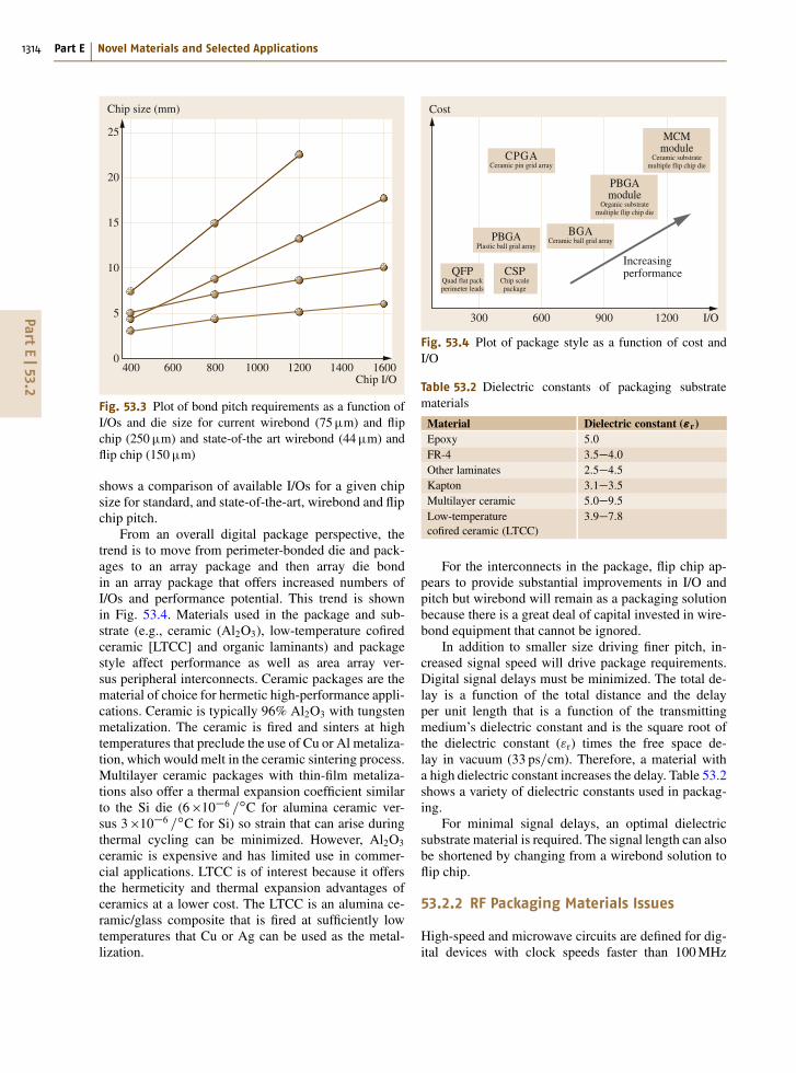
The ability to decrease line width and feature size insemiconductor technology is decreasing below 90 nm.As the feature size shrinks, the function per unit area onthe die increases. This increased functionality means ei-ther smaller die or more I/Os per die. The reduced diesize also reduces the available perimeter of the pack-age for wirebond pads while increased functionalityrequires more I/Os. The decreased perimeter area alsodrives wirebond capability down to 44�m pitch with10�m gold wire. An attractive solution to this decreas-ing size is to use the entire surface of the chip (flip chip)rather than just the periphery (wirebond). Figure 53.3
PartE|53.2
1314 Part E Novel Materials and Selected Applications
25
20
15
10
5
01600140012001000800600400
Chip size (mm)
Chip I/O
Fig. 53.3 Plot of bond pitch requirements as a function ofI/Os and die size for current wirebond (75�m) and flipchip (250�m) and state-of-the art wirebond (44�m) andflip chip (150�m)
shows a comparison of available I/Os for a given chipsize for standard, and state-of-the-art, wirebond and flipchip pitch.
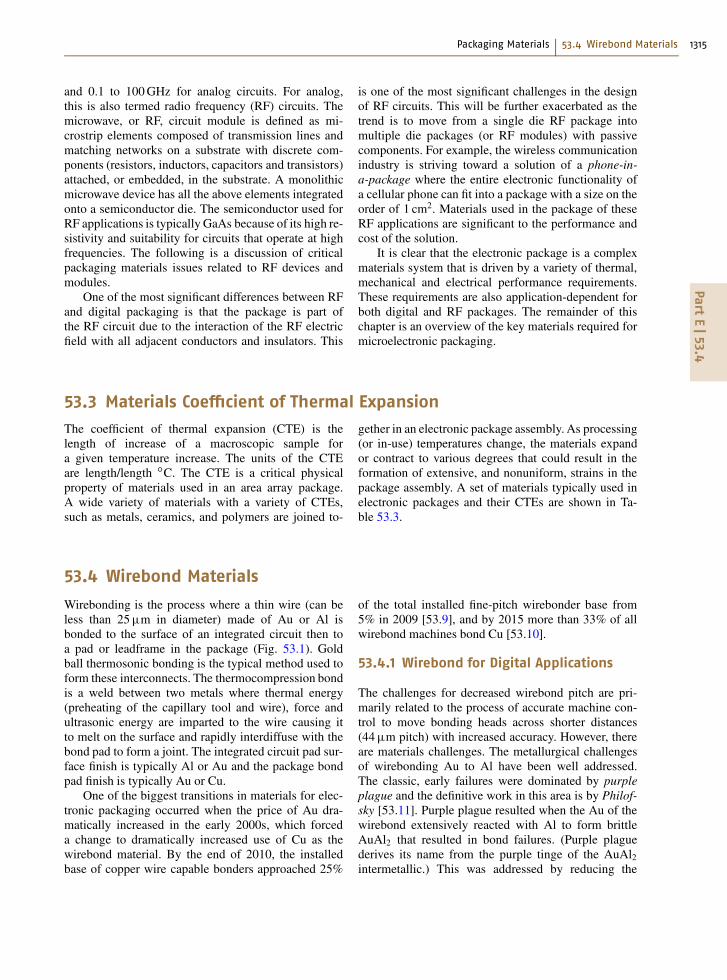
From an overall digital package perspective, thetrend is to move from perimeter-bonded die and pack-ages to an array package and then array die bondin an array package that offers increased numbers ofI/Os and performance potential. This trend is shownin Fig. 53.4. Materials used in the package and sub-strate (e.g., ceramic (Al2O3), low-temperature cofiredceramic [LTCC] and organic laminants) and packagestyle affect performance as well as area array ver-sus peripheral interconnects. Ceramic packages are thematerial of choice for hermetic high-performance appli-cations. Ceramic is typically 96% Al2O3 with tungstenmetalization. The ceramic is fired and sinters at hightemperatures that preclude the use of Cu or Al metaliza-tion, which would melt in the ceramic sintering process.Multilayer ceramic packages with thin-film metaliza-tions also offer a thermal expansion coefficient similarto the Si die (6�10�6 =ıC for alumina ceramic ver-sus 3�10�6 =ıC for Si) so strain that can arise duringthermal cycling can be minimized. However, Al2O3
ceramic is expensive and has limited use in commer-cial applications. LTCC is of interest because it offersthe hermeticity and thermal expansion advantages ofceramics at a lower cost. The LTCC is an alumina ce-ramic/glass composite that is fired at sufficiently lowtemperatures that Cu or Ag can be used as the metal-lization.
1200900600300
Cost
I/O
QFPQuad flat packperimeter leads
PBGAPlastic ball grid array
CSPChip scalepackage
BGACeramic ball grid array
CPGACeramic pin grid array
PBGAmodule
Organic substratemultiple flip chip die
MCMmodule
Ceramic substratemultiple flip chip die
Increasingperformance
Fig. 53.4 Plot of package style as a function of cost andI/O
Table 53.2 Dielectric constants of packaging substratematerials
Material Dielectric constant ("r)Epoxy 5:0FR-4 3:5�4:0Other laminates 2:5�4:5Kapton 3:1�3:5Multilayer ceramic 5:0�9:5Low-temperaturecofired ceramic (LTCC)
3:9�7:8
For the interconnects in the package, flip chip ap-pears to provide substantial improvements in I/O andpitch but wirebond will remain as a packaging solutionbecause there is a great deal of capital invested in wire-bond equipment that cannot be ignored.
In addition to smaller size driving finer pitch, in-creased signal speed will drive package requirements.Digital signal delays must be minimized. The total de-lay is a function of the total distance and the delayper unit length that is a function of the transmittingmedium’s dielectric constant and is the square root ofthe dielectric constant ("r) times the free space de-lay in vacuum (33 ps=cm). Therefore, a material witha high dielectric constant increases the delay. Table 53.2shows a variety of dielectric constants used in packag-ing.
For minimal signal delays, an optimal dielectricsubstrate material is required. The signal length can alsobe shortened by changing from a wirebond solution toflip chip.
53.2.2 RF Packaging Materials Issues
High-speed and microwave circuits are defined for dig-ital devices with clock speeds faster than 100MHz
Packaging Materials 53.4 Wirebond Materials 1315Part
E|53.4
and 0.1 to 100GHz for analog circuits. For analog,this is also termed radio frequency (RF) circuits. Themicrowave, or RF, circuit module is defined as mi-crostrip elements composed of transmission lines andmatching networks on a substrate with discrete com-ponents (resistors, inductors, capacitors and transistors)attached, or embedded, in the substrate. A monolithicmicrowave device has all the above elements integratedonto a semiconductor die. The semiconductor used forRF applications is typically GaAs because of its high re-sistivity and suitability for circuits that operate at highfrequencies. The following is a discussion of criticalpackaging materials issues related to RF devices andmodules.
One of the most significant differences between RFand digital packaging is that the package is part ofthe RF circuit due to the interaction of the RF electricfield with all adjacent conductors and insulators. This
is one of the most significant challenges in the designof RF circuits. This will be further exacerbated as thetrend is to move from a single die RF package intomultiple die packages (or RF modules) with passivecomponents. For example, the wireless communicationindustry is striving toward a solution of a phone-in-a-package where the entire electronic functionality ofa cellular phone can fit into a package with a size on theorder of 1 cm2. Materials used in the package of theseRF applications are significant to the performance andcost of the solution.
It is clear that the electronic package is a complexmaterials system that is driven by a variety of thermal,mechanical and electrical performance requirements.These requirements are also application-dependent forboth digital and RF packages. The remainder of thischapter is an overview of the key materials required formicroelectronic packaging.
53.3 Materials Coefficient of Thermal ExpansionThe coefficient of thermal expansion (CTE) is thelength of increase of a macroscopic sample fora given temperature increase. The units of the CTEare length/length ıC. The CTE is a critical physicalproperty of materials used in an area array package.A wide variety of materials with a variety of CTEs,such as metals, ceramics, and polymers are joined to-
gether in an electronic package assembly. As processing(or in-use) temperatures change, the materials expandor contract to various degrees that could result in theformation of extensive, and nonuniform, strains in thepackage assembly. A set of materials typically used inelectronic packages and their CTEs are shown in Ta-ble 53.3.
53.4 Wirebond Materials
Wirebonding is the process where a thin wire (can beless than 25�m in diameter) made of Au or Al isbonded to the surface of an integrated circuit then toa pad or leadframe in the package (Fig. 53.1). Goldball thermosonic bonding is the typical method used toform these interconnects. The thermocompression bondis a weld between two metals where thermal energy(preheating of the capillary tool and wire), force andultrasonic energy are imparted to the wire causing itto melt on the surface and rapidly interdiffuse with thebond pad to form a joint. The integrated circuit pad sur-face finish is typically Al or Au and the package bondpad finish is typically Au or Cu.
One of the biggest transitions in materials for elec-tronic packaging occurred when the price of Au dra-matically increased in the early 2000s, which forceda change to dramatically increased use of Cu as thewirebond material. By the end of 2010, the installedbase of copper wire capable bonders approached 25%
of the total installed fine-pitch wirebonder base from5% in 2009 [53.9], and by 2015 more than 33% of allwirebond machines bond Cu [53.10].
53.4.1 Wirebond for Digital Applications
The challenges for decreased wirebond pitch are pri-marily related to the process of accurate machine con-trol to move bonding heads across shorter distances(44�m pitch) with increased accuracy. However, thereare materials challenges. The metallurgical challengesof wirebonding Au to Al have been well addressed.The classic, early failures were dominated by purpleplague and the definitive work in this area is by Philof-sky [53.11]. Purple plague resulted when the Au of thewirebond extensively reacted with Al to form brittleAuAl2 that resulted in bond failures. (Purple plaguederives its name from the purple tinge of the AuAl2intermetallic.) This was addressed by reducing the
PartE|53.4
1316 Part E Novel Materials and Selected Applications
Table 53.3 Coefficients of thermal expansion of a sam-pling of materials used in area array electronic packages
Material CTE (10�6 =ıC)Metals304 Stainless Steel 17:8Ag 19:7Al 23:5Alloy 42 4:9Au 14:2Cu 16:8Invar 1:6Kovar 5:5Mo 5:1Ni 13�15Solder: 63Sn-37Pb 25Solder: 95Pb-5Sn 28Ti 10W 4:5
CeramicsAlN 4:3Alumina (96%) 6:4Alumina (99:5%) 6:5BeO 7:8BN 3:7Fused silica glass 0:56Quartz 13SiC 3:8SiN 3
SemiconductorsGaAs 5:8Si 2:7
Organic materialsEpoxy resins 50�80FR-4 (x–y plane) 15:8FR-4 (z-axis) 80�90Polycarbonates 50�70Polyimide glass (x–y plane) 12�14Polyimide glass (z-axis) 60Polyimides 40�50Polyurethanes 180�250RTV 800
wirebond process temperature to below 300 ıC, whichreduced the extent of the AuAl2 formation. Currentwirebond failures are the result of surface impuritiesor corrosion. These are addressed by plasma or ul-traviolet (UV)-ozone cleaning of the surface prior towirebond.
Wirebonding problems have also been caused byplating impurities in Au bond pads. The impurities inthe Au diffuse to the molten front that occurs duringwirebonding and concentrate in a plane in the bond. Ifthere are a sufficient number of impurities, they precipi-tate and act as sinks for vacancies that can become voidsand lower the bond strength. The impurities have been
Thermallystablezone
Heataffected
zone (HAZ)
Remeltedzone
Stablegrains
Solid-statecoarsened
grains
As solidifiedcoarse grains
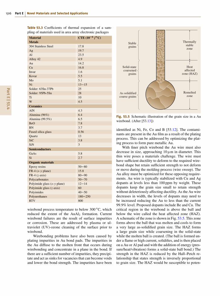
Fig. 53.5 Schematic illustration of the grain size in a Auwirebond. (After [53.13])
identified as Ni, Fe, Co and B [53.12]. The contami-nants are present in the Au film as a result of the platingprocess. This can be addressed by optimizing the plat-ing process to form pure metallic Au.
With finer pitch wirebond the Au wire must alsodecrease in size, approaching 10�m in diameter. Thisthin wire poses a materials challenge. The wire musthave sufficient ductility to deform to the required wire-bond shape but retain sufficient strength to not deformor move during the molding process (wire sweep). TheAu alloy must be optimized for these opposing require-ments. Au wire is typically stabilized with Cu and Agdopants at levels less than 100 ppm by weight. Thesedopants keep the grain size small to retain strengthwithout deleteriously affecting ductility. As the Au wiredecreases in width, the levels of dopants may need tobe increased reducing the Au to less than the current99:9% level. Proposed dopants include Be and Cu. Thecritical region in the wirebond is above the ball andbelow the wire called the heat affected zone (HAZ).A schematic of the zone is shown in Fig. 53.5. This zoneforms above the ball that was molten and cools to forma very large as-solidified grain size. The HAZ formsa large grain size while coarsening in the solid-statewhile the molten ball is created. (The ball is formed un-der a flame or high current, solidifies, and is then placedon a Au or Al pad and with the addition of energy (pres-sure/heat/vibration) forms a solid-state ball bond.) Thestrength in the HAZ is reduced by the Hall–Petch re-lationship that states strength is inversely proportionalto grain size. The HAZ would be susceptible to poten-
Packaging Materials 53.5 Solder Interconnects 1317Part
E|53.5
tially high levels of strain during molding and wouldbe the most likely failure location. In thinner wires, anincreased grain size is even more critical and alloyingelements are needed to stabilize the structure and re-tain sufficient strength without affecting the ductilityrequired to form the wirebond.
The use of Cu as the wirebond material requires sig-nificant process changes because Cu is harder than Auand oxidizes much more quickly, requiring specializedcopper wirebond process parameters (e.g., a reducingatmosphere at wirebond or higher pressure/energy atwirebond). Cu is harder and has lower ductility than Auso the bonding process window is more narrow and re-quires more effort to optimize the process so damageto the Si under the bond pad is minimized. The metal-lurgical reaction between the Cu wire and the Al bondpad is not as extensive as the Au-Sn intermetallic thatforms in Au wirebonding. The thinner intermetallic ismore stable and results in a more robust bond. The elec-trical performance of Cu is better than Au wirebonds
because copper enables better heat dissipation and cancarry more power with thinner wire diameters.
53.4.2 Wirebond for RF
At RF frequencies the wirebonds affect electrical per-formance. At sub-RF frequencies, the wirebonds canbe neglected as their resistance and inductance are inthe noise with respect to performance. In RF applica-tions, the wirebonds experience parasitic losses due toinductance with adjacent wirebonds resulting in signaldisturbance. RF circuit designers typically add at least1 nH inductance per wirebond, but the effect can bevariable and must be physically compensated by tun-ing the circuit. In effect, the wirebonds act as discreteinductors. The materials issues for RF wirebond are thesame as described above for digital, but the effect of thewirebonds themselves is significant in RF compared todigital and must be accounted for in the design of thedevice.
53.5 Solder Interconnects
For surface mount and area array applications, the roleof solder in the package is significant. In these advanceddesigns, the solder is an electrical interconnect, a me-chanical bond and must often serve as a thermal conduitto remove heat from the joined device. The intercon-nects become more critical as chip size, chip carriersize, and the number of I/Os increase, while the sol-der joint size and cost decreases. Furthermore, some ofthe use environments are becoming increasingly severe.For example, some automotive electronics are beingplaced in locations under the hood with temperature ex-tremes that could range from �55 to 180 ıC. Portabledevices, such as cellular telephones are expected towithstand severe shock environments caused by drop-ping the phone.
A solder interconnect consists of the solder alloyand the pads to which it is joined. The solder alloy isa low-temperature-melting metal that wets and reactswith metal pads or leads to form a metallurgical bond.During the wetting process the solder reacts with thepad metalization forming an intermetallic compound(IC) on the pad surface that continues to grow when thesolder is in the solid state.
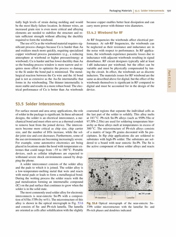
The most commonly used solder alloy for electronicinterconnects is near-eutectic Sn-Pb with a composi-tion of 63Sn-37Pb (by wt%). The microstructure of thisalloy is shown in the optical micrograph in Fig. 53.6and consists of Sn- and Pb-rich lamella. The lamellaare oriented as cells after solidification with the slightly
coarsened regions that separate the individual cells asthe last part of the solder to solidify. This alloy meltsat 183 ıC. Pb-rich Sn-Pb alloys (such as 95Pb-5Sn or97.5Pb-2.5Sn) are used for soldering temperature hier-archy as these alloys melt at temperatures in excess of300 ıC. The microstructure of Pb-rich alloys consistsof a matrix of large Pb grains decorated with Sn pre-cipitates. In flip chip applications die are soldered tosubstrates with high-Pb solder. The substrates are sol-dered to a board with near eutectic Sn-Pb. The Sn isthe active component of these solder alloys and reacts
Pb dendrites Lamellar
200 μm
Fig. 53.6 Optical micrograph of the near-eutectic Sn–37Pb solder microstructure with the lamellar Sn- andPb-rich phases and dendrites indicated
PartE|53.5
1318 Part E Novel Materials and Selected Applications
0 cycles
1300 cycles
625 cycles
2000 cycles
1000 cycles
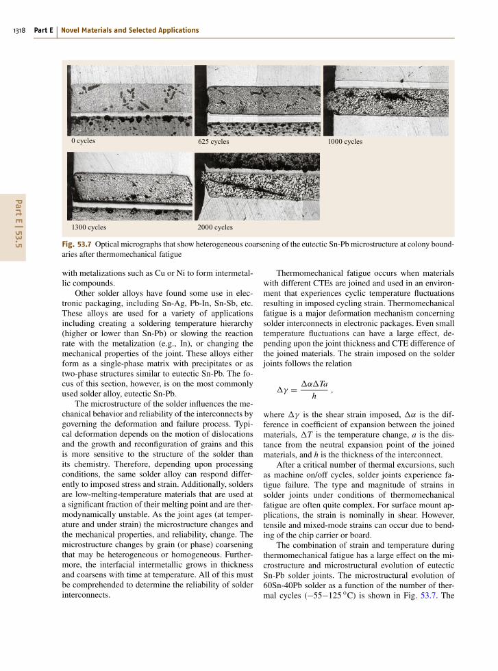
Fig. 53.7 Optical micrographs that show heterogeneous coarsening of the eutectic Sn-Pb microstructure at colony bound-aries after thermomechanical fatigue
with metalizations such as Cu or Ni to form intermetal-lic compounds.
Other solder alloys have found some use in elec-tronic packaging, including Sn-Ag, Pb-In, Sn-Sb, etc.These alloys are used for a variety of applicationsincluding creating a soldering temperature hierarchy(higher or lower than Sn-Pb) or slowing the reactionrate with the metalization (e.g., In), or changing themechanical properties of the joint. These alloys eitherform as a single-phase matrix with precipitates or astwo-phase structures similar to eutectic Sn-Pb. The fo-cus of this section, however, is on the most commonlyused solder alloy, eutectic Sn-Pb.
The microstructure of the solder influences the me-chanical behavior and reliability of the interconnects bygoverning the deformation and failure process. Typi-cal deformation depends on the motion of dislocationsand the growth and reconfiguration of grains and thisis more sensitive to the structure of the solder thanits chemistry. Therefore, depending upon processingconditions, the same solder alloy can respond differ-ently to imposed stress and strain. Additionally, soldersare low-melting-temperature materials that are used ata significant fraction of their melting point and are ther-modynamically unstable. As the joint ages (at temper-ature and under strain) the microstructure changes andthe mechanical properties, and reliability, change. Themicrostructure changes by grain (or phase) coarseningthat may be heterogeneous or homogeneous. Further-more, the interfacial intermetallic grows in thicknessand coarsens with time at temperature. All of this mustbe comprehended to determine the reliability of solderinterconnects.
Thermomechanical fatigue occurs when materialswith different CTEs are joined and used in an environ-ment that experiences cyclic temperature fluctuationsresulting in imposed cycling strain. Thermomechanicalfatigue is a major deformation mechanism concerningsolder interconnects in electronic packages. Even smalltemperature fluctuations can have a large effect, de-pending upon the joint thickness and CTE difference ofthe joined materials. The strain imposed on the solderjoints follows the relation
� D ˛ Ta
h;
where � is the shear strain imposed, ˛ is the dif-ference in coefficient of expansion between the joinedmaterials, T is the temperature change, a is the dis-tance from the neutral expansion point of the joinedmaterials, and h is the thickness of the interconnect.
After a critical number of thermal excursions, suchas machine on/off cycles, solder joints experience fa-tigue failure. The type and magnitude of strains insolder joints under conditions of thermomechanicalfatigue are often quite complex. For surface mount ap-plications, the strain is nominally in shear. However,tensile and mixed-mode strains can occur due to bend-ing of the chip carrier or board.
The combination of strain and temperature duringthermomechanical fatigue has a large effect on the mi-crostructure and microstructural evolution of eutecticSn-Pb solder joints. The microstructural evolution of60Sn-40Pb solder as a function of the number of ther-mal cycles (�55�125 ıC) is shown in Fig. 53.7. The
Packaging Materials 53.5 Solder Interconnects 1319Part
E|53.5
microstructure evolves through deformation that con-centrates at the colony boundaries closely parallel tothe direction of imposed shear strain, causing the cellsto slide or rotate relative to one another. The structurewithin the cell boundaries becomes slightly coarsenedrelative to the remaining solder-joint microstructureand, thus are the weak links of the joint. Damage (inthe form of defects or dislocations) is created at thecell boundaries at the low-temperature portion of a ther-mal cycle. As the temperature rises, the deformationis annealed by recrystallization or stress-assisted diffu-sion where material diffuses to regions of high stress.This results in coarsening the Sn-rich and Pb-rich grainsand phases in colony boundaries. The heterogeneouslycoarsened colony boundaries are weaker than the restof the joint and any further deformation concentratesin the coarsened regions resulting in further coarsen-ing. Failure eventually occurs due to cracks that form inthe coarsened regions of a joint. The first indications ofimpending failure are associated with cracking of coars-ened Sn-rich grains in the heterogeneous region whoseinitial as-solidified grain size is in the submicron range.When cracks initiate during thermomechanical fatigue,the Sn-grain size grows to a range of about 5�10�m.Failure occurs when grains can no longer slide and ro-tate to accommodate the imposed strain resulting inintergranular separation.
Lead-rich Pb-Sn alloys undergo thermomechani-cal fatigue but show little evidence of microstructuralevolution. These solders undergo intergranular failurecaused by void coalescence and growth at Pb grainboundaries. The strain imposed during thermomechani-cal fatigue cannot be accommodated by large Pb grains,resulting in intergranular failure. However, Pb loses thework-hardening effect quickly so that damage in theform of cracks does not propagate easily.
Other solder alloys, such as the Pb-free Sn-3.5Ageutectic-based solders, experience thermomechanicalfatigue damage and failure at Sn grain boundaries. Themicrostructural evolution in these alloys tends to bephase coarsening with minimal grain size coarsening.Sn-Ag-X alloys tend to have longer thermomechanicalfatigue lifetimes than near-eutectic Sn-Pb solders.
Intermetallic compounds form between pad metal-ization and the active components of the molten solder(typically Sn). For a Cu metalization, the Sn reactsto form Cu3Sn and Cu6Sn5 intermetallics. For Ni, theSn reacts to form Ni3Sn4. After solidification, the in-termetallic compounds continue to grow by solid-statediffusion. Over long periods of time, the intermetalliclayers can grow to significant thicknesses (> 20�m)and the solder–intermetallic interfaces may constituteeasy sites for crack initiation and propagation. Exces-sive growth also consumes the base metal, or finish, that
can result in the loss of adhesion to the underlyingmetalthat is not solder wettable or create a plane of weaknessowing to the stress generated from an intermetallic layerthat is too thick. The metalized pad thickness generallymust be greater than that consumed by the solder.
The transformation of solder-wettable coatings intointermetallics by solid-state reactions can also result inexcessive intermetallic growth that degrades mechani-cal properties. The interfacial intermetallics are brittleand may fracture when strain is imposed, especiallyif the strain is tensile in nature. Solder-joint interfa-cial intermetallics are brittle because they typically havecomplex crystal structures with few crystallographicplanes available to accommodate stress by strain relief,i. e., plastic deformation via a slip mechanism. The fail-ures are characteristically brittle and occur through theintermetallic or at the intermetallic/solder interface un-der low-load conditions.
53.5.1 Flip Chip Interconnects
Recent developments in the under bump metallurgy(UBM) and solder joints have resulted in lower costand higher performance flip chip interconnects. TheUBM serves as an electrical, thermal, and mechanicalinterface between the silicon bond pads and the pack-age substrate. The structure of the UBM is designed toadhere to the Al on the Si, act as a diffusion barrierbetween the solder and Si, and be a wettable surfaceto join to the solder. The most common UBM is theevaporated Cr/Cr-Cu/Cu/Au developed by IBM [53.14]for use with an evaporated high-Pb-content Pb-Sn alloyjoined to a ceramic substrate. This UBM is expensiveand new UBM systems with sputtered or plated metal-izations have been developed. Plated metalizations arethe lowest cost UBM.
A significant change in flip chip interconnects is themove toward a lower-melting-point solder alloy, suchas eutectic 63Sn-37Pb (wt%) that can be processed be-low 220 ıC as opposed to 350 ıC for high-Pb solder.New materials on the die (low-� dielectric) and sub-strate (organic materials) require this lower processingtemperature. The change in solder alloy also requiresa change in UBM. Traditional UBM systems are basedon a thin Cu layer that dissolves into high-Sn solders re-sulting in spalling and dewetting. Eutectic solder UBMsystems utilize a layer of Ni for solder wetting. The Niis wet by Sn-Pb solder but reacts much slower thanCu. The addition of � 9% V to Ni reduces the fer-romagnetic behavior of the Ni and enables the use ofsputtering of the Ni. Electroless plating of Ni-9%P isthe lowest cost UBM and has the advantage that plat-ing occurs only where desired on the metal pads onthe silicon. To plate onto Al, the pads are zincated then
PartE|53.5
1320 Part E Novel Materials and Selected Applications
immediately plated with Ni. One issue with Ni-basedUBMs is the intermetallic layer between the solder andNi (Ni3Sn4). Although very thin, this intermetallic layercan be brittle and the long-term reliability must be fullycharacterized and understood.
There are three solder deposition techniques avail-able for flip chip. Traditionally, high-Pb solder is evapo-rated onto the UBM then reflowed to form metallurgicalbonds. Evaporation is expensive because the masksmust be regularly cleaned and there is excessive scrapsolder. The composition of evaporated solder is diffi-cult to control outside the high-Pb regime. Solder pasteis a lower cost alternative to evaporation and involvesscreening the paste onto the UBM then reflowing. Sol-der paste reduces waste, cleaning is inexpensive, andthe paste comes in a variety of compositions, includ-ing eutectic Sn-Pb. The difficulty with paste arises atfine pitch applications where the rheology of the pastemakes it difficult to force into the required small holesin the screen. Solder may also be plated, which is inex-pensive (no waste and easy cleaning) and has excellentfine pitch coverage. Solder bumps of a pitch of 25mmhave been achieved by plating. The difficulty with plat-ing is achieving ball and compositional uniformity.
The trend in flip chip interconnect pitch is thatthe current 250�m pitch will continue to shrink. Thedriving force for this pitch shrink is to satisfy the re-quirements for high-performance silicon devices. Theserequirements include a dramatic increase in the numberof I/Os due to increases in the number of signal linesand power requirements. Higher power devices requiremore signal and ground lines and, to limit point sourcesof heat, the power and ground interconnects should bespread evenly across the area array.
There are a number of materials and processingchallenges associated with finer pitches. As the pitchshrinks, the methods to deposit the solder become morelimited. Solder paste is very difficult to deposit usinga silk-screen method at pitches below 150�m due torheological limitations of forcing a semisolid (the paste)into small holes (the silk screen). Evaporation is diffi-cult because developing a metal screen mask with therequired tolerances is prohibitively expensive. Solderplating is still a good option but the solder must bevery uniform across each die. Solder ball uniformity iscritical because large variations between die could re-sult in electrical opens, for small balls, and shorts, forlarge balls. At 250�m, ball uniformity across a die is10%, at 150�m this decreases to 5% and the changein dimension tolerance is 12:5�m down to 3:75�m.An additional issue with a decrease in ball size is thejoint gap between the substrate and the die decreasesto the point that it may become very difficult to flowunderfill completely under the die. At 100�m pitch the
gap between the die and substrate could be significantlyless than 25�m, below the limit of underfill flow. Forthese very fine pitch applications an alternative underfilltechnique will need to be developed because flow underthe chip will not be possible. One alternative would beto deposit the underfill material on the wafer immedi-ately after flip chip solder bumping then underfill curewould simultaneously occur during solder relfow. Newunderfill materials and processes must be developed toimplement this process.
53.5.2 Flip Chip for RF
Flip chip provides substantial improvements in off-circuit RF performance because the inductance is de-creased as the ball height and shape is very consistentand predictable. Wirebond lengths can vary (typicallyC=� 100�m) resulting in parasitic variations not ob-served in flip chip interconnects. The number of I/Oson an RF circuit is generally small so the pitch of theinterconnects is generally quite large.
The die interconnects on GaAs are typically Auwhereas on Si they are Al. A UBM is required for Siapplications because solder does not wet Al. The sol-der would wet the Au of the GaAs but the Au layer isvery thin and would dissolve the entire Au layer veryquickly so a UBM is also required for GaAs. The UBMsavailable for Si can also be applied to GaAs but can besimpler because the adhesion of other metals to Au iseasier to achieve than it is on Al.
The solder alloys for GaAs flip chip bumps tendto be similar to that for Si but with a greater empha-sis on Au-based alloys because of the desire to usea highly conductive material such as Au for very-high-speed applications. Eutectic Au-Sn, Ag and In alloyshave been commonly used but the wetting of these sol-ders is typically poor. For finer pitch applications onGaAs (due to small die size, not large numbers of I/Os)other materials with good wetting are needed. Conduc-tive adhesives have been explored for GaAs bumps.Work by Lin et al. [53.15] found no significant differ-ence in electrical performance up to 2GHz betweena conductive adhesive and Au-Sn solder. The use of un-derfill for flip chip packages can cause a major loss inRF energy because the high dielectric constant of theunderfill polymer is greater than that of air. With a con-ductive adhesive localized to just the bond pads, not theentire surface of the die, this RF loss will not be ob-served.
53.5.3 Pb-Free
The electronics industry extensively uses Pb-Sn sol-der alloys in flip chip applications as well as in many
Packaging Materials 53.5 Solder Interconnects 1321Part
E|53.5
other interconnects in the electronic package. How-ever, medical studies have shown that Pb is a heavymetal toxin that can damage the kidneys, liver, blood,and central nervous system. Less than one percent peryear of the global Pb consumption is used in solderalloys for electronic products but electronics and elec-trical systems make up an increasingly larger fractionof landfills [53.16]. The issue of Pb leaching from land-fills into the water table has raised alarm as a potentialsource of long-term contamination of soil and groundwater. Concerns about the presence of Pb in the en-vironment and potential exposure scenarios that couldresult in the ingestion of Pb by humans and wildlifehas prompted a concerted effort to limit the use ofPb in manufactured products (notably gasoline, plumb-ing solders, and paint). International laws have recentlybeen proposed to expand Pb control laws to limit orban the use of Pb in manufactured electronics prod-ucts. The most aggressive and well-known effort isthe European Union’s Waste in Electrical and Elec-tronic Equipment (WEEE) directive that proposed a banon Pb in electronics by 2006. The Japanese Environ-mental Agency has proposed that Pb-containing scrapmust be disposed of in sealed landfills to prevent Pbleaching. Electronics manufacturers have responded tothese proposed bans in a variety of ways. Many com-panies have not taken a stance hoping that legislationwill not be enacted. Other companies have aggressivelypursued solutions to the proposed bans and are usingPb-free products as a green marketing strategy. Exten-sive research on Pb-free solders has been published.A comprehensive review of the status of Pb-free solderscan be found in the literature that is primarily focusedon carrier-to-board (surface mount and through-hole)interconnects [53.17–21]. A growing requirement is Pb-free solders for flip chip interconnects.
One benefit of a Pb-free flip chip interconnect isthe reduction of Pb210-created alpha particle radiation.All mined Pb contains a small amount of radioactivePb210 that decays and emits alpha particles. When analpha particle enters an active element of the Si (suchas a memory cell) it has sufficient energy to cause thestored charge to be released with the result of chang-ing stored memory from a 1 to a 0 state. There is nopermanent damage to the Si itself so this radiation in-duced fault is termed a soft error. The alpha particleshave a low energy that is dissipated over relatively shortdistances. However, due to their proximity to active ele-ments, the flip chip solder interconnects have sufficientlevels of alpha particle radiation to induce soft errorsin CMOS technology that becomes more critical as cellsize on the die is reduced [53.22, 23]. For Pb-Sn solders,
one solution to alpha particle radiation is to use elemen-tal Pb that was mined many, many years ago where themajority of Pb210 has decayed. The source of this Pbis typically found as the ballast of shipping vessels thatsank almost 2000 years ago and is relatively expensive.The elemental constituents of Pb-free solders (Sn, Cu,Ag, Bi, In, Sb), however, do not radioactively decom-pose so alpha particle radiation is minimal.
Flip chip interconnects are the electrical and me-chanical connections between the semiconductor inte-grated circuit and the package (or board for direct chipattach DCA). These interconnects are formed on theperiphery or in an area array on the top surface of anactive die. Flip chip interconnects are formed by de-positing solder onto a metalized Si wafer in the formof discrete balls, solder paste or by directly plating ontothe pads on the wafer. The solder must wet and jointo the pads on the Si devices so an under bump met-allurgy (UBM) is typically deposited on the Al or Cupads on the Si. The UBM typically consists of a barriermetal (e.g., Ti orW) followed by a solder wettable layer(e.g., Cu or Ni). The top layer of the Ni metalization iscovered with a noble metal, such as Au, to prevent ox-idation that inhibits solder wetting. The UBM also actsas a diffusion barrier between the Si and the solder andmust be thick enough to withstand interactions (inter-metallic formation) between the solder and UBM. Flipchip interconnects are smaller (on the order of 100�mdiameter) than surface mount joints and are projectedto have pitches that shrink below 150�m. Flip chip in-terconnects have a unique set of requirements. Thesejoints must be able to withstand a potentially highlevel of strain mismatch between Si and an organicsubstrate. Flip chip technology has moved from ce-ramic packaging with high-Pb solder (97.5Pb-2.5Sn) toan organic package that requires lower-temperature re-flow (< 260 ıC). This can be accomplished by bumpingthe die with high-Pb solder then joining it to an or-ganic board with eutectic Sn-Pb but this is a cost adderthat is eliminated with a monolithic solder. The jointsmust withstand board-level reflow environments com-patible with joining to organic substrates that, again,have a maximum reflow temperature of 260 ıC. ThePb-free solder must meet these requirements and per-form at, or above, the level of performance of the Sn-Pbsolder it is intended to replace. The flip chip solder al-loy is typically deposited on Si wafers either as solderpaste stencil printed on the defined UBM pads or di-rect plating on the UBMs. The simplicity and low costof plating the solder for flip chip interconnects makeselectrochemical deposition the most attractive choicefor flip chip bumping.
PartE|53.6
1322 Part E Novel Materials and Selected Applications
53.6 Substrates
The move to an organic substrate is the focus of an ex-tensive development effort worldwide by both printedcircuit board manufacturers and traditional suppliersthat requires significant amounts of capital. Cost sav-ings are expected by replacing ceramic substrate withorganic substrates. One stated reason for moving to anorganic substrate is based on the belief that, in volumeproduction, organic materials are less expensive thanceramics due to the nature of printed circuit board pro-cessing. The organic substrate also offers an increase inelectrical performance due to a lower dielectric constant(therefore, less capacitance and better speed) of 3.5 fororganic versus 5.0 for ceramics.
Advanced substrates for flip chip must also pro-vide increased wireability while delivering improvedelectrical performance with reliability levels at leastequivalent to current surface mount applications. Theboard interconnect density for flip chip substrates mustaccommodate the increasing density of off-chip inter-connects, and cost-effective substrate capability thatcombines the necessary fine line and microvia featuresmust be developed. Microvias are the metal-filled holesthat provide a conduction path between copper lines inthe multiple layers of an organic substrate. Microviacapability must also scale with line width/spacing inorder to provide the via in line structures that willbe necessary to support bump pitch densification. At250�m pitch, microvias can be created using a pho-tolithographic process. At a finer pitch, laser drillingtechniques are used to create the required small via sizeto support the smaller capture pads and facilitate thedense routing required for flip chip.
Materials with dielectric constants approaching 2.0with coefficients of thermal expansion approaching6:0 ppm=ıC are necessary to meet fine pitch require-ments. Furthermore, uniformity and flatness require-ments must be improved on organic substrates to ensureuniform joint size and bonding across each die as the in-terconnect pitch decreases.
The change in substrate materials drives the need fora lower-melting-temperature solder to replace the high-Pb-content Sn-Pb alloys that are processed in excess of300 ıC for ceramic substrates. The organic materials ina substrate are typically epoxy-based and char or burnat temperatures in excess of 250 ıC. The most com-mon solder alloy candidate is near-eutectic Sn-Pb thatcan be processed well below 250 ıC (Tmp D 183 ıC).However, this could result in a situation where the flipchip interconnect melts every time a subsequent solderreflow occurs. Multiple reflows of the solder intercon-nects accelerates intermetallic growth between the tinof the solder and the metalized pads for the UBM and
substrate. One way to circumvent this issue is to de-posit low-melting-temperature eutectic Sn-Pb solder onthe substrate lands, or on the high-melting-temperaturesolder bump. Reflow to the substrate can be performedat eutectic Sn-Pb soldering temperatures but the mix-ing between the high-Pb content and eutectic solderresults in a higher melting temperature composition.Subsequent reflows, at eutectic Sn-Pb processing tem-peratures, will not remelt the composite alloy flip chipjoint. This addresses the low-temperature processingrequirements for organic substrates but does not ad-dress the low-� dielectric low-temperature processingrequirements because the high-Pb-content solder muststill be reflowed on the silicon.
53.6.1 RF Substrate Materials
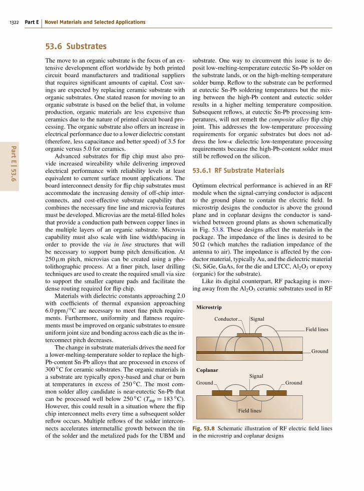
Optimum electrical performance is achieved in an RFmodule when the signal-carrying conductor is adjacentto the ground plane to contain the electric field. Inmicrostrip designs the conductor is above the groundplane and in coplanar designs the conductor is sand-wiched between ground plans as shown schematicallyin Fig. 53.8. These designs affect the materials in thepackage. The impedance of the lines is desired to be50� (which matches the radiation impedance of theantenna to air). The impedance is affected by the con-ductor material, typically Au, and the dielectric material(Si, SiGe, GaAs, for the die and LTCC, Al2O3 or epoxy(organic) for the substrate).
Like its digital counterpart, RF packaging is mov-ing away from the Al2O3 ceramic substrates used in RF
Microstrip
Ground
Conductor Signal
Field lines
Signal
Field lines
Ground Ground
Coplanar
Fig. 53.8 Schematic illustration of RF electric field linesin the microstrip and coplanar designs
Packaging Materials 53.7 Underfill and Encapsulants 1323Part
E|53.7
applications to the lower-cost solution of LTCC and or-ganic. The metalizations used are Cu on the interior ofthe substrates and Au as the top layer metalization toimprove RF performance.
Organic substrates offer a lower-cost solution. Thissubstrate is built in a laminate structure with punchedor laser drilled holes that are subsequently plated forinterlayer via interconnects. The laminant layers arevariations of epoxy and glass optimized for low di-electric constants. LTCC substrates are also laminantstructures of sheets of LTCC with laser drilled andplated vias. Recently, LTCC materials have been opti-mized to not shrink in the x-y plane during the sinteringprocess (z-direction shrinkage, however, is significant).The LTCC laminants are extremely thin compared toorganic, and offer the opportunity to build complex RFsubstrates.
An additional trend in RF substrate technology is tomove the discrete functions of RF module circuits fromsurface-mounted components to embedding them in thesubstrate. These embedded functions are typically ca-
pacitors and inductors and occasionally resistors. Thiscan be done because the substrate material is dielec-tric and metal; the basic components of passive devices.The advantages of embedding components are reducedsize, reduced cost and improved performance. Size canbe reduced because surface-mounted components takeup a great deal of the surface of the substrate. By em-bedding these components, they are thinner and area isreduced. Cost is reduced because the embedded pas-sives are formed as part of the laminant layers bypatterning the metal/dielectric and is essentially freebecause the patterning would be done regardless. Per-formance can be increased through the smaller sizeof the module. The embedding of components in sub-strates does offer opportunity for improved materials.Performance could be improved by finding means toalter the material properties of regions of the laminantlayers to optimize the electrical performance of discretecomponents that are to be embedded (i. e., seed regionsof the substrate for optimal capacitance, inductance andresistance).
53.7 Underfill and Encapsulants
53.7.1 Underfill
Flip chip technology demands that the space betweenthe chip and the substrate be filled with a dielectric or-ganic material to help mechanically interlock the chipto the substrate. The majority of underfill material avail-able is a silica-filled anhydride resin polymer. The fillerprovides the strength in the composite polymer andthe resin bonds with the die and substrate. Without theunderfill the difference in coefficient of thermal expan-sion between the chip (3 ppm=ıC) and the substrate(� 17 ppm=ıC) would quickly result in fracture of thesolder interconnects when variations in temperatureoccurred. New underfills must be developed to accom-modate increased bump density and shrinking bumpheight. As bump density increases and pitch decreases,the underfill must flow into smaller and smaller spaces.A 250�m pitch requires an underfill with a thickness of110�m. At a 150�m pitch, the dimension between thechip and substrate will be less than 50�m but 100% fillof underfill is still required. Traditional flow dispens-ing and cure may not be suitable in these thin spacesdue to a lack of capillary driving force (current un-derfill materials flow through a minimum thickness of75�m). For very thin fill spaces, wafer level depositionof the underfill needs to be developed. This wafer leveldeposition involves spin-on of an uncured polymer toa uniform thickness slightly less than the bump height.
The wafer would then be diced and die-mounted on sub-strates. Reflow would form the solder joints and curethe underfill simultaneously. The filled polymer mustbe spun to a uniform thickness of 25�m or less, bondwell with silicon and substrate materials, and be com-pliant.
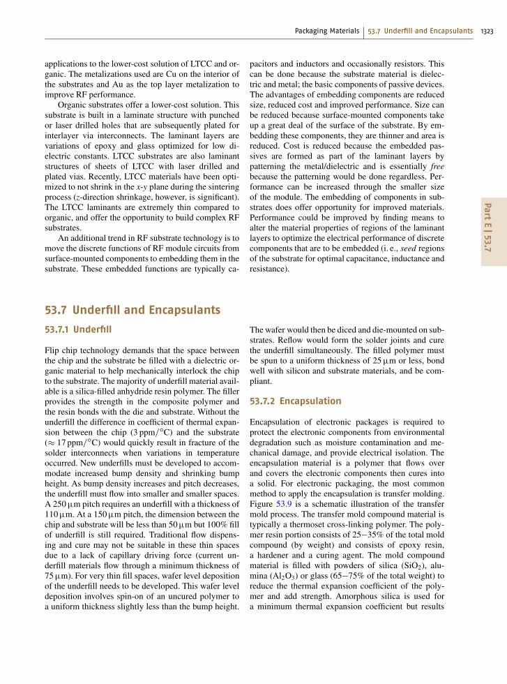
53.7.2 Encapsulation
Encapsulation of electronic packages is required toprotect the electronic components from environmentaldegradation such as moisture contamination and me-chanical damage, and provide electrical isolation. Theencapsulation material is a polymer that flows overand covers the electronic components then cures intoa solid. For electronic packaging, the most commonmethod to apply the encapsulation is transfer molding.Figure 53.9 is a schematic illustration of the transfermold process. The transfer mold compound material istypically a thermoset cross-linking polymer. The poly-mer resin portion consists of 25�35% of the total moldcompound (by weight) and consists of epoxy resin,a hardener and a curing agent. The mold compoundmaterial is filled with powders of silica (SiO2), alu-mina (Al2O3) or glass (65�75% of the total weight) toreduce the thermal expansion coefficient of the poly-mer and add strength. Amorphous silica is used fora minimum thermal expansion coefficient but results
PartE|53.8
1324 Part E Novel Materials and Selected Applications
Moldcompound
MoldCavity
Plunger
Heating element Gate
Pressure
Fig. 53.9 Schematic illustration of the transfer mold pro-cess
in a decrease in thermal conductivity. Crystalline sil-ica improves thermal conductivity but is abrasive to themolds. Small amounts of pigments (to color the moldcompound), accelerants, flame retardants, mold releaseagents, getterers, and antioxidants are also added to thefinal mold compound. Pellets of the mold compoundare placed into a heated cavity at the top of the moldand pressure is applied by a ram that pushes the lique-fying materials into the mold. The material is forcedthrough channels and through a constriction (calledthe gate) that provides back pressure and regulates theflow rate of the molten mold compound. After passingthrough the gate, the mold material flows across thecomponent being encapsulated. The heat is turned offand upon cooling the polymer cross-links, with the useof a curing agent (typically an amine) that is presentin the mold compound. The mold compound materialhas good adhesion, good stability with regards to tem-perature, chemicals, and the environment. They curerapidly, have low permeability to moisture and high di-electric strength.
The transfer mold process has the advantage thatpart dimensions are very well controlled. The processand materials are low cost and high-volume manufac-turing is possible.
An issue with mold compound encapsulation pro-cessing is wire sweep where the force of the viscous
encapsulant can push bond wires to short with one an-other. This has been addressed with optimized filler sizeand shape and the mold temperature and pressure. Aftermolding, the difference in thermal expansion betweenthe cured mold compound and the rest of the package(the substrate, leadframe, semiconductor device, etc.)can result in considerable stresses at the interfaces. Fur-thermore, the CTE of mold compounds changes whenthe material goes above the glass transition temperature,Tg. Tg is the temperature at which the polymer changesfrom a rigid structure to a softer more glass-like struc-ture. Below Tg, the CTE of typical mold compoundsis 20�10�6 .ıC/�1 but above Tg this can increase to60�10�6 .ıC/�1 or 70�10�6 .ıC/�1. The Tg of moldcompounds varies but is usually 175�200 ıC, below thesolder processing temperatures that are typically in ex-cess of 220 ıC. After cooling from mold processing,the mold compound forms a compression seal with thelower expanding materials (leadframe, substrate, semi-conductor). However, upon heating to solder processtemperatures the stress is reversed to tensile and canresult in interfacial cracking, or delamination. The in-terfacial cracks provide a conduit for the ingress ofwater or ionic contaminants that could result in cor-rosion of metals in the package (particularly Al bondpads). This issue must be addressed by optimizing themold compound to the package application (materialsand size) to minimize strain and to maximize interlock-ing mechanisms between the mold compound and thesubstrate/leadframe.
Mold compound encapsulation is generally detri-mental to RF device performance. The encapsulantmaterials are nonuniform and degrade performance be-cause the electric field generated by the RF circuit inthe encapsulant is nonuniform resulting in lossy behav-ior. Many high-performance RF packages are designedwith a cavity and are made out of ceramic with a metallid to form the cavity. However, plastic encapsulationis required for suitable, low-cost, reliable packages, soa trade-off must be made for performance, reliabilityand cost.
53.8 Electrically Conductive Adhesives (ECAs)
Electrically conductive adhesives (ECAs) are compos-ite materials consisting of a dielectric curable poly-mer and metallic conductive particles. ECAs are low-process temperature alternatives to solder alloys. Thepolymer is an adhesive material that chemically reactswith metals to form a bond. The metallic particles in theadhesive form a network in the cured joint that formsa conduction path in area-array applications.
53.8.1 Adhesive Polymers
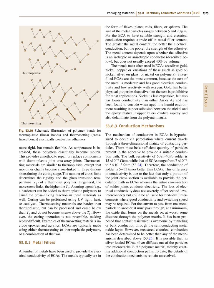
The polymer portion of the adhesive is available in twoforms: thermoplastic and thermosetting. A schematicillustration of these two types of polymers is shownin Fig. 53.10. A thermoplastic polymer is a linearchain of linkedmonomers (nominally, hydrogen-carbonbonds). After curing, thermoplastic polymers become
Packaging Materials 53.8 Electrically Conductive Adhesives (ECAs) 1325Part
E|53.8
Thermoplastic
Thermosetting
Fig. 53.10 Schematic illustration of polymer bonds forthermoplastic (linear bonds) and thermosetting (cross-linked bonds) electrically conductive adhesives
more rigid, but remain flexible. As temperature is in-creased, these polymers essentially become molten.This provides a method to repair or replace componentswith thermoplastic joint area-array joints. Thermoset-ting materials are similar to thermoplastic, except thatmonomer chains become cross-linked in three dimen-sions during the curing stage. The number of cross-linksdetermines the rigidity and the glass transition tem-perature (Tg) of a thermoset polymer. In general, themore cross-links, the higher the Tg. A curing agent (e.g.,a hardener) can be added to thermoplastic polymers tocause the cross-linking reaction in these materials aswell. Curing can be performed using UV light, heat,or catalysts. Thermosetting materials are harder thanthermoplastic, but can be processed and cured belowtheir Tg and do not become molten above the Tg. How-ever, the curing operation is not reversible, makingrepair difficult. Examples of thermosetting materials in-clude epoxies and acrylics. ECAs are typically madeusing either thermosetting or thermoplastic polymers,or a combination of the two.
53.8.2 Metal Fillers
A number of metals have been used to provide the elec-trical conductivity of ECAs. The metals typically are in
the form of flakes, plates, rods, fibers, or spheres. Thesize of the metal particles ranges between 5 and 20�m.For the ECA to have suitable strength and electricalconduction requires a trade-off in metal filler content.The greater the metal content, the better the electricalconduction, but the poorer the strength of the adhesive.The metal content depends upon whether the adhesiveis an isotropic or anisotropic conductor (described be-low), but does not usually exceed 40% by volume.
The metals most often used in ECAs are silver, gold,nickel, copper or variations of these (such as gold onnickel, silver on glass, or nickel on polymers). Silver-filled ECAs are the most common, because the cost ofthe metal is moderate and has good electrical conduc-tivity and low reactivity with oxygen. Gold has betterphysical properties than silver but the cost is prohibitivefor most applications. Nickel is less expensive, but alsohas lower conductivity than either Au or Ag and hasbeen found to corrode when aged in a humid environ-ment resulting in poor adhesion between the nickel andthe epoxy matrix. Copper fillers oxidize rapidly andalso delaminate from the polymer matrix.
53.8.3 Conduction Mechanisms
The mechanism of conduction in ECAs is hypothe-sized to occur via percolation where current travelsthrough a three-dimensional matrix of contacting par-ticles. There must be a sufficient quantity of particlespresent in the adhesive to provide a suitable conduc-tion path. The bulk resistivity of 60Sn-40Pb solder is15�10�6�cm, while that of ECAs range from 7�10�5
to 5�10�4�cm [53.24]. Therefore, the conduction ofsolder is 5�33 times better than ECAs. This differencein conductivity is due to the fact that only a portion ofthe joint cross-section is available to provide the per-colation path in ECAs whereas the entire cross-sectionof solder joints conducts electricity. The loss of elec-trical conductivity does not severely affect second-levelinterconnects but could be an issue for first-level inter-connects where good conductivity and switching speedmay be required. For the current to pass from one metalparticle to another, it must pass through, at a minimum,the oxide that forms on the metals or, at worst, somedistance through the polymer matrix. It has been pro-posed that contact resistance is overcome by tunnelingor bulk conduction through the semiconducting metaloxide layer. However, measured electrical conductionhas been determined to be better than any of the mech-anisms described above [53.25]. It is possible that, insilver-loaded ECAs, silver diffuses out of the particlesinto microcracks in the polymer matrix, thereby creat-ing additional conduction paths. To date, the details ofthe conduction mechanisms remain unresolved.
PartE|53.9
1326 Part E Novel Materials and Selected Applications
Metalparticles
Polymermatrix
ConductionpathPadBoard
Package lead
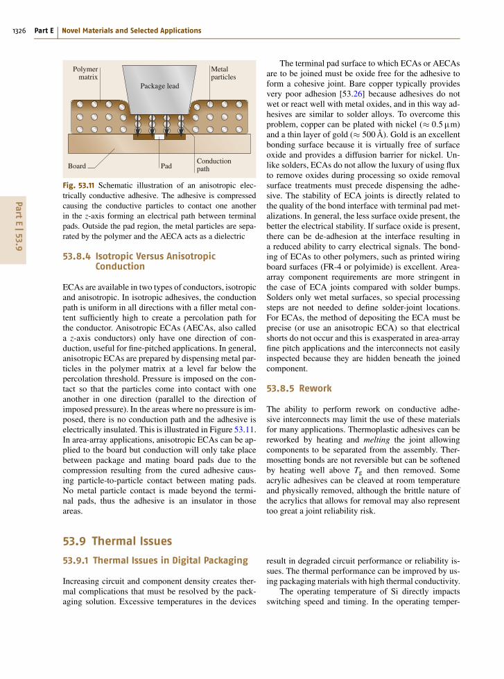
Fig. 53.11 Schematic illustration of an anisotropic elec-trically conductive adhesive. The adhesive is compressedcausing the conductive particles to contact one anotherin the z-axis forming an electrical path between terminalpads. Outside the pad region, the metal particles are sepa-rated by the polymer and the AECA acts as a dielectric
53.8.4 Isotropic Versus AnisotropicConduction
ECAs are available in two types of conductors, isotropicand anisotropic. In isotropic adhesives, the conductionpath is uniform in all directions with a filler metal con-tent sufficiently high to create a percolation path forthe conductor. Anisotropic ECAs (AECAs, also calleda z-axis conductors) only have one direction of con-duction, useful for fine-pitched applications. In general,anisotropic ECAs are prepared by dispensingmetal par-ticles in the polymer matrix at a level far below thepercolation threshold. Pressure is imposed on the con-tact so that the particles come into contact with oneanother in one direction (parallel to the direction ofimposed pressure). In the areas where no pressure is im-posed, there is no conduction path and the adhesive iselectrically insulated. This is illustrated in Figure 53.11.In area-array applications, anisotropic ECAs can be ap-plied to the board but conduction will only take placebetween package and mating board pads due to thecompression resulting from the cured adhesive caus-ing particle-to-particle contact between mating pads.No metal particle contact is made beyond the termi-nal pads, thus the adhesive is an insulator in thoseareas.
The terminal pad surface to which ECAs or AECAsare to be joined must be oxide free for the adhesive toform a cohesive joint. Bare copper typically providesvery poor adhesion [53.26] because adhesives do notwet or react well with metal oxides, and in this way ad-hesives are similar to solder alloys. To overcome thisproblem, copper can be plated with nickel (� 0:5�m)and a thin layer of gold (� 500Å). Gold is an excellentbonding surface because it is virtually free of surfaceoxide and provides a diffusion barrier for nickel. Un-like solders, ECAs do not allow the luxury of using fluxto remove oxides during processing so oxide removalsurface treatments must precede dispensing the adhe-sive. The stability of ECA joints is directly related tothe quality of the bond interface with terminal pad met-alizations. In general, the less surface oxide present, thebetter the electrical stability. If surface oxide is present,there can be de-adhesion at the interface resulting ina reduced ability to carry electrical signals. The bond-ing of ECAs to other polymers, such as printed wiringboard surfaces (FR-4 or polyimide) is excellent. Area-array component requirements are more stringent inthe case of ECA joints compared with solder bumps.Solders only wet metal surfaces, so special processingsteps are not needed to define solder-joint locations.For ECAs, the method of depositing the ECA must beprecise (or use an anisotropic ECA) so that electricalshorts do not occur and this is exasperated in area-arrayfine pitch applications and the interconnects not easilyinspected because they are hidden beneath the joinedcomponent.
53.8.5 Rework
The ability to perform rework on conductive adhe-sive interconnects may limit the use of these materialsfor many applications. Thermoplastic adhesives can bereworked by heating and melting the joint allowingcomponents to be separated from the assembly. Ther-mosetting bonds are not reversible but can be softenedby heating well above Tg and then removed. Someacrylic adhesives can be cleaved at room temperatureand physically removed, although the brittle nature ofthe acrylics that allows for removal may also representtoo great a joint reliability risk.
53.9 Thermal Issues
53.9.1 Thermal Issues in Digital Packaging
Increasing circuit and component density creates ther-mal complications that must be resolved by the pack-aging solution. Excessive temperatures in the devices
result in degraded circuit performance or reliability is-sues. The thermal performance can be improved by us-ing packaging materials with high thermal conductivity.
The operating temperature of Si directly impactsswitching speed and timing. In the operating temper-
Packaging Materials References 1327Part
E|53
ature range of 50�100 ıC, a 5 ıC drop in operatingtemperature results in a 1% increase in CMOS switch-ing speed. From a reliability perspective, each 10 ıCincrease in operating temperature results in a 2� in-crease in the die failure rate. Therefore, packagingmaterials and processes that improve thermal perfor-mance are very important.
New materials are the area where the most signif-icant improvements in thermal performance are pos-sible. Improved thermal interface materials (greases,adhesives, tapes, phase change materials) will improvethe heat flow out of the package. Improved adhesivesand compliant sheets inside the package will improveheat dissipation from the die and can better accommo-date CTE mismatch strains within the package.
Composite materials for package lids, heat spread-ers and heat sinks are needed. Currently, these compo-nents face a dilemma of conflicting material propertiesof good thermal conduction materials (e.g., Al) havevery high CTE (e.g., Al D 25�10�6 =ıC) that can re-sult in poor reliability. Furthermore, most low-costthermal conductors are also electrical conductors mak-ing their use in dielectric packages problematic. Thedevelopment of composite materials with anisotropicconductivities can provide excellent thermal conductionwith matched CTE and the potential for a good elec-trical isolation. At the die level, the use of low-costthin-film diamond must increase. Diamond has excel-lent thermal conductivity and isolation but is currentlytoo expensive for extensive use in microelectronic pack-aging.
53.9.2 Thermal Issues in RF Packaging
RF die can generate a great deal of heat in operat-ing at high frequencies. This is particularly an issuewith GaAs die because it has poor thermal conductiv-ity (30W/mK). The generated heat must be dissipatedthrough the package. The preferred method to removeheat from wirebonded GaAs die is to thin the GaAswafer by back-grinding to 100�125�m. The thinnerthe die, the easier it is to transmit heat through theGaAs. Through-die vias are also used to help dissi-pate heat. The vias are formed by laser drilling holesthrough the GaAs then plating the side walls with Auand thinning the wafer. Thinning the wafer not onlybenefits heat dissipation but also reduces the distancefrom the conducting layer on the surface of the dieto the ground plane on the die backside that improvesimpedance match in microstrip designs.
The problems with through-die vias and wafer thin-ning are cost and die breakage. Laser drilling and thin-ning processes increase the cost of the die. Furthermore,GaAs is a very brittle material, so that the presence ofvias and thinning exacerbates potential cracking.
One method to reduce the thermal and mechanicalproblems associated with thermal issues on GaAs is touse flip chip interconnects. For flip chip, the bumps actas electrical, mechanical and thermal interconnects. Thebumps are on the front side of the die so full thicknessdie can be used. The challenge with flip chip as a ther-mal conductor is to put sufficient numbers of bumps onthe die to dissipate the heat.
53.10 SummaryMaterials are one of the most important aspects ofmicroelectronic packaging. There is a need for newmaterials to be developed to meet the ever-changing re-quirements for high-speed digital and RF applications.Considerable resources are required to develop andcharacterize these materials. These materials must alsobe tested to determine their compatibility with assembly
processes and device performance and meet industrystandards. The fundamental material characteristics thatmust be understood, depending upon the material, in-clude: dielectric constant, dielectric loss, conductivity,resistivity, moisture absorption, glass transition tem-perature, strength, time dependent deformation (creep),and fracture toughness.
References
53.1 D.R. Frear, W.B. Jones, K.R. Kinsman: Solder Me-chanics: A State of the Art Assessment (TMS, War-rendale 1991)
53.2 K. Puttlitz, P. Totta (Eds.): Area Array Packaging(Kluwer, Dordrecht 2001)
53.3 P.A. McCluskey (Ed.): High Temperature Electronics(CRC, Boca Raton 1996)
53.4 J.H. Lau: Ball Grid Array Technology (McGraw–Hill,New York 1995)
53.5 G. Harmann: Wire Bonding in Microelectronics Ma-terials, Processes, Reliability, and Yield (McGraw–Hill, New York 1997)
53.6 R.J. Klein Wassink: Soldering in Electronics (Elec-trochem. Publ., Ayr, Scottland 1989)
PartE|53
1328 Part E Novel Materials and Selected Applications
53.7 C.A. Harper: Electronic Packaging and Interconnec-tion Handbook (McGraw–Hill, New York 1991)
53.8 M.L. Minges (Ed.): Electronic Materials Handbook:Packaging, Vol. 1 (ASM-Int., Materials Park 1989)
53.9 H. Clauberg, I. Qin, P. Reid, B. Chylak: Fine pitchcopper wire bonding, Chip Scale Rev. 14(6) (2010)
53.10 P. Chauhan, A. Choubey, Z.W. Zhong, M. Pecht: Cop-per Wire Bonding (Springer, New York 2014)
53.11 E. Philofsky: Intermetallic formation in Au-Al sys-tems, Solid State Electron. 13, 1391 (1970)
53.12 C. Horsting: Purple Plague and Au Purity, Proceed-ings 10th Annual IRPS (IEEE, Westmoreland 1972)p. 155
53.13 L. Levine, M. Sheaffer: Wirebonding strategies tomeet thin film packaging requirements – Part 1,Solid State Technol. 36, 63 (1993)
53.14 L.S. Goldman: Geometric optimization of controlledcollapse interconnects, IBM J. Res. Dev. 13, 251(1969)
53.15 J.-K. Lin, J. Drye, W. Lytle, T. Scharr, R. Sharma: Con-ductive Polymer Bump Interconnects, Proceedingsof the 46th Electronic Components Technology Con-ference (IEEE, Piscataway 1996) p. 1059
53.16 N.C. Lee: Pb-free soldering – Where the worldis going, Adv. Microelectron (IEEE, Piscataway, NJ1999) p. 29
53.17 J. Glazer: Microstructure and mechanical propertiesof Pb-free solder alloys for low-cost electronic as-sembly: A review, J. Electron. Mater. 23, 693 (1994)
53.18 J. Glazer: Metallurgy of low temperature Pb-freesolder for electronic assembly, Int. Mater. Rev. 40,65 (1995)
53.19 M. Abtew, G. Selvardery: Pb-free solder in micro-electronics, Mater. Sci. Eng. 27, 95 (2000)
53.20 H.K. Seelig, D. Suraski: The status of Pb-free solderalloys, Proc. 50th Electron. Comp. Tech. Conf. (IEEE,Piscataway 2000) p. 1405
53.21 K.G. Snowden, C.G. Tanner, J.R. Thompson: Pb-freesoldering interconnects: Current status and futuredevelopments, Proc. 50th Electron. Comp. Tech.Conf. (IEEE, Piscataway 2000) p. 1416
53.22 Z. Hasnain, A. Ditali: Building-in reliability: Softerrors – a case study, Ann. Proc. Reliab. Phys (IEEE,Westmoreland 1992) p. 276
53.23 M.W. Roberson, P.A. Deane, S. Bonafede, A. Huff-man, S. Nangalia: Conversion between standardand low-alpha Pb in solder bumping productionlines, J. Electron. Mater. 29, 1274 (2000)
53.24 H.L. Hvims: Conductive adhesives for SMT and po-tential applications, IEEE Trans. Components Hy-brids Manuf. Technol. 18, 284 (1995)
53.25 L.C. Li, H. Lizzul, I. Kim, J.E. Sacolick, J.E. Morris:Electrical, structural and processing properties ofelectronic conductive adhesives, IEEE Trans. Com-ponents Hybrids Manuf. Technol. 16, 843 (1993)
53.26 D.D.L. Chang, J.A. Fulton, H.C. Ling, M.B. Schmidt,R.E. Sinitiski, C.P. Wong: Accelerated life test of z-axis conductive adhesives, IEEE Trans. ComponentHybrids Manuf. Technol. 16, 836 (1993)